
 Open Access Article
 This Open Access Article is licensed under a
 Creative Commons Attribution 3.0 Unported Licence
Defect engineering in antimony selenide thin film solar cells
Udari
Wijesinghe
,
Giulia
Longo
and
Oliver S.
Hutter
 *
*
Department of Mathematics, Physics, and Electrical Engineering, Northumbria University, Newcastle upon Tyne NE1 8QH, UK. E-mail: oliver.hutter@northumbria.ac.uk
First published on 21st October 2022
Abstract
Antimony selenide (Sb2Se3) has gained promising attention as an inorganic absorber in thin-film photovoltaics and water splitting devices due to its excellent optoelectronic properties, low toxicity, and earth abundancy. Presently, Sb2Se3 solar cells have a record power conversion efficiency of 10.12%, with a rapid rise over the past few years. However, further efficiency increases are hindered by the severe open circuit voltage deficit associated with the defects and interfacial recombination. The existing defects impact charge carrier generation, transportation, intrinsic electrical conductivity, and film crystallinity which inevitably influences the efficiency and stability of polycrystalline Sb2Se3 solar cells. Thus, effective defect engineering aiming at understanding the chemical nature of defects is essential to enhance the inferior performance and functional properties of Sb2Se3 thin films. Herein, a comprehensive review of the defect chemistry at surfaces, grain boundaries, and interfaces in Sb2Se3 solar cells, and efforts made in the community to passivate these defect states are presented. Finally, the potential challenges associated with an in-depth understanding of defect dynamics and strategies to achieve highly efficient and stable Sb2Se3 solar cells in the future are provided.
1. Introduction
A globally increasing energy demand has resulted in a growing search for sustainable, reliable, and affordable photovoltaic (PV) materials. Currently, polycrystalline silicon (Si), cadmium telluride (CdTe), and copper indium gallium selenide (Cu(In,Ga)Se2, CIGS) are used as dominant absorbers in solar cells and have all achieved a certified power conversion efficiency (PCE) of over 20%.1–3 However, the high processing cost of Si, the toxicity of Cd, the high price of Ga and In, and the scarcity of In, Ga, and Te is a challenging task for the mass production of thin-film solar cells from these materials.3,4 Kesterite solar cells (Cu2ZnSn(SxSe1−x)4, CZTS/Se) reached peak device efficiencies of around 12.7% in 2021.5 But the rise in efficiency stagnated for years due to defects associated with the complex phase chemistry of the material. Recently, the development of halide perovskites (CH3NH3PbI3) has progressed rapidly with impressive peak device efficiencies of around 25% for perovskite materials.2 However, the instability and the toxicity of lead (Pb) based perovskites drive sustained research on novel absorbers for thin-film PVs.4,6Over the last decade, antimony selenide (Sb2Se3) has gained tremendous attention in the PV regime due to a high optical absorption coefficient (105 cm−1) across the visible range, a suitable bandgap of 1.1–1.3 eV, high carrier mobility (10 cm2 V−1 s−1), low toxicity, simple phase chemistry, low cost, and high elemental abundance.7–11 It has also yielded promising results in photoelectrochemical water splitting devices.12–15 Unlike conventional absorbers, Sb2Se3 displays a unique quasi-one-dimensional (Q1D) structure composed of [Sb4Se6]n ribbons, where ribbons are held together by van der Waals forces without dangling bonds, while the Sb–Se atoms within the ribbons are covalently bonded.8,9,16 However, a recent study based on first-principles calculations showed that inter-ribbon interactions in Sb2Se3 fall between the van der Waals and covalent regime.17 Other works revealed that tailoring the growth orientation of [Sb4Se6]n chains closer to perpendicular to the substrate in the [211] and [221] crystal planes reduce the density of dangling bonds and create intrinsically benign grain boundaries (GBs).9,18–20 Nevertheless, ribbons in the [001] plane significantly minimize non-radiative recombination losses improving the utility of Sb2Se3 polycrystalline thin films in PVs.21,22 For most known inorganic absorbers (such as Si, CIGS, and CdTe), the breakage of covalent bonds inevitably introduces defect states and recombination centers at the GBs, which can effectively block charge collection and potentially reduce device efficiency during the interface recombination. Contrastingly, Sb2Se3 has intrinsically benign GBs which could therefore offer a sustainable solution to drawbacks associated with traditional absorber materials if efficiency values continue to rise.
Sb2Se3 is still relatively under studied compared to other technologies such as kesterite and perovskite materials. To illustrate this, Fig. 1(a) provides a statistical analysis of publications related to Sb2Se3 solar cells between 2015 and 2022. Three main areas of research within the field currently are control of the orientation of Sb2Se3 films,9,18–20 band alignment optimization,23–29 and defect passivation at interfaces/surfaces to suppress recombination losses and the open circuit voltage (VOC) deficit.30–36 Despite the excellent properties of Sb2Se3, PCEs values are still far below the maximum theoretical value of 30% predicted by the Shockley–Queisser (S–Q) model (Fig. 1(b)).37 Spectroscopic limited maximum efficiency (SLME) calculations show that Sb2Se3 has great room for development of highly efficient solar cells with an upper limit of 30%, which is actually higher than both CdTe and CZTS/Se.38 Different physical and chemical techniques have been employed to fabricate Sb2Se3 solar cells with high crystallinity that are essential to enhance conductivity, carrier separation and stability,7,9,18,21,35,39–49 and PCEs have rapidly risen from 0.66% in 2009 to over 9.2% in 2019,10,18,21,35,39,50–52 with highest recorded efficiency of 10.12% in 2022.53
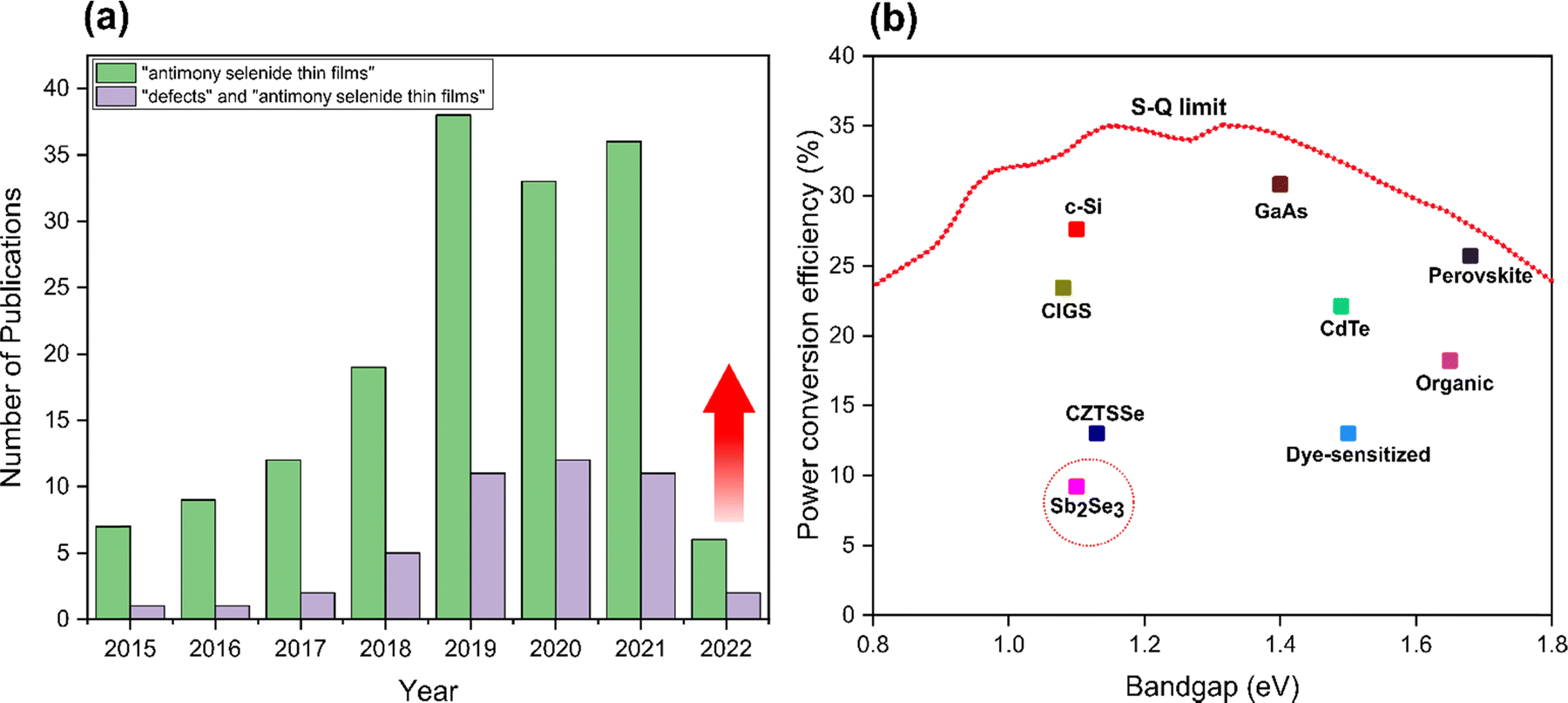 | ||
| Fig. 1 (a) The number of publications regarding Sb2Se3 thin-film solar cells and defects analysis of Sb2Se3 thin-film solar cells from 2015 to 2022 (data extracted from Web of Science). (b) Peak reported single junction efficiencies for different absorber materials in comparison to the S–Q limit. | ||
Peak Sb2Se3 PCEs are critically confined by a large VOC deficit (Eg/q − VOC, where Eg is the optical bandgap of the Sb2Se3, and q is the elementary charge), which is far beyond the estimated losses according to the S–Q limit (0.24–0.28 V) for a band gap range from 1.0 to 1.7 eV.54,55 Moreover, there is a conspicuous gap in studies on the origins of VOC losses and defect analysis of thin films (Fig. 1(a)). This is due to the defect chemistry of Sb2Se3 being complex, and fundamental features such as carrier mobility, carrier lifetime, diffusion length, defect depth, defect density, and band tailing being mostly unexplored. Compared to Sb2Se3, the higher band gap sulfide analogue (Sb2S3) and it's alloys Sb2(S,Se)3 also exhibit similar advantages, and the disadvantage of a large VOC deficit for champion devices.56,57 Reported efficiencies of Sb2S3 and Sb2(S,Se)3 solar cells are still relatively low, encountering the problem of high resistivity of the absorber, low charge extraction from the absorbing layer to the buffer layer, and easy formation of point defects deep inside the bandgap that act as electron–hole non-radiative recombination centers.58,59 Thorough understanding is lacking because of three difficulties: (i) low electrical conductivity (10−6–10−7 S cm−1) in Sb2Se3 film leads to difficulty in analyzing carrier density and mobility directly from the Hall effect,7,10,40,60 (ii) extremely limited band-to-band recombination which makes challenging the study of carrier lifetime and defect information from photoluminescence (PL),40,61 (iii) strong anisotropy which renders mobility measurements very complicated.21,40,55,62 In addition, defect analysis has been assessed based on the determining carrier type in the absorber, although the results are typically from a single group and often inconclusive. In most studies, it is assumed that the Sb2Se3 absorber is predominantly p-type without determining the minority carrier type.63–66 On the basis of Hall effect measurements, cyclic voltammetry, deep-level transient spectroscopy (DLTS), and X-ray photoelectron spectroscopy (XPS) analysis reported that Sb2Se3 films show p-type character.10,31,39,67 Whereas Hobson et al. revealed unintentional introduction of chlorine (Cl) impurities present in the purchased source material formed n-type Sb2Se3 absorber.36 Furthermore, due to the presence of extrinsic dopants such as iodine (I)44,68 and tellurium (Te),32,69–71 the possibility of formation of n-type devices with high efficiencies also exists. Hence, it's vitally important to consider the source of the Sb2Se3 material and any impurities that may be present in the growth or processing environment, as Sb2Se3 in solar cells can behave as both p-type or n-type absorbers. However, the n-type character remains less explored in the area of thin film Sb2Se3 PVs and many other groups may well be fabricating highly efficient devices where the Sb2Se3 can be unknowingly n-type. Therefore, the actual carrier type of Sb2Se3 is not ambiguously clear, and the assumption of Sb2Se3 as a p-type material without experimental validation might result in erroneous defect physics.
Defects are unavoidable in thin film fabrication, and these affect the charge carriers transport, lifetime, recombination rate, the carrier concentrations tuning, doping limit, and Fermi level for realizing the functionality of the material (i.e., p-type and n-type). The defects can form intrinsically (i.e., vacancies: by the presence of missing atoms; self-interstitials: added atoms in between expected atoms position; antisites: exchanged atoms in the crystal structure) or extrinsically (i.e., by the presence of foreign atoms in the crystal structure). The dislocation of atoms from the native lattice creates electronic states inside the band gap. In general, defects with low formation energies imply easy formation. The defects formed within a few kBT (∼0.025 eV at 300 K, where kB is Boltzmann constant and T is temperature) from the conduction band minimum (CBM) usually act as shallow donors, whereas defects closer to valence band maximum (VBM) generally act as shallow acceptors. If the defect state is sufficiently shallow, it will readily ionize, transferring the electrons/holes to the CBM/VBM or to defect levels closer to CBM/VBM at room temperature. For easy reference, the energy levels of Sb2Se3 are summarized in Fig. 2(a). In contrast, defects that introduce levels deep in the bandgap with energy much higher than kBT form deep level defects (Fig. 2(b))32,39,72,73 The trap states associated with deep defects usually act as detrimental traps for photogenerated carriers and act as recombination centers and dictate carrier mobility, which ultimately affects the efficiency of the device; thus, the formation of these should be avoided. Fig. 2(b) shows a simplified version of these defect levels, which does not take into account the possibility of defects changing energy through lattice relaxation upon charge capture.74
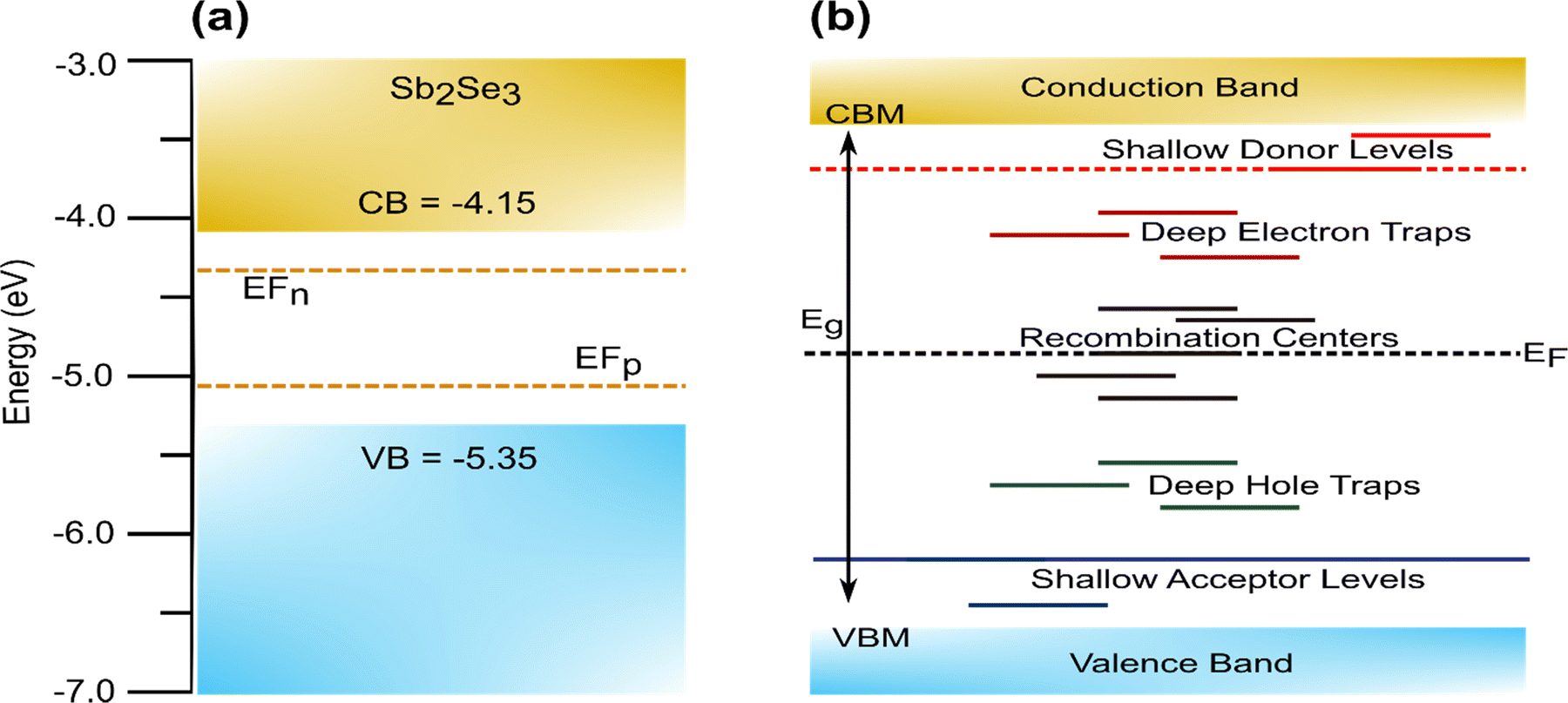 | ||
| Fig. 2 (a) Schematic band structure of Sb2Se3 with electron and hole quasi Fermi level (EFn and EFp). (b) Simplified schematic band diagram with different defect states in a typical semiconductor material. | ||
In order to characterize and provide useful information on the trap states and defects in Sb2Se3, computational studies such as first-principles calculations,30 hybrid density functional theory (DFT),75–78 and various experimental detection techniques are used. Time-resolved transient absorption (TRTA) spectroscopy is used to identify the dynamics of photogenerated carriers and defect density states of the absorber.7,79,80 Temperature-dependent dark conductivity and thermal admittance spectroscopy (TAS) can determine the depth and density of defect states.7,40 DLTS,36,39 capacitance–voltage (C–V),19 and capacitance–frequency (C–F)7,80 are used to measure dopant concentration distribution in the absorber and to differentially identify interfacial defects from bulk defects. Furthermore, recombination mechanisms and related defects in an absorber are directly characterized through PL spectroscopy.43,81 Lastly, deep level capacitance profiling (DLCP) is used to analyze minority-carrier traps in the absorber by measuring capacitance changes with voltage pulses as a function of temperature.19,40
Herein, this article provides an essential insight into defects associated with absorber surface, GBs, and interfaces and their impact on Sb2Se3 device performance. Moreover, recent achievements and techniques used to suppress the defect states and VOC issues, including passivation of point defects, post-treatments, surface modifications, and interfacial modifications, are presented. Finally, we provide current challenges and future research directions for defect control of Sb2Se3 solar cells for further improvement of PV performance.
2. Defect chemistry of antimony selenide thin films
Defect tolerance (i.e. when no deep level defects are formed in the bandgap) is a highly desirable characteristic of a PV absorber.82,83 Unintentional defects present in thin film absorbers often degrade the physicochemical and photoelectrical properties of PV devices.3,30,75 Having simple binary phase chemistry, Sb2Se3 was initially expected to have simple intrinsic point defects with benign defect properties, and defect control should have therefore been much easier than that in quaternary compounds such as CZTS/Se.6,78 As such, it was expected to have six possible point defects. These are (i) two vacancies (cation vacancy, VSb, and anion vacancy, VSe). (ii) Two interstitials (cation interstitial, Sbi, and anion interstitial, Sei). (iii) Two substitutions (cation-replace-anion antisite, SbSe, and anion-replace-cation antisite, SeSb).30,78,84 However, the experimental and theoretical results have demonstrated that intrinsic defects in Sb2Se3 are unexpectedly complicated and unconventional, and the defect physics in this Q1D van der Waals system cannot be simply adopted from those in the three-dimensional covalent binary PV absorbers such as GaAs and CdTe (where all the cation/anion sites remain identical).3,30,55,75 This is mainly for two reasons. Firstly, due to the low symmetry of the Q1D structure, identical defects located on non-equivalent atomic sites can exhibit very different defect properties, i.e., a single Sb2Se3 ribbon shows three nonequivalent Se atomic sites (Se1, Se2, and Se3) and two Sb atomic sites (Sb1 and Sb2 in Fig. 3). Therefore, defects associated with different atomic sites can be very different. Secondly, due to the weak van der Waals interactions between [Sb4Se6]n ribbons, large voids present between different [Sb4Se6]n atomic chains create uncommon defects which are difficult to form in convectional absorbers, e.g., cation-replace-anion antisite (SbSe), anion-replace-cation antisite (SeSb), and even two-anion-replace-one-cation antisite (2SeSb). Therefore, although there are only a few types of point defects, the properties of these point defects are complicated by structural freedom.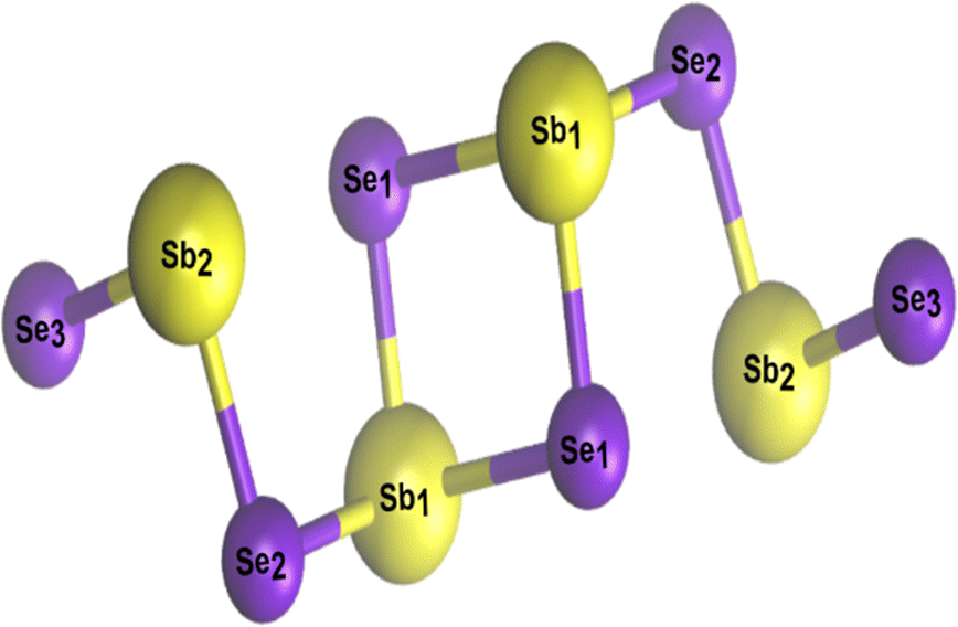 | ||
| Fig. 3 Non-equivalent atomic sites in [Sb4Se6]n atomic chain. | ||
As previously mentioned, crystalline defects can be broadly divided into two main categories called intrinsic and extrinsic defects. Furthermore, based on their dimensions, defects are categorized as point defects (0D), linear defects (1D), interfacial/planar defects (2D), and bulk/volume defects (3D).3,73,85 All these types of defects can coexist and interact in various ways and one of these defects can then dominate to change the properties of Sb2Se3 films, whereas others could be trivial.30,85 The fabrication approach is mainly responsible for the density and the type of defects regardless of different device configurations (n–p or n–i–p or n–n). The following section discusses the experimental and theoretical findings of intrinsic and extrinsic defects in Sb2Se3 thin films and their intrinsic behavior towards solar cells' conductivity and VOC deficit.
Before entering into the details of defect formation and behavior in Sb2Se3, it is important to briefly explain some fundamental concepts that will be largely used in this review. Firstly, it is worth stressing the difference in meaning between “formation energy”, “transition/activation energy” and “ionization energy” of defects. Formation energy describes the Gibbs free energy necessary for the formation of defects. The lower it is, the easier it is for defects to form, and consequently they will exist in higher concentration. The “transition/activation energy” refers to the position of the traps with respect to the conduction and valence bands (ECBM − ET for electron traps and ET − EVBM for hole traps, where ET is the energy level of defect, ECBM is the energy of CBM, and EVBM is the energy of VBM). The lower the activation energy, the easier it is to de-trap trapped charges. Finally, the “ionization energy” is the energy required for the trap to reduce or oxidize.
Defects can be neutral or ionized. The doping and trapping effect of charged defects is depicted in Fig. 4. If an anion with energy levels close to the CBM is introduced in the material it will likely enhance the electron concentration, acting as an n-dopant and increasing the Fermi level of the material. If the energy levels introduced by this anion are located in the middle of the bandgap or, even worse, close to the VBM, it would then annihilate holes, acting as an electron trap. The opposite would happen for cations with p-doping/electron trapping effect. However, the effect of neutral defects, especially intrinsic, can be more challenging to understand, and need careful characterization. A vacancy of selenium VSe, for example, corresponds to a missing Se0 atom. This means that the electrons shared between the Sb–Se, which would naturally be localized around the more electronegative Se, are now less bounded and available to be promoted in the conduction band. For this to happen, the neutral vacancy is ionized:
| V0Se → V+Se + e− |
| V+Se → V2+Se + e− |
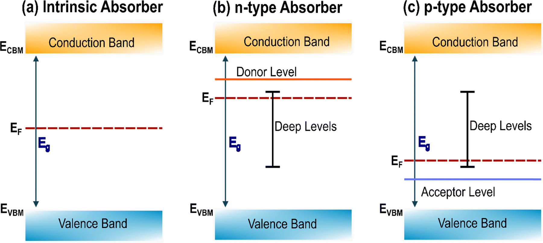 | ||
| Fig. 4 Schematic illustration of Fermi level position (EF), donor, and acceptor ionization energy levels within the band gap (Eg) of different type of absorbers (a) intrinsic absorber, (b) n-type absorber, and (c) p-type absorber. | ||
A VSe defect then acts as a donor, provided that the ionization energy of ∼0.53 eV for this process to happen in equilibrium conditions.76,86
2.1. Intrinsic defects
The high VOC deficit of devices fabricated using intrinsic Sb2Se3 is known to be one critical limitation to the performance of Sb2Se3-based solar cells. Currently, the best performing Sb2Se3 solar cells have a deep defect density of 1014–1015 cm−3, which is much higher than those in CdTe solar cells (1011–1013 cm−3).18,39,87 Moreover, the free carrier concentration of undoped Sb2Se3 being limited to ∼1013 cm−3 confirms that a high concentration of defects exists in the un-ionized form.7,87 To understand the correlation between defect-assisted recombination and VOC loss, intrinsic point defects have been studied by first-principles calculation and DFT studies.30,75,77,78 The defect formation energies of all the non-equivalent sites of VSe (Se vacancy), VSb (Sb vacancy), Sei (Se interstitial), Sbi (Sb interstitial), SeSb (Se replace Sb antisite), and SbSe (Sb replace Se antisite) were calculated under the Se-rich and Se-poor conditions (Fig. 5(a) and (b)).30,75,78,84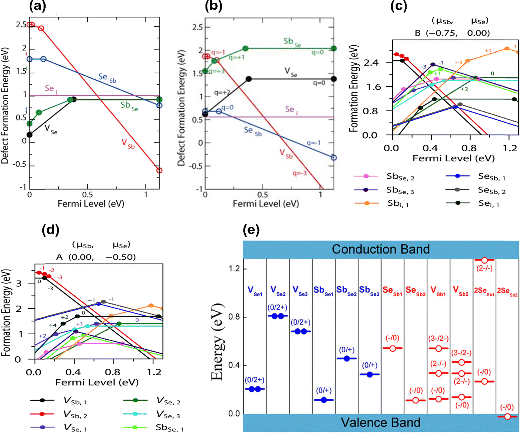 | ||
| Fig. 5 The calculated formation energy of point defects in Sb2Se3 as a function of the Fermi level under (a) Se-rich condition and (b) Se-poor condition.78 Defect transition-level diagrams for Sb2Se3 under limiting chemical potential conditions (c) Se-rich condition and (d) Se-poor condition, plotting defect formation energy (eV) against the position of the Fermi level above the VBM.75 (e) Transition energy levels of intrinsic defects in the bandgap of Sb2Se3. Red-colored levels and blue-colored levels indicate acceptor-type and donor-type defects, with their possible ionization states written above.30 | ||
Similarly, under Se-rich conditions, the Sei defect was predicted via DFT to be present in high concentrations.75,78 However, the ionization level of Sei is above the CBM, and it does not induce any transitional levels in the bandgap (Fig. 5(e)). Therefore, Sei influence on the PV performance is not significant and does not contribute to the carrier concentration or act as a non-radiative recombination center.78 In contrast, Savory et al. showed Sei has multiple transition levels deep within the band gap that could plausibly act as hole or electron traps (Fig. 5(c)).75 This is contradiction to DFT calculations, showing the importance of corroborating theoretical findings with experimental results. It also predicted that under a Se-rich environment, VSb acts as an acceptor with transition levels lying 0.15 eV above the VBM at a neutral state, and when ionized, the Fermi energy shifts to the CBM vicinity (Fig. 5(a) and (e)).30,75 The formation enthalpy of VSb becomes negative as the Fermi level approaches the CBM, thus limiting the Fermi level rising further. Thus, observed p-type conductivity cannot result from VSb. In addition, donor defects VSe2 and VSe3, produce at deep levels in the band gap and act as effective recombination centers for Sb2Se3.30,84 The acceptor defects SeSb2 and 2SeSb2, which have lower formation energies and produce higher concentrations of hole carriers, make undoped Sb2Se3 thin films intrinsically p-type under Se-rich conditions.
| Se-rich | Se-poor | |||||||
|---|---|---|---|---|---|---|---|---|
| Defect | Type of defect | Formation energy (eV) | Activation energy (eV) | Ref. | Type of defect | Formation energy (eV) | Activation energy (eV) | Ref. |
| SeSb | Shallow acceptor | 0.60 | E VBM + 0.12 | 78 | — | >1 | — | 78 |
| Amphoteric | <1.5 | E VBM + 0.69 | 75 | |||||
| Acceptor | <1 | E VBM + >0.40 | 30 | |||||
| 2SeSb | Shallow acceptor | — | — | 30 | ||||
| Sei | Shallow acceptor | 0.60 | — | 78 | — | >1 | — | 78 |
| SbSe | Donor | — | E VBM + 0.49 | 75 | Deep donors | <1 | E CBM − 0.77 | 78 |
| Deep donor | <1 | E CBM − 0.30 | 30 | |||||
| Amphoteric | <1.5 | E VBM + 0.58 | 75 | |||||
| VSe | Donor | 1.1 | VSe1: EVBM + 0.20, VSe2: EVBM + 0.80, VSe3: EVBM + 0.65 | 30 and 84 | Deep donors | <1 | E CBM − 0.74 | 78 |
| Deep donors | <1.5 | E VBM + 0.58 | 75 | |||||
| Deep donor | <1 | E CBM − 0.30 | 30 | |||||
| VSb | Deep acceptor | >1.5 | E VBM + 0.62 | 75 | ||||
| Sbi | Donor | <1.5 | — | 75 | ||||
DLTS measures the activation energy for carrier emission from a defect (Fig. 6(a)). In DLTS spectra, positive peaks represent minority-carrier traps corresponding to electron traps, while negative peaks indicate hole traps. In both cases, two hole traps and one electron trap appeared in similar positions, albeit with different densities. Considering VTD, two hole traps at energy levels of 0.48 eV and 0.71 eV above the VBM occurred, while an electron trap was identified at 0.61 eV below CBM (Fig. 6(b)). That study attributed hole traps (acceptor defects) to VSb and SeSb, whereas electron traps (donor defects) corresponded to SbSe. Meanwhile, Sb2Se3 solar cells fabricated by RTE also display the same point defects corresponding to VSb and SeSb at 0.49 eV and 0.74 eV from VBM and SbSe with 0.60 eV below the CBM (Fig. 6(c)). These results are consistent with the DFT results of Savory et al.75 VTD-Sb2Se3 films have proved to have a reduced trap concentration of 1014 cm3 (compared 1015 cm3 in RTE-Sb2Se3 films) and a long carrier lifetime of 1339 ps (compared 1149 ps for RTE-Sb2Se3 film). Moreover, VTD films were shown to form SeSb and SbSe in similar defect densities (SeSb; NT = 1.1 × 1014 cm−3 and SbSe; NT = 2.6 × 1014 cm−3). This shows the possibility of the formation of SbSe and SeSb antisite defect pairs in Sb2Se3 films, presumably forming [SbSe + SeSb] defect complexes. Thus, complex defect pairs would influence the shift of quasi-Fermi levels, cause serious non-radiative recombination, and lessen the VOC and device efficiency.30,39,55 DLTS showed that the activation energy of SbSe in p-type samples lays between 0.50–0.65 eV,91 which is higher than those predicted by DFT.77 In TAS analysis, three defect levels within the bandgap were detected for Sb2Se3, ranging from 0.2 to 0.6 eV.90,92 Hu et al. systematically analyzed three defects located in the ranges of 0.3–0.4 eV, 0.2–0.6 eV, and 0.5–0.6 eV above the VBM, which were indicated as D1, D2, and D3, respectively90 using temperature dependent TAS. However, TAS analysis failed to distinguish the nature of these defects, (i.e., electron or hole traps). This serves as a good example of where DFT calculations could be better utilized to explain the experimental results.
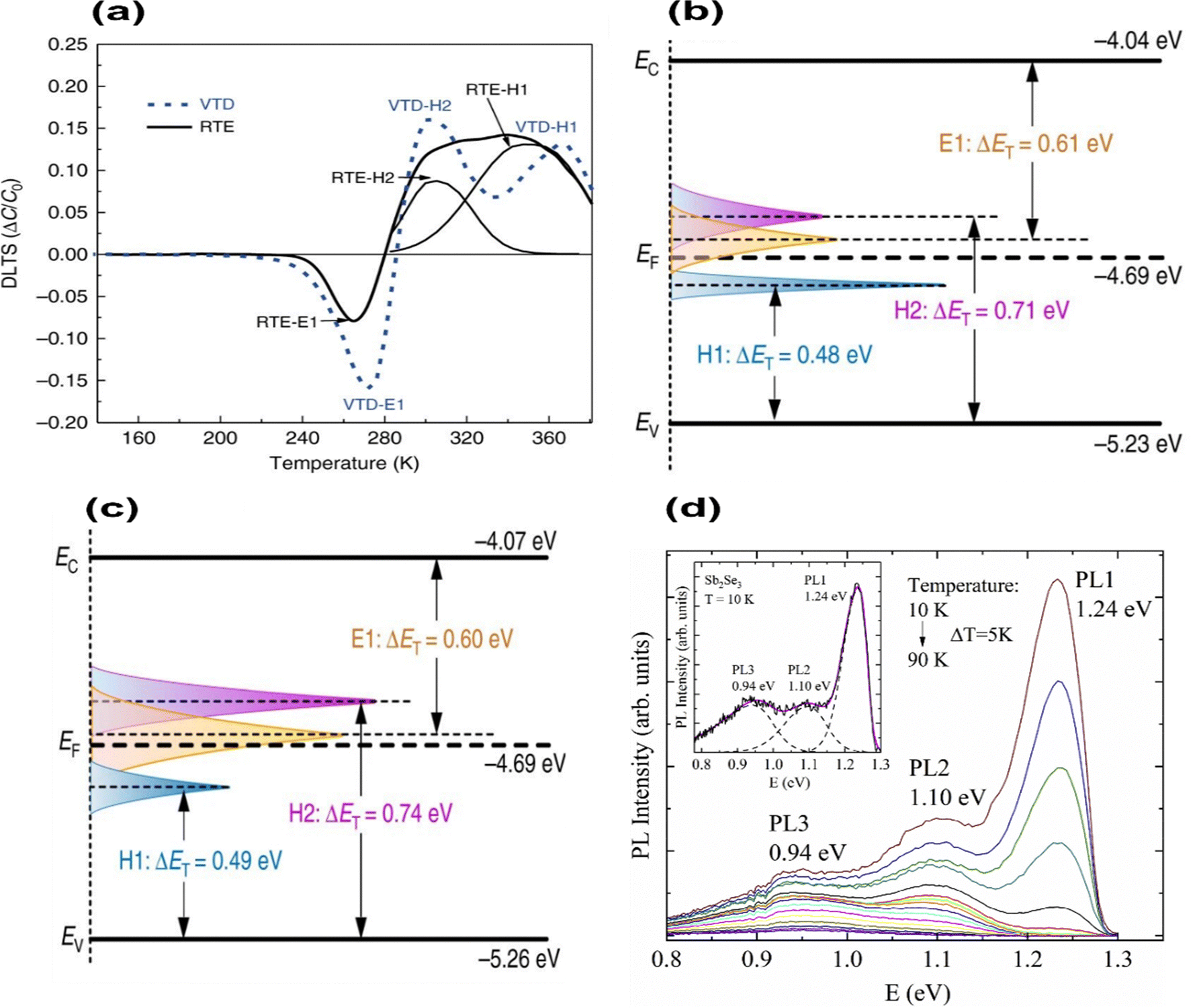 | ||
| Fig. 6 Schematic of the band structure of (a) DLTS signals of VTD-fabricated and RTE-fabricated devices, (b) VTD fabricated Sb2Se3 films, and (c) RTE fabricated Sb2Se3 films (conduction band (EC), valence band (EV), Fermi level (EF), and trap energy level (ET)).39 (d) Temperature dependence of the PL spectrum of Sb2Se3 polycrystals.81 | ||
Furthermore, TAS analysis determined a single defect state presiding with activation energy of 0.095 eV in RTE fabricated Sb2Se3 films with NT of 1.3 × 1015 cm−3. In contrast, temperature-dependent conductance analyzed two defects with activation energies of 0.578 eV and 0.111 eV.7 Accordingly to theoretical calculations, defects with the lowest activation energy of 0.111 eV are ascribed to the SeSb.30 This shows that SeSb is a shallow acceptor with a defect depth of 0.1 eV above the VBM, and thus contributes to p-type conductivity in films. On the other hand, similar to Liu et al.78 Zeng et al. reported that VSe is an n-type donor that effectively reduces the p-type conductivity but also behaves as a recombination center for the photo-generated carriers on films.16 This makes it important to control the formation of VSe to enhance solar cell performance. A study by Grossberg et al. identified three bands at 0.94, 1.10, and 1.24 eV with small thermal energies of 0.033, 0.065, and 0.093 eV, respectively (Fig. 6(d)).81 The PL bands at 1.24 eV and 0.94 eV were thought to originate from donor–acceptor defect pair recombination.93 The 1.24 eV band results from more distant donor–acceptor pairs (shallowest single acceptor defect SeSb formed at a depth of about 0.1 eV). The 0.94 eV band originates from deep donor–deep acceptor recombination, where the donor and acceptor defects occupy the closest Se and Sb sites in the lattice (Sb1–Se3 sites). The third PL band at 1.10 eV is proposed to be related to the GBs; still, further studies are needed to clarify the recombination model.81 The intrinsic defect information of Sb2Se3 obtained using various detection techniques is listed in Table 2.
| Analysis method | Defect type | Assignment | Activation energy (eV) | Defect concentration (NT) [cm−3] | PCE [%] | Ref. |
|---|---|---|---|---|---|---|
| Conductivity | Hole trap | SeSb | 0.111 | 1.3 × 10¹⁵ | — | 7 |
| — | — | 0.578 | — | |||
| Conductivity | Donor | SbSe or VSe | 0.308 | — | 2.92 | 78 |
| — | — | 0.518 | — | |||
| DLTS | Hole trap | VSb | 0.480–0.490 | 1.2 × 10¹⁵ | 7.60 | 39 |
| Hole trap | SeSb | 0.710–0.740 | 1.1 × 10¹⁴ | |||
| Electron trap | SbSe | 0.600–0.610 | 2.6 × 10¹⁴ | |||
| DLTS | Hole trap | VSb | 0.480 | 6.1 × 10¹⁴ | 5.40 | 32 |
| Hole trap | SeSb | 0.710 | 1.0 × 10¹⁵ | |||
| Electron trap | SbSe | 0.630 | 6.5 × 10¹⁴ | |||
| DLTS | Electron trap | VSe2 | 0.390 | (0.98–1.10) × 1014 | 5.60 | 36 |
| SeSb1 or VSb1 | 0.460 | (4.15–8.71) × 1014 | ||||
| VSb2 | 0.690 | (1.18–2.61) × 1015 | ||||
| TAS | — | — | 0.350 | 1.9 × 10¹⁴ | 5.74 | 94 |
| — | — | 0.440 | 6.7 × 10¹⁴ | |||
| — | — | 0.610 | 3.3 × 10¹⁵ | |||
| TAS | — | — | 0.490 | 2.2 × 10¹⁴ | 5.91 | 92 |
| — | — | 0.350 | 1.1 × 10¹⁵ | |||
| — | — | 0.530 | 2.5 × 10¹⁵ | |||
| TAS | — | Bulk defects | 0.360 | 2.2 × 10¹⁴ | 7.50 | 95 |
| — | Bulk defects | 0.390 | 6.1 × 10¹⁴ | |||
| — | Interfacial defects | 0.430 | 7.0 × 10¹⁵ | |||
| TAS | Donor defects | VSe | 0.450 | 9.3 × 10¹⁵ | 6.06 | 41 |
| Donor defects | SbSe | 0.490 | 2.1 × 10¹⁶ | |||
| TAS | Shallow acceptor | VSb | 0.180 | 8.6 × 10¹⁵ | 6.15 | 96 |
| — | Sei | 0.530 | 4.3 × 10¹⁶ | |||
| — | SeSb | 0.570 | 2.5 × 10¹⁶ | |||
| TAS | Hole trap | Bulk defect | 0.286 | 2.4 × 10¹⁴ | 5.91 | 90 |
| Hole trap | Bulk defect | 0.188 | 1.3 × 10¹⁵ | |||
| Hole trap | Interface defect | 0.570 | 1.2 × 10¹⁶ | |||
| PL | — | — | 0.330 | — | — | 81 |
| — | — | 0.650 | — | |||
| — | — | 0.930 | — |
Overall, studies show that defect properties of the atoms on non-equivalent sites are quite different, and defect tolerance changes significantly when the defect gets ionized in different environments. Intrinsic deep defects have a lower concentration under Se-rich conditions than in Se-poor conditions, which results in longer minority carrier lifetime, and better p-type conductivity. Thus, much better PCEs can be achieved for the devices grown under Se-rich conditions. Notably, there is a difference in defect analysis between theoretical and experimental calculations. Compared to theoretical studies, only three defects were found in the DLTS, TAS, and PL experiment analysis in each Sb2Se3 film. This is because theoretical calculations consider all possible sites and different charge states for each defect, whereas experimental methods only probe deep-level defects in the depletion region. As a result, defects that cannot be activated or ionized at room temperature or shallow-level defects are not observed. Therefore, utilizing experimental techniques often leaves significant ambiguity on which specific defect give rise to a specific signal (e.g., SbSe or VSe for Se-poor conditions), whilst also crucial as it only observes the most detrimental defects. Once more, this stress the importance of the combination of computational and experimental analysis.
2.2. Extrinsic defects
Extrinsic point defects can be intentionally or unintentionally introduced during the fabrication of Sb2Se3 films. Controlling unintentional impurities is essential in solar cell fabrication as many common metal contaminants are detrimental to the PCE owing to their deep defect levels.97,98 The impurities/dopants can preferentially reside in substitutional sites, replacing atoms on the crystal lattice, interstitial sites or GBs.70,99 The location of these new defects within the absorber depends on dopant or impurity atomic radius, charge, and bulk crystal structure. The introduction of a dopant can induce changes to carrier density and charge carrier nature in the absorber layer, change the state of intrinsic bulk defects, or introduce new extrinsic defects. These dopants can remain as isolated point defects or join with intrinsic defects to form defect complexes leading to more significant charge traps and defects like planar faults and voids. Under some circumstances, doping-related defects occur within the band gap in large enough concentrations to outnumber native intrinsic point defects and affect the electronic properties of the absorber. Depending on the conductivity properties, dopants can be characterized either as n-type or p-type. Different ratios of doping affect the band offsets of the absorber to form a n–p or n–i–p junction, i.e., sufficient doping density is known to produce bandgap bending at the interface and slightly reduce the amplitude of the interface recombination.55,59 A doping density of 1013 cm3 for RTE fabricated Sb2Se3 films (lower than that of CdTe at 1014 cm3) and effective doping strategies with shallow depth, and small capture cross section are required for substantial improvement of hole densities or electron densities.7,35 But, effective p-type doping is fundamentally difficult in Sb2Se3 due to the presence of insufficiently shallow intrinsic point defects such as VSb and SeSb.30,100 Moreover, extrinsic dopants preferentially enter into interstitial sites between ribbons rather than into the matrix, where dopants are largely inactive or act as donors leading to low p-doping efficiency and thus a low hole concentration.101–106 Therefore, the effective influence of the dopants on electrochemical properties of the Sb2Se3 is ambiguous, and an in-depth understanding of the mechanisms aligned with the physicochemical properties of each type of defect/defect pair is critical to interpreting the improvement of Sb2Se3 thin film solar cells.Under Se-rich conditions, both extrinsic donor Cui and extrinsic acceptor CuSb1 defects were stable.76,107 The formation energy of CuSb1 is lower than that of CuSb2 and CuSb1, and defects formed at a transition level of 0.25 eV above the VBM. They claim that the deep level defect CuSb1 compensated the formation of defects at high concentrations. Competition between the CuSb1 and Cui tends to move the Fermi level to 0.13 eV above the VBM at room temperature, allowing significant improvement of the p-type conductivity. On the other hand, in a Se-poor environment, Cui has a much lower formation energy (0.75 eV) than CuSb (1.46 eV) and a Cui donor defect formed 0.37 eV below the CBM.107 Stoliarof et al. claim that electronically active levels are unambiguously too deep to induce any n-type doping of the absorber at room temperature.76 Moreover, the formation of Cui was compensated by the SbSe a comparable amount, and due to this conflict, the Fermi level shifted to 0.22 eV above the VBM at room temperature, resulting in a slight enhancement of p-type conductivity. However, Chen et al. experimentally showed that n-type doping after copper chloride (CuCl2) chemical bath is due to formation of Cui defects in high concentrations under Se-poor environment.107
2.3. Interfacial defects of antimony selenide thin film solar cells
The discussion so far has focused on defects formed in the bulk of the material. However, interfacial defects formed between the Sb2Se3 film and the transport layers, are also present and deserve a separate discussion. Interfacial defects of Sb2Se3 solar cells have been studied by C–V and DLCP; however, substantial understanding of the origin of interfacial defects of Sb2Se3 is still lacking.109 In addition, the interfacial band alignment of each layer has been measured by ultraviolet photoelectron spectroscopy (UPS).41,67,110 However, in non-pristine non-ultra-high vacuum conditions, the interfacial band alignment is largely affected by the interfacial defects and interfacial band bending. Therefore, direct measurement of chemical state variation at interfaces and band alignments with advanced techniques such as high-resolution photoemission spectroscopy (HRPES) and XPS are required.24,111,112 An ideal buffer layer should yield proper band alignment with a minimum conduction band offset (CBO), which enables stronger photocarrier transport and suppresses lattice mismatch and carrier recombination at the buffer/Sb2Se3 interface. Cadmium sulfide (CdS), zinc oxide (ZnO), and titanium dioxide (TiO2) are the widely adopted buffer layers for Sb2Se3 solar cells, and the CBO has been reported for buffer/Sb2Se3 pairings by several groups.18,19,113 The HRPES determined CBOs of CdS, ZnO, and TiO2 with Sb2Se3 form a spike-like (positive band offset) with 0.24 eV, cliff-like band alignment with −0.11 eV (negative band offset), and nearly a flat band alignment with no distinct transition layers (0 eV) respectively (Fig. 7).111 On the contrary, Li et al. claimed that CdS/Sb2Se3 was a −0.09 eV cliff-like layout.23 Further, CBO and valence band offset (VBO) determined by XPS revealed a spike of 0.25 eV and a cliff of 1.02 eV, respectively.114 This shows that empirical results were inconsistent with one another, and this might be due to the variations in the surface quality of the absorber and different junction formation processes in solar cells (superstrate and substrate), making it difficult to accurately determine the band bending near the surface of the absorber. Furthermore, more advanced characterization techniques to directly measure the CBO value are required to fully identify the CBO loss.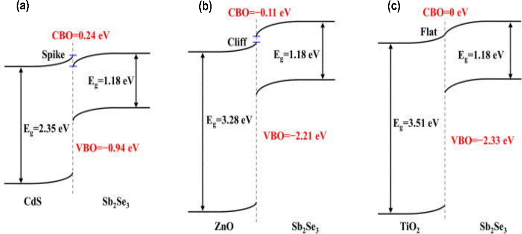 | ||
| Fig. 7 Schematics of the band alignments between Sb2Se3 and different buffer layers (a) CdS, (b) ZnO, and (c) TiO2.111 | ||
Although high PCE values for Sb2Se3 solar cells with CdS buffer layers have been achieved, absorption loss in the short wavelength region, and Cd/Sinterdiffusion into Sb2Se3 film are identified as the main drawbacks. S diffusion was found to be dominant over Cd diffusion, which is responsible for the severe device degradation, causing interfacial defects (e.g., SeS and SSe). Furthermore, replacing Sb3+ sites with Cd2+ ions was found to decrease the p-type conductivity of Sb2Se3. Thus, several groups focused on modifying the CdS buffer layer by including doping, surface treatments, or substituting with appropriate alternatives to improve band alignment with device stability. Learning from CdTe solar cells,115 doping of the CdS layer by replacing some Cd or S atoms with oxygen (O2) was applied to Sb2Se3 solar cells.29 Notably, the introduction of n-type O2 was found to improve the n–p junction quality by suppressing the carrier recombination at the absorber/Sb2Se3 interface. Moreover, doping of the buffer widens the band gap of the CdS and tunes the energy alignment from “cliff” like to “spike” like.29 Similarly, Guo et al. reported accumulation of the O2 at the CdS:O/Sb2Se3, significantly suppressing interfacial diffusion of Cd and formation of n-type Cdi.116 With a trace amount of Cl and more O, the surface defects on CdS grains were passivated, reducing the ideality factor (A) from 2.70 to 2.16 and the reverse saturation current density (J0) from 0.09 mA cm−2 to 0.02 mA cm−2 in CdCl2 treated devices compared to a control device.117 Furthermore, ambient storage of films decreases the A from 2.2 to 1.9 and the J0 from 9.0 × 10² mA cm−2 to 8.7 × 10³ mA cm−2, exhibited reduced recombination loss or equivalently improved transmission and junction quality.67 The isotropic O2 diffusion into Sb2Se3 was found to tailor the (Sb4Se6)n ribbons to a [221] textured orientation, forming Sb–O–Se chains or SbSeOx compounds, which can fill the van der Waals gap between the Q1D ribbons.118 This demonstrates that O2 provides a unique pathway to engineer the morphology, interface quality, electrical and optical properties as well as performance of Sb2Se3 solar cells.116,118 Combined analysis of C–V and DLCP characterization stated thermally evaporated Sb2Se3 films contain interfacial traps of 1016 cm3 while Se compensated films contain reduced traps of 1015 cm3. This revealed Se interfacial defect passivation by Se compensation is an effective method compared to O2 treatment during film evaporation. However, defects associated with O, Cd, S, Sb, and Se needed to be thoroughly evaluated for the future development of PVs.
Wang et al. showed substrate temperature and annealing duration of ZnO produced by spray pyrolysis plays a decisive role in the crystal orientation of Sb2Se3.19 It was noticed that [001]-oriented ZnO results in higher interfacial defect density of 3.77 × 1011 cm−2 than random orientated ZnO (1.22 × 1011 cm−2). Consequently, the growth of [221]-oriented Sb2Se3 films is not thermodynamically feasible on the [001] plane of ZnO due to dangling bonds and poor film adhesion. Conversely, randomly orientated ZnO always promotes [221] orientation of Sb2Se3 grains.
Recently, many literature reports have revealed that desired crystal orientation with higher PCEs have been achieved in both superstrate and substrate Sb2Se3 solar cells using TiO2 as a buffer layer.9,20,113,119 Kondrotas et al. revealed that bonding of Sb and Se with the TiO2 substrate during the film deposition is difficult due to higher Ti–O bond energy (662 kJ mol−1) than Cd–S (196 kJ mol−1). This means that when CdS is used, most of the (Sb4Se6)n chains lying on the substrate leading to [120] oriented ribbons,20 and in the formation of dangling bonds and interfacial and GB defects resulting in poor PCE and higher VOC deficit. Therefore surface/interface modifications are needed to enhance PCEs.
3. Recombination processes and carrier transport in antimony selenide thin film solar cells
A typical thin-film Sb2Se3 solar cell usually consists of a front contact, window layer, buffer layer, absorber layer, and back contact.1,3 As a result, the overall performance of the solar cells is not only governed by the quality of the absorber layer but also the properties of other layers and interfaces. As described in Section 2.3, the defect states present in the interfaces between the absorber and transport layers are incredibly complicated and lead to carrier recombination and severe VOC deficit.1,3,55 For solar cells, the main carrier recombination pathways include radiative recombination (photons), Auger recombination (electrons), and defect-assisted recombination. Compared to other thin-film PVs, it was recently reported that Sb2Se3 devices exhibit weak Auger recombination such that it has a negligible influence on their performance.30,78 These recombination pathways are identified to take place at different sites within the heterostructure, namely at the absorber surface, in the absorber bulk, at the absorber back contact, in the absorber space charge region (SCR), in the buffer layer, and finally in the window layer (Fig. 8).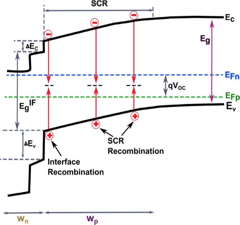 | ||
| Fig. 8 Schematic presentation of the possible recombination paths of heterostructure Sb2Se3 solar cells under open-circuit conditions (where Ec, Ev, Eg, EIFg, wn, wp, and EFn/EFp are denoted by the conduction band, valence band, bandgap, interface bandgap, width of the SCR in the buffer layer, width of the SCR in the absorber layer, and quasi-Fermi levels respectively). | ||
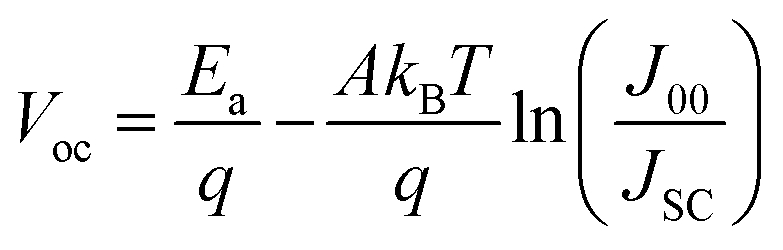
When an active defect state energetically lies within the bandgap, it frequently captures or traps an approaching electron or hole, whereas when energy levels are shallow enough, the trapped carrier can escape through thermal energy. Under steady-state conditions, the detailed balance of carrier generation and recombination processes determines the performance of PV devices. Yet measuring the energy associated with each defect practically becomes difficult under open-circuit conditions. To understand the interface–induced recombination process and large VOC deficit following equation is used.3,37,59
The carrier recombination mechanism in Sb2Se3 solar cells can be identified by the A and the activation energy at 0 K.3,55Table 3 summarizes the reported A or activation energy of Sb2Se3 solar cells in the literature. When all the parameters of Sb2Se3 are well optimized, the A values of devices are found to be between 1 and 2, indicating that interface recombination is dominant, and SCR recombination may concomitantly participate in Sb2Se3 solar cells when A is closer to 2.94,120 In theory, if the bandgap is equal to or lower than the recombination activation energy, Shockley–Read–Hall (SRH) recombination in the SCR or neutral region of the absorber will dominate over interface recombination.3,59 The activation energy of interface and SCR recombination in Sb2Se3 solar cells is lower than the band gap, which is well in line with statistical results in Table 3 and implies that the interface–induced recombination dominated over SCR recombination and contributes to the J0.3,55,59
To gain further insight into the specific influence of each defect on the carrier dynamics and defect density states of the absorber, TRTA, time-resolved photoluminescence (TRPL), terahertz (THz) spectroscopy, and angular frequency-dependent capacitance were employed.7,39,72,79,80,123 The activation energy of the dominant defects (VSb and SeSb) of Sb2Se3 is much larger than that of Sb2S3 and kesterite materials,78 which means that only 2.6% of the bulk defects of Sb2Se3 contribute to the free carriers, leading to low free carrier density (7.7 × 1013 cm−3), limited bulk conductivity, and small quasi-Fermi level splitting under illumination. The NT values of 6.9 × 1014 cm−3 and 1 × 1015 cm−3 were determined from space charge limited current measurement and first-principle calculation for Sb2Se3 films at room temperature, respectively.78,121 The same NT of 1 × 1016 cm−3 eV−1 and an integrated NT of 1.3 × 1015 cm−3 were detected by TAS.7 From these studies, NT in Sb2Se3 was confirmed to be in the range of 1014–1016 cm−3, and this value is 1–3 orders of magnitude greater than that of CdTe and CIGS solar cells, implying significantly more disorder in Sb2Se3 films.3 Furthermore, conductivity measurements taken from temperature-dependent dark conductivity show that Sb2Se3 films follow two different electrical conduction mechanisms.7,80 Above 160 K, the electrical conductivity in films depends on the number of thermally activated carriers ionized from shallow defects over the inter grain potential barriers. Chen et al. showed intrinsic excitation dominates the carrier density from 250–420 K, and the activation energy (0.578 eV) is found to be half of the direct bandgap of Sb2Se3. On the other hand, at low temperatures (85–60 K) conductivity was reduced with the temperature as the conduction mechanism changed into Mott's variable range hopping between localized states in the bulk of the grains.7,80
Due to the presence of a large quantity of effective recombination centers at the interface originating from mismatched or imperfect energy level alignment to the energy barrier with the back contact, interdiffusion, and segregation of impurities, the rate of interface recombination is greater (τ1, shorter carrier lifetime) than that of SCR recombination (τ2, longer carrier lifetime). It has been found that a short lifetime of 0.1–1 ns (i.e., interface/surface recombination)79,124 and a long lifetime of 5–60 ns (i.e., bulk defect recombination) (Table 4)7,72,79 were commonly observed in Sb2Se3. These results revealed that the interface induced lifetime of Sb2Se3 is far inferior to that of traditional absorbers, i.e., CdTe (∼3.6 μs), CIGS (∼250 ns), and CZTS (∼10 ns)3,79 due to a large capture cross-section, high density, and deep energy levels. In particular, Wang et al. revealed the surface recombination velocity of 2 × 103 cm s−1, which is much greater than that of CdTe (1.2 cm s−1).79
| Analysis method | Fabrication method | τ 1 (ns) | τ 2 (ns) | Ref. |
|---|---|---|---|---|
| TRTA | RTE | — | 67 | 7 |
| TRTA | VTD | 1.339 | — | 39 |
| TRTA | RTE | 1.149 | — | 39 |
| TRTA | Solution | 0.01 | 5.25 | 32 |
| TRPL | Solution | 0.15 | 0.61 | 124 |
| TRPL | Solution | 0.13 | 0.32 | 124 |
| TRPL | Solution | 0.12 | 0.26 | 124 |
| Calculation | VTD | — | 21 | 90 |
| Calculation | Sputtering | — | 1–64 | 72 |
| TA | Thermal evaporation | — | 37.2 | 78 |
| TA | Thermal evaporation | 0.023 | 79 | |
| THz | Solution | 0.03 | — | 124 |
| THz | VTD | 0.003–0.005 | 0.04 | 123 |
| THz | Thermal evaporation | 0.023 | 79 |
Therefore, for reasonable carrier mobility and high electrical conductivity, carrier transport materials with proper band alignment, a minimum CBO and lower lattice mismatch are essential. To this end, wide-band gap buffer layers (CdS, ZnO, TiO2, etc.) have been selected to improve the device performance, but the rises are often rather modest.18,19,38,92,113,117,125–128 Furthermore, inorganic hole transport materials (HTM) such as NiO2,129 WO3,130 MnS2,131 and organic HTMs like PCDTBT,9 (PCPDTBT),52 spiro-OMeTAD,32 CZ-TA,45 and P3HT132 have been introduced to enhance carrier extraction, passivate back contact defects and mitigate pinholes, but improvements in VOC and PCEs are modest. Therefore, more suitable buffers and HTMs with high stability, low cost, low toxicity, matched energy level alignment, lower lattice mismatch, and simple preparation processes are needed to suppress the interfacial recombination and promote efficient carrier transport.
4. Extrinsic doping approaches
Absorber doping is a widely explored method to tune the thermoelectrical and photoelectrical properties of semiconductors by bandgap modulation,133,134 improving film conductivity, increasing carrier concentration,135,136 improving photoactivity,33,137 increasing grain size,138 regulating crystallization or morphology,103 and passivating surface or grain boundaries.107 Dopants can occupy the surface, GBs, or in the lattice by replacing host atoms and interstitial sites in the crystal structure, and these can either be isovalent or heterovalent. Cations with large diffusion coefficients and low diffusion barriers (e.g., Cu2+, Te2+, Pb2+, etc.) have been recognized as preferred dopants in Sb2Se3 thin films for solar cells.32,105,107,139 Despite the fact that both Sb2Se3 and Sb2S3 have similar Q1D structures, doping strategies used in Sb2S3 have been reported to be similar compared to Sb2Se3.58,140Table 5 summarize advances that have been made in the doped Sb2Se3 thin films solar cells and effect of dopants in Sb2Se3 absorber for thin films solar cells are discussed below.| Dopant | Doping method | Doping concentration [at%] | Carrier concentration (cm−3) | Doping type | Doping position | Ref. |
|---|---|---|---|---|---|---|
| Sn | Melt quenching | 0.1 | 1.94 × 10¹⁶ | p-type | In the lattice | 99 |
| Fe | Electro deposition | 5 | 1.0 × 10¹⁹ | p-type | In the lattice | 139 |
| Fe | Hydrazine solution process | 0.1 | 3.4 × 10¹³ | n-type | In the lattice | 106 |
| Pb | Magnetron sputtering | — | 1.7 × 10¹³ | p-type | In the lattice | 143 |
| I | Magnetron sputtering | 0.1 | — | n-type | In the lattice | 44 and 68 |
| Cl | Unintentional doping from starting materials | — | 1016–1017 | n-type | — | 108 |
| Cu | CuCl2 treatment | — | — | n-type | GBs | 107 |
| Te | Thermal evaporation | 0.08 | — | — | In the lattice | 71 |
| Te | Magnetron sputtering | 0.03 | — | n-type | In the spacing of (Sb4Se6)n ribbons | 70 |
| Te | Spin coating | 2.2 | — | n-type | GBs | 32 |
| Lanthanides | Co-reduction method at hydrothermal condition | 0.04 | — | — | In the lattice | 148 |
| S | Spin coating | 5.34 | — | — | — | 32 |
| Mg | Hydrazine solution process | 0.1 | 5.1 × 10¹³ | — | GBs or GIs | 106 |
| Na | Thermal evaporation | 0.2 | — | — | GBs or GIs | 101 |
4.1. Tin doping
Chen et al. reported a systematic study on Sn doping of Sb2Se3 films using the conventional melt-quenching method in vacuum sealed silica tubes.99 Pure Sb2Se3 exhibits a low conductivity of 2.71 × 10⁻⁶ S cm−1, and the conductivity of Sn doped Sb2Se3 was found to increase with increasing Sn content reaching higher conductivity of 7.50 × 10⁻² cm−3 at 0.1 at% of Sn. Incorporation of Sn was found to convert n-type pristine Sb2Se3 films to p-type. Thus, suggesting that Sn4+ replaces the Sb3+ ions in the Sb2Se3 matrix and as Sn4+ possesses two fewer valence electrons, it acts as a hole donor at the doped site and therefore enhances the electrical conductivity, resulting in bulk charge-carrier density from 1.44 × 1011 cm−3 (x = 0.00) to 1.94 × 1016 cm−3 (x = 0.10). As a result of doping, dark current density increased from −16 μA cm−2 to −160 μA cm−2 at a bias voltage of −0.6 V, and the photocurrent density increased from −18 μA cm−2 to −250 μA cm−2 at −0.6 V. Interestingly, pristine Sb2Se3 shows a direct band gap of 1.17 eV and Sn doping narrow band gap to 1.10 eV. The authors discussed narrow band gap absorber with specific doping levels is due to the Burstein–Moss shift and the renormalization effect.141,1424.2. Iron doping
Iron (Fe)-doped Sb2Se3 films grown by electrodeposition have been studied by Costa et al.139 The study showed that 5 at% Fe doping increases the carrier density from 1.0 × 1019 cm−3 for undoped Sb2Se3 to 3.7 × 1016 cm−3 for doped Sb2Se3, which then exhibits p-type conductivity. However, doped Sb2Se3 presented a similar photocurrent density (165.13 μA cm−2) to that of undoped films (166.34 μA cm−2) and further shows that Fe has a low influence on band gap and morphological properties of the films. It should be noted that this is true despite an extremely high doping concentration of the films. Furthermore, Li at el. also showed that Fe doped Sb2Se3 has increased carrier mobility from 9.0 cm2 V−1 s−1 to 14.2 cm2 V−1 s−1 with negligible change in carrier concentration (4.9 × 1013 cm−3 in pristine Sb2Se3 and 3.4 × 1013 cm−3 in Fe doped-Sb2Se3).106 However, in contrast to Costa et al.,139 Kelvin probe force microscope and Hall measurements revealed that Fe doping changes poor p-type Sb2Se3 thin-film to n-type. This significant discrepancy is likely to arise from the different defect types and their interactions in the two experimental environments.4.3. Lead doping
Pb-doping in Sb2Se3 has been studied by Li et al. with an unspecified amount of dopants in the form of lead iodide (PbI2).143 Their experiments showed that Pb doping enhances the hole concentration from 1.6 × 10⁹ to 1.7 × 1013 cm3 and VOC from 0.32 to 0.38 V, and the PCEs from 2.87% to 4.43%, indicating that PbI2 is an effective p-type dopant. Although the hole concentration increased, the mobility decreased from 18.7 to 1.3 cm−2 V−1 s−1, which may be due to deterioration of crystal quality, ionized impurity scattering, phonon scattering, and GB scattering originating from PbI2. TA spectra show that PbI2 also passivates the GBs and suppresses interface recombination. Furthermore, this study showed that doping of lead as Pb0 metal showed no doping effect on Sb2Se3, which hints that Sb3+ is likely to be replaced by Pb2+ in the crystal structure.4.4. Halide doping
I doping into Sb2Se3 by sputtering was carried out in two separate studies which suggest that I is an effective n-type dopant.44,68 Ren et al. indicate that I successfully occupies the lattice sites of Sb2Se3, however, due to its larger size makes diffusion more difficult and significantly inhibits the growth of Sb2Se3 grains.44 In addition, Chen et al. were able to produce 0.1 at% I doped thin films with an increased photocurrent density of 770 μA cm−2 compared to pristine at 0.7 V after post-heat treatment at 350 °C.68Hobson et al. determined that unintentional Cl doping in purchased Sb2Se3 material acts as a shallow dopant, significantly shifting the Fermi level position, and subsequent Sb2Se3 films are n-type.108 Here Cl doping occurs in both Se-rich and Se-poor conditions. However, in both chemical potential limits, ClSe appears to be the dominant defect due to its low formation energies (<0.5 eV), Cl could easily substitute Se sites. Furthermore, the defects are compensated by VSb below the conduction band edge (0.3 eV), leading to significantly higher carrier concentrations in the range of 1016–1017 cm−3. This demonstrated that in contrast to the standard p–n heterojunction architecture, a novel n–n isotype heterojunction Sb2Se3 solar cell formed at TiO2/Sb2Se3 interface. Further DFT calculations illustrated that with the proper band alignment and higher carrier concentration, the Cl doped Sb2Se3 solar cells can achieve a PCE of 7.3%.108 However, considering the deep-level compensating defects caused by Cl, anion doping is still needed in future research.
4.5. Copper doping
The PCEs of Sb2Se3 are mostly hindered by deep level defect recombination at vacancy defects (VSe) and substitutional defects (SeSb or SbSe). The spatial separation of carriers at deep defect centers creates an electric field between GBs and grain interiors (GIs). As discussed earlier, Sb2Se3 films are often weakly p-type, and the introduction of dopants was found to convert GBs into n-type. This will then lead to the Fermi level difference between GBs and GIs, which induce an electric field from GBs to GIs creating electrons to pass through GBs and holes through GIs. The GB inversion, therefore, restrains the electron–hole recombination. For this process, effective n-type doping has been carried out using metal cation interstitial doping (such as Cu2+) or substitutional doping by halogens (such as I).44,107 The introduction of CuCl2 in aqueous ammonia (NH3) at low temperatures induces the diffusion of Cu2+ ions into Sb2Se3 films along the GBs, as has been utilized extensively for CdTe devices.144 Chen et al. showed that a built-in electric field was established under the addition of Cu2+ between p-type GIs and n-type GBs, forming an interstitial defect (Cui).107 CuCl2 treatment reduces the surface potential of GBs compared to the control sample causing uplift of the Fermi level very close to the conduction band of Sb2Se3, confirming the n-type inversion at GBs. Consequently, spatially separation of photogenerated carriers suppresses nonradiative recombination at GIs, enhances carrier collection, and improves the VOC and JSC of the device. DFT simulations show the origin of the n-type inversion after CuCl2 treatment in Sb2Se3 to be substitutional CuSb (an acceptor, increasing p-type conductivity) and interstitial Cui (a donor, increasing n-type conductivity). Under Se-rich conditions, the formation energies for the two doping sites are both high (>1 eV), whereas in Se-poor conditions, Cui has a much lower formation energy (0.75 eV) than CuSb (1.46 eV), indicating that Cui is easier to form than CuSb.1074.6. Tellurium doping
As mentioned previously, under Se-rich conditions, SeSb and VSb are dominant in Sb2Se3 films and directly affect the device performance.39 Ma et al. demonstrated an effective strategy to remove these acceptor defects in Se-rich Sb2Se3 films by introducing 2.2 at% Te.32 Unlike other metal elements, Te can regulate the atomic ratio of Se/Sb in Sb2Se3 films by competitively reacting with Se to form Sb2Te3-doped Sb2Se3 instead of an Sb2(Se,Te)3 alloy. DLTS analysis showed that pristine Sb2Se3 solar cells displayed three deep traps corresponding to two-hole traps H1 (E = 0.48 eV, NT = 6.10 × 1014 cm−3), H2 (E = 0.71 eV, NT = 1.00 × 1015 cm−3) and one electron trap E1 (E = 0.63 eV, NT = 6.49 × 1014 cm−3) whereas Te doped Sb2Se3 films displayed one hole trap H1 (E = 0.48 eV, NT = 5.34 × 1013 cm−3) and one electron trap E1 (E = 0.64 eV, NT = 3.32 × 1014 cm−3). Typically, the hole traps (acceptor defects) with defect energy levels H1 and H2 are indexed to VSb and SeSb, respectively, and electron traps E1 (donor defects) correspond to SbSe. The pristine Sb2Se3 device delivered a PCE of 3.3%, with JSC of 21.6 mA cm−2, VOC of 312 mV, and FF of 48.2%. Deep level acceptor defects (SeSb) were found to be completely suppressed by 2.21 at% Te-doped Sb2Se3 films, greatly reducing the charge recombination and thus rendering a longer carrier lifetime giving rise to pronounced enhancement in PCEs to 5.4% (JSC 29.0 mA cm−2, VOC 360 mV, and FF 51.5%). Although the work claims to have completely mitigated deep defects in Sb2Se3, the improvement of VOC is not that significant. The film resistivity for the pristine device is recorded as 2196 Ω cm2, while Te-doped device increases to 7843 Ω cm2. The remarkable increase in recombination resistance suggests the 2.21 at% Te doping Sb2Se3 based device prevents charge recombination more efficiently than the pristine Sb2Se3 based device. This reduced recombination probability contributes to the enhancement in VOC and FF of the device. Another study of Te doping in Sb2Se3 solar cells was reported by employing the thermal evaporation technique.71 As compared to the control device without doping, the device with an optimal doping concentration of 0.08 at% showed an unusual increase in optical band gap from 1.46 to 1.65 eV, which was then ascribed to the crystallization of multiple Sb–Se phases with higher bond energies. However, the conductivity of doped films was reduced to 1.22 × 10⁻⁷ Ω−1 cm−1 compared to undoped Sb2Se3 2.55 × 10⁻⁷ Ω−1 cm−1. The authors show the decrease in the conductivity may be due to the reduction in thermal activation energy, which may be due to defects at GBs, voids, and surface imperfections. But a detailed analysis of defects associated with each GB and surface corresponding to the VOC and PCE is not provided. However, an Urbach energy of 0.12 eV recorded for pure Sb2Se3 films and 0.16 eV for 0.08 at% Te doped films, is lower compared to other reported values.55 The Raman spectra prove that the Te inclusion tunned the Se/Sb ratio of Sb2Se3 and formed intermixed alloys such as Sb2Te3-doped Sb2Se3 instead of the Sb2(Se,Te)3 alloy. In addition, the Te doping was found to mitigate the surface oxidation of Sb2Se3 and reduce the optical absorption and absorption coefficient (from 0.89 × 104 cm−1 to 0.75 × 104 cm−1) compared to the pristine Sb2Se3 film, which in agreement with the previous report.145Furthermore, Ren et al. investigated the Te doping in Sb2Se3 by magnetron sputtering.70 This shows that Te atoms were accommodated into the spacing of [Sb4Se6]n ribbons rather than in the lattice and formed n-type Sb2Se3. It was found that post-deposition annealing at 325 °C had a crucial influence on the photocurrent density of films, and a current density of 1.91 mA cm−2 was recorded for annealed films. Moreover, due to the change in atomic arrangement from disorder to ordered structure, the band gap of as-deposited films (1.65 eV) decreased to around 1.27 eV after annealing. Similar to Sn doping, an increase in the band gap with respective to pristine Sb2Se3 thin films (1.15 eV) was attributed to a combination of the Burstein–Moss shift and the renormalization effect, existing in the narrow band gap semiconductor with a certain doping level.141,142
4.7. Lanthanide doping
Alemi et al. have incorporated large electropositive ions, such as the lanthanides (holmium (Ho3+), neodymium (Nd3+), lutetium (Lu3+), samarium (Sm3+), gadolinium (Gd3+), erbium (Er3+), and ytterbium (Yb3+)) into the Sb2Se3 lattice by the hydrothermal co-reduction method.102–104,146,147 However, these studies show that the incorporation of Gd3+ and Sm3+ into Sb3+ sites form a LnxSb2xSe3 structure. This is isostructural with Sb2Se3 and does therefore not change the morphology of Sb2Se3.102 According to differential scanning calorimetry, the electrical conductance of lanthanide-doped materials was enhanced compared to undoped Sb2Se3 at room temperature (i.e., pure Sb2Se3; 0.2 Ω m and Sb1.96Gd0.04Se3: 6 × 10⁻² Ω m).102,147 However, substitution of Sb3+ with Yb3+ and Er3+ leads to morphology changes from nanorods to nanoflowers,103 while Sb2Se3 films co-doped with Lu3+/Yb3+ (Lu0.04Yb0.04Sb1.92Se3) and Lu3+/Er3+(Lu0.04Er0.04Sb1.92Se3) produce nanorods and nanoparticles, respectively. Besides, the electrical resistivity of co-doped Sb2Se3 (0.009 Ω m for Lu3+/Yb3+, 0.032 Ω m for Lu3+/Er3+) is lower than that of the pure Sb2Se3 (0.200 Ω m) and decreased linearly with temperature.148 Therefore, lanthanide doping has been shown to promote the electrical conductivity of Sb2Se3 as well as thermoelectrical conductivity.In addition to the dopants discussed above, alkaline metals such as sodium (Na) and magnesium (Mg), or chalcogenide atoms like S have been used to doped Sb2Se3 films (Table 5).101,106,139 However, segregation of dopants such as Na and Mg into GBs or GIs makes them largely inactive which makes film properties and device performance are independent from the presence of these dopants.76,101 The concentration of dopants inclusive in Sb2Se3 thin films is questionable. Therefore, at higher concentrations of dopants, excess metal dopants were found to be present compared to Se and Sb, which often forms solid solutions or discreet secondary phases instead of doping.149 Therefore, a complete understanding of the absorber-dopant correlation is essential for the future development of PVs.
5. Suppression of defects
Defect modulation at the surfaces and interfaces in Sb2Se3 thin films is a key issue in defect engineering and plays a vital role in modifying the functional properties of the material. The core aspect of defect engineering lies in modulating the concentration and spatial configuration of defects. This mainly depends on the Sb and Se chemical potential during film deposition, substrate modification, post-processing treatment, and interfacial modification. Although great advances have been achieved to mitigate defects, atomic-level understanding of the defect passivation mechanism for different passivators has not been fully explored (i.e., the interaction between GBs/surface defects and passivation techniques). Therefore, it is essential to understand the underlying working mechanism of passivators, which could guide researchers towards an effective passivation strategy for Sb2Se3 and other absorber materials. This section reviews recently reported techniques to suppress defects associated with absorbers that are used to overcome VOC bottleneck and defect-assisted recombination.5.1. Suppressing defects through post-annealing treatment
Post-deposition annealing treatment is one of the most efficient methods to improve film quality via increasing the crystallinity, tuning the crystal orientation, increasing grain size, decreasing porosity, and reducing defect concentration.139,150 Post-annealing treatment on Sb2Se3 films has been carried out in different annealing conditions, i.e., air, vacuum, argon (Ar), nitrogen (N2), and Se vapor.63,94,151 Leng et al. demonstrated that post-annealing of thermally evaporated Sb2Se3 films in a Se atmosphere compensates for Se loss during thermal evaporation and increases the doping density from 1.3 × 10¹⁶–2.4 × 1016 cm3 to 1.7 × 10¹⁶–2.6 × 1016 cm3. This attenuated the VSe associated recombination loss and resulted in improved device efficiency from 1.9% to 3.7%.63 Photoelectrochemical analysis (photocurrent–potential and photovoltage tests) confirmed p-type conductivity for potentiostatic electrodeposited Sb2Se3 films.151 As deposited films showed an optical absorption coefficient of 1.95 × 105 cm−1, and when these films were annealed at 300 °C in Ar atmosphere, the absorption coefficient decreased to 1.61 × 105 cm−1. Authors claimed that higher absorption coefficient of the as-deposited films exhibited due to the poorer crystallinity and higher defect density which then may act as light absorption centers, whereas post-annealing enhances the crystallinity. Photoelectrochemical tests revealed excellent photoelectrochemical activity in annealed samples which is evident in the reduction of defect densities. Furthermore, C–F measurement of post-annealed VTD films at 200 °C in vacuum conditions showed three defect levels at 352, 440, and 606 eV in the bandgap with NT of 1.9 × 10¹⁴, 6.7 × 10¹⁴, and 3.3 × 1015 cm−3 respectively. Whereas unannealed films showed three defect levels but at higher thermal activation energy with higher NT. This shows that NT of the post-annealed sample was lower compared to pristine films, and therefore the net carrier concentration increased from 1.13 × 1017 cm−3 to 1.30 × 1017 cm−3, raising the efficiency from 4.89% to 5.72%.94 However, heat treatment post deposition induced more Cd and S inter-diffusion across CdS/Sb2Se3, demonstrating that there can be negative consequences to post-deposition annealing.34 Post-annealing at 300 °C under an inert environment caused delamination of the antimony oxide (Sb2O3) from the Sb2Se3. However, annealing of Sb2Se3 in the presence of O2 was found to passivate VSe defects leading to lower defect densities and reduced defect energy levels. Five characteristic activation energies at 0.326, 0.446, 0.381, 0.536, and 0.489 eV were obtained for unannealed samples, whereas three activation energy levels were obtained for annealed devices at 0.344, 0.509, and 0.475 eV.119 Furthermore, annealing at higher temperatures such as 400 and 500 °C caused crystallographic texturing of films in the [120] direction, which diminishes its PV properties.139,150 Further, Ma et al. prepared Sb2Se3 thin films by co-sputtering of Sb2Se3 and Se targets with a substrate temperature of 350 °C without a subsequent annealing process, exhibited better crystallinities and a preferred orientation along the [221] direction.1525.2. Suppressing defects through post-selenization treatment
Based on the above results, it has been found that Sb2Se3 films possess donor defects that are difficult to manipulate due to a Sb or Se elemental imbalance. Thermally fabricated Sb2Se3 films were mostly Se poor, in which deep level defects such as SbSe and VSe dominantly act as carrier traps. Therefore, post-selenization or in situ selenium compensation processes are critical to produce films with an optimal elemental ratio (Sb/Se = 0.666) to restrain detrimental intrinsic Se defects related to recombination.30,78 Thus, adjusting the element ratios and passivating the volatilization of chemical components are crucial methods to minimize recombination centers of carriers (electron traps/hole traps) at buffer/Sb2Se3 and HTL/Sb2Se3 interfaces, enhance photoresponse, and increase photocurrent.32,78 Liu et al. further revealed an additional selenization step provides excess Se to compensate for the SbSe and VSe defects that originated from thermal evaporation.78 Two defects were depicted for the as-produced Se-poor Sb2Se3 films at 308 and 518 meV and for Se compensated films (Se-rich) at 107 and 503 meV. It can be shown that defects present in pristine films can be deep donor defects, either SbSe or VSe or both in high concentrations. However, under Se-rich conditions, the defects activation energy of SbSe or VSe are lowered, and SeSb acceptor defects are introduced at 100 meV depth below the CBM.30 The beneficial effects of Se compensation enhanced the photocarrier lifetime up to 102 ns, which is 2.5 times longer than the pristine device. Enhanced photocarrier lifetime was attributed to lower charge recombination loss and improved quality of the CdS/Sb2Se3 heterojunction with lower interfacial and bulk defects leading to a PCE of 5.76% (JSC of 26.3 mA cm−2, VOC of 0.38 V, and FF of 57%). In addition, Tang et al. proposed a post-selenization treatment for magnetron sputtered Sb2Se3.41 This study revealed deposition temperatures can vary the Sb/Se ratio of Sb2Se3 films, that Se-poor films with an Sb/Se ratio of 0.688 were obtained at a selenization temperature of 420 °C and had a minimum defect density of 9.29 × 1015 cm−2 with an activation energy of 456 meV. Moreover, C–V profiling and DLCP suggested a lower interfacial defect density of 1.88 × 1011 cm−2 and a reduction of recombination at the CdS/Sb2Se3 interfaces, increasing the PCE to 6.06% with an outstanding VOC of 0.494 V. Moreover, Liang et al. reported a PCE of 6.84% with an impressive VOC of 0.504 V for Sb2Se3 solar cells prepared by selenization of the sputtered Sb precursor thin films.34 Although a higher VOC was recorded, post-selenization heat treatment induced an insufficient selenization or crystallization of Sb2Se3 films leaving the films Se deficient (Sb/Se ratio of 0.67). Moreover, severe stoichiometric deviations to Se-poor films (Sb/Se = 0.69) are prone to produce defects with high NT of 1.32 × 1016 cm−3 and 1.38 × 1016 cm−3 and activation energy of 310 meV and 407 meV, respectively. Besides, Li et al. revealed that electron beam evaporated Sb followed by selenization at temperatures above 360 °C gradually changes the grains from round shape to rod-like shape introducing some craters and cracks in the films.153 Sb2Se3 films fabricated at 360 °C showed an average grain size of 450 nm, an optical bandgap of 1.24 eV, carrier concentration of 4.99 × 1012 cm−3, and a carrier mobility of 6.88 cm2 V−1 s−1, which are comparable with reported values of Liu et al.67 Selenization of Sb2Se3 films deposited on Mo-coated glass substrates by CSS at 425 °C shows to increase in the grain size (0.87 to 2.68 μm), crystallinity, and improved the orientation of the films, which results in a reduced VSe related recombination loss, particularly at Sb2Se3 ribbon edges and GBs.64 With all these benefits of proper selenization, a significant carrier density of 7.21 × 1016 cm−3 and device performance improvement of 1.85% to 6.43% is achieved. Besides, the selenization treatment also facilitates the formation of a thin MoSe2 layer at the Sb2Se3/Mo interface, which helps to improve the back-interface quality and eliminate the Schottky barrier, and reduces the recombination at the back interface improving PCE from 3.66 to 7.07%.154 Yao et al. presented selenized annealing in a hydrogen sulfide (H2S) gas atmosphere, which largely compensates for deficiencies of Se and removes the Sb2O3 layer on the film surface.155 H2S treatment significantly decreased the charge-recombination in bulk films and enhanced the carrier lifetime. As a result of improved crystallinity and compensation of Se, higher carrier mobility of 45.57 cm2 V−1 s−1 was obtained.The DFT and experimental studies by Huang et al. and Fuentes et al. showed that a defect engineering strategy with post deposition selenization processing and Se-rich conditions is invalid for Sb2Se3.84,156 Huang et al. showed that formation energy and density of the anion vacancy VSe depend not only on the Se chemical potential but also on the Fermi level. As the Fermi level is determined by the density of all ionized donor and acceptor defects, the formation energy and density of all ionized defects are influenced by each other. Therefore, under Se-rich conditions Sb2Se3 formation energy of  and
and  decreases, and thus their defect densities increase, leading to more detrimental carrier traps. Fuentes et al. has experimentally confirmed that a very high Se content deteriorates the PCE due to degraded JSC and FF.156 Similar abnormal behavior may be common in Sb2S3 and Sb2(S,Se)3.
5.3. Suppressing defects through surface treatments
External additives have been introduced to the surface of the Sb2Se3 films in order to reduce defect states.107,109,157,158 At lower evaporation temperatures, due to the high partial pressure of Se, more Se-rich vapor compositions are expected to form, making elemental Se agglomerate on top of Sb2Se3 films. Chen et al. showed ammonium sulfide (NH4)2S etching can be an effective strategy to remove Sb2O3 and elemental Se from the Sb2Se3 back surface107,109 although a greater understanding of how these treatments function is required.159 (NH4)2S post-treatment might passivate the surface of Sb2Se3 film via removing Sb2O3 and impure phases of Se, possibly through the formation of soluble Se8 ring species at the back contact. This would therefore improve the back contact quality and decrease the contact resistance, attenuating recombination losses.107,109 NH3 etching tailored the bandgap alignment of the CdS/Sb2Se3 heterojunction from a “cliff-like” to a “spike-like” structure. Interestingly NH3 removes O-containing impurities derived from CdS thin films, e.g., CdO, Cd(OH)2, or surface-adsorbed OH groups located at the GBs, which reduced carrier recombination and enhanced crystal orientation leading to an improved PCE of 7.48%.158 Carbon disulfide (CS2) was found to remove excess amorphous Se residue which often condenses onto the surface of RTE-produced Sb2Se3 absorber layer during the cooling stage. CS2 thus eliminates the contact barrier and improves the FF of films significantly.19 In contrast to previous work, Shiel et al. showed in close space sublimation (CCS) fabricated Sb2Se3 films, (NH4)2S etch increases the proportion of free Se, making more Se-rich films and there is no or little effect on the amount of free Se at the back contact surface by CS2 etch.159Furthermore, the use of potassium hydroxide (KOH) solution as the etchant not only increases the efficiency of Sb2Se3 solar cells but also increases the doping density from 2.82 × 10¹⁶ to 3.37 × 1016 cm−3 and improves the back contact. At an appropriate concentration of KOH, crystallinity, optical properties, VOC (0.335 to 0.407 V), FF (51 to 57.4%), and shunt resistance of the device significantly improved, promoting the efficiency of the carrier transport while suppressing recombination.157 In addition, a thin layer of Sb2O3 formed during the KOH etching process, and the introduction of this layer was found to passivate interface defects and increase the ohmic contact of the device. This shows that O2 is an intriguing contaminant in Sb2Se3 solar cells. Learning from CdTe solar cells,160 the controlled addition of O2 during the thermal evaporation of Sb2Se3 films significantly yields an efficiency improvement to 4.8%. In addition, proper O2 partial pressure could substantially enhance the CdS/Sb2Se3 heterojunction quality through effective interfacial defect passivation. Thus, O2 coupling with Sb2Se3 is attributed to reducing defect states at the interface but also harming device performance by the formation of Sb2O3 on the surface of Sb2Se3. The presence of Sb2O3 on films will act as the charge trap, leading to back surface recombination losses and a decrease in device performance.33,161 Therefore, the controlled addition of O2 in device fabrication may be necessary to increase the p-type doping, increase the built-in potential to reduce series resistance, improve minority carrier lifetime, suppress recombination and elevate solar cell efficiency.33 Sb2Se3 films were mostly annealed in an inert gas medium to prevent rapid oxidation by air. However, even during the annealing or when cooling the evaporation chamber of thermally deposited (VTD/RTE/CCS) Sb2Se3 under the typical medium vacuum conditions (1–3 Pa), O2 residue in the chamber could react with Sb2Se3 to form a thin layer of oxide.150,161,162 Kamruzzaman et al. shown standard molar formation enthalpy and Gibbs free energy of Sb with O2 larger than that of the Sb and Se reaction. Here due to low O chemical potential a non-stoichiometric Sb–O layer is formed, highlighting the strong Sb–O chemical affinity.150 Wang et al. showed hydrochloric acid (HCl) treatment resulted in the reduced Sb–O content evident in a substantial reduction of the Sb–O/Sb2Se3 ratio. To date, the influence of oxide contamination on the electrical properties of bulk Sb2Se3 or at the p–n junction is not well understood, but removing this layer from Sb2Se3 was found to yield a 13–14% relative improvement in solar cell performance.162 Moreover, H+ and Cl− ions can diffuse into GBs and alter their electrical nature.107 However, interdiffusion of Cl− to the bulk of Sb2Se3 was found to be difficult due to the short etching period, but this could be expedited during annealing treatments. Although HCl removed the back contact Sb–O and altered the electrical properties of GBs, it can also dissolve the Sb2Se3 absorber resulting in unfavorable circumstances. Therefore, a deeper understanding of the effect of HCl etching treatments on GBs is required.
6. Conclusions and outlook
This article comprehensively reviews the defect chemistry of Sb2Se3 thin-film solar cells with a focus on the origin (i.e., surface, GBs, and interface), defect types (i.e., intrinsic and extrinsic), defect formation energy under different environments (i.e., Se-rich and Se-poor), defect density, distribution, and on their role in PV performance. Innovative strategies in defect engineering are also discussed, including dopant engineering, post-annealing treatment, Se environment, surface-treatment, and interlayer passivation methods to suppress surface and interface defects. It is now generally accepted that a reduction of non-radiative recombination losses, including defect-assisted recombination and interface-induced recombination in Sb2Se3 films is an effective strategy to further improve the VOC of Sb2Se3 thin-film solar cells. Carefully managed passivation methods have the capacity to inhibit defect-assisted carrier recombination by eliminating deep level defect states resulting in enhanced film properties, such as increased grain size, bandgap modulation, energy level passivation, and increased carrier concentration. Although the strategies discussed substantially minimize negative defects and associated recombination losses, there has not been a subsequent significant increase in the VOC, and this is due to a lack of clear understanding of defects and their evolution in Sb2Se3 during device operation.To date, various methods have been employed to remove or reduce the deep defects in Sb2Se3 solar cells. Despite the progress of passivation techniques, many important questions remain unanswered and a deeper understanding of the influence of preparation methods on defect formation, interface defect properties, recombination mechanisms, and carrier transport dynamics of Sb2Se3 solar cells is needed. Recently, extrinsic dopants have been used to modify the optoelectronic properties and device performance of Sb2Se3 solar cells. Although doping is an effective strategy for modulating defects, controlling doping levels and carrier concentrations is difficult in Sb2Se3 films.
Band alignment optimization and interface defect passivation to control the interface recombination is achieved by various buffer materials (e.g., CdS, TiO2, ZnO) and heterojunction bilayers (e.g., CdS/TiO2, CdS/ZnO). Whilst this has yielded efficiency improvements, it is important to consider that much of what has driven researchers to consider Sb2Se3 as a strong candidate for a future PV absorber material is the low toxicity and earth-abundant nature and that the introduction of toxic and scarce elements such as Cd, Pb, and Te preclude these benefits and will therefore deviate from the sustainable development of Sb2Se3 solar cells. Therefore, research must focus on developing Sb2Se3 devices with the use of non-toxic and earth abundant transport materials and dopants.
Another important research direction is the characterization techniques used for the in-depth study of the defect chemistry and band alignment between the Sb2Se3 and carrier transport layers. It is now evident that the identification of point defects in Sb2Se3 is challenging due to their low concentrations, which often requires multiple analysis techniques such as electrical (XPS and HAXPES), optical (PL and photoconductivity), thermal (DLTS and temperature-dependent dark conductivity), and vibrational methods (infrared and Raman spectroscopy). Experimental control of defects concentrations is therefore achieved empirically due to the imperfect nature of experimental techniques to directly detect the level/species of defects in Sb2Se3 thin films, which leads to the concentration and geometrical structures of defects being generally unpredictable. Hence, there is a significant gap remaining between the stages of understanding defect formation and the dynamics at the atomic scale. This is therefore, a critical challenge in establishing a proper defect-structure–property relationship in functional Sb2Se3 absorber in the near future.
It is critical to gain an in-depth understanding of defect formation processes and mechanisms to quantify and visualize defects at the atomic scale. In this regard, suitable development of experimental analysis methods assisted by theory and simulation tools is required. Consequently, computational studies like first-principal calculations and hybrid DFT are generally employed for a better understanding of experimental observations. However, with use of computational studies, identification of defects in the non-dilute limit (i.e., above a certain defect concentration), inter-dependency of defect properties, and analyzing of defect complexes with proper assessment of charge localization and charge transfer is significantly more challenging and computationally expensive. Despite these challenges, a combination of experimental and computational work should lead to an increased knowledge of defect chemistry. Hence, further progress in Sb2Se3 thin films and related PV devices may greatly rely on the success in understanding, manipulating, and controlling their defects, which offers a versatile strategy for fabricating highly crystalline absorber films with preferred orientations.
Conflicts of interest
The authors declare no conflict of interest.Acknowledgements
This work was supported by the Engineering and Physical Sciences Research Council [grant number EP/S023836/1].References
- A. Mavlonov, T. Razykov, F. Raziq, J. Gan, J. Chantana, Y. Kawano, T. Nishimura, H. Wei, A. Zakutayev and T. Minemoto, Sol. Energy, 2020, 201, 227–246 CrossRef CAS.
- M. Green, E. Dunlop, J. Hohl-Ebinger, M. Yoshita, N. Kopidakis and X. Hao, Prog. Photovoltaics Res. Appl., 2021, 29, 3–15 CrossRef.
- R. Scheer and H.-W. Schock, Chalcogenide photovoltaics: physics, technologies, and thin film devices, John Wiley & Sons, 2011 Search PubMed.
- A. Zakutayev, Curr. Opin. Green Sustainable Chem., 2017, 4, 8–15 CrossRef.
- J. Zhou, X. Xu, B. Duan, H. Wu, J. Shi, Y. Luo, D. Li and Q. Meng, Nano Energy, 2021, 89, 106405 CrossRef CAS.
- T. D. Hobson, O. S. Hutter, N. Fleck, L. M. Daniels, J. D. Major, T. M. Ng and K. Durose, Cryst. Growth Des., 2020, 20, 2164–2173 CrossRef CAS.
- C. Chen, D. C. Bobela, Y. Yang, S. Lu, K. Zeng, C. Ge, B. Yang, L. Gao, Y. Zhao and M. C. Beard, Front. Optoelectron., 2017, 10, 18–30 CrossRef.
- H. Lei, J. Chen, Z. Tan and G. Fang, Sol. RRL, 2019, 3, 1900026 CrossRef.
- O. S. Hutter, L. J. Phillips, K. Durose and J. D. Major, Sol. Energy Mater. Sol. Cells, 2018, 188, 177–181 CrossRef CAS.
- Y. Zhou, M. Leng, Z. Xia, J. Zhong, H. Song, X. Liu, B. Yang, J. Zhang, J. Chen and K. Zhou, Adv. Energy Mater., 2014, 4, 1301846 CrossRef.
- S. Ghosh, M. Moreira, C. Fantini and J. González, Sol. Energy, 2020, 211, 613–621 CrossRef CAS.
- S. Chen, T. Liu, Z. Zheng, M. Ishaq, G. Liang, P. Fan, T. Chen and J. Tang, J. Energy Chem., 2022, 67, 508–523 CrossRef CAS.
- J. Tan, W. Yang, H. Lee, J. Park, K. Kim, O. S. Hutter, L. J. Phillips, S. Shim, J. Yun and Y. Park, Appl. Catal., B, 2021, 286, 119890 CrossRef CAS.
- W. Yang, J. H. Kim, O. S. Hutter, L. J. Phillips, J. Tan, J. Park, H. Lee, J. D. Major, J. S. Lee and J. Moon, Nat. Commun., 2020, 11, 1–10 CrossRef.
- W. Yang, J. Park, H.-C. Kwon, O. S. Hutter, L. J. Phillips, J. Tan, H. Lee, J. Lee, S. D. Tilley and J. D. Major, Energy Environ. Sci., 2020, 13, 4362–4370 RSC.
- K. Zeng, D.-J. Xue and J. Tang, Semicond. Sci. Technol., 2016, 31, 063001 CrossRef.
- X. Wang, Z. Li, S. R. Kavanagh, A. M. Ganose and A. Walsh, Phys. Chem. Chem. Phys., 2022, 24, 7195–7202 RSC.
- Z. Li, X. Liang, G. Li, H. Liu, H. Zhang, J. Guo, J. Chen, K. Shen, X. San and W. Yu, Nat. Commun., 2019, 10, 1–9 CrossRef.
- L. Wang, D.-B. Li, K. Li, C. Chen, H.-X. Deng, L. Gao, Y. Zhao, F. Jiang, L. Li and F. Huang, Nat. Energy, 2017, 2, 1–9 Search PubMed.
- R. Kondrotas, J. Zhang, C. Wang and J. Tang, Sol. Energy Mater. Sol. Cells, 2019, 199, 16–23 CrossRef CAS.
- Y. Zhou, L. Wang, S. Chen, S. Qin, X. Liu, J. Chen, D.-J. Xue, M. Luo, Y. Cao and Y. Cheng, Nat. Photonics, 2015, 9, 409–415 CrossRef CAS.
- R. E. Williams, Q. M. Ramasse, K. P. McKenna, L. J. Phillips, P. J. Yates, O. S. Hutter, K. Durose, J. D. Major and B. G. Mendis, ACS Appl. Mater. Interfaces, 2020, 12, 21730–21738 CrossRef CAS PubMed.
- G. Li, Z. Li, X. Liang, C. Guo, K. Shen and Y. Mai, ACS Appl. Mater. Interfaces, 2018, 11, 828–834 CrossRef.
- H. Shiel, O. S. Hutter, L. J. Phillips, J. E. Swallow, L. A. Jones, T. J. Featherstone, M. J. Smiles, P. K. Thakur, T.-L. Lee and V. R. Dhanak, ACS Appl. Energy Mater., 2020, 3, 11617–11626 CrossRef CAS.
- I. Gharibshahian, A. A. Orouji and S. Sharbati, Sol. Energy Mater. Sol. Cells, 2020, 212, 110581 CrossRef CAS.
- B. Zhao, Z. Wan, J. Luo, C. Jia, X. Liu and R. Wang, Appl. Mater. Today, 2018, 12, 191–197 CrossRef.
- X. Wen, Y. He, C. Chen, X. Liu, B. Yang, M. Leng, H. Song, K. Zeng, D. Li and K. Li, Sol. Energy Mater. Sol. Cells, 2017, 172, 74–81 CrossRef CAS.
- H. Guo, Z. Chen, X. Wang, Q. Cang, C. Ma, X. Jia, N. Yuan and J. Ding, J. Mater. Chem. C, 2019, 7, 14350–14356 RSC.
- C. Ou, K. Shen, Z. Li, H. Zhu, T. Huang and Y. Mai, Sol. Energy Mater. Sol. Cells, 2019, 194, 47–53 CrossRef CAS.
- M. Huang, P. Xu, D. Han, J. Tang and S. Chen, ACS Appl. Mater. Interfaces, 2019, 11, 15564–15572 CrossRef CAS PubMed.
- Y. Zhou, Y. Li, J. Luo, D. Li, X. Liu, C. Chen, H. Song, J. Ma, D.-J. Xue and B. Yang, Appl. Phys. Lett., 2017, 111, 013901 CrossRef.
- Y. Ma, B. Tang, W. Lian, C. Wu, X. Wang, H. Ju, C. Zhu, F. Fan and T. Chen, J. Mater. Chem. A, 2020, 8, 6510–6516 RSC.
- X. Liu, C. Chen, L. Wang, J. Zhong, M. Luo, J. Chen, D. J. Xue, D. Li, Y. Zhou and J. Tang, Prog. Photovoltaics Res. Appl., 2015, 23, 1828–1836 CrossRef CAS.
- G.-X. Liang, Y.-D. Luo, S. Chen, R. Tang, Z.-H. Zheng, X.-J. Li, X.-S. Liu, Y.-K. Liu, Y.-F. Li and X.-Y. Chen, Nano Energy, 2020, 73, 104806 CrossRef CAS.
- C. Chen, L. Wang, L. Gao, D. Nam, D. Li, K. Li, Y. Zhao, C. Ge, H. Cheong and H. Liu, ACS Energy Lett., 2017, 2, 2125–2132 CrossRef CAS.
- T. D. Hobson, L. J. Phillips, O. S. Hutter, K. Durose and J. D. Major, Appl. Phys. Lett., 2020, 116, 261101 CrossRef CAS.
- W. Shockley and H. J. Queisser, J. Appl. Phys., 1961, 32, 510–519 CrossRef CAS.
- L. J. Phillips, C. N. Savory, O. S. Hutter, P. J. Yates, H. Shiel, S. Mariotti, L. Bowen, M. Birkett, K. Durose and D. O. Scanlon, IEEE J. Photovolt., 2018, 9, 544–551 Search PubMed.
- X. Wen, C. Chen, S. Lu, K. Li, R. Kondrotas, Y. Zhao, W. Chen, L. Gao, C. Wang and J. Zhang, Nat. Commun., 2018, 9, 1–10 CrossRef PubMed.
- J. Li, J. Huang, K. Li, Y. Zeng, Y. Zhang, K. Sun, C. Yan, C. Xue, C. Chen and T. Chen, Sol. RRL, 2021, 5, 2000693 CrossRef CAS.
- R. Tang, Z.-H. Zheng, Z.-H. Su, X.-J. Li, Y.-D. Wei, X.-H. Zhang, Y.-Q. Fu, J.-T. Luo, P. Fan and G.-X. Liang, Nano Energy, 2019, 64, 103929 CrossRef CAS.
- G.-X. Liang, X.-H. Zhang, H.-L. Ma, J.-G. Hu, B. Fan, Z.-K. Luo, Z.-H. Zheng, J.-T. Luo and P. Fan, Sol. Energy Mater. Sol. Cells, 2017, 160, 257–262 CrossRef CAS.
- A. Shongalova, M. Correia, J. Teixeira, J. Leitao, J. Gonzalez, S. Ranjbar, S. Garud, B. Vermang, J. Cunha and P. Salomé, Sol. Energy Mater. Sol. Cells, 2018, 187, 219–226 CrossRef CAS.
- D. Ren, S. Chen, M. Cathelinaud, G. Liang, H. Ma and X. Zhang, ACS Appl. Mater. Interfaces, 2020, 12, 30572–30583 CrossRef CAS PubMed.
- D.-B. Li, X. Yin, C. R. Grice, L. Guan, Z. Song, C. Wang, C. Chen, K. Li, A. J. Cimaroli and R. A. Awni, Nano Energy, 2018, 49, 346–353 CrossRef CAS.
- J. Kim, W. Yang, Y. Oh, H. Lee, S. Lee, H. Shin, J. Kim and J. Moon, J. Mater. Chem. A, 2017, 5, 2180–2187 RSC.
- Y. H. Kwon, Y. B. Kim, M. Jeong, H. W. Do, H. K. Cho and J. Y. Lee, Sol. Energy Mater. Sol. Cells, 2017, 172, 11–17 CrossRef CAS.
- J. Ma, Y. Wang, Y. Wang, P. Peng, J. Lian, X. Duan, Z. Liu, X. Liu, Q. Chen and T. Kim, CrystEngComm, 2011, 13, 2369–2374 RSC.
- C. Karthik, R. J. Mehta, W. Jiang, E. Castillo, T. Borca-Tasciuc and G. Ramanath, Appl. Phys. Lett., 2011, 99, 103101 CrossRef.
- S. Messina, M. Nair and P. Nair, J. Electrochem. Soc., 2009, 156, H327 CrossRef CAS.
- K. Bindu, M. Nair and P. Nair, J. Electrochem. Soc., 2006, 153, C526 CrossRef CAS.
- Y. C. Choi, T. N. Mandal, W. S. Yang, Y. H. Lee, S. H. Im, J. H. Noh and S. I. Seok, Angew. Chem., Int. Ed., 2014, 126, 1353–1357 CrossRef.
- Z. Duan, X. Liang, Y. Feng, H. Ma, B. Liang, Y. Wang, S. Luo, S. Wang, R. E. Schropp and Y. Mai, Adv. Mater., 2022, 34, 2202969 CrossRef CAS.
- S. Rühle, Sol. Energy, 2016, 130, 139–147 CrossRef.
- C. Chen and J. Tang, ACS Energy Lett., 2020, 5, 2294–2304 CrossRef CAS.
- X. Wang, R. Tang, C. Jiang, W. Lian, H. Ju, G. Jiang, Z. Li, C. Zhu and T. Chen, Adv. Energy Mater., 2020, 10, 2002341 CrossRef CAS.
- J. Shi, Y. Wang, M. Yang, Y. Gu, W. An, Y. Men, J. Yang and Y. Rui, Electrochim. Acta, 2021, 376, 138031 CrossRef CAS.
- Z. Cai and S. Chen, J. Appl. Phys., 2020, 127, 183101 CrossRef CAS.
- J. Dong, Y. Liu, Z. Wang and Y. Zhang, Nano Sel., 2021, 2, 1818–1848 CrossRef CAS.
- F. Ayala-Mató, O. Vigil-Galán, D. Seuret-Jiménez, M. Courel and S. Fernández, Semicond. Sci. Technol., 2020, 36, 015016 CrossRef.
- W. Qiu, C. Zhang, S. Cheng, Q. Zheng, X. Yu, H. Jia and B. Wu, J. Solid State Chem., 2019, 271, 339–345 CrossRef CAS.
- R. Kondrotas, C. Chen and J. Tang, Joule, 2018, 2, 857–878 CrossRef CAS.
- M. Leng, M. Luo, C. Chen, S. Qin, J. Chen, J. Zhong and J. Tang, Appl. Phys. Lett., 2014, 105, 083905 CrossRef.
- S. Rijal, D.-B. Li, R. A. Awni, S. S. Bista, Z. Song and Y. Yan, ACS Appl. Energy Mater., 2021, 4, 4313–4318 CrossRef CAS.
- Z. Li, X. Chen, H. Zhu, J. Chen, Y. Guo, C. Zhang, W. Zhang, X. Niu and Y. Mai, Sol. Energy Mater. Sol. Cells, 2017, 161, 190–196 CrossRef CAS.
- K. Shen, Y. Zhang, X. Wang, C. Ou, F. Guo, H. Zhu, C. Liu, Y. Gao, R. E. Schropp and Z. Li, Adv. Sci., 2020, 7, 2001013 CrossRef CAS PubMed.
- X. Liu, J. Chen, M. Luo, M. Leng, Z. Xia, Y. Zhou, S. Qin, D.-J. Xue, L. Lv and H. Huang, ACS Appl. Mater. Interfaces, 2014, 6, 10687–10695 CrossRef CAS PubMed.
- S. Chen, Z. Zheng, M. Cathelinaud, H. Ma, X. Qiao, Z. Su, P. Fan, G. Liang, X. Fan and X. Zhang, Sol. Energy Mater. Sol. Cells, 2019, 203, 110154 CrossRef CAS.
- H.-j Wu, P.-c Lee, F.-y Chiu, S.-w Chen and Y.-y Chen, J. Mater. Chem. C, 2015, 3, 10488–10493 RSC.
- D. Ren, X. Luo, S. Chen, Z. Zheng, M. Cathelinaud, G. Liang, H. Ma, X. Qiao, X. Fan and X. Zhang, Nanomaterials, 2020, 10, 1358 CrossRef CAS PubMed.
- R. S. Rahman, K. Asokan and M. Zulfequar, J. Phys. Chem. C, 2022, 126, 6065–6074 CrossRef CAS.
- Y. Wang, J. Li, Y. Chen, J. Zhou, J. Zhang, W. Mao, S. Zheng, Y. Pan, Y. Liu and K. Dai, Appl. Opt., 2020, 59, 948–954 CrossRef CAS PubMed.
- J. S. Park, S. Kim, Z. Xie and A. Walsh, Nat. Rev. Mater., 2018, 3, 194–210 CrossRef CAS.
- X. Zhang, M. E. Turiansky, J.-X. Shen and C. G. Van de Walle, Phys. Rev. B, 2020, 101, 140101 CrossRef CAS.
- C. N. Savory and D. O. Scanlon, J. Mater. Chem. A, 2019, 7, 10739–10744 RSC.
- A. Stoliaroff, A. Lecomte, O. Rubel, S. Jobic, X. Zhang, C. Latouche and X. Rocquefelte, ACS Appl. Energy Mater., 2020, 3, 2496–2509 CrossRef CAS.
- M. A. Tumelero, R. Faccio and A. A. Pasa, J. Phys. Chem. C, 2016, 120, 1390–1399 CrossRef CAS.
- X. Liu, X. Xiao, Y. Yang, D. J. Xue, D. B. Li, C. Chen, S. Lu, L. Gao, Y. He and M. C. Beard, Prog. Photovoltaics Res. Appl., 2017, 25, 861–870 CrossRef CAS.
- K. Wang, C. Chen, H. Liao, S. Wang, J. Tang, M. C. Beard and Y. Yang, J. Phys. Chem. Lett., 2019, 10, 4881–4887 CrossRef CAS PubMed.
- N. Cifuentes, S. Ghosh, A. Shongolova, M. Correia, P. Salomé, P. Fernandes, S. Ranjbar, S. Garud, B. Vermang and G. Ribeiro, J. Phys. Chem. C, 2020, 124, 7677–7682 CrossRef CAS.
- M. Grossberg, O. Volobujeva, A. Penežko, R. Kaupmees, T. Raadik and J. Krustok, J. Alloys Compd., 2020, 817, 152716 CrossRef CAS.
- Z. Bi, X. Rodríguez-Martínez, C. Aranda, E. Pascual-San-José, A. R. Goñi, M. Campoy-Quiles, X. Xu and A. Guerrero, J. Mater. Chem. A, 2018, 6, 19085–19093 RSC.
- J. Du, R. Singh, I. Fedin, A. S. Fuhr and V. I. Klimov, Nat. Energy, 2020, 5, 409–417 CrossRef CAS.
- M. Huang, Z. Cai, S. Wang, X. G. Gong, S. H. Wei and S. Chen, Small, 2021, 17, 2102429 CrossRef CAS PubMed.
- M. Wang and B. Duan, Encyclopedia of Biomedical Engineering, Elsevier, 2019, pp. 135–152 Search PubMed.
- J. C. González, H. Limborço, R. Ribeiro-Andrade, B. C. Silva and K. Krambrock, Adv. Electron. Mater., 2022, 8, 2100985 CrossRef.
- N. Spalatu, R. Krautmann, A. Katerski, E. Karber, R. Josepson, J. Hiie, I. O. Acik and M. Krunks, Sol. Energy Mater. Sol. Cells, 2021, 225, 111045 CrossRef CAS.
- K. Nishidate, T. Sato, Y. Matsukura, M. Baba, M. Hasegawa and T. Sasaki, Phys. Rev. B: Condens. Matter Mater. Phys., 2006, 74, 035210 CrossRef.
- S.-H. Wei and S. Zhang, Phys. Rev. B: Condens. Matter Mater. Phys., 2002, 66, 155211 CrossRef.
- X. Hu, J. Tao, G. Weng, J. Jiang, S. Chen, Z. Zhu and J. Chu, Sol. Energy Mater. Sol. Cells, 2018, 186, 324–329 CrossRef CAS.
- L. Gilbert, B. Van Pelt and C. Wood, J. Phys. Chem. Solids, 1974, 35, 1629–1632 CrossRef CAS.
- X. Hu, J. Tao, Y. Wang, J. Xue, G. Weng, C. Zhang, S. Chen, Z. Zhu and J. Chu, Appl. Mater. Today, 2019, 16, 367–374 CrossRef.
- J. Krustok, H. Collan, K. Hjelt, J. Mädasson and V. Valdna, J. Lumin., 1997, 72, 103–105 CrossRef.
- X. Hu, J. Tao, S. Chen, J. Xue, G. Weng, Z. Hu, J. Jiang, S. Chen, Z. Zhu and J. Chu, Sol. Energy Mater. Sol. Cells, 2018, 187, 170–175 CrossRef CAS.
- J. Tao, X. Hu, Y. Guo, J. Hong, K. Li, J. Jiang, S. Chen, C. Jing, F. Yue and P. Yang, Nano Energy, 2019, 60, 802–809 CrossRef CAS.
- Y.-D. Luo, R. Tang, S. Chen, J.-G. Hu, Y.-K. Liu, Y.-F. Li, X.-S. Liu, Z.-H. Zheng, Z.-H. Su and X.-F. Ma, Chem. Eng. J., 2020, 393, 124599 CrossRef CAS.
- G. Coletti, P. C. Bronsveld, G. Hahn, W. Warta, D. Macdonald, B. Ceccaroli, K. Wambach, N. Le Quang and J. M. Fernandez, Adv. Funct. Mater., 2011, 21, 879–890 CrossRef CAS.
- A. Peaker, V. Markevich, B. Hamilton, G. Parada, A. Dudas, A. Pap, E. Don, B. Lim, J. Schmidt and L. Yu, Journal, 2012, 209, 1884–1893 CAS.
- S. Chen, X. Qiao, Z. Zheng, M. Cathelinaud, H. Ma, X. Fan and X. Zhang, J. Mater. Chem. C, 2018, 6, 6465–6470 RSC.
- Z. Cai, C.-M. Dai and S. Chen, Sol. RRL, 2020, 4, 1900503 CrossRef CAS.
- Y. Li, Y. Zhou, J. Luo, W. Chen, B. Yang, X. Wen, S. Lu, C. Chen, K. Zeng and H. Song, RSC Adv., 2016, 6, 87288–87293 RSC.
- A. Alemi, Y. Hanifehpour, S. W. Joo, B.-K. Min and T. H. Oh, J. Nanomater., 2012, 2012, 983150 CrossRef.
- A. Alemi, Y. Hanifehpour, S. W. Joo, A. Khandar, A. Morsali and B.-K. Min, Phys. B, 2012, 407, 38–43 CrossRef CAS.
- A. Alemi, Y. Hanifehpour, S. W. Joo and B.-K. Min, Colloids Surf., A, 2011, 390, 142–148 CrossRef CAS.
- C. Guo, X. Liang, T. Liu, Y. Liu, L. Yang, W. Lai, R. E. Schropp, D. Song, Y. Mai and Z. Li, Sol. RRL, 2020, 4, 2000054 CrossRef CAS.
- Y. Li, Y. Zhou, Y. Zhu, C. Chen, J. Luo, J. Ma, B. Yang, X. Wang, Z. Xia and J. Tang, Appl. Phys. Lett., 2016, 109, 232104 CrossRef.
- C. Chen, K. Li, S. Chen, L. Wang, S. Lu, Y. Liu, D. Li, H. Song and J. Tang, ACS Energy Lett., 2018, 3, 2335–2341 CrossRef CAS.
- T. D. Hobson, L. J. Phillips, O. S. Hutter, H. Shiel, J. E. Swallow, C. N. Savory, P. K. Nayak, S. Mariotti, B. Das and L. Bowen, Chem. Mater., 2020, 32, 2621–2630 CrossRef CAS.
- C. Chen, Y. Zhao, S. Lu, K. Li, Y. Li, B. Yang, W. Chen, L. Wang, D. Li and H. Deng, Adv. Energy Mater., 2017, 7, 1700866 CrossRef.
- X. Wang, R. Tang, Y. Yin, H. Ju, C. Zhu and T. Chen, Sol. Energy Mater. Sol. Cells, 2019, 189, 5–10 CrossRef CAS.
- S. Lu, H. Ding, J. Hu, Y. Liu, J. Zhu, R. Kondrotas, C. Chen and J. Tang, Appl. Phys. Lett., 2020, 116, 241602 CrossRef CAS.
- S. Siol, P. Schulz, M. Young, K. A. Borup, G. Teeter and A. Zakutayev, Adv. Mater. Interfaces, 2016, 3, 1600755 CrossRef.
- K. Li, C. Chen, S. Lu, C. Wang, S. Wang, Y. Lu and J. Tang, Adv. Mater., 2019, 31, 1903914 CrossRef CAS PubMed.
- L. Zhang, Y. Li, C. Li, Q. Chen, Z. Zhen, X. Jiang, M. Zhong, F. Zhang and H. Zhu, ACS Nano, 2017, 11, 12753–12763 CrossRef CAS PubMed.
- K. Akimoto, H. Okuyama, M. Ikeda and Y. Mori, J. Cryst. Grow., 1992, 117, 420–423 CrossRef CAS.
- L. Guo, B. Zhang, S. Ranjit, J. Wall, S. Saurav, A. J. Hauser, G. Xing, L. Li, X. Qian and F. Yan, Sol. RRL, 2019, 3, 1900225 CrossRef CAS.
- L. Wang, M. Luo, S. Qin, X. Liu, J. Chen, B. Yang, M. Leng, D.-J. Xue, Y. Zhou and L. Gao, Appl. Phys. Lett., 2015, 107, 143902 CrossRef.
- L. Guo, B. Zhang, S. Li, A. Montgomery, L. Li, G. Xing, Q. Zhang, X. Qian and F. Yan, Mater. Today Phys., 2019, 10, 100125 CrossRef.
- S. Rijal, D. B. Li, R. A. Awni, C. Xiao, S. S. Bista, M. K. Jamarkattel, M. J. Heben, C. S. Jiang, M. Al-Jassim and Z. Song, Adv. Funct. Mater., 2022, 32, 2110032 CrossRef CAS.
- K. Szendrei, W. Gomulya, M. Yarema, W. Heiss and M. A. Loi, Appl. Phys. Lett., 2010, 97, 203501 CrossRef.
- J. Tao, X. Hu, J. Xue, Y. Wang, G. Weng, S. Chen, Z. Zhu and J. Chu, Sol. Energy Mater. Sol. Cells, 2019, 197, 1–6 CrossRef CAS.
- K. Yang, B. Li and G. Zeng, Sol. Energy Mater. Sol. Cells, 2020, 208, 110381 CrossRef CAS.
- Z. Zhang, M. Hu, T. Jia, J. Du, C. Chen, C. Wang, Z. Liu, T. Shi, J. Tang and Y. Leng, ACS Energy Lett., 2021, 6, 1740–1748 CrossRef CAS.
- W. Yang, S. Lee, H.-C. Kwon, J. Tan, H. Lee, J. Park, Y. Oh, H. Choi and J. Moon, ACS Nano, 2018, 12, 11088–11097 CrossRef CAS PubMed.
- P. Sommeling, B. C. O'Regan, R. Haswell, H. Smit, N. Bakker, J. Smits, J. M. Kroon and J. Van Roosmalen, J. Phys. Chem. B, 2006, 110, 19191–19197 CrossRef CAS PubMed.
- K. Li, R. Kondrotas, C. Chen, S. Lu, X. Wen, D. Li, J. Luo, Y. Zhao and J. Tang, Sol. Energy, 2018, 167, 10–17 CrossRef CAS.
- J. Zhou, X. Zhang, H. Chen, Z. Tang, D. Meng, K. Chi, Y. Cai, G. Song, Y. Cao and Z. Hu, Appl. Surf. Sci., 2020, 534, 147632 CrossRef CAS.
- S. Lu, Y. Zhao, C. Chen, Y. Zhou, D. Li, K. Li, W. Chen, X. Wen, C. Wang and R. Kondrotas, Adv. Electron. Mater., 2018, 4, 1700329 CrossRef.
- J. Zhang, R. Kondrotas, S. Lu, C. Wang, C. Chen and J. Tang, Sol. Energy, 2019, 182, 96–101 CrossRef CAS.
- C. Liu, K. Shen, D. Lin, Y. Cao, S. Qiu, J. Zheng, F. Bao, Y. Gao, H. Zhu and Z. Li, ACS Appl. Mater. Interfaces, 2020, 12, 38397–38405 CrossRef CAS PubMed.
- Y. Ma, Y. Yin, G. Li, W. Lian, J. Zhang, R. Tang, H. Ju and T. Chen, Chem. Commun., 2020, 56, 15173–15176 RSC.
- L. J. Phillips, P. Yates, O. S. Hutter, T. Baines, L. Bowen, K. Durose and J. D. Major, Close-spaced sublimation for Sb2Se3 solar cells, 2017 IEEE 44th Photovoltaic Specialist Conference (PVSC), IEEE, 2017, pp. 1445–1448 Search PubMed.
- A. E. R. Mohamed and S. Rohani, Energy Environ. Sci., 2011, 4, 1065–1086 RSC.
- M. Asaduzzaman, M. Hasan and A. N. Bahar, SpringerPlus, 2016, 5, 1–8 CrossRef CAS PubMed.
- D.-F. Li, M. Luo, B.-L. Li, C.-B. Wu, B. Deng and H.-N. Dong, Adv. Condens. Matter Phys., 2013, 2013, 739078 Search PubMed.
- M. Grundmann, Physics of semiconductors, Springer, 2010 Search PubMed.
- G. Altamura, M. Wang and K.-L. Choy, Sci. Rep., 2016, 6, 1–9 CrossRef PubMed.
- C. Yang, Y. Wang, S. Li, D. Wan and F. Huang, J. Mater. Sci., 2012, 47, 7085–7089 CrossRef CAS.
- M. B. Costa, F. W. de Souza Lucas and L. H. Mascaro, J. Solid State Electrochem., 2018, 22, 1557–1562 CrossRef CAS.
- P. Myagmarsereejid, M. Ingram, M. Batmunkh and Y. L. Zhong, Small, 2021, 17, 2100241 CrossRef CAS PubMed.
- A. Walsh, J. L. Da Silva and S.-H. Wei, Phys. Rev. B: Condens. Matter Mater. Phys., 2008, 78, 075211 CrossRef.
- Z. M. Gibbs, A. LaLonde and G. J. Snyder, New J. Phys., 2013, 15, 075020 CrossRef CAS.
- W.-H. Li, M. Li, Y.-J. Hu, C.-H. Cheng, Z.-M. Kan, D. Yu, J. Leng, S. Jin and S. Cong, Appl. Phys. Lett., 2021, 118, 093903 CrossRef CAS.
- J. Major, R. Treharne, L. Phillips and K. Durose, Nature, 2014, 511, 334–337 CrossRef CAS PubMed.
- Y. Ma, B. Tang, W. Lian, C. Wu, X. Wang, H. Ju, C. Zhu, F. Fan and T. Chen, J. Mater. Chem. A, 2020, 8, 6510–6516 RSC.
- A. Alemi, Y. Hanifehpour, S. W. Joo, A. Khandar, A. Morsali and B.-K. Min, Phys. B, 2011, 406, 2801–2806 CrossRef CAS.
- A. Alemi, Y. Hanifehpour, S. W. Joo and B.-K. Min, Phys. B, 2011, 406, 3831–3835 CrossRef CAS.
- Y. Hanifehpour, S. W. Joo and B.-K. Min, Nanoscale Res. Lett., 2013, 8, 1–8 CrossRef PubMed.
- J. Li, B. Wang, F. Liu, J. Yang, J. Li, J. Liu, M. Jia, Y. Lai and Y. Liu, Electrochim. Acta, 2011, 56, 8597–8602 CrossRef CAS.
- M. Kamruzzaman, C. Liu, A. Farid Ul Islam and J. Zapien, Semiconductors, 2017, 51, 1615–1624 CrossRef CAS.
- Y. Lai, Z. Chen, C. Han, L. Jiang, F. Liu, J. Li and Y. Liu, Appl. Surf. Sci., 2012, 261, 510–514 CrossRef CAS.
- C. Ma, H. Guo, X. Wang, Z. Chen, Q. Cang, X. Jia, Y. Li, N. Yuan and J. Ding, Sol. Energy, 2019, 193, 275–282 CrossRef CAS.
- S. Li, H. Shen, J. Chen, Y. Jiang, L. Sun, A. Raza and Y. Xu, J. Mater. Sci.: Mater. Electron., 2019, 30, 19871–19879 CrossRef CAS.
- S. Rijal, Z. Song, D.-B. Li, S. S. Bista and Y. Yan, Optimizing the Selenization of Sb2Se3 Absorbers to Improve the Film Quality and Solar Cell Performances, 2021 IEEE 48th Photovoltaic Specialists Conference (PVSC), IEEE, 2021, pp. 1148–1151 Search PubMed.
- S. Yao, J. Wang, J. Cheng, L. Fu, F. Xie, Y. Zhang and L. Li, ACS Appl. Mater. Interfaces, 2020, 12, 24112–24124 CrossRef PubMed.
- P. Vidal-Fuentes, M. Placidi, Y. Sánchez, I. Becerril-Romero, J. Andrade-Arvizu, Z. Jehl, A. Pérez-Rodríguez, V. Izquierdo-Roca and E. Saucedo, Sol. RRL, 2020, 4, 2000141 CrossRef CAS.
- H. Guo, C. Zhao, Y. Xing, H. Tian, D. Yan, S. Zhang, X. Jia, J. Qiu, N. Yuan and J. Ding, J. Phys. Chem. Lett., 2021, 12, 12352–12359 CrossRef CAS PubMed.
- W. Wang, Z. Cao, L. Wu, G. Chen, J. Ao, J. Luo and Y. Zhang, ACS Appl. Energy Mater., 2022, 5, 2531–2541 CrossRef CAS.
- H. Shiel, O. S. Hutter, L. J. Phillips, M. Al Turkestani, V. R. Dhanak, T. D. Veal, K. Durose and J. D. Major, J. Phys.: Energy, 2019, 1, 045001 CAS.
- Y.-S. Tyan and E. Perez-Alburne, Efficient thin-film CdS/CdTe solar cells, Conf. Rec. IEEE Photovoltaic Spec. Conf., 1982 Search PubMed.
- N. Fleck, O. S. Hutter, L. J. Phillips, H. Shiel, T. D. Hobson, V. R. Dhanak, T. D. Veal, F. Jäckel, K. Durose and J. D. Major, ACS Appl. Mater. Interfaces, 2020, 12, 52595–52602 CrossRef CAS PubMed.
- C. Wang, S. Lu, S. Li, S. Wang, X. Lin, J. Zhang, R. Kondrotas, K. Li, C. Chen and J. Tang, Nano Energy, 2020, 71, 104577 CrossRef CAS.
| This journal is © The Royal Society of Chemistry 2023 |