
 Open Access Article
 This Open Access Article is licensed under a
 Creative Commons Attribution 3.0 Unported Licence
Orthorhombic undoped κ-Ga2O3 epitaxial thin films for sensitive, fast, and stable direct X-ray detectors†
Marco
Girolami
 *a,
Matteo
Bosi
b,
Valerio
Serpente
a,
Matteo
Mastellone
a,
Luca
Seravalli
b,
Sara
Pettinato
c,
Stefano
Salvatori
c,
Daniele M.
Trucchi
a and
Roberto
Fornari
db
*a,
Matteo
Bosi
b,
Valerio
Serpente
a,
Matteo
Mastellone
a,
Luca
Seravalli
b,
Sara
Pettinato
c,
Stefano
Salvatori
c,
Daniele M.
Trucchi
a and
Roberto
Fornari
db
aIstituto di Struttura della Materia, Consiglio Nazionale delle Ricerche (ISM – CNR), Sede Secondaria di Montelibretti, Strada Provinciale 35D, 9, 00010 Montelibretti, Roma, Italy. E-mail: marco.girolami@ism.cnr.it
bIstituto dei Materiali per l’Elettronica e il Magnetismo, Consiglio Nazionale delle Ricerche (IMEM – CNR), Parco Area delle Scienze 37/A, 43124, Parma, Italy
cFaculty of Engineering, Università degli Studi Niccolò Cusano, Via Don Carlo Gnocchi 3, 00166 Roma, Italy
dDepartment of Mathematical, Physical and Computer Sciences, Università di Parma, Parco Area delle Scienze 7/A, 43124 Parma, Italy
First published on 28th February 2023
Abstract
Photoelectronic properties of orthorhombic undoped κ-Ga2O3 epitaxial thin films, grown on sapphire substrates by metal–organic vapour phase epitaxy, were evaluated under X-ray irradiation (CuKα line, 8.05 keV) for the first time. Photoresponse linearity at low dose-rates (varying in the 10–200 μGy s−1 range), and excellent detection sensitivity (up to 342.3 μC Gy−1 cm−3), were demonstrated even at very low applied electric fields (down to 0.001 V μm−1). Photocurrent rise time was evaluated to be <0.5 s, and signal stability was assessed for exposure times up to 2 h, highlighting no degradation of the performance. These encouraging results, mostly due to the extremely low dark current measured (in the pA range), suggest that orthorhombic undoped κ-Ga2O3 is a promising material for the fabrication of sensitive and stable large-area X-ray detectors with minimum power consumption.
Introduction
There is increasing interest in the development of high-performance direct X-ray detectors for applications in medical diagnostics, homeland security, environmental monitoring and industrial non-invasive inspection. Presently, the most popular solution makes use of indirect detectors with a scintillator material to convert X-ray energy into visible light, subsequently detected by well-established silicon-based devices. Direct X-ray detectors, on the other hand, use direct photoelectric conversion to generate electron–hole pairs into a suitable semiconductor, opening the possibility to achieve high resolution, high conversion efficiency, spectroscopic analysis and real-time imaging. Materials traditionally studied for direct X-ray conversion, such as Ge,1 diamond,2,3 and CZT (cadmium–zinc–telluride),4 are stable, sensitive, and radiation-hard, but not cost-effective; moreover, the required quality and thickness of the active films make them unsuitable for large area (and possibly flexible) devices. Conversely, the materials in the spotlight of research on X-ray direct detectors, such as organic semiconductors,5 perovskites,6 or semiconducting polymers blended with high-Z absorbers,7 ensure low-cost flexible devices with both large active areas and low bias, but their reliability under X-ray is still unsatisfactory, mostly due to significant radiation-induced modifications8 and chemical instability.9 Currently, the best active material for X-ray direct detectors (e.g., flat-panel detectors for X-ray imaging) is amorphous selenium (a-Se), thanks to its high sensitivity and the possibility of being deposited on large areas;10 however, a major drawback of a-Se is the very high energy (45 eV) necessary to create an electron–hole pair, implying a lower photogenerated charge per absorbed photon, and consequently the application of very high electric fields (in the 10–40 V μm−1 range) for efficient signal collection.11In this context, gallium oxide (Ga2O3), one of the most promising wide-bandgap semiconductors for high power electronics and solar-blind UV photodetectors, can be considered as an attractive option, because it offers a convenient trade-off between different materials investigated as X-ray photoconductors: in particular, the combination of a wide bandgap (in the 4.7–5.2 eV range, depending on the considered polymorph), ensuring a very low dark current, with a high density (6.4 g cm−3), providing efficient X-ray absorption, makes Ga2O3 a sensitive and stable active material for X-ray detectors even at low applied electric fields.12 Moreover, it is radiation-hard13 and it can be deposited over large areas.14
Ga2O3 is known since about seven decades, but only recently it has attracted renewed attention thanks to significant technological advancements: (1) high-quality single crystals (up to 4” diameter) can now be achieved using both edge-defined film-fed (EFG)15 and Czochralski16 growth techniques; (2) advanced epitaxial techniques have been developed, leading to good quality homo- and hetero-epitaxial films with reproducible properties; and (3) electrical properties can be tailored by appropriate doping techniques, providing conductivity ranging from high n-type to semi-insulating. A review of the most recent advances in the field of Ga2O3 can be found in ref. 17.
Five Ga2O3 polymorphs are known, i.e., α, β, γ, δ, and κ, but research has been mostly concentrated on the monoclinic (β) one, as it is thermodynamically stable, it can be directly grown from the melt, and can withstand the high-temperature treatments necessary for the activation of the implanted dopants. However, in the past few years, Ga2O3 metastable polymorphs have attracted attention owing to their peculiar properties. For instance, the corundum (α) phase exhibits hexagonal symmetry and the widest bandgap (5.2 eV), making it attractive for power devices.18 The orthorhombic (κ) phase can be easily deposited by MOVPE (metal–organic vapour phase epitaxy) on commercial (0001)-oriented sapphire14 substrates as nominally undoped high-resistivity epilayers, which can conveniently be exploited in solar blind UV-C photodetectors.19 It is worth noting here that often the literature indifferently reports κ- and ε-Ga2O3; this ambiguity originates from the six-fold symmetry of early diffraction patterns and the consequent classification of such a Ga2O3 phase as “hexagonal”, hence the ε-Ga2O3 ascription. A comprehensive TEM study,20 as well as other works recently published,21–24 showed definitely that the so-called κ phase is indeed orthorhombic and not hexagonal. In analogy to the usual nomenclature of other metal-oxides, it is therefore correct to denominate the orthorhombic phase as κ, as it will be done in this paper. It was also demonstrated that κ-Ga2O3 exhibits a spontaneous polarization and a ferroelectric character,25 that may turn out to be advantageous for the formation of a 2D electron gas in Ga2O3-based heterostructures.26,27
In the field of Ga2O3-based X-ray detectors, only amorphous and nanocrystalline films or β-Ga2O3 bulk crystals (Fe-doped or undoped) have been tested so far,28–32 but no investigations have been carried out on other Ga2O3 polymorphs. This, along with the very high resistivity measured on undoped κ-Ga2O3 grown by MOVPE, and the easy and cost-effective film deposition on a wide range of large-area commercial substrates (e.g., sapphire, GaN, and SiC), motivated the present investigation on the suitability of κ-Ga2O3 for X-ray detection. It is worth stressing here that although metastable, the κ phase is stable up to about 700 °C (then it fully converts to β at 900 °C33–35), which is sufficient for the standard fabrication of ohmic and rectifying contacts, as well as for employing κ-Ga2O3-based devices under standard operating conditions.
In this work, we report for the first time on the photoresponse of κ-Ga2O3 epitaxial thin films to X-rays. Along with a very low dark current, the results point out a high detection sensitivity, linearity with dose rate, fast response, and stability with time even at very low applied electric fields. It will be shown that some of these properties are superior to those previously reported for X-ray detectors based on amorphous,28 nanocrystalline,29 and bulk Fe-doped β-Ga2O3 photoconductors,30,31 or bulk undoped β-Ga2O3 Schottky diodes.32 These results are very encouraging, and pave the way to the application of orthorhombic undoped κ-Ga2O3 epitaxial thin films to direct X-ray detection.
Experimental
Epitaxial growth of κ-Ga2O3 thin films by MOVPE
κ-Ga2O3 epilayers were deposited on (0001) sapphire (Al2O3) substrates at 650 °C and a pressure of 100 mbar by means of MOVPE, according to the procedure described in ref. 36. Trimethylgallium (TMG) and H2O were used as precursors, using a H2O/TMG ratio of about 200. Helium (400 sccm) was used as a carrier gas to deliver the precursors to the growth chamber. The film thickness, as measured by optical interferometry, was about 440 nm, corresponding to a deposition time of 15 min. Surface roughness was evaluated to be ±3 nm. X-ray diffraction (2θ scan) exhibited sharp peaks at 19.17°, 38.85°, and 59.87°, typical of the 002, 004, and 006 reflections of c-oriented κ-Ga2O3 (see Fig. S1 in the ESI†). Crystallographic data and atomic parameters of epitaxial κ-Ga2O3 were previously reported by some of the present authors. A comprehensive investigation by X-ray and electron diffraction, and subsequent refinement, provided the following lattice parameters: a = 5.0463(15) Å, b = 8.7020(9) Å, and c = 9.2833(16) Å (the uncertainty beyond significant digits are shown in brackets, see Table 1 of ref. 20).| Active material | Thickness (μm) | Bias voltage (V) | Operating electric field (V μm−1) | Rise time (s) | Responsivity (μC Gy−1) | Normalized sensitivity (μC mGy−1 cm−3) | Reported stability (min) | Year | Ref. |
|---|---|---|---|---|---|---|---|---|---|
| a-Ga2O3 | 0.25 | 5–100 | 1–20 | 15.5 | — | 271 | 20 | 2019 | 24 |
| nc-β-Ga2O3 | 0.2 | 10–200 | 0.05–1 | 0.035 | 0.68 | 138.8 | 15 | 2021 | 25 |
| sc-β-Ga2O3 (Fe) | 1000 | −1000 to −200 | −1 to 0.2 | <0.2 | 6.75 | 0.75 | 1 | 2021 | 27 |
| sc-β-Ga2O3 (undoped) | 1000 | −25 to 0 | 0.025–0 | 13.8 | 1.8 | — | 5 | 2019 | 28 |
| κ-Ga2O3 | 0.44 | 1–500 | 0.001–0.5 | <0.5 | 2.66 | 342.3 | 120 | 2022 | This work |
Structure, operating principle, and fabrication of the photoconductive X-ray detector
A 10 × 10 mm2 sample was selected for the fabrication of the photoconductive X-ray detector. The device has a classical coplanar metal–semiconductor–metal (MSM) structure, as shown in Fig. 1(a), with two Au contact pads fabricated on the surface of the semiconducting κ-Ga2O3 epitaxial thin film, acting as the active medium. When X-ray photons are absorbed by the κ-Ga2O3 film in the interelectrodic volume, electron–hole pairs are photogenerated. A bias voltage is applied to one electrode, whereas the other one is grounded; in this way, photogenerated carriers are immediately separated by a transverse electric field, and collected by the metal contacts, thus generating current.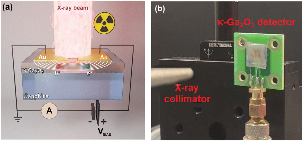 | ||
| Fig. 1 (a) Operating scheme of the fabricated κ-Ga2O3 photoconductive X-ray detector; (b) picture of the device mounted on a PCB board and positioned right in front of the X-ray collimator output slit. | ||
Prior to the deposition of the metal contacts, aimed at removing particulates and organic contaminants, the sample was cleaned in an ultrasonic bath in hot acetone for 5 min, then dipped in isopropanol for further 5 min, rinsed in deionized water, and finally dried in a pure N2 flow. Then, metal contacts were fabricated in a single step by RF magnetron sputtering deposition of a 300 nm thick Au film. The contact geometry (two rectangular 4.2 × 1.6 mm2 pads separated by a 1.0 mm-wide gap) was directly defined during deposition by the use of a stainless steel shadow mask positioned on the sample surface, with no need for photolithographic steps. The background pressure was 10−6 mbar, the target-to-substrate distance was 70 mm, and Ar was used as a sputter gas at a pressure of 2.5 × 10⁻² mbar. Finally, the detector was mounted on a standard printed circuit board (PCB) equipped with a SMA connector for biasing and current signal collection (Fig. 1(b)).
Characterization techniques and instrumentation
X-ray photocurrent measurements, as well as current–voltage characterization under dark conditions, were performed in continuous mode by using a low-noise electrometer (Keithley 487), simultaneously used as a voltage source for biasing the detector and as an ammeter. X-rays were produced by a standard Coolidge tube equipped with a Cu target (Kα line at 8.05 keV, Kβ line at 8.91 keV). The detector was centered in front of the X-ray tube collimator output slit (Fig. 1(b)), resulting in a 10 mm diameter circular spot-size (checked with a fluorescent screen) irradiating the whole active area of the detector. Au contacts being only 300 nm-thick, they are not able to perturb the response of the underlying κ-Ga2O3 film to X-rays, therefore the active area of the detector was considered to be a 4.2 × 4.2 mm2 square (i.e., the area where the applied electric field operates, below and between the contact pads). The X-ray tube accelerating voltage was fixed and set to be 40 kV. Conversely, the tube current was varied in the range of 2.5–40 mA, corresponding to a delivered dose rate in the range DR = 10–200 μGy s−1, as recorded in a reference ionization chamber (Farmer mod. NE 2536/3C) connected to a commercial dosimeter (Farmer mod. NE 2670).Spectral UV-Vis-NIR photoconductivity analysis in the 200–1000 nm range, used to investigate the role of defect states in photoconduction mechanisms, was performed by measuring the photocurrent generated by a monochromatic radiation focused on the 1 mm-wide gap between the two Au contact pads. Light came out from the output slit of a Newport Cornerstone 260 monochromator coupled to a Hg–Xe lamp. Aimed at reaching a higher sensitivity under sub-bandgap radiation, modulated measurements were performed. For this purpose, light was chopped at a frequency of 14 Hz by a SR540 chopper, and photogenerated current signals were converted using a low-noise transimpedance amplifier (Princeton Applied Research 181) into a voltage measured using a lock-in amplifier (EG&G 5209). Bias voltage was applied by means of a Keithley 487 electrometer, used as a voltage source only.
Results and discussion
Dark current measurements
Before irradiation under X-rays, the photoconductive detector was characterized under dark conditions to quantify the background noise level (i.e., the dark current) at different applied bias voltages, as well as to investigate on the presence of possible non-linear charge transport mechanisms (e.g., space charge limited current,37 or Frenkel–Poole emission38), which are well-known to negatively affect the performance of detectors based on the direct conversion of X-rays into electric charge.Fig. 2 reports the measured dark current Id values as a function of the bias voltage VBIAS, ranging from 0.1 to 500 V (corresponding approximately, by considering a 1 mm-wide interelectrode gap, to an applied electric field F varying in the range of 10−4–0.5 V μm−1). As can be seen from Fig. 2(a) (linear plot), Au contacts show excellent linearity in the full range of applied bias voltage, with the absence of undesirable non-linear effects triggered at high VBIAS values. Moreover, as can be inferred from Fig. 2(b) (log–log plot), linearity with the bias voltage extends for more than three decades, pointing out the ohmic behaviour of Au metal contacts on undoped κ-Ga2O3, differently from what was recently reported on n-type ε-Ga2O3, on which a Schottky junction was formed.39 We have to indeed consider the very high resistivity of undoped κ-Ga2O3: this implies that Fermi energy is located deep into the bandgap, and that the material is fully depleted in practice, leading to negligible band-bending at the metal–semiconductor interface, i.e., to the formation of an ohmic contact. It is also worth mentioning here that both ohmic and Schottky contacts demonstrated to be effective for κ-Ga2O3-based MSM detectors:40 in particular, ohmic contacts should be preferred to enhance the device responsivity, whereas Schottky contacts are better when the response speed is a key concern. In our case, Au ohmic contacts ensure extremely low dark current values, ranging from a few fA for VBIAS < 1 V (Fig. 2(b)) to a maximum value of 6.7 pA at VBIAS = 500 V (Fig. 2(a)), which confirms the very high resistivity ρd of the deposited epitaxial κ-Ga2O3 thin film. From the evaluation of the slope of the linear best-fit shown in Fig. 2(b), it is possible to obtain ρd = 3.15 × 10¹⁰ Ω cm, which exceeds by more than one order of magnitude the threshold requirement for semiconductor-based X-ray detectors (108–109 Ω cm).41
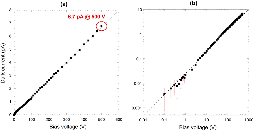 | ||
| Fig. 2 Linear (a) and log–log (b) plots showing the current–voltage curves of the fabricated X-ray detector measured under dark conditions. Dashed line represents in both cases the best linear fit to the experimental data. | ||
X-ray photoresponse evaluation
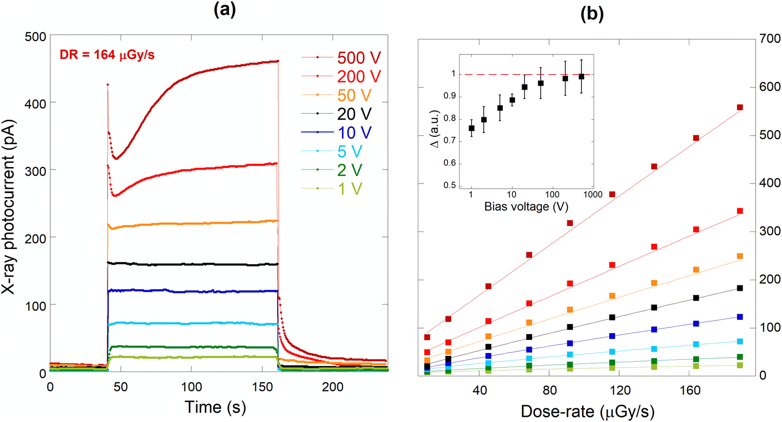
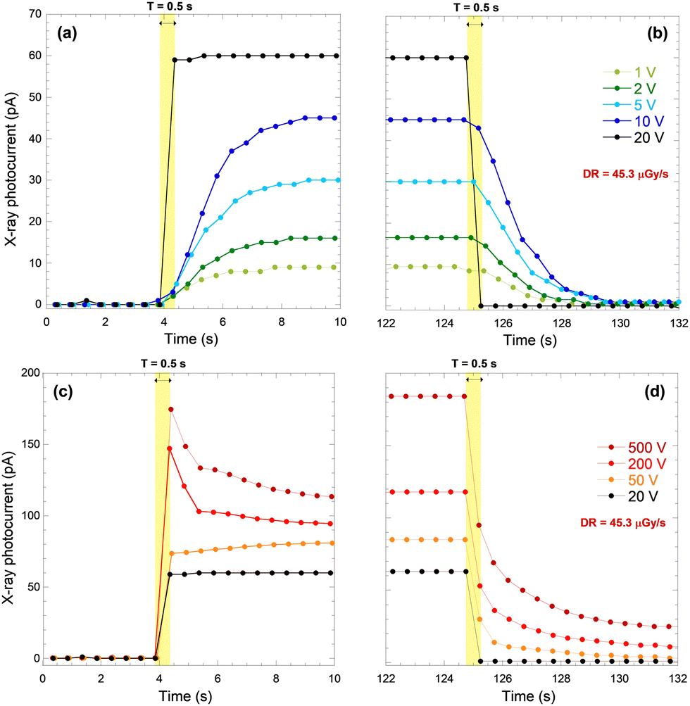
Transient photocurrent measurements under irradiation were performed at different bias voltages (in the range VBIAS = 1–500 V) and dose rates (approximately in the range DR = 10–200 μGy s−1) to evaluate within a single measurement session the main figures of merit of an X-ray detector: linearity with dose rate, sensitivity, response speed, and stability with time.Fig. 3 shows the time-dependent net photocurrents measured under X-ray on/off cycles (duty cycle 50%, time period 240 s) at low (1–20 V, Fig. 3(a)) and high (20–500 V, Fig. 3(b)) bias voltages, by progressively decreasing the dose rate at each “X-ray on” period. The net photocurrent Iph is given by Iph = Itot − Id, where Itot is the total current measured under irradiation. As expected, we can observe that: (1) at a given applied bias voltage, Iph increases with increasing dose rate; (2) at a given dose rate, Iph increases with increasing bias voltage. It is particularly worth noting the presence of a detectable signal even at VBIAS = 1 V, which corresponds to an applied electric field of only 10−3 V μm−1. Interestingly, the shape of the pulses is considerably different in the two operating regimes, as can be better appreciated in Fig. 4(a), showing a zoomed image of all the X-ray photocurrent pulses recorded in the bias voltage range of 1–500 V at the exemplary dose rate DR = 164 μGy s−1. It can be seen that at low bias voltages (1–20 V) the photocurrent fairly retraces the X-ray pulse excitation: the signal rapidly rises when the X-ray tube is switched on, then immediately settles down to its stationary value, and finally falls quickly to zero when the tube is switched off. Conversely, at high bias voltages (VBIAS > 20 V), after an initial overshoot followed by a rather fast decay, the signal increases very slowly towards its stationary value, which, however, is not even reached at the end of the “X-ray on” period (120 s); finally, an exponentially decaying residual signal is present after the tube is switched off.
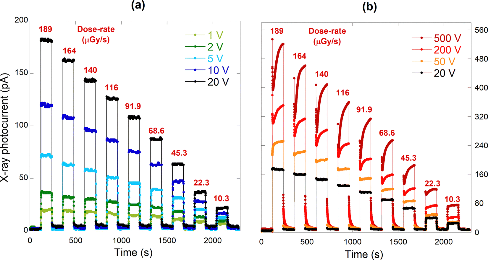 | ||
| Fig. 3 Time-dependent photocurrent of the fabricated photoconductive detector measured under X-ray on–off cycles at low (a) and high (b) bias voltages. The time period of a single on–off cycle was set to 240 s, with a 50% duty cycle. Dose rate progressively decreased from 189 to 10.3 μGy s−1 at each “X-ray on” period by decreasing the X-ray tube current from 40 to 2.5 mA (at a fixed tube acceleration voltage of 40 kV). | ||
 | ||
| Fig. 4 (a) Photocurrent signals recorded during a single “X-ray on” period (120 s) at different bias voltages; (b) stationary values of X-ray photocurrent as a function of the delivered dose rate at different bias voltages. Continuous lines represent the best power fit to the experimental data according to the Fowler's model (Iph ∝ DRΔ). The plot shown in the inset reports the estimated values of Fowler's linearity coefficient (Δ) for the different bias voltages. | ||
By considering the stationary X-ray net photocurrent values (extrapolated in the case VBIAS > 20 V) obtained from Fig. 3 at the different applied bias voltages, it is possible to analyze the behavior of the induced signal with the delivered dose rate (Fig. 4(b)). As can be seen, the device exhibits a fairly linear photoresponse with dose rate. The dependence perfectly follows the Fowler's model42 for electrical conductivity of solid-state detectors, according to which Iph ∝ DRΔ, where Δ is the linearity coefficient. Values of Δ around unity are always desirable, even mandatory in the case of applications where linearity with the delivered dose rate is essential, such as dosimetry for radiotherapy. In the case of the device investigated in this work, Δ increases with increasing bias voltage in the range Δ = 0.76–0.99 (see inset of Fig. 4(b)). It is known from the literature on ionizing radiation detectors based on wide-bandgap semiconductors43 that the value of Δ is strongly influenced by the presence of defects, the role of which in the dynamics of X-ray photogenerated charge transport is in turn significantly dependent on the intensity of the applied electric field. Indeed, when defects cause trapping of the photogenerated carriers, charge collection efficiency unavoidably decreases, unless the applied electric field is intense enough to induce detrapping, thus compensating for the temporary signal loss. This is most probably what happens in the case of κ-Ga2O3. At low fields, charge trapping results in a slightly sub-linear photoresponse with dose rate (Δ = 0.76–0.88 in the 1–10 V range), but linearity progressively improves at higher fields (Δ = 0.94–0.99 in the 20–500 V range), approaching the ideal value Δ = 1.
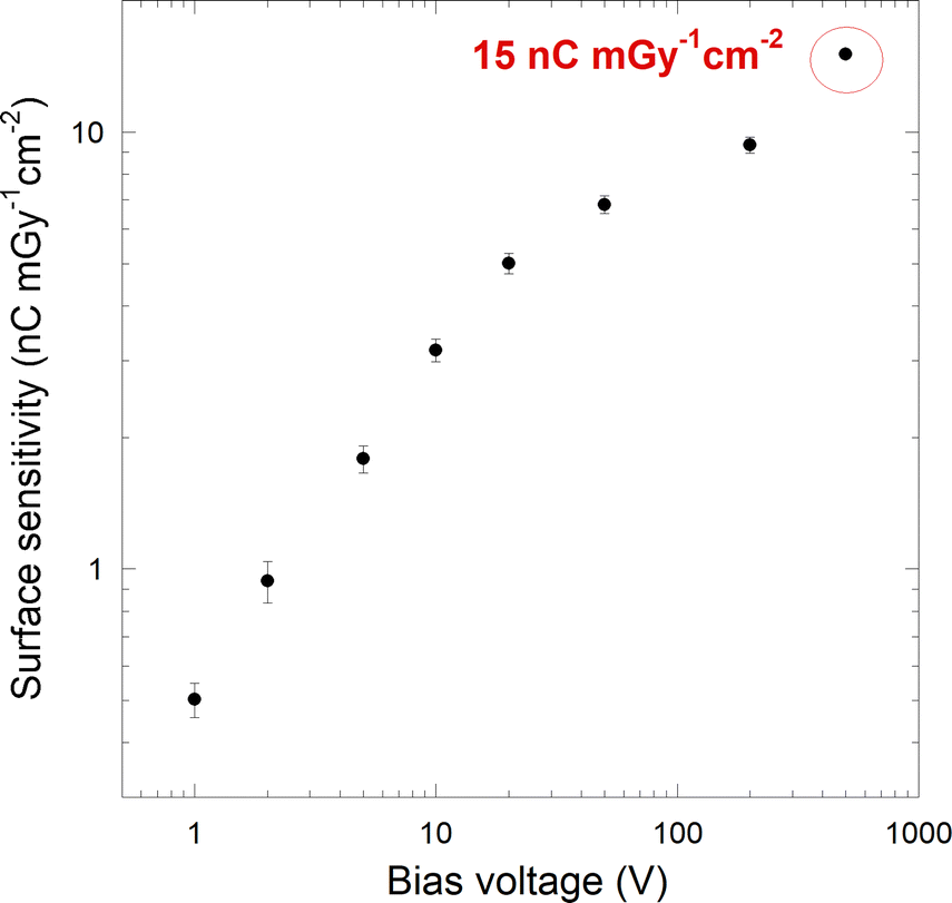
The fairly linear relationship between Iph and DR allowed us to estimate the surface specific sensitivity of the device, defined as S = Iph/(A·DR), where A = 4.2 × 4.2 mm2 is the active area of the detector. The estimation was performed by fitting the photocurrent data reported in Fig. 4(b) with linear curves (not shown), and then evaluating the different slopes as a function of the bias voltage. Fig. 5 reports the values obtained for S, ranging from 0.50 ± 0.04 nC mGy−1 cm−2 at VBIAS = 1 V to 15.06 ± 0.27 nC mGy−1 cm−2 at VBIAS = 500 V. Note that the relative uncertainty decreases with increasing bias voltage, owing to the better linearity of the photoresponse. If we consider the film thickness (440 nm), the normalized sensitivity to the active volume of the detector ranges from 11.42 ± 1.02 μC mGy−1 cm−3 at VBIAS = 1 V to 342.29 ± 6.24 μC mGy−1 cm−3 at VBIAS = 500 V; it is worth stressing here that the latter is an unprecedented value for Ga2O3-based X-ray detectors.28–32 Responsivity, defined as R = Iph/DR, ranges from 0.09 ± 0.01 μC Gy−1 at VBIAS = 1 V to 2.66 ± 0.05 μC Gy−1 at VBIAS = 500 V, and is comparable to values reported in the literature for bulk single-crystal β-Ga2O3.31,32
 | ||
| Fig. 5 Surface specific sensitivity of the fabricated X-ray κ-Ga2O3 detector as a function of the bias voltage. Error bars are related to the linear fitting of the experimental data shown in Fig. 4(b). | ||
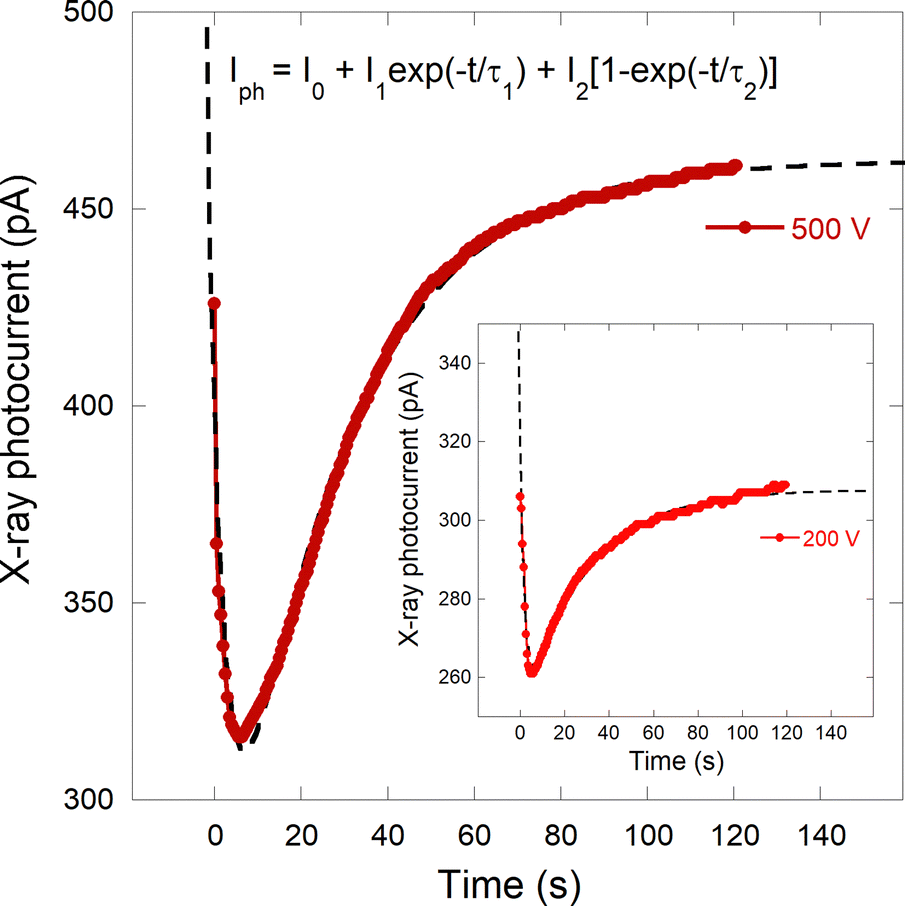
Unfortunately, the price to pay for a better linearity with dose rate and specific sensitivity at higher electric fields (in addition to the application of a high bias voltage, which is not desirable in any case) is a significantly longer time for the detector to reach a steady-state condition under irradiation, as it clearly appears from the 200 V and 500 V curves of Fig. 3(b) and 4(a). As can be seen, at high VBIAS, a photocurrent overshoot is triggered immediately after the irradiation starts, the amplitude of which increases with both increasing dose rate and bias voltage, i.e., both when a large amount of charge carriers is photogenerated (at higher DR) and is effectively collected by the electrodes (at higher VBIAS).
Photocurrent overshoots at the beginning of X-ray irradiation have already been observed in β-Ga2O3-based detectors,29 but no possible explanation was provided. However, transient photocurrent peaks appearing in a wide range of photoconductive devices, from diamond-based X-ray detectors44 to organic solar cells45 and light-emitting diodes,46 have been explained in the literature by trap-mediated space-charge effects. This is most likely what happens also in the case of κ-Ga2O3 at high bias voltages. At the beginning of the “X-ray on” period, the very fast rise of the photocurrent is due to the large amount of collected photogenerated carriers; however, we suppose that part of them gets trapped beneath the electrodes, causing space charge formation. As a consequence, an internal polarization electric field builds-up opposing the external bias, so that the charge collection efficiency is reduced, making the photocurrent decrease after peaking. A steady-state photocurrent should be reached at the end of the overshoot, soon after an equilibrium is established when polarization settles, but in our case the overshoot is followed by a very slow increase of the photocurrent, eventually exceeding (at the end of the “X-ray on” period) the overshoot peak value. This behavior may be explained by supposing that charge detrapping is triggered in the high-bias regime. To support this hypothesis, it is worth noting that the increase of photocurrent after the overshoot is more pronounced at higher bias voltages and higher dose rates, i.e., when the electric field is strong enough to promote charge detrapping and at the same time the radiation intensity is high enough to induce a significant trap-refilling.
A quantitative analysis of the timescales of the peak decay and the slow increase of photocurrent after the overshoot was performed, aimed at shedding light on the involved mechanisms. Two values of bias voltages were considered, namely, 200 V and 500 V. Curve fitting to the experimental data was performed by using the sum of two exponential functions, in the following form:
 | (1) |
 | ||
| Fig. 6 Curve fitting to experimental data of X-ray photocurrent at VBIAS = 500 V and (inset) VBIAS = 200 V. Dashed lines represent the best fit curves obtained by using eqn (1). For the sake of simplicity, the overshoot peaking time was assumed to be t = 0. | ||
The obtained values, averaged over all the dose rates in the range of 22.3–189 μGy s−1 (where the overshoot is present), are τ1 = 2.13 ± 0.07 s and τ2 = 32.48 ± 0.57 s for 200 V, and τ1 = 3.57 ± 0.09 s and τ2 = 31.82 ± 0.41 s for 500 V. Such values are consistent with the time constants of charge trapping/detrapping mechanisms reported for both β-Ga2O3- and κ-Ga2O3-based MSM photodetectors for UV radiation.47,48 It is worth recalling here that trapping/detrapping time constants are governed by the energy depth of the traps,48 and that longer time constants are related to deeper traps. As can be inferred from our results, the timescale (few seconds) of the peak decay (τ1) is consistent with charge trapping by shallow defects, responsible for the space charge formation after peaking, whereas the very high values (few tens of seconds) of τ2 justify a predominant detrapping from deep levels in the second stage of the transient regime. Once trapping and detrapping rates are equal, and a constant electric field is established between the collecting electrodes as well, a steady-state photocurrent is eventually reached.
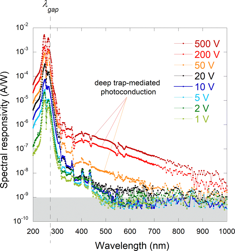
To further support our hypotheses on the role of sub-bandgap defects on charge transport, spectral photoconductivity measurements were performed in the 200–1000 nm range. Fig. 7 reports the spectral responsivity SR of the κ-Ga2O3 epitaxial thin film measured at the same bias voltages (1–500 V) used for the X-ray characterization session; SR was calculated as a function of the impinging wavelength λ as SR(λ) = |Iph(λ)|/P(λ), where |Iph| is the modulus of the measured modulated photocurrent, and P is the power of the monochromatic radiation focused on the active area of the device. As expected, responsivity increases with increasing bias voltage, denoting a progressively better charge collection efficiency. In addition, all spectra show the presence of shallow traps, appearing as band-tails for λgap < λ < 320 nm, where λgap ≈ 270 nm is the wavelength corresponding to the energy bandgap (≈4.6 eV). More interestingly, note that photoconduction mediated by deep traps (λ > 320 nm) is boosted in the high-bias regime, increasing considerably at VBIAS = 50, 200, and 500 V; this experimentally confirms our hypothesis on detrapping from deep levels as the predominant photoconduction mechanism acting in the second stage of the X-ray photocurrent transient regime.
 | ||
| Fig. 7 Spectral responsivity of the κ-Ga2O3 epitaxial thin film in the 200–1000 nm range at different bias voltages. Dashed line indicates the wavelength λgap ≈ 270 nm corresponding to the energy bandgap (≈4.6 eV). Measurement points within the grey band have to be considered below the background noise level. | ||
In addition to sensitivity and linearity with the dose rate, another valuable figure of merit for X-ray detectors is the response speed. By taking a closer look at the shape of a photocurrent pulse recorded during a single “X-ray on” period (Fig. 8), it is possible to evaluate the response speed of the κ-Ga2O3 film in terms of rise time tr (defined as the time required for the pulse to rise from 10% to 90% of its peak value) and decay time td (defined as the time required for the pulse to decay from 90% to 10% of its peak value). At low bias voltages (1–10 V), tr and td are approximately equal, and vary in the range of 1–2 s; in particular, both tr and td decrease slightly with increasing applied electric field (see Fig. 8(a) and (b)). Both the measured values (in the range of a few seconds) and the dependence on the bias voltage are in agreement with the typical electron/hole trapping effect, already reported in the literature for β-Ga2O3.49 A higher bias voltage leads indeed to a faster charge collection and reduces the charge trapping probability, decreasing both the rise and the decay time; in this sense, narrowing the electrode spacing (by using interdigitated contacts, for example) may be surely helpful for speeding up the photoresponse in the low-bias regime. When VBIAS = 20 V, tr and td are both lower than 0.5 s; however, it is worth stressing here that this value should be considered as an upper limit for our device, because it represents the minimum delay time between two consecutive measurement points obtainable with the electrometer used for the experiments. Indeed, as recently reported on X-ray detectors based on ε-Ga2O3 epitaxial thin films grown by MOCVD,50,51 and tested with a faster front-end electronics, the actual rise and decay times may be significantly lower (<50 ms).
 | ||
| Fig. 8 Rising (a)–(c) and decaying (b)–(d) dynamics of photocurrent pulses recorded during a single “X-ray on” period (120 s) at low (a), (b) and high (c), (d) bias voltages. Dose rate was set to 45.3 μGy s−1, but similar results have been obtained at all other investigated dose rate values. | ||
As can be inferred from Fig. 8, the biasing condition VBIAS = 20 V ensures the best performance in terms of response speed and recovery time; the signal reaches its stationary value soon after X-ray irradiation starts, then immediately falls to zero when X-ray is shut down. At higher bias voltages (VBIAS > 20 V), pulse rising and decaying dynamics gets progressively slower (see Fig. 8(c) and (d)). In this operating regime, the applied bias is indeed high enough to trigger both space charge formation and detrapping, thus requiring longer times to obtain a stable photocurrent when X-rays are on, as well as to recover the initial conditions at the end of the irradiation period. We can therefore deduce that VBIAS = 20 V represents an optimal operating condition for the fabricated device, ensuring at the same time a fast response (tr, td < 0.5 s) and a very good specific sensitivity (S = 5 nC mGy−1 cm−2) to X-rays; most probably, the corresponding applied electric field is in this case high enough to ensure a fast and efficient charge collection, and at the same time low enough to avoid both photocurrent “crowding” beneath the electrodes (thus hampering space charge formation) and detrapping from deep levels.
Operation of the device at the optimal bias voltage (20 V) was then used to verify the signal reproducibility at a given dose rate, as well as to preliminarily assess the detector's response stability with time. Fig. 9 reports the X-ray photocurrent signal recorded at VBIAS = 20 V in a 2 h measurement session at the highest investigated dose rate (189 μGy s−1). In the first part of the session, the device was tested with 10 X-ray on–off cycles (duty cycle 50%, time period 360 s), and the recorded signal pulses demonstrated an excellent reproducibility. Then, the device was kept for 60 min under the maximum X-ray flux, producing a perfectly stable signal, only varying within ±1.5% of its average stationary value (165.5 pA, see Fig. 9).
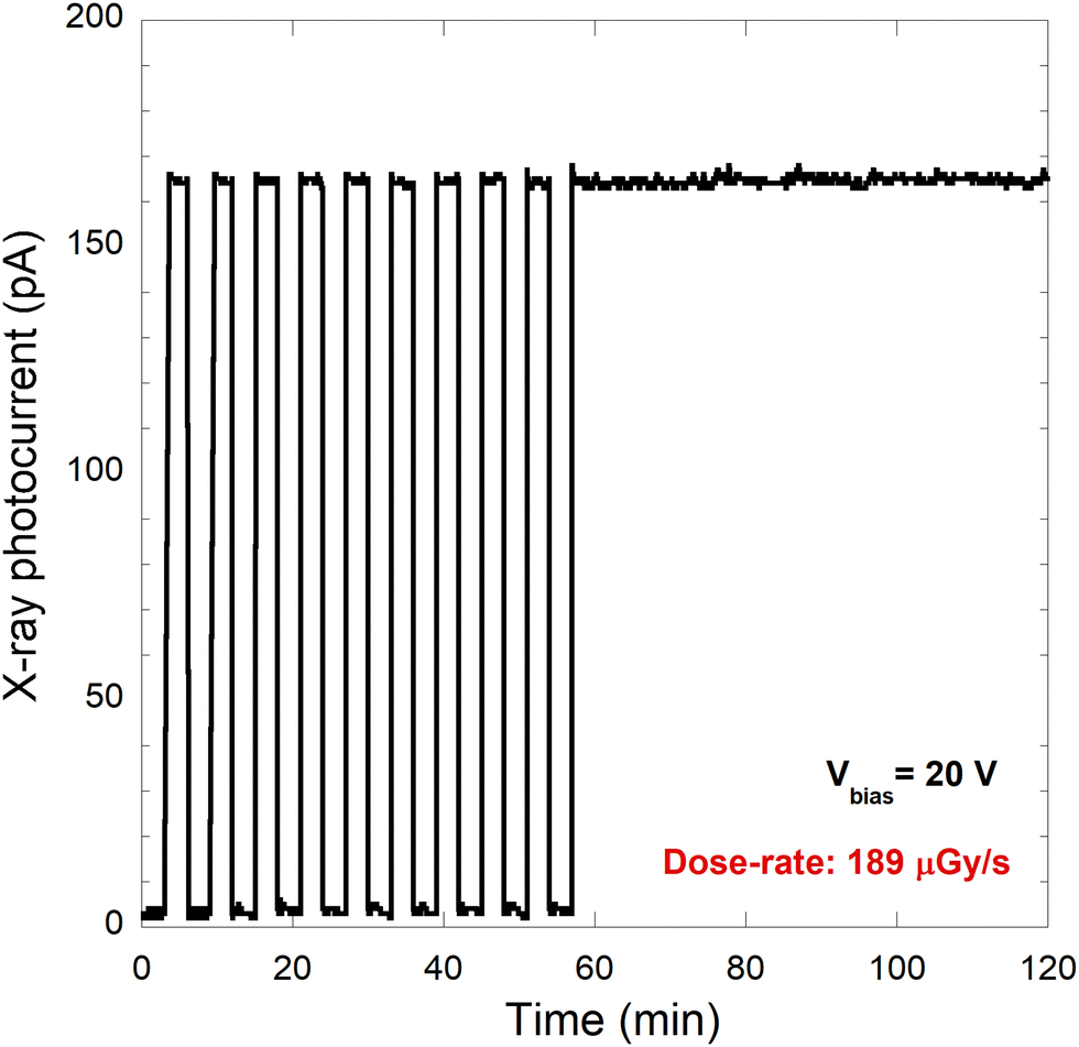 | ||
| Fig. 9 X-ray photocurrent recorded with the fabricated κ-Ga2O3-based detector in a measurement session consisting of two parts: (1) 10 on–off cycles (6 min each); (2) 1 h of continuous irradiation. Bias voltage and dose rate were set to 20 V and 189 μGy s−1, respectively. | ||
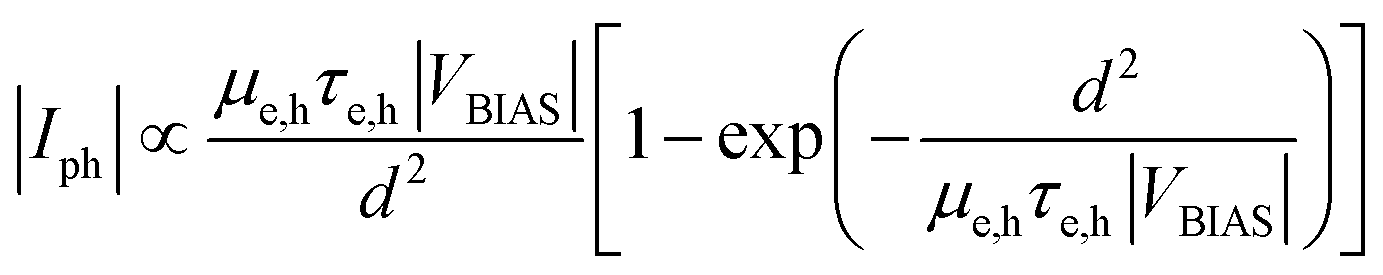
X-ray irradiation was finally profitably used to evaluate the average mobility-lifetime product μe,hτe,h of the photogenerated carriers, which is the most significant figure of merit for the charge transport properties of a semiconductor, being directly related to the concentration of defects acting as recombination centers for both electrons and holes. (i.e., it provides an estimate of the crystalline quality of the deposited film). A simple way to extract the μe,hτe,h product is by fitting the X-ray photocurrent Iphvs. VBIAS curve according to Hecht's equation:52
 | (2) |
Fig. 10(a) reports the experimental results obtained by irradiating the fabricated detector at different dose rates. Best fits returned μe,hτe,h = (1.91 ± 0.07) × 10−4 cm2 V−1 at DR = 189 μGy s−1, μe,hτe,h = (2.37 ± 0.08) × 10−4 cm2 V−1 at DR = 91.9 μGy s−1, and μe,hτe,h = (3.13 ± 0.12) × 10−4 cm2 V−1 at DR = 45.3 μGy s−1. The first result to be noted is that all the estimated μe,hτe,h values are about one order of magnitude higher than those recently reported for single-crystal Fe-doped β-Ga2O3-based detectors tested under the same experimental conditions (type of X-ray source, accelerating voltage, and tube current).26 This is most probably due to a higher lifetime of the photogenerated carriers before recombination; indeed, high Fe-doping of β-Ga2O3, necessary to increase the material resistivity and lower the dark current, greatly reduces both the carrier drift length and the carrier collection efficiency, due to the introduction of deep-level impurities.53 Moreover, it is worth noting from Fig. 10(a) that μe,hτe,h decreases slightly with an increasing dose rate, presumably due to a higher density of photogenerated charge, enhancing carrier–carrier scattering effects which can limit carrier mobility.
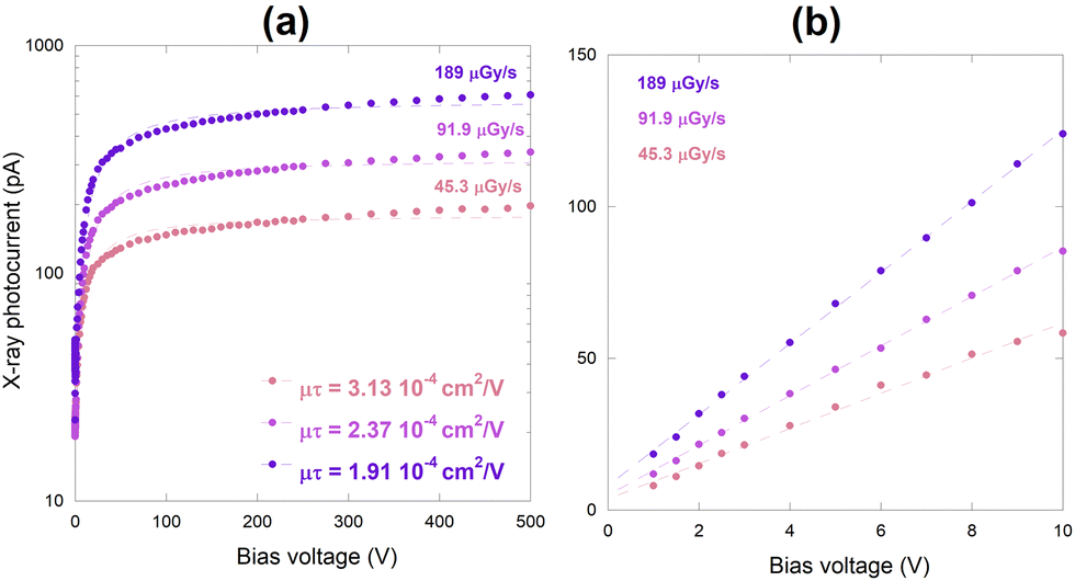 | ||
| Fig. 10 (a) Experimental results for the evaluation of the average mobility-lifetime product at different dose rates. Bias voltage was varied in the 1–500 V range. In all the cases, dashed lines show the best fit to data obtained by using Hecht's eqn (2); (b) the same plot as Fig. 10(a) zoomed in the 1–10 V range, aimed at showing the ohmic behaviour of the metal contact under X-ray irradiation. Dashed lines represent the best linear fit to experimental data. | ||
It is also interesting to observe that the ohmicity of the metal contact remains even under X-ray irradiation, as can be inferred from Fig. 10(b), showing a zoomed image (in the 1–10 V range) of the plot reported in Fig. 10(a). In this regime of applied bias voltages, in which the photocurrent saturation is not started yet, the exponential term of Hecht's equation can be indeed neglected to a first approximation, and the relationship between Iph and VBIAS is linearized. In this way, the contact ohmicity can be correctly verified, as in our case. Moreover, it can be inferred from Fig. 10(b) that the slope of the linear fitting curve increases with increasing dose rate, as expected from a photoconductive device, the conductivity of which is directly proportional to the intensity of the absorbed radiation.
Conclusions
Epitaxial orthorhombic κ-Ga2O3 was tested for the first time under X-rays to assess its suitability as an active material for the development of photoconductive direct X-ray detectors. The results showed that κ-Ga2O3 offers an optimal combination of properties useful for the development of sensitive, fast, and stable X-ray detectors with minimum power consumption. This can be inferred from Table 1, comparing the main X-ray photoresponse properties of κ-Ga2O3 obtained in this work to those of other Ga2O3-based active materials recently reported in the literature.It is worth highlighting that κ-Ga2O3 shows the highest normalized sensitivity to the active volume, and is the only polymorph which demonstrates excellent stability under 120 min of X-ray irradiation, without showing any degradation of the photoresponse. It shares with amorphous (a-) Ga2O3 and nanocrystalline (nc-) β-Ga2O3 the advantage, if compared to β-Ga2O3 single crystals, of being deposited as a thin film, allowing for the fabrication of large-area devices. It is slightly slower than nc-β-Ga2O3, but significantly faster than a-Ga2O3, and more responsive than both in a wider operating voltage range. Fe-doped single-crystal (sc-) β-Ga2O3 shows better properties than κ-Ga2O3 in terms of rise time and responsivity, but at the expense of very high bias voltage, which makes it unsuitable, for instance, for the implementation of low-power portable devices; conversely, undoped sc-β-Ga2O3 can operate at low bias voltages, but it shows both a slower response and a lower responsivity than κ-Ga2O3.
In conclusion, in comparison with the other members of the gallium oxide family, κ-Ga2O3 demonstrated to be the most versatile candidate for the fabrication of direct X-ray detectors, the performance of which can be tailored to the specific user's requirements, depending on the operating voltage. High bias regimes (VBIAS > 20 V) are to be preferred to maximize sensitivity and linearity with X-ray dose rate regardless of the response speed, but low bias operation (down to 1 V) is also possible, with the advantage of a very low power consumption. In this work, it is shown that an intermediate bias voltage (VBIAS = 20 V) is the optimal solution, ensuring the best trade-off between sensitivity and linearity with the dose rate, as well as a fast and rapidly stable photoresponse. Anyway, it is finally worth mentioning that, by reducing the gap between the electrodes at values lower than 1 mm (e.g., by the use of interdigitated electrodes fabricated by photolithographic techniques), it is possible to further reduce the value of the applied bias voltage while maintaining the same charge collection performance.
Conflicts of interest
There are no conflicts to declare.Acknowledgements
The authors would like to thank Antonello Ranieri (IC-CNR, Istituto di Cristallografia, Consiglio Nazionale delle Ricerche) for the valuable technical support, Antonella Parisini, Maura Pavesi, Alessio Bosio, and Francesco Mezzadri (Università di Parma) for useful discussion and preliminary evaluation of the κ-Ga2O3 epitaxial films used in this work.References
- J. M. Dos Santos and C. M. Monteiro, The response of high-purity germanium detectors to X-rays with energy in the region of the Ge K-absorption edge, Appl. Radiat. Isot., 2001, 55, 331 CrossRef CAS PubMed.
- G. Conte, M. Girolami, S. Salvatori and V. Ralchenko, X-ray diamond detectors with energy resolution, Appl. Phys. Lett., 2007, 91, 183515 CrossRef.
- M. Girolami, P. Allegrini, G. Conte, D. M. Trucchi and V. G. Ralchenko, Diamond Detectors for UV and X-Ray Source Imaging, IEEE Electron Device Lett., 2012, 33, 224 CAS.
- L. Abbene, F. Principato, G. Gerardi, A. Buttacavoli, D. Cascio, M. Bettelli, N. S. Amadè, P. Seller, M. C. Veale, O. Fox, K. Sawhney, S. Zanettini, E. Tomarchio and A. Zappettini, Room-temperature X-ray response of cadmium–zinc–telluride pixel detectors grown by the vertical Bridgman technique, J. Synchrotron Radiat., 2020, 27, 319 CrossRef CAS PubMed.
- I. Temiño, L. Basiricò, I. Fratelli, A. Tamayo, A. Ciavatti, M. Mas-Torrent and B. Fraboni, Morphology and mobility as tools to control and unprecedentedly enhance X-ray sensitivity in organic thin-films, Nat. Commun., 2020, 11, 2136 CrossRef PubMed.
- J. Liu, B. Shabbir, C. Wang, T. Wan, Q. Ou, P. Yu, A. Tadich, X. Jiao, D. Chu, D. Qi, D. Li, R. Kan, Y. Huang, Y. Dong, J. Jasieniak, Y. Zhang and Q. Bao, Flexible, Printable Soft-X-Ray Detectors Based on All-Inorganic Perovskite Quantum Dots, Adv. Mater., 2019, 31, 1901644 CrossRef PubMed.
- A. Ciavatti, T. Cramer, M. Carroli, L. Basiricò, R. Fuhrer, D. M. De Leeuw and B. Fraboni, Dynamics of direct X-ray detection processes in high-Z Bi2O3 nanoparticles-loaded PFO polymer-based diodes, Appl. Phys. Lett., 2017, 111, 183301 CrossRef.
- K. Motoki, Y. Miyazawa, D. Kobayashi, M. Ikegami, T. Miyasaka, T. Yamamoto and K. Hirose, Degradation of CH3NH3PbI3 perovskite due to soft X-ray irradiation as analyzed by an X-ray photoelectron spectroscopy time-dependent measurement method, J. Appl. Phys., 2017, 121, 085501 CrossRef.
- G. Kakavelakis, M. Gedda, A. Panagiotopoulos, E. Kymakis, T. D. Anthopoulos and K. Petridis, Metal Halide Perovskites for High-Energy Radiation Detection, Adv. Sci., 2020, 7, 2002098 CrossRef CAS PubMed.
- T.-T. Kuo, C.-M. Wu, H.-H. Lu, I. Chan, K. Wang and K.-C. Leou, Flexible X-ray imaging detector based on direct conversion in amorphous selenium, J. Vac. Sci. Technol., A, 2014, 32, 041507 CrossRef.
- K. Hellier, E. Benard, C. C. Scott, K. S. Karim and S. Abbaszadeh, Recent Progress in the Development of a-Se/CMOS Sensors for X-ray Detection, Quantum Beam Sci., 2021, 5, 29 CrossRef CAS.
- J. Chen, H. Tang, Z. Li, Z. Zhu, M. Gu, J. Xu, X. Ouyang and B. Liu, Highly sensitive X-ray detector based on a β-Ga2O3:Fe single crystal, Opt. Express, 2021, 29, 23292 CrossRef CAS PubMed.
- J. Kim, S. J. Pearton, C. Fares, J. Yang, F. Ren, S. Kima and A. Y. Polyakov, Radiation damage effects in Ga2O3 materials and devices, J. Mater. Chem. C, 2019, 7, 10 RSC.
- F. Boschi, M. Bosi, T. Berzina, E. Buffagni, C. Ferrari and R. Fornari, Hetero-epitaxy of κ-Ga2O3 layers by MOCVD and ALD, J. Cryst. Growth, 2016, 443, 25 CrossRef CAS.
- A. Kuramata, K. Koshi, S. Watanabe, Y. Yamaoka, T. Masui and S. Yamakoshi, High-quality β-Ga2O3 single crystals grown by edge-defined film-fed growth, Jpn. J. Appl. Phys., 2016, 55, 1202A2 CrossRef.
- Z. Galazka, R. Uecker, D. Klimm, K. Irmscher, M. Naumann, M. Pietsch, A. Kwasniewski, R. Bertram, S. Ganschow and M. Bickermann, Scaling-up of bulk β-Ga2O3 single crystals by the Czochralski method, ECS J. Solid State Sci. Technol., 2017, 6, Q3007 CrossRef CAS.
- S. J. Pearton, J. Yang, P. H. Cary IV, F. Ren, J. Kim, M. J. Tadjer and M. A. Mastro, A review of Ga2O3 materials, processing, and devices, Appl. Phys. Rev., 2018, 5, 011301 Search PubMed.
- K. Kaneko, S. Fujita and T. Hirtora, A power device material of corundum-structured α-Ga2O3 fabricated by MIST EPITAXY® technique, Jpn. J. Appl. Phys., 2018, 57, 02CB18 CrossRef.
- M. Pavesi, F. Fabbri, F. Boschi, G. Piacentini, A. Baraldi, M. Bosi, E. Gombia, A. Parisini and R. Fornari, κ-Ga2O3 epilayers as a material for solar-blind UV photodetectors, Mater. Chem. Phys., 2018, 205, 502 CrossRef CAS.
- I. Cora, F. Mezzadri, F. Boschi, M. Bosi, M. Caplovicova, G. Calestani, I. Dódony, B. Pécz and R. Fornari, Real structure of ε-Ga2O3 and its relation to κ phase, CrystEngComm, 2017, 19, 1509 RSC.
- M. Biswas and H. Nishinaka, Thermodynamically metastable α-, ε- (or κ-), and γ-Ga2O3: From material growth to device applications, APL Mater., 2022, 10, 060701 CrossRef CAS.
- P. Mazzolini, Z. Fogarassy, A. Parisini, F. Mezzadri, D. Diercks, M. Bosi, L. Seravalli, A. Sacchi, G. Spaggiari, D. Bersani, O. Bierwagen, B. M. Janzen, M. N. Marggraf, M. R. Wagner, I. Cora, B. Pécz, A. Tahraoui, A. Bosio, C. Borelli, S. Leone and R. Fornari, Silane-Mediated Expansion of Domains in Si-Doped κ-Ga2O3 Epitaxy and its Impact on the In-Plane Electronic Conduction, Adv. Funct. Mater., 2022, 33, 2207821 CrossRef.
- K. Jiang, J. Tang, M. J. Cabral, A. Park, L. Gu, R. F. Davis and L. M. Porter, Layered phase composition and microstructure of κ-Ga2O3-dominant heteroepitaxial films grown via MOCVD, J. Appl. Phys., 2022, 131, 055305 CrossRef CAS.
- E. Dobročka, F. Gucmann, K. Hušeková, P. Nádaždy, F. Hrubišák, F. Egyenes, A. Rosová and M. Mikolášek, M. Ťapajna, Structure and Thermal Stability of ε/κ-Ga2O3 Films Deposited by Liquid-Injection MOCVD, Materials, 2023, 16, 20 CrossRef.
- F. Mezzadri, G. Calestani, F. Boschi, D. Delmonte, M. Bosi and R. Fornari, Crystal Structure and Ferroelectric Properties of κ-Ga2O3 Films Grown on (0001)-Sapphire, Inorg. Chem., 2016, 55, 12079 CrossRef PubMed.
- S. Leone, R. Fornari, M. Bosi, V. Montedoro, L. Kirstea, P. Philipp Doering, F. Benkhelifa, M. Prescher, C. Manz, V. Polyakov and O. Ambacher, Epitaxial growth of GaN/Ga2O3 and Ga2O3/GaN heterostructures for novel high electron mobility transistors, J. Cryst. Growth, 2020, 534, 125511 CrossRef CAS.
- P. Ranga, S. B. Cho, R. Mishra and S. Krishnamoorthy, Highly tunable, polarization-engineered two-dimensional electron gas in ε-AlGaO3/ε-Ga2O3 heterostructures, Appl. Phys. Express, 2020, 13, 061009 CrossRef CAS.
- H. Liang, S. Cui, R. Su, P. Guan, Y. He, L. Yang, L. Chen, Y. Zhang, Z. Mei and X. Du, Flexible X-ray Detectors Based on Amorphous Ga2O3 Thin Films, ACS Photonics, 2019, 6, 351 CrossRef CAS.
- M. Chen, Z. Zhang, R. Zhan, J. She, S. Deng, N. Xu and J. Chen, Fast-response X-ray detector based on nanocrystalline Ga2O3 thin film prepared at room temperature, Appl. Surf. Sci., 2021, 554, 149619 CrossRef CAS.
- I. Hany, G. Yang and C.-C. Chung, Fast X-ray detectors based on bulk β-Ga2O3 (Fe), J. Mater. Sci., 2020, 55, 9461 CrossRef CAS.
- J. Chen, H. Tang, Z. Li, Z. Zhu, M. Gu, J. Xu, X. Ouyang and B. Liu, Highly sensitive X-ray detector based on a β-Ga2O3:Fe single crystal, Opt. Express, 2021, 29, 23292 CrossRef CAS PubMed.
- X. Lu, L. Zhou, L. Chen, X. Ouyang, H. Tang, B. Liu and J. Xu, X-ray Detection Performance of Vertical Schottky Photodiodes Based on a Bulk β-Ga2O3 Substrate Grown by an EFG Method, ECS J. Solid State Sci. Technol., 2019, 8, Q3046 CrossRef CAS.
- R. Fornari, M. Pavesi, V. Montedoro, D. Klimm, F. Mezzadri, I. Cora, B. Pécz, F. Boschi, A. Parisini, A. Baraldi, C. Ferrari, E. Gombia and M. Bosi, Thermal stability of κ-Ga2O3 polymorph, Acta Mater., 2017, 140, 41 CrossRef.
- I. Cora, Zs Fogarassy, R. Fornari, M. Bosi, A. Rečnik and B. Pécz, In situ TEM study of κ → β and κ → γ phase transformations in Ga2O3, Acta Mater., 2020, 183, 216 CrossRef CAS.
- M. Bosi, P. Mazzolini, L. Seravalli and R. Fornari, Ga2O3 polymorphs: Tailoring the epitaxial growth conditions, J. Mater. Chem. C, 2020, 8, 10975 RSC.
- M. Bosi, L. Seravalli, P. Mazzolini, F. Mezzadri and R. Fornari, Thermodynamic and Kinetic Effects on the Nucleation and Growth of κ/κ- or β-Ga2O3 by Metal–Organic Vapor Phase Epitaxy, Cryst. Growth Des., 2021, 21, 6393 CrossRef CAS.
- A. Bosio, C. Borelli, A. Parisini, M. Pavesi, S. Vantaggio, R. Fornari and A. Metal-Oxide, Contact to ε-Ga2O3 Epitaxial Films and Relevant Conduction Mechanism, ECS J. Solid State Sci. Technol., 2020, 9, 055002 CrossRef CAS.
- M. Girolami, A. Bellucci, P. Calvani, R. Flammini and D. M. Trucchi, Radiation-assisted Frenkel-Poole transport in single-crystal diamond, Appl. Phys. Lett., 2013, 103, 083502 CrossRef.
- Z. Liu, Y. Huang, C. Zhang, J. Wang, H. Li, Z. Wu, P. Li and W. Tang, Fabrication of ε-Ga2O3 solar-blind photodetector with symmetric interdigital Schottky contacts responding to low intensity light signal, J. Phys. D: Appl. Phys., 2020, 53, 295109 CrossRef CAS.
- M. Cui, Y. Xu, X. Sun, Z. Wang, H. Gong, X. Chen, T. Hu, Y. Zhang, F. Ren, S. Gu, J. Ye and R. Zhang, Photoconductive and photovoltaic metal–semiconductor–metal κ-Ga2O3 solar-blind detectors with high rejection ratios, J. Phys. D: Appl. Phys., 2022, 55, 394003 CrossRef.
- S. Wu, C. Liang, J. Zhang, Z. Wu, X.-L. Wang, R. Zhou, Y. Wang, S. Wang, D.-S. Li and T. Wu, A Photoconductive X-ray Detector with a High Figure of Merit Based on an Open-Framework Chalcogenide Semiconductor, Angew. Chem., Int. Ed., 2020, 59, 18605 CrossRef CAS PubMed.
- J. F. Fowler and F. H. Attix, in Solid state electrical conductivity dosimeters, ed. F. H. Attix and W. C. Roesch, Radiation Dosimetry, Academic Press, New York, 2nd edn, 1966, ch. 14 Search PubMed.
- N. Ade and T. L. Nam, The influence of defect levels on the dose rate dependence of synthetic diamond detectors of various types on exposures to high-energy radiotherapy beams, Rad. Phys. Chem., 2015, 108, 65 CrossRef CAS.
- P. Bergonzo, D. Tromson, C. Descamps, H. Hamrita, C. Mer, N. Tranchant and M. Nesladek, Improving diamond detectors: A device case, Diamond Relat. Mater., 2007, 16, 1038 CrossRef CAS.
- I. Hwang, C. R. McNeill and N. C. Greenham, Drift-diffusion modeling of photocurrent transients in bulk heterojunction solar cells, J. Appl. Phys., 2009, 106, 094506 CrossRef.
- M. Diethelm, M. Bauer, W.-H. Hu, C. Vael, S. Jenatsch, P. W. M. Blom, F. Nüesch and R. Hany, Electron Trap Dynamics in Polymer Light-Emitting Diodes, Adv. Funct. Mater., 2022, 32, 2106185 CrossRef CAS.
- Y. Cai, K. Zhang, Q. Feng, Y. Zuo, Z. Hu, Z. Feng, H. Zhou, X. Lu, C. Zhang, W. Tang, J. Zhang and Y. Hao, Tin-assisted growth of ε-Ga2O3 film and the fabrication of photodetectors on sapphire substrate by PLD, Opt. Mater. Express, 2018, 8, 3506 CrossRef CAS.
- D. Guo, Z. Wu, P. Li, Y. An, H. Liu, X. Guo, H. Yan, G. Wang, C. Sun, L. Li and W. Tang, Fabrication of β-Ga2O3 thin films and solar-blind photodetectors by laser MBE technology, Opt. Mater. Express, 2014, 4, 1067 CrossRef.
- D. Patil-Chaudhari, M. Ombaba, J. Y. Oh, H. Mao, K. H. Montgomery, A. Lange, S. Mahajan, J. M. Woodall and M. S. Islam, Solar Blind Photodetectors Enabled by Nanotextured β-Ga2O3 Films Grown via Oxidation of GaAs Substrates, IEEE Photonics J., 2017, 9, 2300207 Search PubMed.
- Z. Zhang, Z. Chen, M. Chen, K. Wang, H. Chen, S. Deng, G. Wang and J. Chen, ε-Ga2O3 Thin Film Avalanche Low-Energy X-Ray Detectors for Highly Sensitive Detection and Fast-Response Applications, Adv. Mater. Technol., 2021, 6, 2001094 CrossRef CAS.
- J. Wang, L. Zhou, X. Lu, L. Chen, Z. Chen, X. Zou, G. Wang, B. Yang and X. Ouyang, Pulsed X-Ray Detector Based on an Unintentionally-Doped High Resistivity ε-Ga2O3 Film, IEEE Photonics Technol. Lett., 2023, 35, 89 CAS.
- K. Hecht, Zum Mechanismus des lichtelektrischen Primärstromes in isolierenden Kristallen, Z. Phys., 1932, 77, 235 CrossRef CAS.
- Z. Li, J. Chen, H. Tang, Z. Zhu, M. Gu, J. Xu, L. Chen, X. Ouyang and B. Liu, ACS Appl. Electron. Mater., 2021, 3, 4630 CrossRef CAS.
Footnote |
| † Electronic supplementary information (ESI) available. See DOI: https://doi.org/10.1039/d2tc05297k |
| This journal is © The Royal Society of Chemistry 2023 |