
Crystallinity-modulated hollow CeO2−x nanorods as free radical scavengers for long-term photostability in organic photovoltaics†
Seongwon
Yoon‡
 a,
Taehyun
Kwon‡
bc,
Sohyun
Kim
b,
So Hyun
Park
ad,
Youngjoon
Lim
b,
Jihun
Kim
e,
Jun
Kim
b,
Kwangjin
An
e,
Sungmin
Park
f,
Jin Young
Kim
*b and
Hae Jung
Son
*ad
a,
Taehyun
Kwon‡
bc,
Sohyun
Kim
b,
So Hyun
Park
ad,
Youngjoon
Lim
b,
Jihun
Kim
e,
Jun
Kim
b,
Kwangjin
An
e,
Sungmin
Park
f,
Jin Young
Kim
*b and
Hae Jung
Son
*ad
aAdvanced Photovoltaics Research Center, Korea Institute of Science and Technology (KIST), Seoul 02792, Republic of Korea. E-mail: hjson@kist.re.kr
bHydrogen Fuel Cell Research Center, KIST, Seoul 02792, Republic of Korea. E-mail: jinykim@kist.re.kr
cDepartment of Chemistry and Research Institute of Basic Sciences, Incheon National University, Incheon 22012, Republic of Korea
dGraduate School of Energy and Environment (KU-KIST Green School), Korea University, Seoul 02841, Republic of Korea
eSchool of Energy and Chemical Engineering, Ulsan National Institute of Science and Technology (UNIST), Ulsan 44919, Republic of Korea
fRealistic Media Research Center, ICT Convergence Research Division, Gumi Electronics & Information Technology Research Institute (GERI), Gumi, Gyeongbuk 39253, Republic of Korea
First published on 19th December 2022
Abstract
Here we investigated the effects of CeO2−x nanostructures as free radical scavengers on the long-term photostability of an organic photovoltaic (OPV) structure. From powder X-ray diffraction, Raman spectroscopy, X-ray photoelectron spectroscopy, and N2 adsorption experiments, it was determined that the single-crystalline hollow CeO2−x nanorods were very effective as hydroxyl radical scavengers. This was attributed to their having more Ce3+ states and a wider surface area than other types of CeO2 nanostructures. Time-dependent UV-visible absorption spectra analyses also revealed that the improved scavenging of hydroxyl radicals in the OPV device was related to the better interfacial compatibility between the organic active and ZnO layers, resulting in improved OPV photostability.
1. Introduction
Organic photovoltaics (OPVs) are considered one of the key technologies for future sources of clean energy.1 OPV devices can be easily prepared on a flexible substrate using a low-cost roll-to-roll solution process.2,3 As a result, OPVs have received a lot of research interest following the intensive development of active organic materials such as non-fullerene acceptors. OPVs have recently achieved remarkable efficiency enhancements of close to 20%.4–8However, the long-term stability of OPV devices remains low, and is the main barrier to its future commercialization.9,10 OPVs are vulnerable to several degradation mechanisms. π-conjugated small molecules and polymers in particular suffer from degradation because they are typically susceptible to environmental factors, especially moisture, oxygen and UV-light.11 Among these conditions, light-induced degradation, also known as photo-degradation, is considered as the main obstacle hindering the long-term stability of such devices.12,13 Photo-oxidation of the donor or acceptor materials by photocatalytic reaction under illumination occurs when metal oxides such as ZnO or TiOx are used as interlayer materials. SnOx has also been employed to prevent photocatalysis with its wider optical bandgap than ZnO.14 However, due to a high-temperature annealing process and comparatively low performance,15 SnOx film was not widely used in OPV devices. After excitation under UV light irradiation, electrons or holes in the ZnO film can be trapped by surface defect states, which are related to oxygen vacancies. They subsequently undergo redox reactions with H2O adsorbed on the ZnO film, leading to the formation of hydroxyl radicals (˙OH).16 To reduce the ˙OH generation through defect states of ZnO, a few research was reported such as molecular passivation and doping of ZnO,17–19 but the ˙OH generation issue still remains.
Once generated, hydroxyl radicals are destructive to nearly all organic compounds. For example, the vinyl enone group in high performing non-fullerene acceptors such Y6 and ITIC can easily undergo a radical addition reaction, which is a critical factor in the low stability of non-fullerene acceptor-based OPV devices.17 Therefore, to protect the active materials and develop high-performing OPV devices with high stability under light soaking, it is highly important to quench the ˙OH radicals.
Herein, we investigated CeO2−x-based radical scavengers with different morphologies and crystallinity to enhance the long-term photostability of OPV devices. Importantly, the addition of CeO2−x-based free radical scavengers between the active layer and ZnO layer in the OPVs rapidly reacted with harmful ˙OH radicals before they attacked the active organic material in the OPV device. More importantly, among various radical scavengers, single-crystalline hollow nanorod structures were found to be the most effective at improving the overall photostability of the high-performing OPV devices. Their positive effect was mainly attributed to their more efficient radical quenching rate and interfacial compatibility between the constituent layers in the OPVs, compared to other types.
2. Experimental section
2.1. Reagents
Cerium(III) nitrate hexahydrate (Ce(NO3)3·6H2O, 99%), methyl violet 2B, iron(II) sulphate heptahydrate (Fe(SO4)2·7H2O, ≥99.0%), and hydrogen peroxide solution (H2O2, 30% (w/w) in H2O), zinc acetate dihydrate, ethanolamine, 2-methoxyethanol, chloroform, 1-choronaphthalene, ethylene glycol, and molybdenum(VI) trioxide (MoO3) were purchased from Merck. PM6 and N3 were purchased from 1-Material. Sodium hydroxide (NaOH, 98%) was purchased from Samchun Chemicals. All reagents were used as received without further purification.2.2. Synthesis
The synthetic procedures of the CeO2−x hollow nanorods were adopted and slightly modified from the previous literature.20,21 Before preparing CeO2−x single-crystalline hollow nanorods (S-hNR), non-porous CeO2 nanorods (NR) were prepared by using a previously reported method.22 Briefly, NaOH (19.2 g) was dissolved in deionized (DI) water (75 mL) and Ce(NO3)3·6H2O (1.736 g) was added. The resulting solution was placed in a Teflon-lined reactor and kept in an oven at 100 °C for 24 h. The precipitate was collected by centrifugation with DI water and ethanol alternatively for 3 times and dried at 80 °C overnight. Then, the prepared CeO2 NR (0.516 g) was dispersed in 160 mL of DI water, followed by adding Ce(NO3)3·6H2O (2.605 g) into the CeO2 NR suspension under stirring. Then, the resulting suspension was placed in a Teflon-lined reactor and kept at 100 °C for 3 h. Afterwards, the precipitate was collected by centrifugation and washed by DI water for 3 times and dried at 60 °C for 12 h.For polycrystalline hollow nanorods (P-hNR), the synthetic procedure was adopted and slightly modified from the previous literature.21 Before preparing CeO2−x P-hNR, non-porous Ce(OH)3/CeO2 nanorod precursor was prepared by using a previously reported methods with slight modification.23 Ce(NO3)3·6H2O (4.25 g) and NaOH (48 g) were dissolved in 25 and 75 mL of DI water, respectively. The two solutions were thoroughly mixed in a Pyrex bottle and the resulting solution was aged with continuous stirring for 30 min. Subsequently, the Pyrex bottle was transferred into an oven at 100 °C for 24 h. After cooling to room temperature, the precipitate was collected by centrifugation, and washed with DI and ethanol until pH 7–8 and dried at 80 °C overnight. Then, the non-porous nanorod precursor (20 mg) were dispersed in 10 mL of DI water by sonication for 10 min. The mixture was stirred for 30 min and then transferred to a 50 mL Teflon-lined autoclave reactor and heated at 160 °C for 12 h. After cooling to room temperature, the pale-yellow solid products were collected by centrifugation, washed with DI water and ethanol once, respectively. The resulting powder was dried at 80 °C.
2.3. Material characterization
2.4. Fabrication of OPV cells
The indium tin oxide (ITO)-patterned glass substrates were sequentially sonicated in distilled water, acetone, and 2-propanol for 10 min each. Then the remaining solvents on the cleaned substrates were eliminated by using nitrogen flow and hot oven (80 °C). Prior to spin-coating the ZnO solution, the dried and cleaned substrates were treated with UV-ozone to make the substrates more hydrophilic. The sol–gel-based ZnO solution can be formed by blending 1 g of zinc acetate dihydrate, 280 mg of ethanolamine in 10 mL of 2-methoxyethanol. The ZnO solution was vigorously stirred at 60 °C for >2 h before use. The ZnO solution was spin-coated onto the UV-ozone-treated substrates at 4000 rpm for 30 s and the ZnO-coated substrates were annealed at 200 °C for 30 min. The CeO2 NP, CeO2−x P-hNR, and CeO2−x S-hNR layers were formed by spin-coating using corresponding aqueous solutions with a concentration of 1 mg mL−1 and no surfactants were added to the solutions. The aqueous cerium oxide solutions were spin-coated onto the ZnO films at 4000 rpm for 60 s and the substrates were annealed at 120 °C for 10 min to eliminate the residual solvents. The fabricated ITO/ZnO or ITO/ZnO/cerium oxide substrates were moved in nitrogen-filled glove box for forming the photoactive layer. The PM6 and N3 were mixed with a weight ratio of PM6![[thin space (1/6-em)]](https://www.rsc.org/images/entities/char_2009.gif) :N3 = 1:1.2 w/w in chloroform-based solvent with the concentration of PM6 of 7 mg mL−1. The chloroform-based solvent can be formed by mixing chloroform and 1-chloronaphthalene with a ratio of chloroform:1-chloronaphthalene = 100:0.5 v/v. The formed solution for active films was spin-coated on the ITO/ZnO substrates to form a nominal thickness of ∼110 nm. Then 3 nm of MoO3 and 100 nm of silver were sequentially deposited on the active film-coated substrates by using thermal evaporator with a pressure under ∼3.0 × 10⁻⁶ torr. The active area defined by shadow mask was 0.0422 cm2.
:N3 = 1:1.2 w/w in chloroform-based solvent with the concentration of PM6 of 7 mg mL−1. The chloroform-based solvent can be formed by mixing chloroform and 1-chloronaphthalene with a ratio of chloroform:1-chloronaphthalene = 100:0.5 v/v. The formed solution for active films was spin-coated on the ITO/ZnO substrates to form a nominal thickness of ∼110 nm. Then 3 nm of MoO3 and 100 nm of silver were sequentially deposited on the active film-coated substrates by using thermal evaporator with a pressure under ∼3.0 × 10⁻⁶ torr. The active area defined by shadow mask was 0.0422 cm2.
2.5. OPV characterization
The current density–voltage (J–V) characteristics were measured using laptop-controlled Keithley 2400 sourcemeter with a solar simulator (YSS-200A, Yamashita Denso) with AM 1.5G spectra at 100 mW cm−2. We calibrated the light intensity of the solar simulator using a certified silicon solar cell (91150-KG5, Newport). The external quantum efficiency spectra were measured using a quantum efficiency measurement system (QuantX-300, Oriel). The thickness information of films was obtained from a surface profiler (Alpha-Step IQ, KLA-Tencor). The UV-visible absorption spectra were collected from an UV/VIS spectrometer (Lambda 35, PerkinElmer). The atomic force microscopy (AFM) images were obtained from an XE-100 (Park Systems).2.6. Photostability measurements
The fabricated OPV cells were encapsulated using cover glass and UV-curable epoxy resin to avoid other degradation factors such as oxygen and moisture. The encapsulated OPV cells were exposed to 1 sun condition using a solar cell reliability test system (Polaronix K3600, McScience) in air and the J–V characteristics of each cell were collected at selected times. For measuring the evolution of UV-visible absorption spectra of PM6:N3 blend films, the thin PM6:N3 blend films were exposed to UV in a glove box.3. Results and discussions
3.1. Materials synthesis and characterization
Various CeO2−x nanostructures with different morphology and crystallinity were modulated using two-step hydrothermal synthetic methods, by adopting and slightly modifying previously reported studies.20,21 Hollow structures were prepared by structural transformation from solid CeO2−x nanorod (NR) structures under hydrothermal conditions (Fig. S1, ESI†). During the secondary hydrothermal reaction, a morphological evolution from solid to hollow nanorods occurs due to the partial dissolution and redeposition of Ce-based species.20,21,23 The final crystallinity of the hollow CeO2−x nanorods could be changed by the reaction temperature and time.Representative STEM images of single-crystalline hollow CeO2−x nanorods (CeO2−x S-hNR) and polycrystalline hollow CeO2−x nanorods (CeO2−x P-hNR) are shown in Fig. 1a and c. The low magnification TEM images of the two CeO2−x hollow nanorods showed that the lengths of CeO2−x S-hNR and CeO2−x P-hNR were 133.4 ± 31.8 and 63.6 ± 15.2 nm, respectively (Fig. S2, ESI†); the CeO2−x P-hNR was shorter than the CeO2−x S-hNR. However, the diameter of the two nanorods were similar, around ∼9 nm.
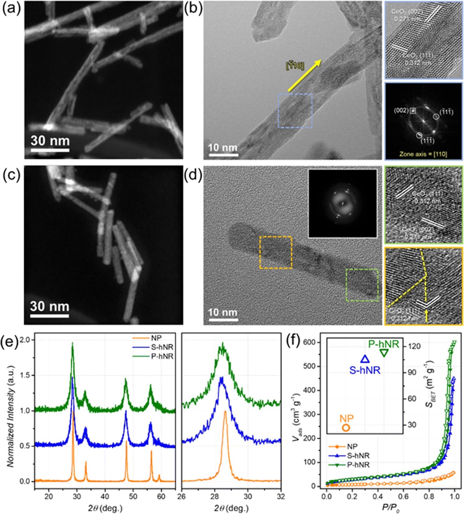 | ||
| Fig. 1 (a) STEM image of CeO2−x S-hNR. (b) HRTEM image of CeO2−x S-hNR (left) and enlarged HRTEM image and corresponding FFT patterns of the marked area (right). (c) STEM image of CeO2−x P-hNR. (d) HRTEM image of CeO2−x P-hNR (left) and enlarged HRTEM images of the marked area (right). (e) PXRD patterns of CeO2−x S-hNR, P-hNR, and commercial CeO2 nanoparticles (NP) and enlarged PXRD patterns from 26° to 32° (right). (f) N2-isotherm curves of CeO2−x S-hNR, P-hNR, and NP and the calculated BET surface area of the samples (inset). | ||
The crystallinity of the hollow nanotube structures was further investigated using high-resolution TEM (HRTEM) images and corresponding fast Fourier transform (FFT) patterns, as shown in Fig. 1b and d. The HRTEM analysis shown in Fig. 1b showed lattice distances of 0.312 and 0.271 nm, which correspond to the lattice distances of the (002) and (1![[1 with combining macron]](https://www.rsc.org/images/entities/char_0031_0304.gif) ) facets of the cubic CeO2, respectively. Also, the corresponding FFT pattern indicated that the observed zone axis of the HRTEM image is [110], verifying that most of the exposed facets of CeO2−x S-hNR are (110) and the overall nanostructure possess single-crystalline nature. On the other hand, according to the HRTEM image (Fig. 1d) and the corresponding FFT patterns (inset) of CeO2−x P-hNR, grain boundaries (yellow dotted lines) were observed, while the measured lattice distances (0.312 and 0.271 nm) were the same as those of CeO2−x S-hNR.
) facets of the cubic CeO2, respectively. Also, the corresponding FFT pattern indicated that the observed zone axis of the HRTEM image is [110], verifying that most of the exposed facets of CeO2−x S-hNR are (110) and the overall nanostructure possess single-crystalline nature. On the other hand, according to the HRTEM image (Fig. 1d) and the corresponding FFT patterns (inset) of CeO2−x P-hNR, grain boundaries (yellow dotted lines) were observed, while the measured lattice distances (0.312 and 0.271 nm) were the same as those of CeO2−x S-hNR.
The powder X-ray diffraction (PXRD) patterns of CeO2−x S-hNR and CeO2−x P-hNR demonstrated that the phase of those two nanorods were the cubic CeO2 phase (Fig. 1e). The average crystallite domain sizes of the samples were calculated using the Scherrer equation, with PXRD peaks near 28.5°.25 The calculated average crystallite sizes of CeO2−x S-hNR, CeO2−x P-hNR, and commercial CeO2 nanoparticles (NPs) were 13.4 ± 0.3, 11.1 ± 0.3, and 39.0 ± 0.9 nm, respectively. The calculated crystallite sizes of commercial CeO2 NPs by Scherrer equation were similar to the sizes of those observed in the TEM image, as shown in Fig. S3 (ESI†).
Also, the PXRD patterns of S-hNR and P-hNR were slightly negative-shifted compared to that of the NP, which indicates the crystal lattices in the hollow structure were slightly expanded to bulk phase. The expanded crystal lattice was attributed to the decrease in crystallite domain size, which increased the surface concentration of oxygen vacancies and Ce3+ states in the nanocrystal.26,27
N2 isotherms (Fig. 1f) of CeO2−x S-hNR, CeO2−x P-hNR, and commercial CeO2 NP samples were measured at −196 °C to calculate their BET surface areas (SBET). The surface areas of the CeO2−x S-hNR (104.80 m2 g−1) and CeO2−x P-hNR (113.87 m2 g−1) were much higher than that of CeO2 NP (26.99 m2 g−1). Also, the SBET of those hNRs was higher than the non-porous CeO2−x nanorods (94.26 m2 g−1, Fig. S4, ESI†), indicating that the increased surface areas originate from the inner cavity in the nanorod structure. In particular, because the CeO2−x P-hNR has a larger number of defect structures and pores along multiple grain boundaries, it showed higher SBET than the CeO2−x S-hNR.
The radical scavenging efficiencies of the CeO2−x samples were evaluated by dye tests, using the chemical degradation of methyl violet 2B (MV) in Fenton's solution (˙OH radical source) over 90 min (Fig. S5, ESI†).24 The concentration of radical scavenger in the reaction solution was fixed to 0.091 mgCe mL−1 (see experimental section for details). The radical scavenging efficiency was evaluated by the change in the absorption peak intensity of MV dye at 575 nm. The normalized peak intensity change over time is summarized in Fig. 2a. The addition of CeO2 or CeO2−x decreased the degradation rate of the MV dye regardless of their structure, confirming that they can efficiently scavenge ˙OH radicals. Without radical scavengers, the absorption intensity of MV dye in the solution remained at 34.6% of the initial state after 90 min. However, the final absorption intensity remained at 69.7%, 70.3%, and 58.1% of the initial state following the addition of CeO2−x S-hNR, CeO2−x P-hNR, and commercial CeO2 NP, respectively. This indicates that the hollow nanorod structures have higher radical scavenging efficiency than commercial NPs regardless of their initial crystallinity.
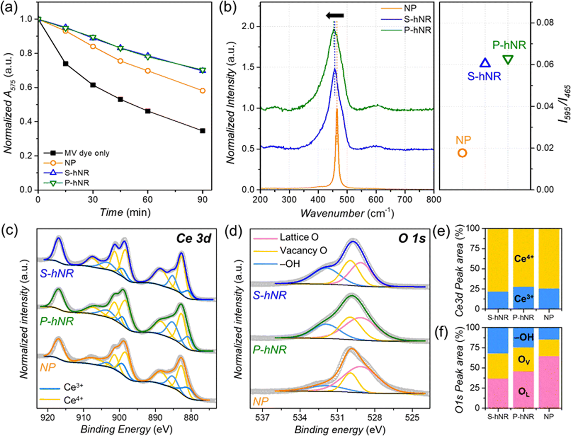 | ||
| Fig. 2 (a) Hydroxyl radical scavenging efficiency measurement of the CeO2−x-based radical scavengers. Change in absorption intensity at 575 nm over time in the presence of MV dye and radical scavengers after injecting Fenton's reagent. (b) Raman spectra of CeO2−x S-hNR, CeO2−x P-hNR, and commercial CeO2 NP, normalized to F2g band near 465 cm−1 for clarity. The right graph indicates the peak intensity ratio between 595 cm−1 and 465 cm−1. (c) Ce 3d XPS spectra (d) O 1s XPS spectra of CeO2−x S-hNR, CeO2−x P-hNR, and commercial CeO2 NP. (e and f) Relative peak area from the deconvoluted (e) Ce 3d and (f) O 1s XPS spectra in (c and d), respectively. | ||
The chemical states of the CeO2−x structures were next investigated by Raman spectroscopy (Fig. 2b) to determine the origin of the improved radical scavenging activity of the CeO2−x S-hNR and CeO2−x P-hNR. It has been reported that perfect CeO2 crystal without any oxygen vacancies shows only a single Raman active mode with F2g symmetry at 465 cm−1.28 For the three CeO2−x samples, a single major peak near 465 cm−1 was observed. However, a red shift of the major peak was observed in both the CeO2−x S-hNR and CeO2−x P-hNR samples, compared to the commercial CeO2 NP. This red shift largely originates from partially reduced states (Ce3+) and the lattice expansion of the CeO2 lattice,29 which corroborates with the PXRD results in Fig. 1e. Moreover, in the Raman spectra of CeO2−x S-hNR and CeO2−x P-hNR showed asymmetric broadening of the 465 cm−1 peak and minor peak around 595 cm−1. These features are related to the breaking of F2g symmetry by the formation of oxygen vacancies in the CeO2−x crystal.28,30 Because the Raman peak at 595 cm−1 is a defect-induced mode,31 the relative intensities (I595/I465) of the 465 and 595 cm−1 bands were compared. The I595/I465 value of CeO2−x P-hNR (0.063) was slightly larger than that of CeO2−x S-hNR (0.060) and much larger than that of CeO2 NP (0.018). Therefore, the multiple grain boundaries in CeO2−x P-hNR enabled a higher concentration of surface oxygen vacancies in their structure. However, because the surface area and small crystallite size were comparable, the surface oxygen vacancy concentration of CeO2−x S-hNR is comparable to that of CeO2−x P-hNR.
XPS spectra were also measured to further investigate the chemical states of the CeO2−x hNRs (Fig. 2c–f). The surface concentration of Ce3+ and Ce4+ states were evaluated by deconvoluting the Ce 3d XPS spectra (Fig. 2c and Table S1, ESI†) of the samples. The calculated ratios of the Ce3+ state were in the following order (Fig. 2e): CeO2−x S-hNR (21.9%) < CeO2 NP (25.5%) < CeO2−x P-hNR (28.0%). Because the CeO2−x P-hNRs had multiple grain boundaries and defect sites in their structure, they possessed the highest concentration of Ce3+ states, which are known to be active species toward ˙OH radical scavenging. The states of the surface oxygen species in the samples were also evaluated by O 1s XPS spectra (Fig. 2d). The deconvolution result (Fig. 2f) showed the ratio of oxygen species near the vacant sites (vacancy O, OV) in CeO2−x S-hNR (31.3%) and CeO2−x P-hNR (29.9%) was higher than that of CeO2 NP (20.6%), corroborating the Raman spectra (Fig. 2b).
It has been well known that the Ce3+ state is an active species for ˙OH radical scavenging.32–37 However, while the CeO2−x S-hNRs possessed the lowest surface concentration of Ce3+ species, they showed radical scavenging efficiency that was comparable to the CeO2−x P-hNRs. Therefore, the superior ˙OH radical scavenging performances of CeO2−x S-hNR and CeO2−x P-hNR are mainly due to their high surface area.
However, the change in surface states with the increased surface concentration of oxygen vacancies and Ce3+ states could also have an effect on their radical scavenging activity. Because the CeO2−x S-hNR samples still possess a higher surface concentration of oxygen vacancies than the other samples, these can also improve the ˙OH radical scavenging activity.
3.2. OPV device preparation and characterization
Zinc oxide (ZnO) is one of the most widely used materials for the electron transport layer in the inverted OPV cell architecture.38–41 ZnO layers are typically developed using a sol–gel-based solution42 and ZnO nanoparticle solution43 due to the ease of film formation with low annealing temperature and highly reproducible film quality. However, it is also widely known that hydroxyl radicals (˙OH) can form when ZnO film with H2O on its surface is exposed to UV irradiation,16 and the generated radicals can decompose the active film, especially the non-fullerene acceptor (NFA) molecules, at the ZnO/active layer interface.17 Therefore, if the hydroxyl radicals generated by UV exposure can be efficiently eliminated, one could see a considerable enhancement in the operational stability of the resulting ZnO-based inverted OPVs.We introduced CeO2−x S-hNR, CeO2−x P-hNR, and commercial CeO2 NP to the ZnO film in the inverted OPV structure of indium tin oxide (ITO)/ZnO/active layer/MoO3/Ag. Prior to application to the OPV architecture, we first investigated the coating behaviour of the CeO2−x films on ZnO using a scanning electron microscope (SEM). Fig. S6 (ESI†) show the SEM images of NP, S-hNR, and P-hNR films on ZnO films, respectively, and Fig. S7 (ESI†) are the elemental mapping images of the Ce line in the above SEM images. As observed, there are aggregates consisting of cerium oxides, regardless of the crystallinity of cerium oxide. However, the CeO2−x S-hNR-based film had the most homogeneous coverage of the ZnO film with the smallest aggregates. Considering that such aggregations can act as pinholes in active film, and this could lead to a short circuit in an OPV device, we expect that CeO2−x S-hNR-based OPVs show better and more reproducible photovoltaic properties.
Then we introduced various cerium oxide layers between the ZnO layer and active layer in the OPV structure. As seen in Fig. S8 (ESI†), the cerium oxide layers fully cover the spiky surface of ZnO with reduced root-mean-square roughness (Rrms) values, irrespective of the crystallinity of cerium oxide. The measured thickness values of cerium oxide layers were ∼10 nm, regardless of their crystallinity (Fig. S9, ESI†). To confirm the effect of CeO2−x nanoparticle aggregations on the morphology of active films, we observed the morphology of a thin (∼40 nm) active film on ZnO or ZnO/CeO2−x films using an atomic force microscope (AFM). The topography images can be found in Fig. 3a–d. Although small aggregates are shown in all the active films on the CeO2−x layers, their root-mean-square roughness values were nearly the same, ranging from 0.84 to 1.05 nm. Therefore, we speculated that the aggregates in the active films would not significantly affect the device performance.
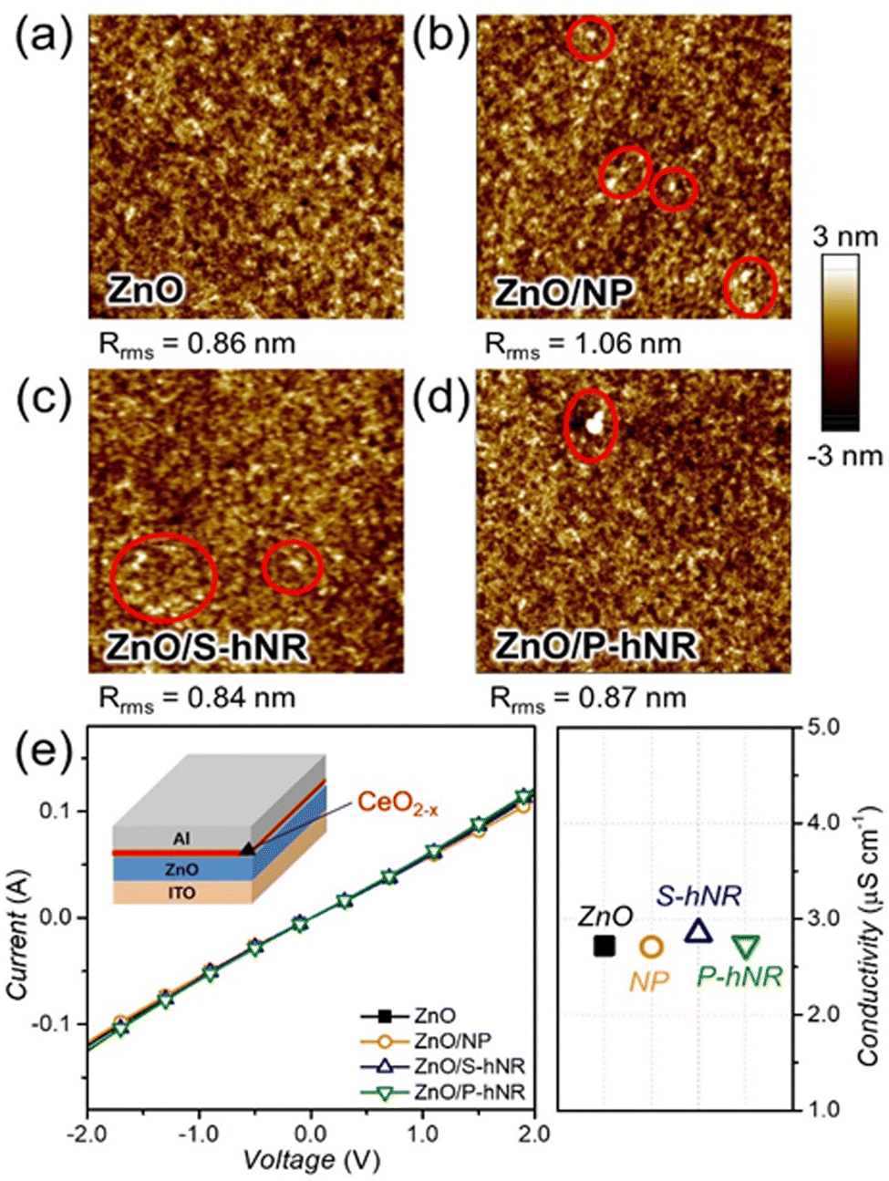 | ||
| Fig. 3 (a–d) AFM topography images (5 μm × 5 μm) of thin (∼40 nm) PM6:N3 bled films on (a) ZnO, (b) ZnO/CeO2 NP, (c) ZnO/CeO2−x S-hNR, and (d) ZnO/CeO2−x P-hNR layers. The red circles in the images indicate the aggregations in the films. (e) The I–V curves of ITO/ZnO/Al or ITO/ZnO/CeO2−x/Al sandwiched devices for measuring the conductivity of ZnO or ZnO/CeO2−x layers. Inset: Schematic illustration of the device configuration for conductivity measurements. The right graph indicates the calculated conductivity by the I–V curve. | ||
Before fabricating the OPV cells, we tested the effect of CeO2−x layers on the conductivity of the ZnO layers. The current–voltage (I–V) curves of the ITO/ZnO/Al or ITO/ZnO/CeO2−x/Al sandwiched devices were measured, and the I–V curves and the calculated conductivity values can be found in Fig. 3e. The calculated conductivity values were similar, with a range of 2.7 to 2.8 μS cm−1, regardless of the presence of CeO2−x layers. Therefore, we can expect that the introduction of CeO2−x layers would not lead to a decrease in the electrical properties of the OPV structure. However, it was also found that the introduction of too thick cerium oxide layer can lead to a slight deterioration in electrical conductivity, because the electrical property of cerium oxide is not as good as that of ZnO (Fig. S10, ESI†).
Then, we fabricated inverted OPV cells with a structure of ITO/ZnO/CeO2−x/active layer/MoO3/Ag (Fig. 4a). The J–V characteristics and external quantum efficiency (EQE) spectra of the resultant OPVs can be found in Fig. 4b and c, respectively, and the photovoltaic parameters are summarized in Table S2 (ESI†). As we expected above, the fabricated OPVs showed device performance similar to the PCEs, ranging from 14.6 to 15.0% with similar shapes of EQE spectra (Fig. 4c), irrespective of the types of CeO2−x nanostructures.
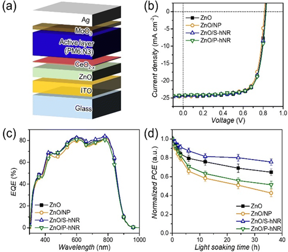 | ||
| Fig. 4 (a) Schematic illustration of the OPV device. (b) J–V characteristics and (c) external quantum efficiency (EQE) spectra of the OPVs with various CeO2−x-based interlayers and (d) their dependency of normalized average PCE on light soaking time under 1 sun condition. | ||
Based on the fabricated CeO2−x-integrated OPV cells, we tested the photostability of the OPV cells. The OPVs were encapsulated to prevent any additional degradation by oxygen and water in air. The encapsulated OPVs were exposed to 1 sun condition up to 36 hours and the device performances were recorded at selected light soaking times (Fig. S11, ESI†). The dependency of PCEs on light soaking time is summarized in Fig. 4d and dependencies of other photovoltaic parameters such as JSC, VOC and FF can be found in Fig. S12 (ESI†).
Interestingly, only the OPV with CeO2−x S-hNR layer showed better photostability than that of ZnO-based reference OPV, and the device performances of CeO2 NP- and CeO2−x P-hNR-based OPVs were even worse than that of the reference OPV. The ZnO only, CeO2 NP-, CeO2−x P-hNR- and CeO2−x S-hNR-based OPV devices decreased their average PCEs to −35.3%, −57.3%, −48.6%, and −24.4% of their initial efficiencies after 36 h of light exposure, respectively. All the photovoltaic parameters of the CeO2 NP- or CeO2−x P-hNR- based OPV cells showed faster decreases than those of ZnO- or CeO2−x S-hNR-based OPVs (Fig. S12, ESI†). To confirm the effect of UV light on photostability of the OPVs, the photostability test was repeated using ZnO- and ZnO/CeO2−x S-hNR-based OPV cells under 1 sun condition. By attaching polyimide films to backside of the OPV cells, the incident UV light in solar spectrum can be effectively excluded (Fig. S13a, ESI†). As shown in Fig. S13b (ESI†), this photostability was clearly improved regardless of the presence of CeO2−x layers. This result indicates that the photostability issues are mainly related to the hydroxyl radical generated by photocatalysis under UV exposure. As mentioned above, since the generated hydroxyl radicals can attack active materials, the cerium oxide layers in the OPV structure acted as radical scavengers against hydroxyl radicals, thereby suppressing the decomposition of the active layer. However, as being revealed from the analyses using SEM (Fig. S6, ESI†) and AFM images (Fig. 3a–d and Fig. S8, ESI†), CeO2−x S-hNR formed uniform deposition on the ZnO film, in contrast with CeO2 NP and CeO2−x P-hNR films which were rough and showed large aggregates. It is widely known that the morphology of the active film deposited on a rough surface are more labile than that on a smooth surface by external stimulus, which can accelerate the degradation of OPV devices, especially for the initial step of degradation (burn-in degradation).10
3.3. Stability enhancement mechanism of CeO2−x in the interlayer
To elucidate the reason why the CeO2−x S-hNR-based OPVs showed better photostability, we collected the absorption spectra of PM6:N3 blend films on ZnO or ZnO/CeO2−x layers after various exposure times to UV. The PM6:N3 blend films were fabricated with an ultrathin thickness of ∼10 nm to observe the aspects occurring at the ZnO/active layer or the CeO2−x/active layer interface more directly. Fig. S14 (ESI†) shows the evolution of UV-visible absorption spectra under various UV exposure times up to 6 min. As UV exposure time increases, one can clearly see that the absorption peak near 780 nm gradually decreases. Considering the absorption spectra of PM6 and N3 (Fig. S15, ESI†), the absorption peak near 780 nm is related to the absorption of N3. The trend in absorption of blend films on various layers is summarized in Fig. 5a.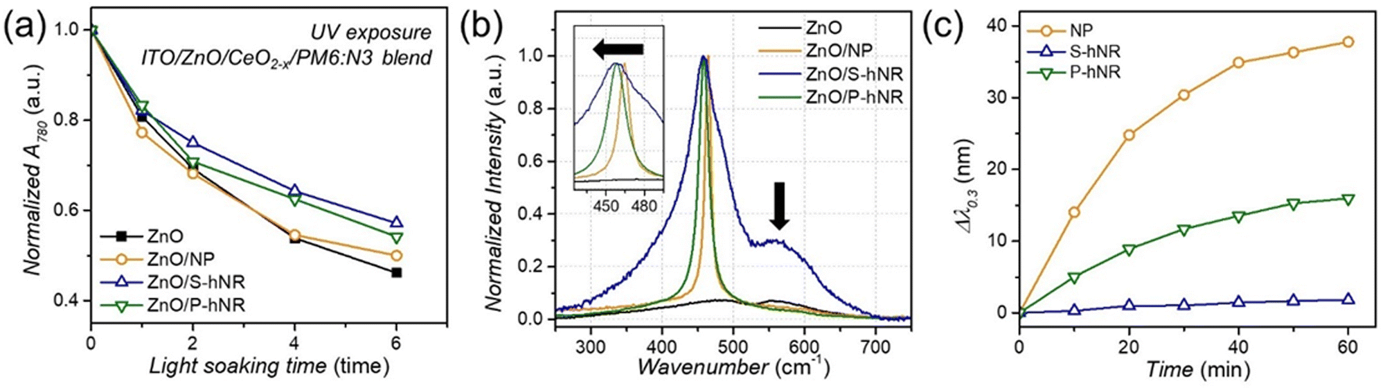 | ||
| Fig. 5 (a) Change in the intensity of 780 nm absorption peaks of the UV-visible absorption spectra (Fig. S14, ESI†) of thin PM6:N3 blend films on ZnO, ZnO/CeO2 NP, ZnO/CeO2−x S-hNR, and ZnO/CeO2−x P-hNR layers under the UV exposure. (b) Raman spectra of ZnO, ZnO/CeO2 NP, ZnO/CeO2−x S-hNR, and ZnO/CeO2−x P-hNR films, normalized to F2g band near 465 cm−1. (c) Wavelength change at the optical density of 0.30 of the UV-visible absorption spectra (Fig. S16, ESI†) of CeO2−x-based aqueous dispersion (695 mM) after injection of H2O2 (5 μmol), related to the catalytic degradation of H2O2 by surface redox reaction of CeO2−x nanostructures. | ||
For the blend film on the ZnO layer, the absorption peak near 780 nm was decreased by −53.8% after 6 min of UV exposure. However, with the blend films on CeO2−x layers, relatively small decreases of −50%, −45.9%, and −42.9% were exhibited by the blend films on the CeO2 NP, CeO2−x P-hNR and CeO2−x S-hNR layers, respectively.
For the absorption peak near 620 nm, which is related to the absorption of PM6, the absorption decreased by less than 10%, irrespective of the presence of cerium oxide layers. Therefore, we can conclude that the decrease in light absorption efficiency due to the degradation of N3 molecules is one of the main reasons for deterioration in PCE. N3 can be decomposed by the attack of ˙OH radicals generated from ZnO layer to vinyl linkers. Since the conjugation in the decomposed N3 molecules are broken, they cannot act as electron acceptor anymore, resulting in poor electron transfer from N3 to ZnO. However, CeO2−x can suppress those ˙OH radicals by radical scavenging mechanism,37 thereby enhancing the photostability of the resultant OPV cells.
Although the CeO2−x S-hNR and the CeO2−x P-hNR showed similar radical scavenging activity in solution phase (Fig. 2a), the OPV device with the CeO2−x S-hNR interlayer showed higher stability against ˙OH radicals. To elucidate the difference in radical scavenging activity between solution phase and device, we furtherly investigated the states of the CeO2−x based radical scavengers when they were located on ZnO film surfaces.
The Raman spectra (Fig. 5b) of ZnO/CeO2−x films on ITO glass revealed that the ZnO/CeO2−x S-hNR film had a much broader band shape and much larger red shift in the F2g band (465 cm−1) than the ZnO/CeO2−x P-hNR film. Also, the intensity of the 595 cm−1 bands in the ZnO/CeO2−x S-hNR film was much higher than those of the ZnO/CeO2−x P-hNR and ZnO/CeO2 NP films. This indicates that the CeO2−x S-hNR possessed more surface Ce3+ states with defect structures,44 which are active toward ˙OH radical quenching, than the CeO2−x P-hNR when they formed films on the ZnO surface.
Moreover, as observed in the SEM (Fig. S6, ESI†) and AFM (Fig. 3c) analyses, the CeO2−x S-hNR-based film had the best coverage on ZnO film. Therefore, we suppose that on the ZnO film, the CeO2−x S-hNR can effectively quench ˙OH radicals generated from photocatalytic reactions on the ZnO surfaces. This occurs because they can effectively form interfaces on the ZnO surface. For the ZnO/CeO2−x P-hNR (Fig. 3d), on the other hand, several aggregations were observed due to the severe aggregation of CeO2−x P-hNR radical scavengers. As a result, the interfacial CeO2−x P-hNR on the ZnO film could not effectively form an interface with the ZnO, and failed to rapidly quench ˙OH radicals generated from the ZnO layer.
It has been reported that CeO2−x nanostructures can also possess pro-oxidant properties generating reactive oxygen species under a certain environment rather showing radical-scavenging activity.35,45 Therefore, accelerated degradation of OPV devices with CeO2 NP and CeO2−x P-hNR interlayer might originate from the unwanted side redox reaction on the surface of the CeO2−x. To elucidate this, we observed the catalytic H2O2 degradation activity of the three CeO2−x nanostructures, which can be measured by the change in UV-vis spectra of an aqueous dispersion of CeO2−x after injection of H2O2 (Fig. S16, ESI†).46 In particular, the change in wavelength at the optical density of 0.30, related to the generation of Ce3+ species from the surface Ce4+ states, is the indicator of the H2O2 decomposition activity. As shown in Fig. 5c, the wavelength change was found to be in the order of CeO2 NP > CeO2−x P-hNR > CeO2−x S-hNR. This trend corroborates with OPV results (Fig. 4d), where the CeO2 NP-based device showed the most rapid degradation rate of the average PCE.
While the exact reaction mechanism is still in debate, the reaction of CeO2−x with H2O2 can undergo both anti-oxidative (superoxide dismutase- or catalase-like activity) and pro-oxidative (oxidase- or peroxidase-like activity).45,47 In our case, the trends observed in the change in UV-vis spectra are well with the OPV results – the CeO2−x S-hNR, which showed the smallest change in optical density after injecting H2O2, only exhibited higher OPV device stability. However, the CeO2 NP and CeO2−x P-hNR-based OPV showed inferior stability to the ZnO-only OPV device without CeO2−x-based interlayer. Those two nanostructures showed higher activity toward the generation of the Ce3+ state via catalytic H2O2 decomposition, which was observed by the UV-vis spectra. In this case, we suppose that the H2O2 decomposition reaction underwent oxidase- or peroxidase-like mechanisms, thereby generating reactive oxygen species. Therefore, it seems that the surface regeneration of the Ce4+ to Ce3+ state is also a key factor for the performance of radical-scavenging CeO2−x-based interlayers for OPV applications.
4. Conclusions
In conclusion, we demonstrated the ability of CeO2−x nanostructures to mitigate the photodegradation process in OPV devices by measuring the scavenging effect of hydroxyl radicals with a focus on the influence of morphology and crystallinity. Material characterization and analyses of device test results revealed that as a radical scavenger the S-hNR nanostructured CeO2−x was very effective in OPV devices and was responsible for the higher surface concentration of Ce3+ and the interfacial compatibility between constituent layers, which all contributed to radical scavenging.Author contributions
Seongwon Yoon: conceptualization, methodology, investigation, visualization, writing-original draft. Taehyun Kwon: conceptualization, methodology, investigation, visualization, writing-original draft. Sohyun Kim: investigation, visualization. So Hyun Park: investigation. Youngjoon Lim: investigation, validation. Jihun Kim: investigation. Jun Kim: validation. Kwangjin An: validation. Sungmin Park: investigation, writing-original draft. Jin Young Kim: conceptualization, methodology, supervision, funding acquisition, writing-review & editing. Hae Jung Son: conceptualization, methodology, supervision, funding acquisition, project administration, writing-review & editing.Conflicts of interest
There are no conflicts of interest to declare.Acknowledgements
This work was supported by the program of Future Hydrogen Original Technology Development (NRF-2021M3I3A1082879) through the National Research Foundation of Korea (NRF) funded by the Korean government (Ministry of Science and ICT), the Korea Institute Energy Technology Evaluation and Planning (KETEP) grant funded by the Korea government (MOTIE) (no. 20213030030260), and KIST Institutional Program (2E31871). This work was also supported by the National R & D Program through the NRF of Korea funded by the Ministry of Science and ICT (NRF-2020M3H4A1A02084910), and the Nano Future Material Technology Development Program through the NRF of Korea funded by the Ministry of Science and ICT (NRF-2020M3H4A3081817). T. K. acknowledges the NRF of Korea grant funded by the Korea government (MSIT) (No. 2022R1C1C2004703).References
- G. Zhang, F. R. Lin, F. Qi, T. Heumuller, A. Distler, H. J. Egelhaaf, N. Li, P. C. Y. Chow, C. J. Brabec, A. K. Jen and H. L. Yip, Chem. Rev., 2022, 122, 14180–14274 CrossRef CAS PubMed.
- P. Xue, P. Cheng, R. P. S. Han and X. Zhan, Mater. Horiz., 2022, 9, 194–219 RSC.
- S. Yoon, E. Y. Shin, N. K. Cho, S. Park, H. Y. Woo and H. J. Son, J. Mater. Chem. A, 2021, 9, 24729–24758 RSC.
- Y. Cui, Y. Xu, H. Yao, P. Bi, L. Hong, J. Zhang, Y. Zu, T. Zhang, J. Qin, J. Ren, Z. Chen, C. He, X. Hao, Z. Wei and J. Hou, Adv. Mater., 2021, 33, e2102420 CrossRef PubMed.
- P. Bi, S. Zhang, Z. Chen, Y. Xu, Y. Cui, T. Zhang, J. Ren, J. Qin, L. Hong, X. Hao and J. Hou, Joule, 2021, 5, 2408–2419 CrossRef CAS.
- Y. Wei, Z. Chen, G. Lu, N. Yu, C. Li, J. Gao, X. Gu, X. Hao, G. Lu, Z. Tang, J. Zhang, Z. Wei, X. Zhang and H. Huang, Adv. Mater., 2022, 34, e2204718 CrossRef PubMed.
- W. Gao, F. Qi, Z. Peng, F. R. Lin, K. Jiang, C. Zhong, W. Kaminsky, Z. Guan, C. S. Lee, T. J. Marks, H. Ade and A. K. Jen, Adv. Mater., 2022, 34, e2202089 CrossRef PubMed.
- Z. Zheng, J. Wang, P. Bi, J. Ren, Y. Wang, Y. Yang, X. Liu, S. Zhang and J. Hou, Joule, 2022, 6, 171–184 CrossRef CAS.
- S. Park, T. Kim, S. Yoon, C. W. Koh, H. Y. Woo and H. J. Son, Adv. Mater., 2020, 32, e2002217 CrossRef PubMed.
- L. Duan and A. Uddin, Adv. Sci., 2020, 7, 1903259 CrossRef CAS PubMed.
- P. Cheng and X. Zhan, Chem. Soc. Rev., 2016, 45, 2544–2582 RSC.
- J. Guo, Y. Wu, R. Sun, W. Wang, J. Guo, Q. Wu, X. F. Tang, C. K. Sun, Z. H. Luo, K. Chang, Z. H. Zhang, J. Yuan, T. F. Li, W. H. Tang, E. J. Zhou, Z. Xiao, L. M. Ding, Y. P. Zou, X. W. Zhan, C. L. Yang, Z. Li, C. J. Brabec, Y. F. Li and J. Min, J. Mater. Chem. A, 2019, 7, 25088–25101 RSC.
- Y. S. Zhao, Z. N. Wu, X. Liu, Z. P. Zhong, R. H. Zhu and J. S. Yu, J. Mater. Chem. C, 2021, 9, 13972–13980 RSC.
- Y. Y. Jiang, L. L. Sun, F. Y. Jiang, C. Xie, L. Hu, X. Y. Dong, F. Qin, T. F. Liu, L. Hu, X. S. Jiang and Y. H. Zhou, Mater. Horiz., 2019, 6, 1438–1443 RSC.
- A. Uddin and H. M. Yi, Sol. RRL, 2022, 6, 2100983 CrossRef CAS.
- Z. M. Wang, K. Wang, H. Wang, X. Chen, W. X. Dai and X. Z. Fu, Catal. Sci. Technol., 2018, 8, 3260–3277 RSC.
- S. Park and H. J. Son, J. Mater. Chem. A, 2019, 7, 25830–25837 RSC.
- Y. Wang, Z. Zheng, J. Wang, X. Liu, J. Ren, C. An, S. Zhang and J. Hou, Adv. Mater., 2022, e2208305 CrossRef PubMed.
- A. Soultati, A. Fakharuddin, E. Polydorou, C. Drivas, A. Kaltzoglou, M. I. Haider, F. Kournoutas, M. Fakis, L. C. Palilis, S. Kennou, D. Davazoglou, P. Falaras, P. Argitis, S. Gardelis, A. Kordatos, A. Chroneos, L. Schmidt-Mende and M. Vasilopoulou, ACS Appl. Energy Mater., 2019, 2, 1663–1675 CrossRef CAS.
- F. Cao, M. Zhang, K. Yang, Z. Tian, J. Li and Y. Qu, Nano Res., 2020, 14, 715–719 CrossRef.
- S. Zhang, Z. Q. Huang, Y. Ma, W. Gao, J. Li, F. Cao, L. Li, C. R. Chang and Y. Qu, Nat. Commun., 2017, 8, 15266 CrossRef CAS PubMed.
- H. X. Mai, L. D. Sun, Y. W. Zhang, R. Si, W. Feng, H. P. Zhang, H. C. Liu and C. H. Yan, J. Phys. Chem. B, 2005, 109, 24380–24385 CrossRef CAS PubMed.
- J. Li, Z. Y. Zhang, Z. M. Tian, X. M. Zhou, Z. P. Zheng, Y. Y. Ma and Y. Q. Qu, J. Mater. Chem. A, 2014, 2, 16459–16466 RSC.
- Y. Xue, Q. F. Luan, D. Yang, X. Yao and K. B. Zhou, J. Phys. Chem. C, 2011, 115, 4433–4438 CrossRef CAS.
- A. L. Patterson, Phys. Rev., 1939, 56, 978–982 CrossRef CAS.
- S. Deshpande, S. Patil, S. V. N. T. Kuchibhatla and S. Seal, Appl. Phys. Lett., 2005, 87, 133113 CrossRef.
- X. Hao, A. Yoko, C. Chen, K. Inoue, M. Saito, G. Seong, S. Takami, T. Adschiri and Y. Ikuhara, Small, 2018, 14, e1802915 CrossRef PubMed.
- R. Schmitt, A. Nenning, O. Kraynis, R. Korobko, A. I. Frenkel, I. Lubomirsky, S. M. Haile and J. L. M. Rupp, Chem. Soc. Rev., 2020, 49, 554–592 RSC.
- Y. Lee, G. He, A. J. Akey, R. Si, M. Flytzani-Stephanopoulos and I. P. Herman, J. Am. Chem. Soc., 2011, 133, 12952–12955 CrossRef CAS PubMed.
- C. Schilling, A. Hofmann, C. Hess and M. V. Ganduglia-Pirovano, J. Phys. Chem. C, 2017, 121, 20834–20849 CrossRef CAS.
- Z. Wu, M. Li, J. Howe, H. M. Meyer, 3rd and S. H. Overbury, Langmuir, 2010, 26, 16595–16606 CrossRef CAS PubMed.
- A. Filippi, F. Liu, J. Wilson, S. Lelieveld, K. Korschelt, T. Wang, Y. Wang, T. Reich, U. Poschl, W. Tremel and H. Tong, RSC Adv., 2019, 9, 11077–11081 RSC.
- T. Kwon, Y. Lim, J. W. Cho, R. Lawler, B. J. Min, W. A. Goddard, S. S. Jang and J. Y. Kim, Mater. Today, 2022, 58, 135–163 CrossRef CAS.
- T. Kwon, S. H. Park, B. J. Min, S. Park, S. Ramadhani, Y. Lim, S. S. Jang, H. Jeong, H. J. Son and J. Y. Kim, Adv. Energy Sustainability Res., 2022, 3, 2200011 CrossRef.
- M. S. Lord, J. F. Berret, S. Singh, A. Vinu and A. S. Karakoti, Small, 2021, 17, e2102342 CrossRef PubMed.
- K. J. Mitchell, J. L. Goodsell, B. Russell-Webster, U. T. Twahir, A. Angerhofer, K. A. Abboud and G. Christou, Inorg. Chem., 2021, 60, 1641–1653 CrossRef CAS PubMed.
- V. Prabhakaran, C. G. Arges and V. Ramani, Proc. Natl. Acad. Sci. U. S. A., 2012, 109, 1029–1034 CrossRef CAS PubMed.
- J. Yuan, Y. Zhang, L. Zhou, G. Zhang, H.-L. Yip, T.-K. Lau, X. Lu, C. Zhu, H. Peng, P. A. Johnson, M. Leclerc, Y. Cao, J. Ulanski, Y. Li and Y. Zou, Joule, 2019, 3, 1140–1151 CrossRef CAS.
- C. Li, J. Zhou, J. Song, J. Xu, H. Zhang, X. Zhang, J. Guo, L. Zhu, D. Wei, G. Han, J. Min, Y. Zhang, Z. Xie, Y. Yi, H. Yan, F. Gao, F. Liu and Y. Sun, Nat. Energy, 2021, 6, 605–613 CrossRef CAS.
- Y. Cui, H. Yao, J. Zhang, T. Zhang, Y. Wang, L. Hong, K. Xian, B. Xu, S. Zhang, J. Peng, Z. Wei, F. Gao and J. Hou, Nat. Commun., 2019, 10, 2515 CrossRef PubMed.
- S. Yoon, S. Park, S. H. Park, S. Nah, S. J. Lee, J. W. Lee, H. Ahn, H. Y. G. Yu, E. Y. Shin, B. J. Kim, B. K. Min, J. H. Noh and H. J. Son, Joule, 2022, 6, 2406–2422 CrossRef CAS.
- Y. Sun, J. H. Seo, C. J. Takacs, J. Seifter and A. J. Heeger, Adv. Mater., 2011, 23, 1679–1683 CrossRef CAS PubMed.
- S. K. Hau, H. L. Yip, N. S. Baek, J. Y. Zou, K. O'Malley and A. K. Y. Jen, Appl. Phys. Lett., 2008, 92, 253301 CrossRef.
- S. Loridant, Catal. Today, 2021, 373, 98–111 CrossRef CAS.
- V. Baldim, N. Yadav, N. Bia, A. Graillot, C. Loubat, S. Singh, A. S. Karakoti and J.-F. Berret, ACS Appl. Mater. Interfaces, 2020, 12, 42056–42066 CrossRef CAS PubMed.
- S. S. Lee, W. Song, M. Cho, H. L. Puppala, P. Nguyen, H. Zhu, L. Segatori and V. L. Colvin, ACS Nano, 2013, 7, 9693–9703 CrossRef CAS PubMed.
- T. J. Fisher, Y. Zhou, T.-S. Wu, M. Wang, Y.-L. Soo and C. L. Cheung, Nanoscale, 2019, 11, 4552–4561 RSC.
Footnotes |
| † Electronic supplementary information (ESI) available. See DOI: https://doi.org/10.1039/d2tc04152a |
| ‡ These authors contributed equally. |
| This journal is © The Royal Society of Chemistry 2023 |