
Advanced atomic layer deposition: metal oxide thin film growth using the discrete feeding method†
Jae Chan
Park
a,
Chang Ik
Choi
a,
Sang-Gil
Lee
b,
Seung Jo
Yoo
b,
Ji-Hyun
Lee
b,
Jae Hyuck
Jang
b,
Woo-Hee
Kim
 a,
Ji-Hoon
Ahn
a,
Jeong Hwan
Kim
*c and
Tae Joo
Park
*a
a,
Ji-Hoon
Ahn
a,
Jeong Hwan
Kim
*c and
Tae Joo
Park
*a
aDepartment of Materials Science and Chemical Engineering, Hanyang University, Ansan 15588, Republic of Korea. E-mail: tjp@hanyang.ac.kr
bCenter for Research Equipment, Korea Basic Science Institute, Daejeon 34133, Republic of Korea
cDepartment of Materials Science and Engineering, Hanbat National University, Daejeon 34158, Republic of Korea. E-mail: jkim@hanbat.ac.kr
First published on 12th December 2022
Abstract
A HfO2 film was grown via atomic layer deposition (ALD) with a discrete feeding method (DFM), called DF-ALD, and its physical, chemical, and electrical properties were studied. In conventional ALD processes, even in the growth saturation condition, not all substrate surface reactive sites react with precursor or reactant molecules because physisorbed precursor and byproduct molecules screen the subjacent surface reactive sites. The DF-ALD process in this work employed divided precursor feeding and purging steps in the growth saturation condition of a control ALD process, such that the divided steps efficiently eliminated the physisorbed precursor molecules or by-products screening the subjacent surface reactive sites. This increased the adsorption and filling efficiency of the precursor molecules onto the substrate or film surface during deposition. As a result, the DF-ALD increased the film density and reduced the interfacial layer thickness which degrades the electrical properties of a high-k dielectric, and reduced impurities in the HfO2 thin film.
1. Introduction
In an ideal ALD reaction, when all the active sites on the substrate surface are occupied by the chemically adsorbed precursor molecules at a specific precursor feeding time, no further reaction occurs and the growth rate is saturated, which is called thickness (growth)-saturation behavior or self-limiting characteristics in ALD.1,2 However, in real ALD reactions, there are two phenomena that impede the chemical adsorption of precursor molecules: the steric hindrance effect3,4 and the “screening effect” which is focused on in this study. The screening effect is defined as a phenomenon in which the surface reactive groups are screened by physisorbed excess precursor molecules or byproducts produced during ligand exchange reactions on chemisorbed precursor molecules (Fig. 1a). Due to this, precursor molecules cannot cover the substrate surface efficiently, which means the initial growth behavior of a thin film, such as nucleation density, would be degraded, resulting in a deterioration of the quality of the thin film.5–7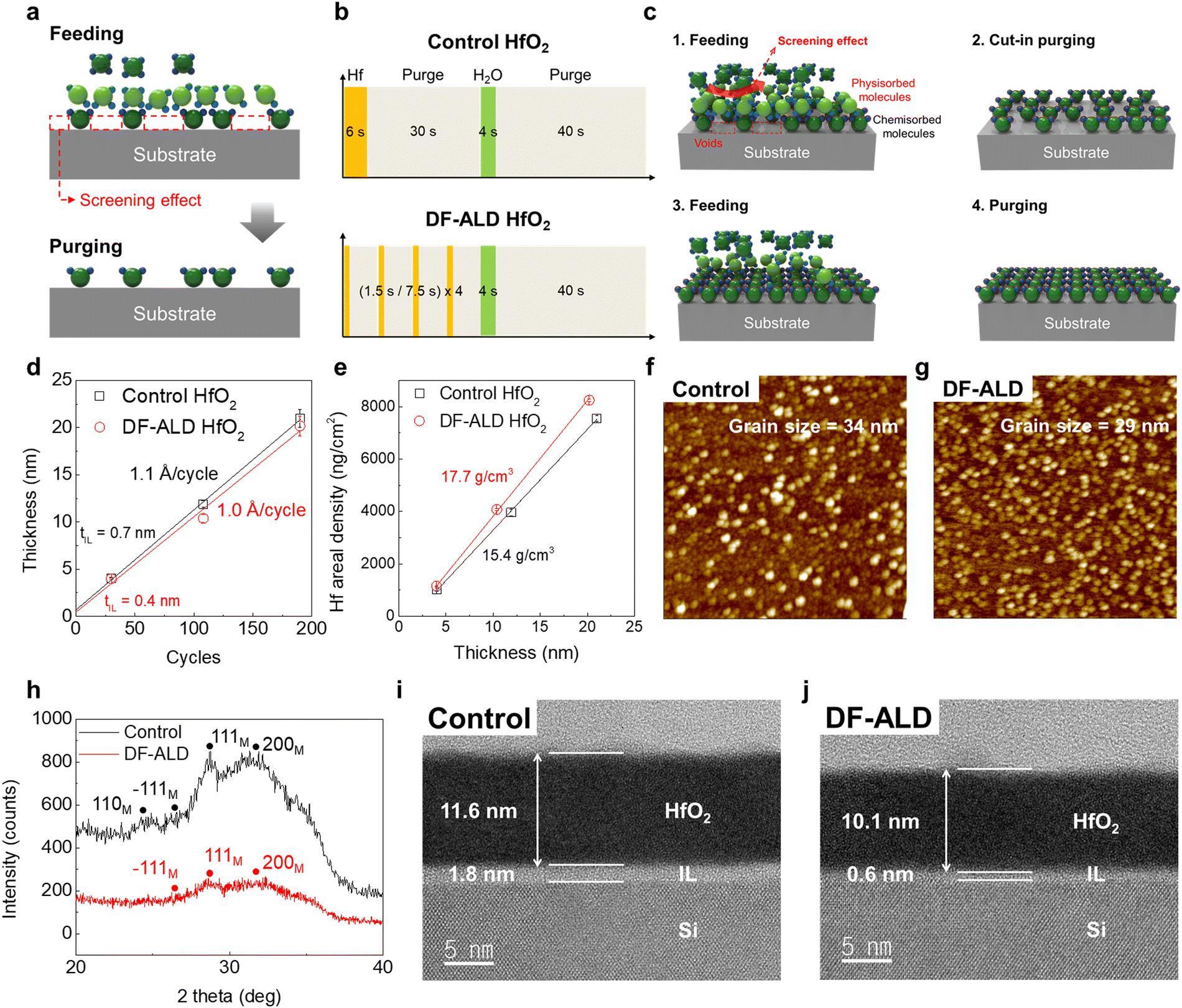 | ||
| Fig. 1 (a) Schematic diagram of the screening effect occurring due to the physisorbed precursor molecules. (b) Process sequence (recipe) and (c) schematic diagram of the DF-ALD process. (d) Comparison of HfO2 thickness between the control and DF-ALD process for different numbers of cycles; growth rates are 1.1 Å per cycle for control and 1.0 Å per cycle for DF-ALD, respectively. (e) Hf areal density measured using EDXRF dependent on HfO2 film thickness grown via the control and DF-ALD processes where the nominal density of the HfO2 film was calculated using the slope of the curves. AFM plan-view images for (f) control HfO2 and (g) DF-ALD HfO2 films. (h) GIXRD spectra (incident angle of 1°) for an ∼20 nm HfO2 thin film prepared by the control and DF-ALD processes. Cross-sectional HRTEM images of (i) the control HfO2 film and (j) the DF-ALD HfO2 film. | ||
The process sequence of the discrete feeding ALD (DF-ALD) involves supplying the precursor molecules separately a certain number of times without changing the total feeding/purging time (Fig. 1b). By employing the DF-ALD process, the factors screening the surface reactive groups, such as physisorbed precursor molecules or byproducts on the chemisorbed precursor molecules, can be efficiently eliminated, as depicted in Fig. 1c. Previously, similar trials have been conducted; Aria et al. and Muneshwar et al. suggested a process of repeated precursor feeding several times,3,8 and Wang et al. proposed a multiple short pulse process.9 However, the DF-ALD process employs a novel cut-in purge step which efficiently removes the physisorbed precursor molecules and byproducts, while the total process time is accurately maintained. More importantly, in this work, further detail of the mechanism is suggested and experimentally proven.
In this study, the DF-ALD process, which improves the growth behavior of thin films by increasing the surface adsorption efficiency of precursor molecules, was introduced into the HfO2 ALD process. Energy dispersive X-ray fluorescence (EDXRF), atomic force microscopy (AFM), and glancing incidence X-ray diffraction (GIXRD) confirmed the increase in nucleation density and physical film density of the DF-ALD film, and high-resolution transmission electron microscopy (HRTEM) results showed a significant decrease in the interfacial layer (IL) thickness. Auger electron spectroscopy (AES) and time-of-flight secondary ion mass spectrometry (ToF-SIMS) depth profile analysis revealed lower concentrations of impurities in the DF-ALD HfO2 film. As a result, various electrical properties of the DF-ALD film were also improved.
2. Experimental
2.1 ALD HfO2 thin films
Boron-doped p-type Si (100) substrates with a resistivity of ∼10 Ω cm were cleaned in a dilute hydrofluoric acid solution (∼10%) to eliminate the native oxide, and were rinsed in deionized water. HfO2 films with various thicknesses were grown on the cleaned Si wafer substrates in a 6-inch traveling wave-type thermal ALD reactor. High-purity N2 (99.999%) was used as a carrier and purge gas (200 sccm). The substrate temperature was maintained at 250 °C, which is within the temperature window for the ALD HfO2 process. Tetrakis(ethylmethylamido)hafnium (TEMAHf) and H2O were used as the Hf precursor and oxygen source, respectively. The feeding times of TEMAHf and H2O to accomplish the self-limited growth characteristics were 6 (Fig. S1a, ESI†) and 4 s, respectively. Under the sub-saturated conditions, the physical properties of the HfO2 film (growth rate, nominal density, and refractive index) were degraded (Fig. S1b–d, ESI†). The purging time after the TEMAHf and H2O exposures were 30 and 40 s, respectively.2.2 Physicochemical analysis
The HfO2 film thickness was measured using ex-situ spectroscopic ellipsometry (SE, MG-1000, Nano View Co.) with a spectral range of 380–900 nm at a fixed incidence light angle of 70°. The Hf layer density was measured by EDXRF (ARL Quant’X, Thermo Fisher Scientific Co.). The thickness, physical density, and roughness of the films were studied using X-ray reflectometry (XRR, ATX-G, Rigaku Co.). The crystallinity of films was estimated by XRD (Smartlab, Rigaku Co.) in the glancing incidence mode with a 1° incidence angle using Cu Kα radiation. The surface morphology of the films was investigated with AFM (XE-100, Park system) in tapping mode, and the root-mean-squared roughness values and grain sizes were extracted from the plan view AFM images. The microstructures of the HfO2 films were observed with an HRTEM (Libra 200 MC, Carl Zeiss) operating at 200 kV in the bright-field imaging mode. Samples for HRTEM imaging were prepared by focused ion beam (FIB, Quanta 3D FEG, FEI) sectioning. The chemical binding states of the films were evaluated with X-ray photoelectron spectroscopy (XPS, K-Alpha, Thermo Fisher Scientific Co.) using an Al Kα monochromatic source of 1486.6 eV. The binding energies of the XP spectra were calibrated with the Si 2p (Si–Si bonding, 99.6 eV) peak. The elemental depth profiles were performed by AES (PHI 700Xi, Physical Electronics) using an electron beam energy of 0.5 keV and ToF-SIMS (TOF·SIMS 5, ION-TOF) with a 30 keV Bi + ion gun (50 × 50 μm2).2.3 Electrical characterization
For electrical measurements, metal–oxide–semiconductor (MOS) capacitors were fabricated with 100 nm-thick TiN top electrodes deposited through a shadow mask via DC magnetron sputtering, which was followed by forming gas (5% H2, balanced with Ar) annealing at 400 °C for 30 min to reduce the interface state densities and improve the metal to dielectric contact. Then, an In–Ga eutectic alloy was used to form a backside ohmic contact. The capacitance–voltage (C–V) and current density–voltage (J–V) characteristics of the MOS devices were evaluated using a semiconductor parameter analyser system (4200-SCS, Keithley).3. Results and discussion
3.1 Growth behavior
For DF-ALD, the Hf precursor feeding step was divided into 4 steps as shown in Fig. 1b, which would remove the physisorbed excess precursor molecules or byproducts generated during the ALD reaction effectively and thus, the adsorption/filling efficiency of the precursor molecules on the substrate or film surface increased at the initial stage of ALD reaction (Fig. 1c). We confirmed that the process conditions hardly affected the total amount of precursor exposed in the control and DF-ALD processes (Fig. S2, ESI†). Fig. 1d shows the thickness of the control and DF-ALD HfO2 films as a function of the number of ALD cycles measured by SE. The linear thickness increase with the number of ALD cycles confirmed that the HfO2 thin films were grown in the typical ALD mode (self-limited surface reaction). The growth rate was 0.11 and 0.10 nm per cycle for the control and DF-ALD films, respectively. The IL thickness was evaluated with the y-intercept value obtained by interpolation, which was 0.70 and 0.44 nm for the control and DF-ALD films, respectively. The Hf layer density values measured by EDXRF as a function of the thickness of the control and the DF-ALD films are shown in Fig. 1e. The Hf layer density of the DF-ALD film is greater than that of the control film at the same film thickness, which suggests the higher physical density of the DF-ALD film. XRR confirmed the physical density of the film increased from 10.05 g cm−3 for the control film to 10.31 g cm−3 for DF-ALD HfO2 (Fig. S3, ESI†).Fig. 1f and g show AFM images and an average grain size of 20 nm-thick for the control and DF-ALD HfO2 films, respectively. The DF-ALD film exhibited a higher nucleation density and smaller grain size compared to the control film because the increased adsorption efficiency of Hf precursor molecules during DF-ALD induced a larger number of nuclei on the substrate. The difference in nucleation behavior was reflected in the crystallinity of the films. GIXRD patterns of the 20 nm-thick films in Fig. 1h show that the degree of crystallinity decreased in the DF-ALD HfO2 film, which coincided with the AFM results in terms of decreased grain size. The microstructure of the HfO2 films was observed using cross-sectional HRTEM analysis as shown in Fig. 1i and j. Most notably, the thickness of IL between the HfO2 layer and the Si substrate was significantly thinner for the DF-ALD film (∼0.6 nm), ∼30% of that for control ALD film (∼1.8 nm). This is because an increased surface coverage of precursor molecules during a feeding step at the initial stage of DF-ALD suppressed the surface oxidation of the Si substrate by the oxygen source, H2O pulse.10–13
3.2 Chemical structure
The chemical binding states of the films (∼4 nm) was examined with XPS analysis as shown in Fig. 2a–c. There was no significant difference between the control and DF-ALD HfO2 films in the Hf 4f core level spectrum, which indicates that the chemical structures of the HfO2 upper layers in both films are almost identical. However, the Si 2p and O 1s core level spectra show a clear difference between the two films. The peaks for Si–O bonding (SiOx) at the binding energy of 102.3 eV and 532.3 eV in Si 2p and O 1s core level spectra, respectively,14–16 originate from the IL, which are significantly suppressed in the DF-ALD film compared to the control ALD film. This is consistent with the HRTEM results (Fig. 1j). An AES depth profile was carried out to observe the distribution of the elemental composition in the films as shown in Fig. 2d and e. The Hf and O were uniformly distributed throughout the film, and the C impurity concentration was half the value in the DF-ALD film (2.5%) than in the control ALD film (5%). This was confirmed by a ToF-SIMS depth profile analysis in Fig. 2f. The signal intensities of C and C–N, major residual impurities originating from the Hf precursor, were lower in the DF-ALD film than in control ALD film, and in particular, the C–N signal intensity significantly decreased by an order of magnitude in the DF-ALD film. This is attributed to the ‘cooperative effect’ in the surface chemical reaction;17–19 the number of chemically-adsorbed precursor molecules on the substrate or film surface increased in DF-ALD, which enhanced the ALD reaction leaving less residual impurities in the film. This in turn increased the physical density of the DF-ALD HfO2 films.20–22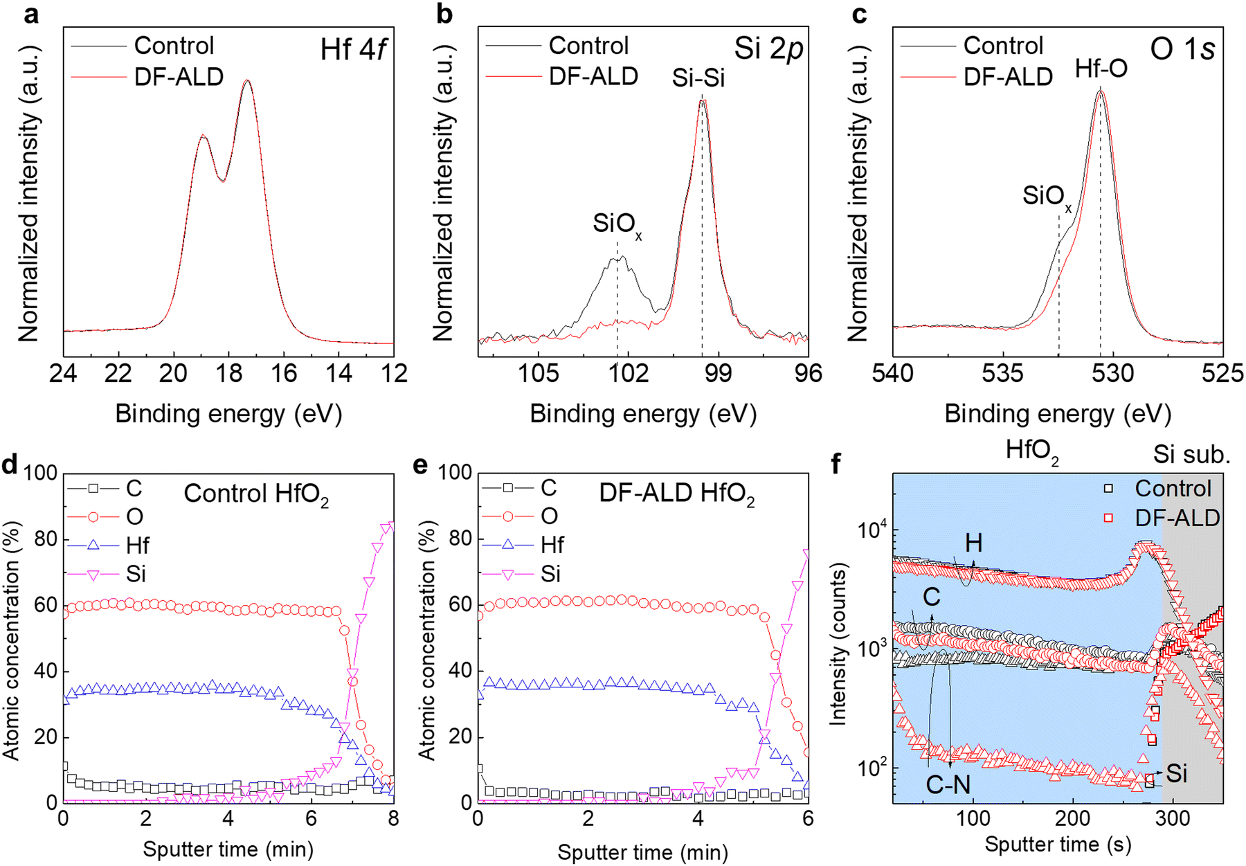 | ||
| Fig. 2 (a) Hf 4f, (b) Si 2p, and (c) and O 1s core level XPS spectra of HfO2 films grown via the control and DF-ALD processes. AES depth profiles of Hf, O, Si, C and N of the (d) control and (e) DF-ALD HfO2 films. (f) ToF-SIMS depth profiles of H, C and C–N in the control HfO2 and DF-ALD HfO2 thin films. | ||
3.3 Electrical properties
To verify the effects of the DF-ALD on the electrical properties of the films, MOS capacitors were fabricated with 4 and 20 nm thick control and DF-ALD HfO2 films, and the C–V characteristics were examined as shown in Fig. 3a. The hysteresis values were smaller for the DF-ALD films compared to those with the control ALD films, because the number of charge trapping sites such as border and bulk traps/defects originating from the impurities were reduced by DF-ALD. Fig. 3b shows the capacitance equivalent thickness (CET) obtained from the capacitance density of each HfO2 film in Fig. 3a as a function of the physical thickness. The dielectric constants calculated based on the slope of curves for the DF-ALD film is ∼16, higher than ∼14 for the control film, which is attributed to the increased film density and the reduced impurity concentration of the DF-ALD HfO2 film as discussed above.23–25 In addition, the CET of the IL (CETIL) evaluated from the y-intercept of the curves is lower for the DF-ALD film (∼0.06 nm), and is one-third of the control film (∼0.17 nm), which is consistent with the HRTEM results (Fig. 1i and j). The calculated fixed charge density (Qf) in each HfO2 film showed a similar level of ∼4.3 × 10¹² and ∼4.6 × 1012 cm−2 for the control and DF-ALD films, respectively. The interface state densities (Dit) of a number of 20 nm-thick HfO2 samples were measured using the conductance method,26,27 as shown in Fig. 3c. The Dit of the control HfO2 film varied widely over two orders of magnitude, whereas the DF-ALD film exhibited decreased Dit in the overall band region, and the variation was significantly reduced. This implied that the DF-ALD improved HfO2/Si interface characteristics for the aforementioned reasons.28–30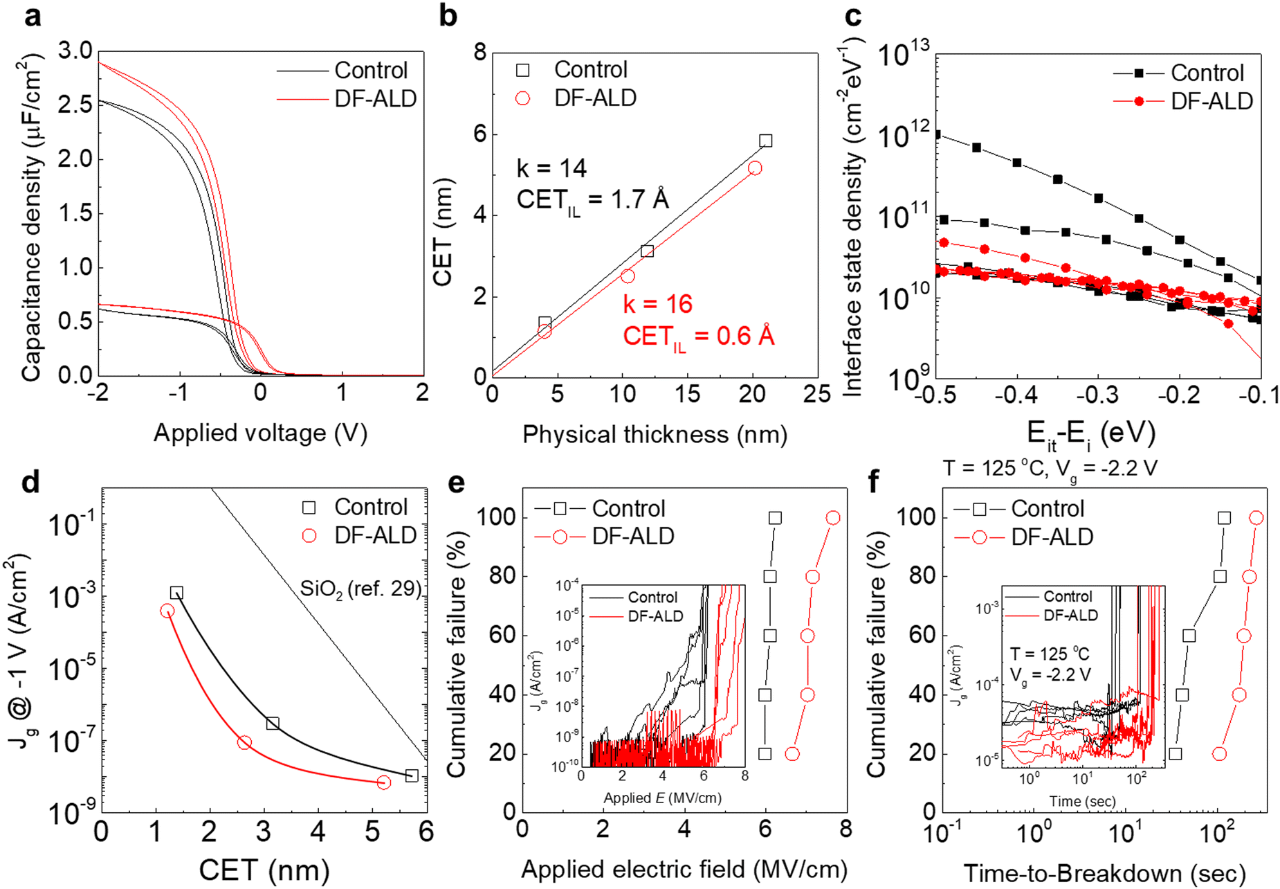 | ||
| Fig. 3 (a) Typical capacitance–voltage plots for ∼4 nm and ∼20 nm HfO2 films grown via the control and DF-ALD processes, respectively. (b) Plot of physical thickness vs. CET for the control HfO2 and DF-ALD HfO2 films. (c) Interface state density (Dit) measured for ∼20 nm of HfO2 films using conductance method. (d) Variation of Jg for both the control and DF-ALD HfO2 films as a function of CET. (e) Cumulative distribution plots of TZDB and (f) TDDB. TDDB was measured under constant voltage stress of −2.2 V at T = 125 °C (Insets: raw J–E and J–time curve for TZDB and TDDB). | ||
Fig. 3d shows the plot of CET vs. leakage current density (Jg) of the MOS capacitors to examine the insulating characteristics of the HfO2 films. The Jg for the DF-ALD HfO2 film is lower by about an order of magnitude compared to the control film. The simulation results of the SiO2 film were also included for comparison.31 The device reliabilities such as the time–zero dielectric breakdown (TZDB) and the time-dependent breakdown (TDDB) characteristics were also examined and their cumulative failure results are shown in Fig. 3e and f, respectively. The Jg–E and Jg–time curves are also included as inset figures. The average breakdown field is higher for the DF-ALD HfO2 film (∼7.1 MV cm−1) than the control HfO2 film (∼6 MV cm−1) (Fig. 3e). For the TDDB characteristics, a constant voltage was applied to the devices at a high temperature of 125 °C, and the average time-to-breakdown for the DF-ALD HfO2 film (∼192 s) is more than twice as long as the control film (∼70 s) (Fig. 3f). The improvements in the electrical characteristics in the DF-ALD film are attributed to the increased film density and the reduced impurity concentration in the film as discussed above.32–34
4. Conclusions
In summary, we demonstrate improvements in physicochemical and electrical properties of the ALD HfO2 film grown with a discrete feeding method, which provides a full saturated surface coverage of precursor molecules maintaining total feeding time. This is because the “screening effect” was overcome; The physisorbed precursor molecules or byproducts on the chemisorbed precursor molecules could be effectively eliminated, resulting in an improved adsorption efficiency and surface filling rate of the precursor molecules. As a result, DF-ALD increased the HfO2 film density, reduced the IL thickness and reduced impurities in the film. Assorted electrical properties of the film such as permittivity, bulk/border trap density, interface state density, gate leakage current and breakdown characteristics were also improved. DF-ALD could be applied to more diverse ALD processes due to its easy-to-apply characteristics.Author contributions
J. C. P. conceived the study, carried out the experiments. C. I. C. contributed to the characterization of samples. S.-G. L., S. J. Y., J. H. L. and J. H. J. prepared the TEM samples and conducted the microstructure analysis. W.-H. K., J.-H. A., J. H. K. and T. J. P. wrote manuscript and contributed to revising the manuscript. T. J. P. conceived the original ideas and supervised the project. All authors contributed to the manuscript and have given approval of the final version of the manuscript.Conflicts of interest
There are no conflicts of interest to declare.Acknowledgements
This work was supported by the Materials and Components Technology Development Program (20010275 and 20010727) funded by the Ministry of Trade, Industry & Energy (MOTIE, Republic of Korea).References
- S. M. George, Chem. Rev., 2010, 110, 111–131 CrossRef CAS PubMed.
- R. L. Puurunen, Chem. Vap. Deposition, 2003, 9, 249–257 CrossRef CAS.
- T. Muneshwar and K. Cadien, J. Appl. Phys., 2016, 119, 085306 CrossRef.
- T. Muneshwar and K. Cadien, J. Appl. Phys., 2018, 124, 095302 CrossRef.
- T. J. Park, J. H. Kim, J. H. Jang, U. K. Kim, S. Y. Lee, J. Lee, H. S. Jung and C. S. Hwang, Chem. Mater., 2011, 23, 1654–1658 CrossRef CAS.
- J. W. Han, H. S. Jin, Y. J. Kim, J. S. Heo, W.-H. Kim, J.-H. Ahn, J. H. Kim and T. J. Park, Nano Lett., 2022, 22(11), 4589–4595 CrossRef PubMed.
- J.-M. Lee, J. Lee, J. W. Han, H. Park, S. Kyung, I. W. Kim, J. M. Lee, T. J. Park and W.-H. Kim, Appl. Surf. Sci., 2021, 539, 148247 CrossRef CAS.
- A. I. Aria, K. Nakanishi, L. Xiao, P. Braeuninger-Weimer, A. A. Sagade, J. A. Alexander-Webber and S. Hofmann, ACS Appl. Mater. Interfaces, 2016, 8, 30564–30575 CrossRef CAS PubMed.
- H. Wang, Z. Wang, X. Xu, Y. Liu, C. Chen, P. Chen, W. Hu and Y. Duan, Appl. Phys. Lett., 2019, 114, 201902 CrossRef.
- M. Xu, C. Zhang, S.-J. Ding, H.-L. Lu, W. Chen, Q.-Q. Sun, D. W. Zhang and L.-K. Wang, J. Appl. Phys., 2006, 100, 106101 CrossRef.
- G. P. Gakis, C. Vahlas, H. Vergnes, S. Dourdain, Y. Tison, H. Martinez, J. Bour, D. Ruch, A. G. Boudouvis and B. Caussat, Appl. Surf. Sci., 2019, 492, 245–254 CrossRef CAS.
- R. De Almeida and I. J. R. Baumvol, Surf. Sci. Rep., 2003, 49, 1–114 CrossRef CAS.
- M. Cho, J. Park, H. B. Park, C. S. Hwang, J. Jeong and K. S. Hyun, Appl. Phys. Lett., 2002, 81, 334–336 CrossRef CAS.
- Y. Won, S. Park, J. Koo, S. Kim, J. Kim and H. Jeon, Appl. Phys. Lett., 2005, 87, 262901 CrossRef.
- R. Jiang, E. Xie and Z. Wang, Appl. Phys. Lett., 2006, 89, 142907 CrossRef.
- J.-C. Lee, S.-J. Oh, M. Cho, C. S. Hwang and R. Jung, Appl. Phys. Lett., 2004, 84, 1305–1307 CrossRef CAS.
- M. Shirazi and S. D. Elliott, Nanoscale, 2015, 7, 6311–6318 RSC.
- Y. Maimaiti and S. D. Elliott, Chem. Mater., 2016, 28, 6282–6295 CrossRef CAS.
- S. D. Elliott, G. Dey, Y. Maimaiti, H. Ablat, E. A. Filatova and G. N. Fomengia, Adv. Mater., 2016, 28, 5367–5380 CrossRef CAS PubMed.
- D. Triyoso, R. Liu, D. Roan, M. Ramon, N. Edwards, R. Gregory, D. Werho, J. Kulik, G. Tam and E. Irwin, J. Electrochem. Soc., 2004, 151, F220 CrossRef CAS.
- R. L. Puurunen, A. Delabie, S. Van Elshocht, M. Caymax, M. L. Green, B. Brijs, O. Richard, H. Bender, T. Conard and I. Hoflijk, Appl. Phys. Lett., 2005, 86, 073116 CrossRef.
- K.-M. Kim, J. S. Jang, S.-G. Yoon, J.-Y. Yun and N.-K. Chung, Materials, 2020, 13, 2008 CrossRef CAS PubMed.
- J. H. Kim, T. J. Park, S. K. Kim, D.-Y. Cho, H.-S. Jung, S. Y. Lee and C. S. Hwang, Appl. Surf. Sci., 2014, 292, 852–856 CrossRef CAS.
- S. K. Kim, S. W. Lee, C. S. Hwang, Y.-S. Min, J. Y. Won and J. Jeong, J. Electrochem. Soc., 2006, 153, F69 CrossRef CAS.
- S. W. Lee, O. S. Kwon, J. H. Han and C. S. Hwang, Appl. Phys. Lett., 2008, 92, 222903 CrossRef.
- T. Hori, Gate dielectrics and MOS ULSIs: principles, technologies and applications, Springer Science & Business Media, 2012 Search PubMed.
- H. Yang, Y. Son, S. Choi and H. Hwang, Jpn. J. Appl. Phys., 2005, 44, L1460 CrossRef CAS.
- S. Jeon and S. Park, Microelectron. Eng., 2011, 88, 872–876 CrossRef CAS.
- C. Liao, X. Zou, C.-W. Huang, J. Wang, K. Zhang, Y. Kong, T. Chen, W.-W. Wu, X. Xiao and C. Jiang, IEEE Electron Device Lett., 2015, 36, 1284–1286 CAS.
- B. Ren, M. Liao, M. Sumiya, J. Su, X. Liu, Y. Koide and L. Sang, J. Phys. D: Appl. Phys., 2018, 52, 085105 CrossRef.
- Y.-C. Yeo, T.-J. King and C. Hu, Appl. Phys. Lett., 2002, 81, 2091–2093 CrossRef CAS.
- M. Seo, Y.-S. Min, S. K. Kim, T. J. Park, J. H. Kim, K. D. Na and C. S. Hwang, J. Mater. Chem., 2008, 18, 4324–4331 RSC.
- J. W. Lim and S. J. Yun, Electrochem. Solid-State Lett., 2004, 7, F45 CrossRef CAS.
- H. Kim, S. Woo, J. Lee, Y. Kim, H. Lee, I.-J. Choi, Y.-D. Kim, C.-W. Chung and H. Jeon, J. Electrochem. Soc., 2010, 158, H21 CrossRef.
Footnote |
| † Electronic supplementary information (ESI) available. See DOI: https://doi.org/10.1039/d2tc03485a |
| This journal is © The Royal Society of Chemistry 2023 |