
Electrodeposited NaYF4:Yb3+, Er3+ up-conversion films for flexible neural device construction and near-infrared optogenetics†
Xuran
Zhang‡
abc,
Jianfei
Ding
a,
Liang
Zou
abc,
Huihui
Tian
a,
Ying
Fang
 *abcd and
Jinfen
Wang‡
*a
*abcd and
Jinfen
Wang‡
*a
aCAS Center for Excellence in Nanoscience, National Center for Nanoscience and Technology, Beijing, 100190, China. E-mail: wangjinfen@nanoctr.cn; fangy@nanoctr.cn
bCAS Center for Excellence in Brain Science and Intelligence Technology, Institute of Neuroscience, Chinese Academy of Sciences, Shanghai, 200031, China
cUniversity of Chinese Academy of Sciences, Beijing, 100049, China
dChinese Institute for Brain Research, Beijing, 102206, China
First published on 20th March 2023
Abstract
Near-infrared optogenetics based on up-conversion materials provides a promising tool for the dissection of neural circuit functions in deep brain regions. However, it remains a challenge to combine near-infrared up-conversion optogenetic stimulation with high-density electrophysiological recording in a minimally invasive manner. Here, we develop a flexible device for simultaneous electrophysiological recording and near-infrared optogenetics. The flexible device is constructed by integrating polymer-based flexible recording microelectrodes with electrodeposited NaYF4:Yb3+, Er3+ up-conversion films that can convert deep-tissue-penetrating near-infrared light into visible light for optogenetic activation of C1V1-expressing neurons. The emission properties of the up-conversion films are optimized for green light emission to stimulate C1V1 opsins. Owing to their minimized surgical footprint and high mechanical compliance, chronically implanted devices enable simultaneous electrophysiological recording and near-infrared optogenetic modulation of neuronal activities in the brain.
10th Anniversary StatementThe brain is the most complex organ in the body. New technologies for neural activity recording and modulation in vivo are critical for the dissection of neural circuit mechanisms underlying behaviors. In the past ten years, Journal of Materials Chemistry B has endeavored to study the neural interfaces and devices based on novel materials. In this manuscript, we demonstrate a flexible neural device based on up-conversion materials for simultaneous recording and manipulating neural activities. Because of the low invasiveness and good biocompatibility of the flexible up-conversion device, it can allow for long-term electrophysiological recording and near-infrared optogenetics in the brain. We foresee that biocompatible, ultraflexible, and multifunctional neural devices will open up new opportunities in both basic and applied neuroscience. |
Introduction
Optogenetics employs light to selectively control the activity of cells that are genetically engineered with light-gated channels, i.e. opsins, and has significantly improved our understanding of neural circuit functions.1–5 Most transmembrane opsins respond to visible light (400–700 nm). For example, C1V1 is a channel rhodopsin variant that can be activated by green light with a strong photocurrent. However, visible light has limited penetration depth in the brain tissue because of high absorption and scattering by biological tissue, which makes it necessary to implant an optical fiber into the targeted brain tissues for the delivery of visible light. The implantation of the optical fiber can lead to both acute and chronic tissue damages in the brain. On the other hand, near-infrared (NIR) light has deeper tissue penetration capability compared to visible light.6 Recently, up-conversion (UC) materials that can convert NIR light into visible light have attracted significant attention for minimally invasive optogenetics, especially in deep brain regions.7–10UC-mediated NIR optogenetics typically relies on the syringe injection of up-conversion nanoparticles (UCNPs) into targeted brain regions.11–13 After injection, UCNPs can convert deep-tissue-penetrating NIR light into visible light to control the activity of nearby opsin-expressing cells. Recording microelectrodes can be implanted into the same brain regions for simultaneous optogenetic stimulation and electrophysiological recordings. However, UCNPs have low diffusion capability in the brain tissue,11,14 making it extremely challenging to spatially co-localize the recording microelectrodes with UCNPs. In addition, traditional microelectrode probes are usually based on rigid materials, such as silicon and metal, resulting in a significant mechanical mismatch between rigid probes and soft brain tissues.15–18 The mechanical mismatch between the probes and tissues has been shown to induce chronic inflammatory responses, resulting in glial scar formation and signal degradation over the long term.19–22 Thus, it is highly desirable to develop flexible devices that can enable simultaneous optogenetic stimulation and electrophysiological recording in a minimally invasive manner.
Lanthanide-doped sodium yttrium fluoride (NaYF4:Ln3+) represents one of the most applied UC materials because of its high UC efficiency and tunable emission wavelength. NaYF4:Ln3+ is typically prepared through solid-state reactions to form bulk materials, or through solution chemistry routes to form nanoparticles.23–27 However, bulk NaYF4:Ln3+ materials are usually synthesized at a high temperature of 1000 °C in a HF gas atmosphere, which is incompatible with the microfabrication process of flexible microelectrodes. NaYF4:Ln3+ nanoparticles are promising for biological applications because of their mild preparation, small sizes, and high UC efficiency.28–32 However, to construct flexible devices, NaYF4:Ln3+ nanoparticles have to be assembled or embedded in a polymer matrix, which presents a technical challenge during microfabrication and also might lead to reduced UC efficiency.8,33 On the other hand, electrodeposition offers a simple and controllable route to prepare thin up-conversion films with good adhesion on both planar and curved substrates.34,35 In this work, we developed a flexible neural device by integrating polymer-based microelectrodes with electrodeposited NaYF4:Yb3+, Er3+ UC films. The NIR-to-green light conversion of the electrodeposited NaYF4:Yb3+, Er3+ UC films was optimized through chemical composition and crystalline phase engineering. The polymer-based microelectrodes could form stable interfaces with tissues for neuronal activity recordings, whereas the electrodeposited UC films could convert NIR light to green light for optogenetic stimulation of C1V1-expressing neurons in mouse brain. As a result, chronically implanted flexible neural devices enabled simultaneous NIR optical stimulation and electrophysiological recording in the brain over several weeks.
Experimental
Materials
Yttrium nitrate hexahydrate (Y(NO3)3·6H2O, 99.8%), ytterbium nitrate pentahydrate (Yb(NO3)3·5H2O, 99.9%), erbium nitrate pentahydrate (Er(NO3)3·5H2O, 99.9%), ethylene-diaminetetraacetic acid disodium salt dehydrate (EDTA-2Na·2H2O, ≥99.0%), sodium ascorbate (C6H7O6Na, ≥99.0%), ammonium fluoride (NH4F, ≥98.0%) were purchased from Sigma-Aldrich Chemical Reagent Co., Ltd. Iron chloride hexahydrate (FeCl3·6H2O, 99%) was purchased from Aladdin Ltd (Shanghai, China). Ammonium hydroxide solution (NH3·H2O, 25–28%) and chloroplatinic acid hydrate (H2Cl6Pt·xH2O, 99.995%) were purchased from Macklin Ltd (Shanghai, China). Glacial acetic acid (CH3COOH, ≥99.5%) was purchased from Modern Oriental Fine Chemistry Ltd (Beijing, China). Paraformaldehyde ((CH2O)n, 4%) was purchased from Biosharp Life Science (Hefei, China). All these reagents were used as received. The indium tin oxide (ITO) coated glass substrate (sheet resistance: 7–10 Ω) was purchased from GuLuo Glass Ltd (Luoyang, China).Electrodeposition of NaYF4:Yb3+, Er3+ thin film
10 mL 0.1 mol L−1 EDTA-2Na solution and 10 mL 0.1 mol L−1 rare earth nitrate solution with a molar ratio of Y3+![[thin space (1/6-em)]](https://www.rsc.org/images/entities/char_2009.gif) : Yb3+:Er3+ = 78:20:2 were mixed under magnetic stirring until the solution turned turbid. The pH of the mixed solution was then adjusted to 8 with 3.5 mol L−1 NH3·H2O solution. 10 mL NH4F solution with concentrations ranging from 1 to 4 mol L−1 was added dropwise to the solution and then 10 mL 0.5 mol L−1 sodium ascorbate solution was added to the solution. After adjusting the pH to 6.3 with 0.5 mol L−1 HNO3, a clear electrodeposition solution was obtained. The electrodeposition solution was freshly prepared before electrodeposition process to avoid sodium ascorbate oxidation.
: Yb3+:Er3+ = 78:20:2 were mixed under magnetic stirring until the solution turned turbid. The pH of the mixed solution was then adjusted to 8 with 3.5 mol L−1 NH3·H2O solution. 10 mL NH4F solution with concentrations ranging from 1 to 4 mol L−1 was added dropwise to the solution and then 10 mL 0.5 mol L−1 sodium ascorbate solution was added to the solution. After adjusting the pH to 6.3 with 0.5 mol L−1 HNO3, a clear electrodeposition solution was obtained. The electrodeposition solution was freshly prepared before electrodeposition process to avoid sodium ascorbate oxidation.
The electrodeposition of NaYF4:Yb3+, Er3+ film on the conductive substrates was performed on a CHI660E electrochemical station (CH Instruments, Shanghai, China). An ITO coated glass substrate, graphite electrode and Ag/AgCl electrode were utilized as the working electrode, counter electrode and reference electrode, respectively. The NaYF4:Yb3+, Er3+ film was deposited for 1800 s with a voltage of 1.2 V (vs. Ag/AgCl) at the temperature of 65 °C. As-prepared films were cleaned in glacial acetic acid and then annealed at 300 °C for 2 hours in air.
NaYF4:Yb3+, Er3+ thin film characterizations
The morphology of NaYF4:Yb3+, Er3+ films was characterized by scanning electron microscopy (SEM, S4800, Hitachi, Tokyo, Japan). X-Ray diffraction (XRD, D/MAX-TTRIII (CBO) diffractometer, Saitama, Japan) with Cu Kα radiation (λ = 1.5418 Å) was used to determine the crystal structure. X-Ray photoelectron spectroscopy (XPS, ESCALAB250Xi, Thermo Fisher Scientific, Waltham, MA) was performed to analyze the elemental composition of the thin films. The UC fluorescence of the thin films were measured on a fluorescence spectrophotometer (NanoLOG-TCSPC, HORIBA Jobin Yvon, Paris, France) using a 980 nm laser diode as the excitation source. All measurements were performed at room temperature.Fabrication of flexible microelectrode arrays
Flexible microelectrode arrays were fabricated using standard microfabrication processes (Fig. S1, ESI†). Main fabrication steps were as follows: (1) A sacrificial layer was constructed on a silicon wafer (Silicon Valley Microelectronics Inc., Santa Clara, CA) by magnetron sputtering (Lab 18, Kurt J. Lesker Ltd, Frankfurt am Main, Germany) of 100 nm-thick aluminum. (2) The bottom insulating layer was formed by spin-coating of 1 μm-thick layer of polyimide (PI, U-Varnish S, UBE Industries, Ltd, Tokyo, Japan) and then cured at 200 °C for 2 hours under vacuum. (3) The wafer was spin-coated with Shipley S1813 positive photoresist (Microposit, the Dow Chemical Company, Midland, MI) and baked at 115 °C for 3 min. The photoresist layer was patterned using photolithography (MA6 Mask Aligner, SUSS MicroTec Group, Garching, Germany) and then developed in MF 319 (Microposit, the Dow Chemical Company). (4) 5 nm-thick layer of chromium and 100 nm-thick layer of gold were deposited on the wafer to form the recording sites, interconnections, and bonding pads. (5) Step 2 was repeated to form the middle 1 μm-thick PI layer. (6) Step 3 and 4 was repeated to form the interconnection lines for the electrodeposition of the NaYF4:Yb3+, Er3+ film. The NaYF4:Yb3+, Er3+ film was electrodeposited for 300 s at 1.2 V and 65 °C. The concentrations of reactants in the electrolyte solution were as follows: 0.2 to 0.8 mol L−1 F−, 0.14 mol L−1 Na+, 0.1 mol L−1 ascorbate anions, 0.02 mol L−1 EDTA, 0.0156 mol L−1 Y3+, 0.004 mol L−1 Yb3+, 0.0004 mol L−1 Er3+. (7) Step 2 was repeated to form the top 1 μm-thick PI layer. (8) The wafer was spin-coated with a AZ4620 positive photoresist (Hoechst Celanese Corp., Irving, TX) and patterned by photolithography. Then RIE (etching conditions: 20 sccm O2, 200 W, 20 Pa) was performed to remove the exposed PI to form the filament structure and expose recording sites and bonding pads. (9) The Al sacrificial layer was removed with 1 mol L−1 FeCl3 solution to release the flexible devices from the wafer. (10) Nano-platinum or PEDOT was electrodeposited on the recording sites using a Gamry Reference 3000 electrochemical workstation (Gamry Instruments, Warminster, PA). The microelectrode, platinum electrode, and Ag/AgCl electrode were utilized as the working electrode, counter electrode, and reference electrode, respectively. The electrodeposition of poly(3,4-ethlenedioxythiophene)–poly (styrene sulfonate) (PEDOT: PSS) was performed in an aqueous solution with 0.14% w/v PEDOT and 0.05% w/v PSS. The electrodeposition current was 10 μA.Assembly of implantable flexible neural devices
A flexible microelectrode array and an optical fiber (Plexon Inc., Dallas, TX) were aligned together with a homemade 3D printed holder. The distance between the tips of the probe and optical fiber was ca. 2.5–3 mm. The device was withdrawn from 100 °C polyethylene glycol (PEG) bath, during which, the flexible probe filaments spontaneously assembled on the optical fiber surface under the capillary force of the molten PEG.Device structure characterizations
Optical images of the fabricated devices and the assembled devices were carried out using an Olympus BX51 microscope (Tokyo, Japan). SEM images of the devices were obtained on a Hitachi S4800. The surface roughness of the flexible UC devices was measured using an atomic force microscope (AFM, Multimode-8, Bruker, Billerica, MA). The fluorescence emission of the assembled devices was characterized using an optical fiber equipped with a 980 nm laser diode as the excitation source. The fluorescence images were collected by using a 600 nm low-pass filter.Animal and surgery
All procedures were performed in accordance with Animal Care and Use Committee of the National Center for Nanoscience and Technology, China. Male C57BL6/N mice aged between 6 and 8 weeks (Vital River Laboratory Animal Technology Ltd, Beijing, China) were used for the experiments. The mice were kept in a 12 h:12 h light:dark cycle with ad libitum access to food and water.
Mice were anesthetized by intraperitoneal injection of avertin (0.1 mL g−1, AIBI Biotech Ltd, Nanjing, China). The body temperature of the animal was maintained to 37 °C by an electric blanket, and the eyes were smeared with hydrochloride eye ointment (Shuangji Pharmaceutical Ltd, Beijing, China). A mouse was head-fixed on a stereotaxic frame (RWD Life Science Ltd, Shenzhen, China). A homemade stainless steel plate with a ground wire was glued to the skull of the mouse. 300 nL AAV9-hSyn::C1V1-mCherry was injected into the M2/VO brain region (anteroposterior, +2.50 mm; mediolateral, +0.50 mm; dorsoventral, −0.80, −1.40 and −2.00 mm, respectively). The injection rate was 100 nL min−1 and controlled by a PUMP 11 ELITE Nanomite (Harvard apparatus, Inc., Holliston, MA). The syringe was left in the brain for 5 minutes after each injection to avoid reflux. A flexible neural device was implanted into the same location at a depth of 2–3 mm. Dental cement (Shanghai New Century Dental Materials, Shanghai, China) was used to secure the device. Antibiotics were intraperitoneally injected within 3 days after surgery.
NIR optogenetics and neural activity recordings
All optogenetic experiments were performed on head-fixed, awake mice three weeks after AAV9-hSyn::C1V1-mCherry injection. Light illumination was delivered to the brain surface by suing the optical fiber that was equipped using a diode laser (Newdoon Technology Ltd, Hangzhou, China). 980 nm NIR light was delivered in a square wave pattern with power density from 4.78 to 14.33 W mm−2. A 128-channel recording system (Blackrock Microsystems, LLC, Salt Lake City, UT, Central application version 7.0.16.) was used to record the electrophysiological signals at a sampling rate of 30 kHz. The analysis of action potential data was performed by using Offline Sorter software (Plexon, Dallas, TX, Offline Sorter application version 4.4.0). The data were filtered between 250 and 5000 Hz, and common average referencing was applied to eliminate noise and light artifacts. The threshold of waveform detection was −4.5σ, where σ was the standard deviation from mean of peak heights histogram. Detected waveforms were further sorted into clusters using principal component analysis. Clusters with isolation distances above 15 were further analyzed.Results and discussion
Electrodeposition of NaYF4:Yb3+, Er3+ UC thin films
In our study, NaYF4:Yb3+, Er3+ thin films were electrodeposited on a conductive substrate, such as indium tin oxide (ITO) or gold film, through the following reactions (Fig. 1a):| R3+ + EDTA → R3+ − EDTA | (1) |
| C6H7O6− → C6H6O6 + H+ + 2e− | (2) |
| R3+ − EDTA + xH+ → HxEDTAx−3 + R3+ | (3) |
| R3+ + Na+ + 4F− → NaRF4↓ | (4) |
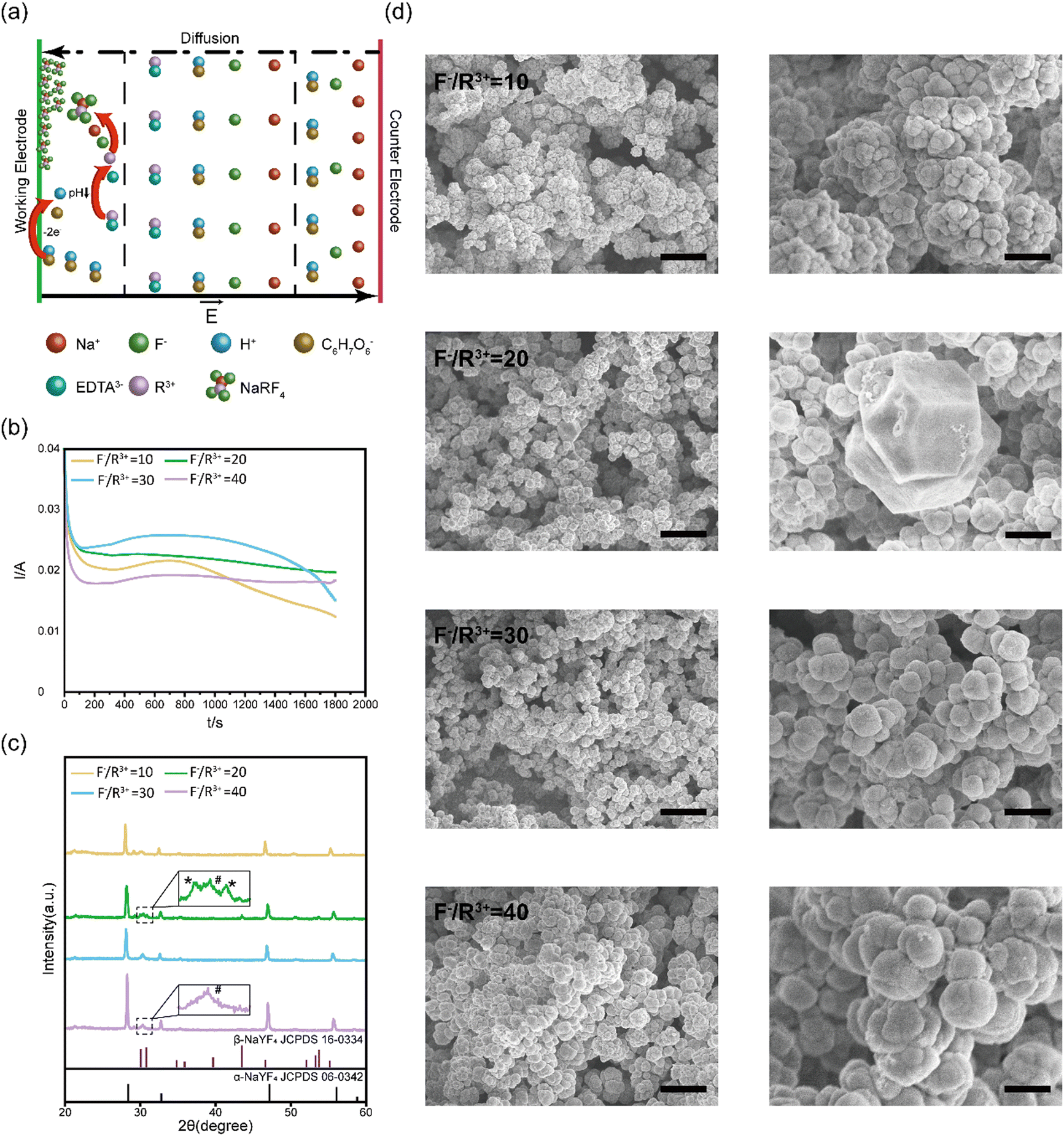 | ||
| Fig. 1 Electrodeposition of NaYF4:Yb3+, Er3+ thin films. (a) Schematic of the formation process of NaYF4:Yb3+, Er3+ thin films. (b) Electrodeposition curves at different F−/R3+ ratios on the ITO substrate at 1.2 V. (c) XRD of NaYF4:Yb3+, Er3+ thin films formed at different F−/R3+ ratios. Inset shows the magnified view near 30°, where * and # indicate peaks of β-NaYF4 and ITO, respectively. (d) SEM images of NaYF4:Yb3+, Er3+ thin films on the ITO substrate at different F−/R3+ ratios. Scale bars: 4 μm (left) and 1 μm (right). | ||
We systematically characterized the formation kinetics, crystalline structures, and microscale morphologies of electrodeposited NaYF4:Yb3+, Er3+ thin films prepared at different ratios of F− and R3+. The electrodeposition curves on the ITO substrates at different F−/R3+ ratios are summarized in Fig. 1b. The electrodeposition current stabilized around 20–30 mA. During this period, the pH value of the solution gradually decreased to 4.5, and released R3+ ions reacted with F− and Na+ ions to form NaYF4:Yb3+, Er3+ thin films. With the formation of the insulating NaYF4:Yb3+, Er3+ films on the conductive substrate, the amplitude of the electrodeposition currents started to decrease because the insulating films blocked the electron transfer between ascorbate anions and conductive substrate.
After electrodeposition, the NaYF4:Yb3+, Er3+ thin films were annealed at 300 °C for 2 hours for crystallization. The structure of the annealed NaYF4:Yb3+, Er3+ thin films deposited at different F−/R3+ ratios were characterized with XRD. As shown in Fig. 1c, the XRD diffraction peaks of the films are sharp, indicating the high crystallization of the annealed NaYF4:Yb3+, Er3+ thin films. At an F−/R3+ ratio of 10, there were three XRD peaks at 28.401°, 47.149°, and 56.065°, which correspond to the (111), (220), and (311) crystal planes of cubic-phase NaYF4 (α-NaYF4, JCPDS card no. 06-0342), respectively. When the F−/R3+ ratio was increased to 20, new XRD diffraction peaks appeared at 30.785°, 43.494°, 53.277°, and 53.75°, which can be indexed to the (101), (201), (300), and (211) crystal planes of hexagonal-phase NaYF4 (β-NaYF4, JCPDS card no. 16-0334). The XRD results showed that the electrodeposited thin films at an F−/R3+ ratio of 20 were a mixture of α-NaYF4 and β-NaYF4. When the F−/R3+ ratio was further increased to 30 and 40, the crystal structure of the electrodeposited NaYF4:Yb3+, Er3+ thin films returned to cubic α-NaYF4. We found that this phenomenon was reproducible. At an F−/R3+ ratio of 20, a suitable amount of F− ions was selectively absorbed on crystal planes of NaYF4. The absorbed F− ions induced anisotropic growth of the crystals to form some hexagonal β-NaYF4.36 However, when the concentration of F− was higher than 20, the selective absorbance may become saturated.37 Excessive F− ions were absorbed on other crystal planes, resulting in isotropic growth of cubic α-NaYF4.
We further characterized the surface morphologies of the annealed NaYF4:Yb3+, Er3+ thin films by using SEM (Fig. 1d). We found that NaYF4:Yb3+, Er3+ thin films prepared at an F−/R3+ ratio of 10 consisting of spherical particles with an average diameter of 500 nm. At an F−/R3+ ratio of 20, a mixture of cubic and hexagonal nanoparticles was formed in the thin films, consistent with the XRD results. As the ratio of F−/R3+ was increased to 40, the sizes of the spherical particles were increased to 1.5 μm. In addition, granular fusion could be observed in the thin films prepared at an F−/R3+ ratio of 40. Previous studies have shown that α-NaYF4 shows high symmetry with Y3+ and Na+ ions randomly distributed in the cationic sublattice. While β-NaYF4 has low symmetry with three types of cation sites occupied by Y3+, Na+/Y3+ and Na+ (Fig. S3, ESI†).38 The high symmetry of α-NaYF4 can induce isotropic growth and lead to the formation of spherical morphologies, while the low symmetry of β-NaYF4 can induce anisotropic growth to form hexagonal morphologies.
UC photoluminescence properties of NaYF4:Yb3+, Er3+ thin films
We characterized the UC photoluminescence properties of the electrodeposited NaYF4:Yb3+, Er3+ thin films prepared at various conditions. Under 980 nm excitation, all NaYF4:Yb3+, Er3+ thin films showed three emission peaks at 524, 543, and, 672 nm (Fig. S4, ESI†), which can be attributed to 2H11/2–4I15/2, 4S3/2–4I15/2, and 4F9/2–4I15/2 transitions of Er3+, respectively (Fig. 2a). The highest UC emission intensity was obtained at an F−/R3+ ratio of 20, which can be explained by the formation of β-NaYF4 in the NaYF4:Yb3+, Er3+ thin films (Fig. 2b). Previous studies have shown that the UC emission intensity of β-NaYF4 is higher than that of α-NaYF4 by approximately an order of magnitude because the low symmetry of β-NaYF4 is favourable for the f–f transition of dopant ions.39 As confirmed by the green-light filtered optical images in Fig. 2c, NaYF4:Yb3+, Er3+ thin films prepared at an F−/R3+ ratio of 20 has the highest green light emission under 980 nm NIR stimulation. The intensity ratios of green light emission at different F−/R3+ ratios in Fig. 2c were consistent with the results in Fig. 2b.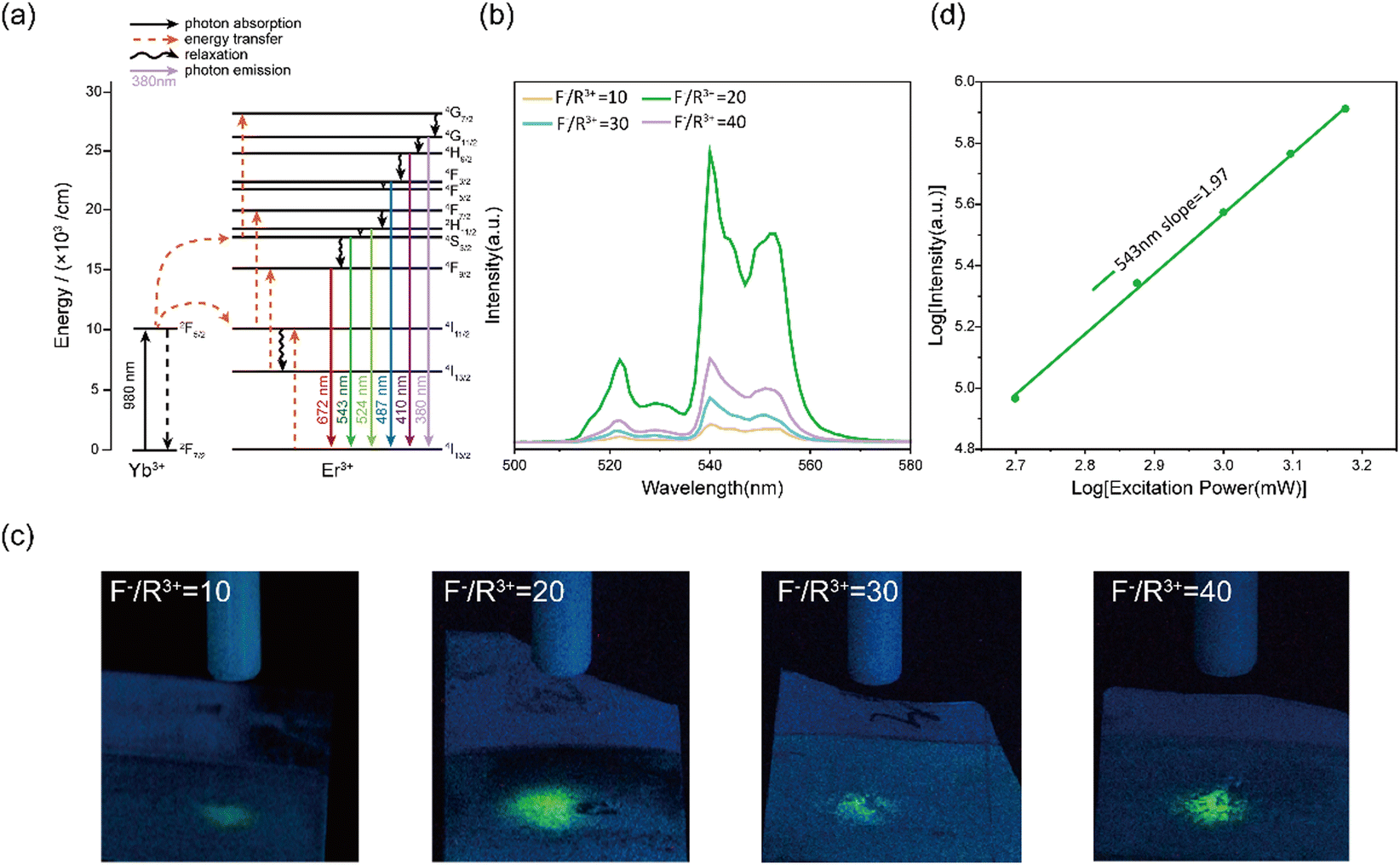 | ||
| Fig. 2 UC photoluminescence properties of NaYF4:Yb3+, Er3+ thin films. (a) Energy transfer mechanism of NaYF4:Yb3+, Er3+ thin films. (b) UC fluorescence spectra of the thin films prepared at different F−/R3+ ratios. (c) Green light emission of the thin films prepared at different F−/R3+ ratios. The excitation wavelength from the optical fiber was 980 nm, the images were collected by using a 600 nm low-pass filter. (d) The relationship between green light emission power and NIR excitation power of the thin films. | ||
Next, we focused on the NaYF4:Yb3+, Er3+ thin films prepared at an F−/R3+ ratio of 20 because of their high conversion efficiency from NIR to green light. We investigated the UC mechanism of the thin films prepared at an F−/R3+ ratio of 20. The emission power was recorded as a function of the excitation power at 980 nm. For an UC process, the relationship between the emission power (I) and excitation power (P) can be described as
| I ∝ Pn |
Design and assembly of flexible neural devices
Flexible neural devices based on NaYF4:Yb3+, Er3+ thin films were fabricated by standard microfabrication and electrodeposition techniques (Fig. S1, ESI†). Polyimide was chosen as the flexible substrate owing to its excellent insulation properties and biocompatibility. Each flexible microelectrode array consisted of a free-standing distal segment for signal recording and a proximal I/O area for electrical interconnection (Fig. S5, ESI†). As shown in Fig. 3a, the free-standing segment of flexible microelectrode array consisted of 8 longitudinal filaments with a total thickness of ca. 4 μm. The recording microelectrodes had a semicircular arch shape and were distributed on the longitudinal filaments across a depth of 1.5 mm. To reduce thermal noise, the recording microelectrodes were electroplated by nano-sized platinum to achieve electrochemical impedance of 71.7 ± 21.8 kΩ at 1 k Hz (Fig. 3b and c, and Fig. S6, ESI†). NaYF4:Yb3+, Er3+ thin films, with a width of 44 μm and length of 2 mm, were electrodeposited on the longitudinal filaments to co-localize with the recording microelectrodes (Fig. 3d). The as-formed NaYF4:Yb3+, Er3+ thin film consisted of nanoparticles with an average diameter of 500 nm (Fig. 3e). The surface roughness of NaYF4:Yb3+, Er3+ thin film was ca. 228 nm as determined by AFM measurements (Fig. 3f). After electrodeposition, the UC thin films were sandwiched between two PI layers for encapsulation.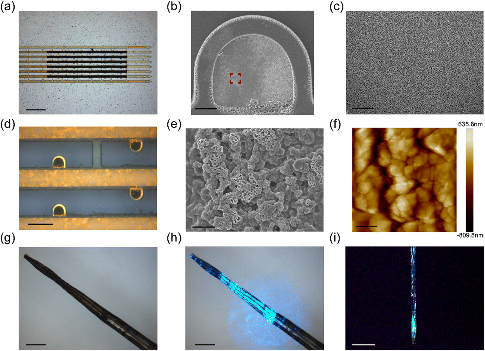 | ||
| Fig. 3 Flexible neural devices. (a) Photograph of an as-fabricated flexible device. Scale bar, 500 μm. (b) SEM image of nano-platinum modified recording microelectrodes. Scale bar, 10 μm. (c) Magnified view of the region highlighted in the red box in b. Scale bar, 2 μm. (d) Zoomed-in view of recording microelectrodes and UC thin film sections. Scale bar, 40 μm. (e) Morphology of electrodeposited NaYF4:Yb3+, Er3+ thin film on the device. Scale bar, 5 μm. (f) AFM image of electrodeposited NaYF4:Yb3+, Er3+ thin film. Scale bar, 1 μm. (g) Photograph of an assembled flexible device encapsulated in the PEG polymer. Scale bar, 500 μm. (h) The assembled flexible neural device with blue light illumination. Scale bar, 500 μm. (i) The assembled flexible neural device under 980 nm NIR light illumination. The photograph was taken under a 600 nm low-pass filter. Scale bar, 500 μm. | ||
One of the major challenges of flexible devices during implantation is their susceptibility to deformation under mechanical stress. To address this challenge, we adopted an elastocapillary self-assembly strategy to encapsulate each flexible neural device, together with an optical fiber, within a dissolvable PEG polymer carrier (Fig. 3g). The assembled device formed a solidified fiber with a diameter of approximately 200 μm. The tip of the optical fiber was positioned about 3 mm above the distal end of the flexible microelectrode array, as confirmed by the blue light illumination image in Fig. 3h. We further characterized the photoluminescence properties of the assembled device under NIR illumination. As shown in Fig. 3i, the UC film in the assembled device exhibited green fluorescence under 980 nm NIR illumination, and the green light was spatially localized around the UC film region.
NIR optogenetics and electrophysiological recordings
Electrodeposited NaYF4:Yb3+, Er3+ thin films in the assembled device can convert NIR light into green light to manipulate the activity of C1V1 opsin. Next, we evaluated the capabilities of our flexible devices for simultaneous optogenetics and electrophysiology. We injected an AAV9-hSyn::C1V1-mCherry virus solution into the M2/VO region of wild-type mice (n = 3). The AAV9-hSyn::C1V1-mCherry virus carries an excitatory C1V1 opsin that is used with the fluorescent mCherry protein. An assembled flexible neural device was then implanted into the same brain region. Owing to the mechanical support of the PEG carrier, the assembled device could be readily implanted into the targeted brain regions. After implantation, the PEG carrier was dissolved by cerebrospinal fluid, and the flexible microelectrodes were released to form a mechanically compatible interface with soft brain tissues. The optical fiber was kept above the brain surface to reduce both acute and chronic tissue damages.Representative electrophysiological recording results are highlighted in Fig. 4a–c. We were able to isolate 56 single units from 36 recording channels with high signal-to-noise ratio (SNR) at two weeks post implantation. These results highlight the capability of the flexible microelectrodes to form intimate interfaces with neuronal cells in the brain. We then investigated the capability of the flexible neural device for NIR-based optogenetic stimulation. Mice were subjected to pulsed NIR light stimulation (980 nm, 20 ms, 10 Hz, 14.33 W mm−2 for pulsed stimulation). As shown in Fig. 4d, the spiking activities of C1V1-expressing neurons could be effectively manipulated by the pulsed NIR light at four weeks post-implantation, highlighting the up-conversion capability of the electrodeposition NaYF4:Yb3+, Er3+ films. In addition, the average waveforms of recorded single-unit spikes were not affected by NIR stimulations, as shown in Fig. 4e, indicating that NIR light could modulate the activities of C1V1-expressing neurons without thermal damages.
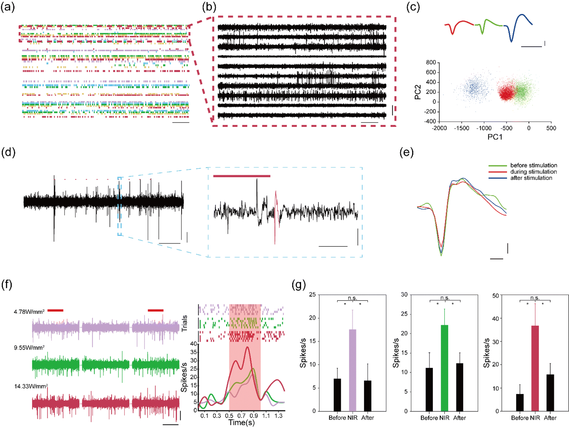 | ||
| Fig. 4 Simultaneous electrophysiological recordings and NIR optogenetics. (a) Raster plots recorded on a 61-channel flexible neural device in the mouse M2/VO region at 2 weeks post-implantation. Scale bar, 500 ms. (b) Action potential traces of representative channels at 2 weeks post-implantation. Scale bars, 500 ms (horizontal) and 100 μV (vertical). (c) Waveforms and PCA clusters of single-units sorted from channel 60. Scale bars, 1 ms (horizontal) and 20 μV (vertical). (d) Firing responses to 10 Hz 20 ms 980 nm pulsed light. Scale bar, 200 ms (horizontal) and 10 μV (vertical), 10 ms (horizontal) and 20 μV (vertical) in magnified views. (e) Average waveforms collected before, during, and after NIR stimulation. Scale bar, 200 μs (horizontal) and 10 μV (vertical). (f) Firing response to continuous 980 nm light stimulation. Scale bars, 500 ms (horizontal) and 20 μV (vertical). (g) Quantitative analysis of firing rates before, during, and after NIR stimulation (*p < 0.01). | ||
We further investigated the manipulation capacity of the flexible device under continuous NIR light stimulation (980 nm, 500 ms, 0.1 Hz, 4.78–14.33 W mm−2). We found that the firing rates of the recorded neurons were enhanced from 8 spikes s−1 to 38 spikes s−1 when the power density of the NIR light was increased from 4.78 to 14.33 W mm−2 (Fig. 4f). These results further confirmed that the UC films could effectively convert NIR light into green light for the activation of the C1V1 opsins. In addition, quantitative analysis of the firing rates showed that the spiking activities of the recorded neurons restored to normal level after continuous NIR stimulation (Fig. 4g). Collectively, these results confirm that the flexible neural devices can allow for combined NIR manipulation with electrophysiological recording in a minimally invasive manner.
Conclusions
In this study, we developed flexible neural devices by integrating polymer-based microelectrode arrays with UC thin films for simultaneous neural recording and NIR optogenetic manipulation. By combining microfabrication and electrodeposition technologies, NaYF4:Yb3+, Er3+ UC films were spatially co-localized with the recording microelectrodes. Under out-of-brain NIR light stimulation, the UC layer in the flexible device could convert NIR light into green light for the activation of C1V1 opsin-expressing neurons. As a result, chronically implanted devices achieved simultaneous NIR optogenetics and electrophysiology in the brain. The low invasiveness and good biocompatibility of the flexible UC devices make them an attractive candidate for chronic neural manipulation and recording.The brain consists of multiple types of neuronal cells that are integrated into complex neural circuits. Our flexible neural device can be easily integrated with different UC materials, thus providing a route towards selective activation of different neuronal populations. For example, NaYF4:Yb3+: Tm3+ films and NaYF4:Yb3+: Nb3+: Er3+ films can be selectively electrodeposited in different regions of a flexible device for the activation of ChR2 opsins and suppression of NpHR opsins under 980 nm and 808 nm NIR light excitation, respectively. Moreover, our devices can be applied for NIR-triggered drug delivery by capping photo-switchable units onto drug-coated UC films. Under NIR light stimulation, the UC films of the flexible device can convert NIR light to visible light and thus lead to controllable release of drugs into the brain for both neural mechanism analysis and treatment of neurological disorders. We foresee that these advancements can enrich the toolbox of both basic and applied neuroscience research.
Conflicts of interest
There are no conflicts to declare.Acknowledgements
We thank the Fabrication Lab at NCNST for the microfabrication facilities and support, and the Animal Resource Center at NCNST for animal housing and care. This work is supported by the National Natural Science Foundation of China (Grant No. 61971150, 32061143013 and 22102040), and the Major project of scientific and technological Innovation of 2030 (Grant No. 2021ZD0202200 and 2021ZD0202201).Notes and references
- G. Shin, A. M. Gomez, R. AI-Hasani, Y. R. Jeong, J. Kim, Z. Xie, A. Banks, S. M. Lee, S. Y. Han, C. J. Yoo, J. L. Lee, S. H. Lee, J. Kurniawan, J. Tureb, Z. Guo, J. Yoon, S. I. Park, S. Y. Bang, Y. Nam, M. C. Walicki, V. K. Samineni, A. D. Mickle, K. Lee, S. Y. Heo, J. G. McCall, T. Pan, L. Wang, X. Feng, T. I. Kim, J. K. Kim, Y. Li, Y. Huang, R. W. Gereau, J. S. Ha, M. R. Bruchas and J. A. Rogers, Neuron, 2017, 93, 509–521 CrossRef CAS PubMed.
- T. I. Kim, J. G. McCall, Y. H. Jung, X. Huang, E. R. Siuda, Y. H. Li, J. Z. Song, Y. M. Song, H. A. Pao, R. H. Kim, C. F. Lu, S. D. Lee, I. S. Song, G. Shin, R. Al-Hasani, S. Kim, M. P. Tan, Y. Huang, F. G. Omenetto, J. A. Rogers and M. R. Bruchas, Science, 2013, 340, 211–216 CrossRef CAS PubMed.
- F. Wu, E. Stark, P. C. Ku, K. D. Wise, G. Buzsáki and E. Yoon, Neuron, 2015, 88, 1136–1148 CrossRef CAS PubMed.
- F. Zhang, L. P. Wang, M. Brauner, J. F. Liewald, K. Kay, N. Watzke, P. G. Wood, E. Bamberg, G. Nagel, A. Gottschalk and K. Deisseroth, Nature, 2007, 446, 633–639 CrossRef CAS PubMed.
- L. Zou, H. Tian, S. Guan, J. Ding, L. Gao, J. Wang and Y. Fang, Nat. Commun., 2021, 12, 5871 CrossRef CAS PubMed.
- S. Golovynskyi, I. Golovynska, L. I. Stepanova, O. I. Datsenko, L. Liu, J. Qu and T. Y. Ohulchanskyy, J. Biophotonics, 2018, 11, e201800141 CrossRef PubMed.
- X. Wu, Y. Zhang, K. Takle, O. Bilsel, Z. Li, H. Lee, Z. Zhang, D. Li, W. Fan, C. Duan, E. M. Chan, C. Lois, Y. Xiang and G. Han, ACS Nano, 2016, 10, 1060–1066 CrossRef CAS PubMed.
- S. Shah, J. J. Liu, N. Pasquale, J. Lai, H. McGowan, Z. P. Pang and K. B. Lee, Nanoscale, 2015, 7, 16571–16577 RSC.
- Y. Ao, K. Zeng, B. Yu, Y. Miao, W. Hung, Z. Yu, Y. Xue, T. T. Y. Tan, T. Xu, M. Zhen, X. Yang, Y. Zhang and S. Gao, ACS Nano, 2019, 13, 3373–3386 CrossRef CAS PubMed.
- N. Yu, L. Huang, Y. Zhou, T. Xue, Z. Chen and G. Han, Adv. Healthcare Mater., 2019, 8, 1801132 CrossRef PubMed.
- S. Chen, A. Z. Weitemier, X. Zeng, L. M. He, X. Y. Wang, Y. Q. Tao, A. J. Y. Huang, Y. Hashimotodani, M. Kano, H. Iwasaki, L. K. Parajuli, S. Okabe, D. B. L. Teh, A. H. All, I. Tsutsui-Kimura, K. F. Tanaka, X. G. Liu and T. J. McHugh, Science, 2018, 359, 679–683 CrossRef CAS PubMed.
- Y. Ma, J. Bao, Y. Zhang, Z. Li, X. Zhou, C. Wan, L. Huang, Y. Zhao, G. Han and T. Xue, Cell, 2019, 177, 243–255 CrossRef CAS PubMed.
- T. Miyazaki, S. Chowdhury, T. Yamashita, T. Matsubara, H. Yawo, H. Yuasa and A. Yamanaka, Cell Rep., 2019, 26, 1033–1043 CrossRef CAS PubMed.
- Y. Pu, L. F. Lin, D. Wang, J. X. Wang, J. Qian and J. F. Chen, J. Colloid Interface Sci., 2018, 511, 243–250 CrossRef CAS PubMed.
- S. Jeon, Y. Lee, D. Ryu, Y. K. Cho, Y. Lee, S. B. Jun and C. H. Ji, Micromachines, 2021, 12, 725 CrossRef PubMed.
- J. J. Jun, N. A. Steinmetz, J. H. Siegle, D. J. Denman, M. Bauza, B. Barbarits, A. K. Lee, C. A. Anastassiou, A. Andrei, Ç. Aydın, M. Barbic, T. J. Blanche, V. Bonin, J. Couto, B. Dutta, S. L. Gratiy, D. A. Gutnisky, M. Häusser, B. Karsh, P. Ledochowitsch, C. M. Lopez, C. Mitelut, S. Musa, M. Okun, M. Pachitariu, J. Putzeys, P. D. Rich, C. Rossant, W. L. Sun, K. Svoboda, M. Carandini, K. D. Harris, C. Koch, J. O’Keefe and T. D. Harris, Nature, 2017, 551, 232 CrossRef CAS PubMed.
- B. Z. Li, K. Lee, S. C. Masmanidis and M. Li, J. Neural Eng., 2018, 15, 046008 CrossRef PubMed.
- P. H. Fan, Y. L. Song, S. W. Xu, Y. C. Dai, Y. D. Wang, B. T. Lu, J. Y. Xie, H. Wang and X. X. Cai, Sensors, 2020, 20, 4526 CrossRef CAS PubMed.
- P. J. Rousche and R. A. Normann, J. Neurosci. Methods, 1998, 82, 1–15 CrossRef CAS PubMed.
- V. S. Polikov, P. A. Tresco and W. M. Reichert, J. Neurosci. Methods, 2005, 148, 1–18 CrossRef PubMed.
- P. Moshayedi, G. Ng, J. C. Kwok, G. S. Yeo, C. E. Bryant, J. W. Fawcett, K. Franze and J. Guck, Biomaterials, 2014, 35, 3919–3925 CrossRef CAS PubMed.
- J. W. Salatino, K. A. Ludwig, T. D. Y. Kozai and E. K. Purcell, Nat. Biomed. Eng., 2017, 1, 862–877 CrossRef CAS PubMed.
- J. L. Zhuang, J. Wang, X. F. Yang, I. D. Williams, W. Zhang, Q. Y. Zhang, Z. M. Feng, Z. M. Yang, C. L. Liang, M. M. Wu and Q. Su, Chem. Mater., 2009, 21, 160–168 CrossRef CAS.
- H. X. Mai, Y. W. Zhang, R. Si, Z. G. Yan, L. D. Sun, L. P. You and C. H. Yan, J. Am. Chem. Soc., 2006, 128, 6426–6436 CrossRef CAS PubMed.
- S. Suzuki, K. Teshima, T. Wakabayashi, H. Nishikiori, T. Ishizaki and S. Oishi, J. Mater. Chem., 2011, 21, 13847 RSC.
- W. Shao, R. Hua, W. Zhang, Y. Tian, J. Zhao, L. Na, J. Yu and Z. Sun, Powder Technol., 2013, 237, 326–332 CrossRef CAS.
- G. Chen, W. Shao, R. R. Valiev, T. Y. Ohulchanskyy, G. S. He, H. Ågren and P. N. Prasad, Adv. Opt. Mater., 2016, 4, 1760–1766 CrossRef CAS.
- A. Karami, F. Farivar, T. J. de Prinse, H. Rabiee, S. Kidd, C. J. Sumby and J. Bi, ACS Appl. Bio Mater., 2021, 4, 6125–6136 CrossRef CAS PubMed.
- Y. J. Ding, H. Zhu, X. X. Zhang, J. J. Zhu and C. Burda, Chem. Commun., 2013, 49, 7797–7799 RSC.
- D. M. Yang, C. X. Li and J. Lin, Nanomedicine, 2015, 10, 2573–2591 CrossRef CAS PubMed.
- S. Han, A. Samanta, X. J. Xie, L. Huang, J. J. Peng, S. J. Park, D. B. L. Teh, Y. Choi, Y. T. Chang, A. H. All, Y. M. Yang, B. G. Xing and X. G. Liu, Adv. Mater., 2017, 29, 1700244 CrossRef PubMed.
- X. Liu, H. Chen, Y. Wang, Y. Si, H. Zhang, X. Li, Z. Zhang, B. Yan, S. Jiang, F. Wang, S. Weng, W. Xu, D. Zhao, J. Zhang and F. Zhang, Nat. Commun., 2021, 12, 5662 CrossRef CAS PubMed.
- Y. Wang, K. Xie, H. B. Yue, X. Chen, X. Luo, Q. H. Liao, M. Liu, F. Wang and P. Shi, Nanoscale, 2020, 12, 2406–2414 RSC.
- H. Jia, C. Xu, J. Wang, P. Chen, X. Liu and J. Qiu, CrystEngComm, 2014, 16, 4023–4028 RSC.
- M. Alkahtani, H. Qasem, S. M. Alenzi, N. Alsofyani, A. Alfahd, A. Aljuwayr and P. R. Hemmer, Nanomaterials, 2022, 12, 2115 CrossRef CAS PubMed.
- X. Qu, G. Pan, H. K. Yang, Y. Chen, J. W. Chung, B. K. Moon, B. C. Choi and J. H. Jeong, Opt. Mater., 2012, 34, 1007–1012 CrossRef CAS.
- C. Liu, H. Wang, X. Li and D. Chen, J. Mater. Chem., 2009, 19, 3546–3553 RSC.
- I. Z. Dinic, M. E. Rabanal, K. Yamamoto, Z. Tan, S. Ohara, L. T. Mancic and O. B. Milosevic, Adv. Powder Technol., 2016, 27, 845–853 CrossRef CAS.
- F. Wang and X. Liu, Chem. Soc. Rev., 2009, 38, 976–989 RSC.
Footnotes |
| † Electronic supplementary information (ESI) available. See DOI: https://doi.org/10.1039/d2tb02665a |
| ‡ These authors contributed equally to this work. |
| This journal is © The Royal Society of Chemistry 2023 |