
Oxysalt based synergistic dual interfacial engineering for high performance p–i–n structured perovskite solar cells†
Pramila
Patil
,
Sung-Nam
Kwon
,
Sushil S.
Sangale
,
Dilpreet Singh
Mann
and
Seok-In
Na
 *
*
Department of Flexible and Printable Electronics, LANL-CBNU Engineering Institute-Korea, Jeonbuk National University, 567, Baekje-daero, Deokjin-gu, Jeonju-si, Jeollabuk-do 54896, Republic of Korea. E-mail: nsi12@jbnu.ac.kr
First published on 28th November 2023
Abstract
Inverted perovskite solar cells (IPeSCs) have attracted extensive attention due to low-temperature processability and prospects for scale-up production. However, the power conversion efficiency (PCE) of IPeSCs lags compared to normal architecture, which is mainly due to inadequate interfaces of charge transport layers, viz electron and hole transport layers (ETL and HTL) and perovskite that suffers from carrier recombination paving the way for bulk recombination impeding the PCE and long-term stability of small devices. It is crucial to introduce an effective technique to reduce the interfacial non-radiative recombination losses at both interfaces of the perovskite layer. In this work, we demonstrated a multifunctional strategy to passivate the interface defects via the interactions and synergistic effect of anions and cations produced from sodium nitrate (NaNO3), a π-conjugated oxysalt, at HTL/perovskite and ETL/perovskite interfaces. The synergistic effect of cation and anion bonding and interaction was confirmed by various experimental studies that decreased defect densities and improved the transfer of charges. The synergistic effect with double-side passivated devices showed a champion PCE of 21.53% as compared to pristine (19.08%), bottom (20.16%), and top (20.83%) passivated devices. The π-conjugated oxysalt also improved the IPeSC stability by building a moisture-resistant interface. This work signifies the effect of chemical bonding engineering via cations and anions at dual-perovskite interfaces for synergistically enhanced PCE and long-term stability of IPeSCs.
1. Introduction
Perovskite solar cells (PeSCs), which are the youngest generation of photovoltaic devices, have experienced an unparalleled surge in recent years due to the cost-effective and easy processing techniques, their tunable band gap, and the fact that they are made using readily available organic/inorganic materials that are compatible with industrial processing; as a result, they have arisen as the most encouraging industrial photovoltaic technology.1–3The inverted structure of PeSCs, i.e., positive–intrinsic–negative (p–i–n), has attracted substantial attention due to its potential utility in flexible and tandem devices due to its low-temperature processability.4 Despite the immense attention that has been paid to the inverted solar cell configuration (IPeSC), the power conversion efficiency (PCE) values of IPeSCs still lag compared to those of the standard architecture, i.e., the n–i–p structure.5 The primary reasons for the decreased performance of IPeSCs are associated with diminished charge extraction and increased non-radiative recombination losses. These issues arise from factors such as mismatched energy band alignment, the presence of interfacial defects, and the presence of trap sites, all of which collectively limit the device's fill factor and photovoltage.6 To tackle these challenges, extensive research attempts are currently in progress to devise strategies for mitigating defects, including point defects, surface defects, and bulk trap defects.7,8 The charge transport layers (CTLs) and the perovskite interface are the most crucial interfaces, as the growth of perovskite films and charge transportation depend on these interfaces. In p–i–n-structured PeSCs, NiO is most commonly used as a hole transport layer (HTL) owing to its wide band gap and deep valence band maximum (VBM) values, while [6,6]-phenyl C61-butyric acid methyl ester (PCBM) has been identified as an electron transport layer (ETL) due to its outstanding charge transport abilities as well as low-temperature solution processability.9 However, the chemical species (such as water molecules and hydroxyl groups) and surface charge defects at the NiO surface can result in charge recombination, thereby reducing the open circuit voltage (Voc) and fill factor (FF), while the low solubility and viscosity of PCBM can lead to a low-quality non-uniform film on perovskite.9,10 These issues result in charge accumulation, recombination, and inefficient charge extraction, thus leaving perovskite vulnerable to degradation, which in turn limits device performance and serves as an obstacle to obtaining high PCE.
To date, several approaches have been used to modulate the interfaces of CTLs with the perovskite, such as solvent engineering, perovskite composition engineering, additive engineering, anti-solvent additive engineering, interface engineering, etc.11–15 Among the available options, interface engineering is an efficient strategy to enhance perovskite film quality via modulating the growth and nucleation process. However, it could be highly desirable to identify a molecule that is also suitable for passivating the defects within the perovskite layer. The use of ionic compounds (cations and anions) has emerged as a novel strategy to passivate the defects and improve the interface quality. For instance, Bang et al. reported sodium bis(trifluoromethanesulfonyl)imide (Na-TFSI), a defect-tolerant dopant that improved both the performance and stability of PeSCs.16 On a similar note, potassium nitrilotriacetate (NTAK) was used in SnO2/perovskite interfaces, where the amino and carboxyl groups interacted with SnO2 and undercoordinated Pb2+ in the perovskite layer and simultaneously improved crystallization and passivated defects, accordingly, improving device performance and stability.17 Zhang et al. evaporated potassium chloride salt (KCl) at both the HTL and ETL interfaces and achieved a champion PCE of 19.2%, eventually resulting in reduced recombination at the defect sites.18 Low-cost alkali salts have demonstrated immense possibility due to the readily available cations and anions passivating both holes and electron trapping defects in the perovskite layer.19,20 For instance, Park et al. evaluated alkali metal iodide series and concluded that K+ ions leads to hysteresis-free PeSCs.21 Moreover, Zang et al. used potassium sulphate (K2SO4), in regular PeSCs as a multifunctional layer to improve the SnO2/perovskite interface. The SO42− coordinated with Pb2+ at the bottom interface, while the K+ ion diffused into the perovskite layer, subsequently passivating the interfacial defects and modulating the energy level alignment. Hence, a synergistic effect of K+ and SO42− was achieved in realizing high-performance PeSCs.22 Similarly, Li et al. utilized a π-conjugated oxysalt, i.e., potassium carbonate (K2CO3), for the interfacial molecule binder and defect free layer at the SnO2/perovskite interface in n–i–p PeSCs. The π-conjugated oxysalt interlayer offered a robust interface that enhanced the device stability and achieved impressive PCE.23
Although there have been various reports demonstrating modification at HTL/perovskite or ETL/perovskite interfaces using a suitable strategy, there is yet to be a strategy demonstrating interfacial engineering that utilizes both cations and anions from the same salt used at both HTL and ETL interfaces with perovskite in IPeSCs to improve the device performance. It is therefore urgently necessary to investigate the most suitable and multifunctional ionic compound to build a strong interface having reduced defect density, diminished charge recombination, and a synergistic effect for high performance IPeSCs.
Herein, we believe that we have demonstrated for the first time a cost-effective, simple yet effective interfacial modifier sodium nitrate (NaNO3, ionic compound), a π-conjugated oxysalt, so that the collaborative effect of cation and anion interaction from both ends could contribute to the formation of robust interface layers. The introduction of NaNO3 at both charge transfer interfaces promoted the growth of superior perovskite films at the HTL interface along with improved charge transport properties at the ETL interface. The detailed experimental studies of both the bottom and top-side passivated devices along with double-side passivated devices revealed improved charge transfer properties with reduced defect density and recombination at the interfaces. The optimized double-side passivated device showed a champion PCE of 21.53% with enhanced Voc, FF and short-circuit current density (Jsc) compared to the pristine, bottom, and top-side passivated devices. Moreover, the stability of the devices exhibited remarkable long-term light and nitrogen stability for unencapsulated devices.
2. Results and discussion
In designing the scientific approach for the two-fold optimization of the triple cation-based perovskite layer's interfaces, we use sodium nitrate ionic solution as the dual modifier for both HTL and ETL interfaces with the perovskite. Fig. 1a shows the schematics of the device architecture with the sodium nitrate surface passivator on dual sides of the photoactive layer. The HTL side (bottom-side passivated devices) and ETL side (top-side passivated devices) are designated as BSP and TSP, respectively. The dual-side passivated devices are designated as DSP. Materials and experimental procedures are described in depth in the ESI documentation.†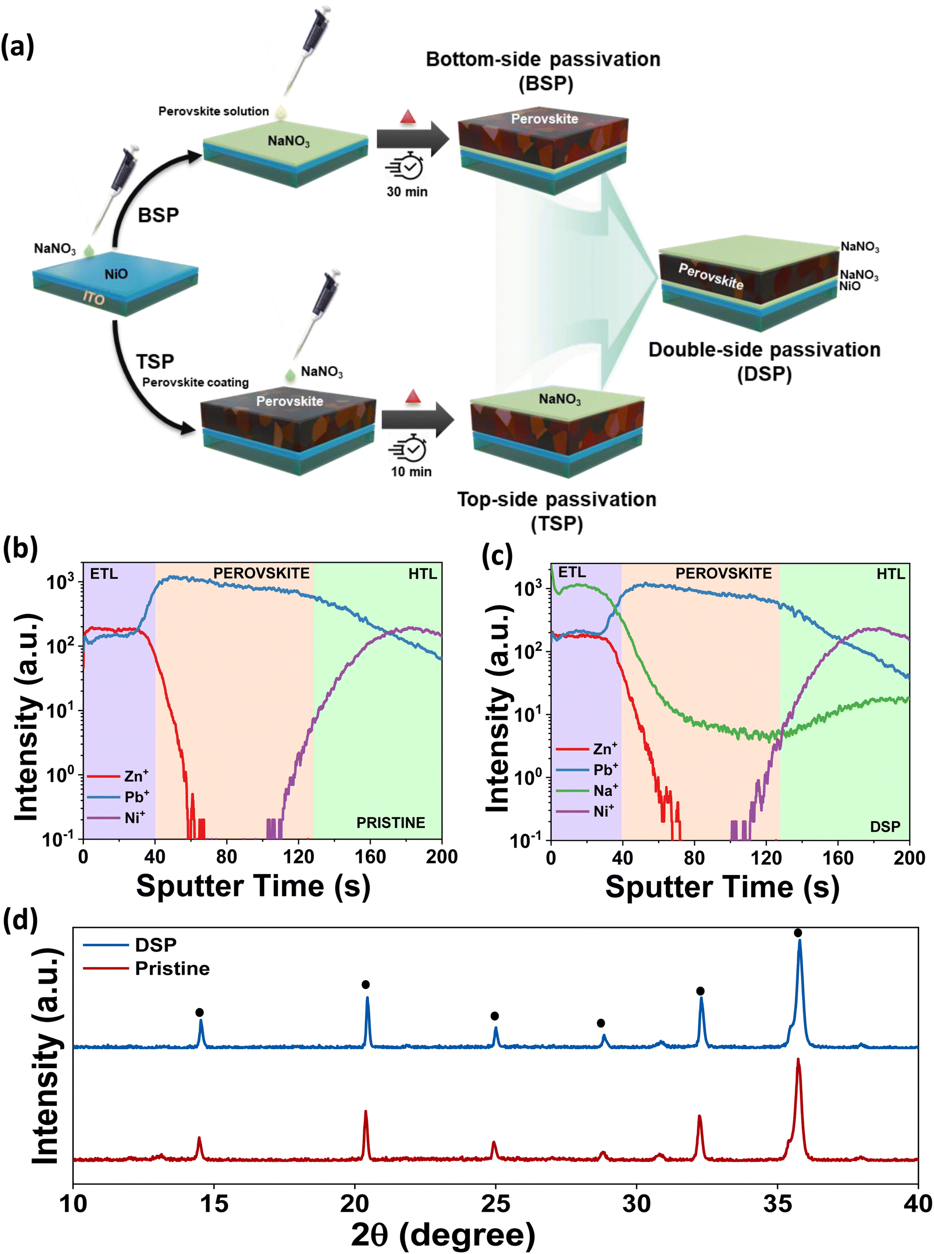 | ||
| Fig. 1 (a) Schematic illustration showing the fabrication of bottom passivated (BSP), top passivated (TSP) and double side passivated (DSP) layers. TOF-SIMS depth profiles (from surface to bottom) of perovskite films: (b) pristine and (c) DSP films. (d) XRD patterns for perovskite films for pristine and DSP perovskite layers. | ||
To ascertain the distribution of NaNO3 in the entire device, we performed time of flight secondary ion mass spectrometry (ToF-SIMS). The depth profiling images of the main elements were obtained and are shown in Fig. 1b and c. The depth profile images for DSP reveal that the sodium ions are mainly located at the interfaces of the HTL and ETL. Fig. 1c clearly shows the distribution of diffusion of Na ions at the interfaces and in the bulk for the DSP samples. The distribution along the interface reveals that the interaction mostly occurs at the interfaces leading to interfacial bonding, while the diffusion of Na ions in the bulk could also help passivate the bulk defects.18,24
Furthermore, XRD analysis was conducted to examine the effect of alkali salt solution treatment on the structural characteristics of perovskite films. The perovskite films in pristine and DSP are shown in Fig. 1d. Both samples exhibited a nearly identical orthorhombic perovskite crystal structure, without apparent shift of the perovskite phase, implying that neither Na+ nor NO3− has been incorporated in the perovskite crystal lattice.11,25 The small PbI2 signals in pristine samples deposited on the NiO surface disappeared in the NiO/NaNO3-based perovskite films, indicating that introducing NaNO3 can effectively restrict the interfacial reactions.26 There was an observable increase in the intensity of the perovskite films deposited on the NiO/NaNO3 surface, implying that the crystallinity of the perovskite films was improved. This further indicates that the crystal orientation was controlled in an efficient way to decrease the distortions in lattice and micro-strains in crystals and ultimately reduce the formation of traps and defects.27,28 To analyze the effect of NaNO3, XRD analysis of the sample without heating of the perovskite films was also carried out. We observed that even without heating, the XRD peak intensity in the case of DSP was significantly improved in comparison to pristine, as shown in Fig. S1.† The FWHM also decreased significantly, indicating an increase in the crystallite size. The FWHM for the perovskite layer with and without heat is shown in Table S1.† As previous studies have speculated,29,30 the dissolved salt can retard the heterogeneous nucleation process occurring at the HTL and perovskite interface, thus leading to an enlarged perovskite crystallite size. Therefore, the crystallite size was found to increase even without heating the perovskite layer.29,31 Ultimately, the dual passivation strategy enhanced crystallinity and increased grain size, which is anticipated to lower defect density and inhibit recombination.
2.1 HTL interface engineering
The HTL interface interactions were studied in detail to elucidate the effect of NaNO3 as an HTL interfacial layer. In this process, X-ray photoelectron spectroscopy (XPS) was carried out to investigate various chemical properties and more deeply understand the interaction of NaNO3 with the NiO lattice. The XPS spectra are illustrated in Fig. 2a and b. In the figure it can be seen that the XPS spectra shifted to lower binding energy after treatment of NaNO3 solution on the NiO surface, indicating the possibility of a chemical interaction between NiO and NaNO3, as can be noticed in Fig. S2a and b.† The Ni 2p3/2 characteristic peaks at 854.06 and 855.78 eV shift to the lower binding energy values of 853.81 and 855.38 eV, respectively, after NaNO3 solution treatment. As reported previously, alkali metal ions tend to occupy the interstitial and oxygen vacancy (Ov) sites in metal oxide semiconductors. Huang et al. reported on the formation of interfacial dipoles at ITO/alkali interfaces.33 Similarly, Tai et al. reported on the formation of a Zn–O–Na/K bond by the replacement of H from the –OH group. These permanent dipole moments could alter the distribution of the electrical charges on the surface.32–34 Analogously, we speculate from previous reports that Na+ ions could interact with the hydroxyl groups at the NiO surface and reduce Ov. With detailed analysis of the Ni 2p3/2 and O 1s spectra, we further confirmed the possible interaction. The fitted Ni 2p3/2 XPS spectra showed three peaks corresponding to NiO at 853.8, Ni2O3 at 855.4 eV, and NiOOH at 856.5 eV. As observed in Fig. 2a, after NaNO3 treatment, the relative composition of NiO and NiOOH decreased, whereas the amount of Ni2O3 increased. Similarly, in the O 1s spectrum, the XPS peak at 531 eV may be attributable to the metal deficiency of Ni3+ or excess oxygen of NiOOH. More explicitly, the ratio of Ni2O3/NiO in the case of the NaNO3-treated layer was calculated to be 0.59, compared to the value of 0.49 calculated for the NiO layer. Meanwhile, the ratio of NiOOH was reduced from 0.43 to 0.39 for the NiO and NiO/NaNO3 layers, respectively, suggesting that the sodium ion could help to minimize the high valence nickel ions at the NiO surface layer. These observations are consistent with the O 1s spectra, and they further confirm that the Na ions could react with adsorbed hydroxyl groups at the NiO surface4 (Table S2†). These results show that NaNO3 treatment could lead to a reduction in defect sites and hydroxyl groups on top of the HTL surface, ultimately leading to improved charge transfer properties.35 The main reason for the reduction in hydroxyl groups could be the linking of Na with the –OOH group of NiOOH, thus leading to the formation of a Ni–O–Na bond and simultaneously reducing the defect sites and hydroxy groups.32 Furthermore, the Na 1s core-level spectra indicated the presence of a Na peak in the binding energy range of 1072–1073 eV, thereby confirming the presence of Na+ in the modified samples.36 Moreover, nitrate peaks were confirmed on the surface of NiO (Fig. S2c and d†).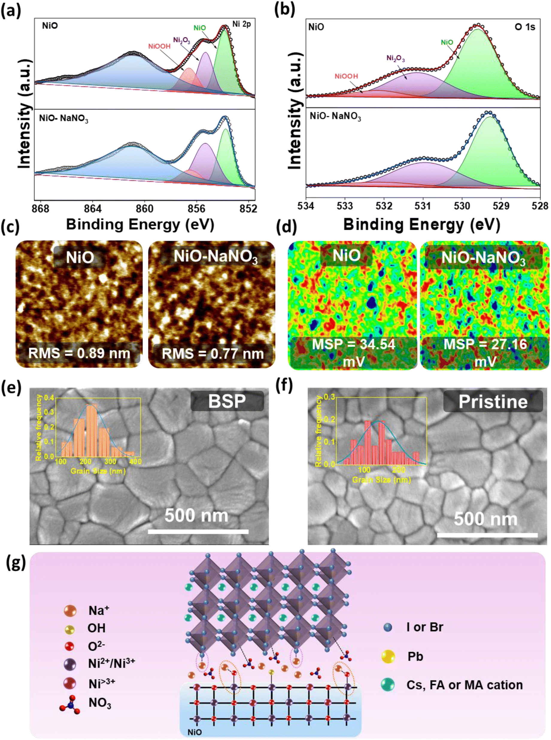 | ||
| Fig. 2 X-ray photoelectron spectroscopy (XPS) spectra of (a) Ni 2p3/2 and (b) O 1s of NiO and NiO-treated with NaNO3. (c) Atomic force microscopy (AFM) and (d) scanning Kelvin probe microscopy (SKPM) images of NiO and NiO treated with NaNO3, (e) FESEM images of the perovskite layer for BSP (inset shows average grain size distribution) and (f) pristine (inset shows average grain size distribution). (g) Probable mechanism for interaction of NaNO3 at the NiO/perovskite interface. | ||
Furthermore, FTIR studies were conducted to understand the mechanism in detail. Fig. S3† shows the FTIR spectra for the NiO, NaNO3, and NiO/NaNO3 films. The NiO film showed a characteristic peak at ∼500 cm−1. The NaNO3 film showed the characteristic peak for antisymmetric stretching vibration at ∼1383 and ∼836 cm−1.37 The deposition of NaNO3 on the NiO surface showed the characteristic peaks of both NiO and NaNO3, indicating that NaNO3 was well anchored on the NiO surface.38 To confirm this, we measured the water contact angles for the NiO and NaNO3 films. The water contact angle was observed to have significantly improved, increasing from 26.44° to 53.17° for control and modified films, respectively (Fig. S4†). This increase in the contact angle also confirms the reduction of surface hydroxyl groups on the NiO film.10 This further supports the XPS and FTIR results indicating that NaNO3 can efficiently reduce the surface hydroxyl groups on the top surface of NiO and ultimately lead to the formation of a better perovskite film.38
Next, Atomic Force Microscopy (AFM) and Scanning Kelvin Probe Microscopy (SKPM) studies were conducted to empathize the impact of NaNO3 treatment further clearly on the surface properties. Some previous reports suggest that bottom passivation could amend the growth of perovskite and influence defect distribution on the perovskite surface and bulk.18Fig. 2c shows topography images of ITO/NiO and ITO/NiO/NaNO3. The surface roughness was reduced from 0.89 nm to 0.77 nm for the NiO/NaNO3-modified samples. Moreover, the surface potential measured from SKPM analysis (Fig. 2d) for ITO/NiO/NaNO3 showed a low value of 27.16 mV, in comparison to the value of 34.54 mV for ITO/NiO. The lower surface potential value suggests that the utilization of NaNO3 can help to improve the work function of NiO. These results support that the holes from the photoactive layer can be more effectively extracted and transported towards the anode.36,39,40
The uniformity of the substrate (NiO) typically represents the most important parameter influencing the film quality and morphology of spin-coated perovskite films. The energy-dispersive X-ray spectroscopy (EDS) mapping images demonstrated the distribution of NaNO3 on the NiO surface. The elements were identified to be evenly distributed on the HTL surface, as represented in Fig. S5.† The surface top-view FESEM analysis of BSP and pristine films was conducted to demonstrate the influence of NaNO3 treatment on the surface morphological qualities of the spin-coated perovskite film, as shown in Fig. 2e and f, respectively. Contrasted to perovskite spin-coated on pristine NiO, a smooth and uniform morphology with a greatly increased grain size, from ∼150 nm to over 350 nm, was obtained for NaNO3-treated NiO, as shown in the inset of Fig. 2e and f. This improvement in the grain size correlated well with the contact angle measurements, which revealed the hydrophobic nature of the modified layer, as depicted in Fig. S4.† The contact angle (CA) value for NiO was measured to be 26.44, which significantly improved to 53.14 for NiO/NaNO3. This implies a reduction in nucleation sites for perovskite and promotes crystal growth. This phenomenon is attributed to the homogeneous nucleation and growth of perovskite, ultimately leading to the formation of larger grains.30,41 This suggests that NaNO3 treatment could not only passivate the NiO surface but also increase grain size, reduce trap states at the NiO/perovskite interface, and eliminate grain boundary defects, thus improving the charge carrier extraction leading to devices with improved cell parameters.5,42
Depicting upon the preceding analysis, we propose that, considering the robust ionic bond of NaI/Br, it is reasonable to suggest that Na+ ions from NaNO3 could readily combine to form NaI/Br at the interface of NiO and perovskite.43,44 The NaX (X = I/Br) formed in this way could readily link with PbX2 and act as a nucleus for perovskite growth.43 The above results and observation are consistent with the XRD result of samples without annealing the perovskite layer, thus implying that the Na ions could facilitate perovskite crystal growth even without thermal annealing. FESEM analysis also supports this evidence, where the perovskite grain size was distinctly improved with a smooth morphology. At the same time, the Na ions could replace the hydroxyl groups in NiO with Na, thus forming a Ni–O–Na bond and aiding in the reduction of the hydroxyl groups on the NiO surface (Fig. 2g).
2.2 ETL interface engineering
After gaining insights into the HTL/perovskite interface, we studied the ETL/perovskite interface in terms of the possibility of a reaction at the surface. To this end, XPS measurements were conducted on top of perovskite films after NaNO3 treatment, i.e., for TSP films, to validate the chemical interactions between the photoactive perovskite material and the NaNO3 small molecules. As exhibited in Fig. 3a and b, the characteristic peaks of Pb 4f7/2 and 4f5/2 and N 1s shift clearly toward lower binding energies than the pristine perovskite film, thus indicating the possibility of interactions between perovskite and passivation molecules, implying that the defects are electrostatically passivated.6,45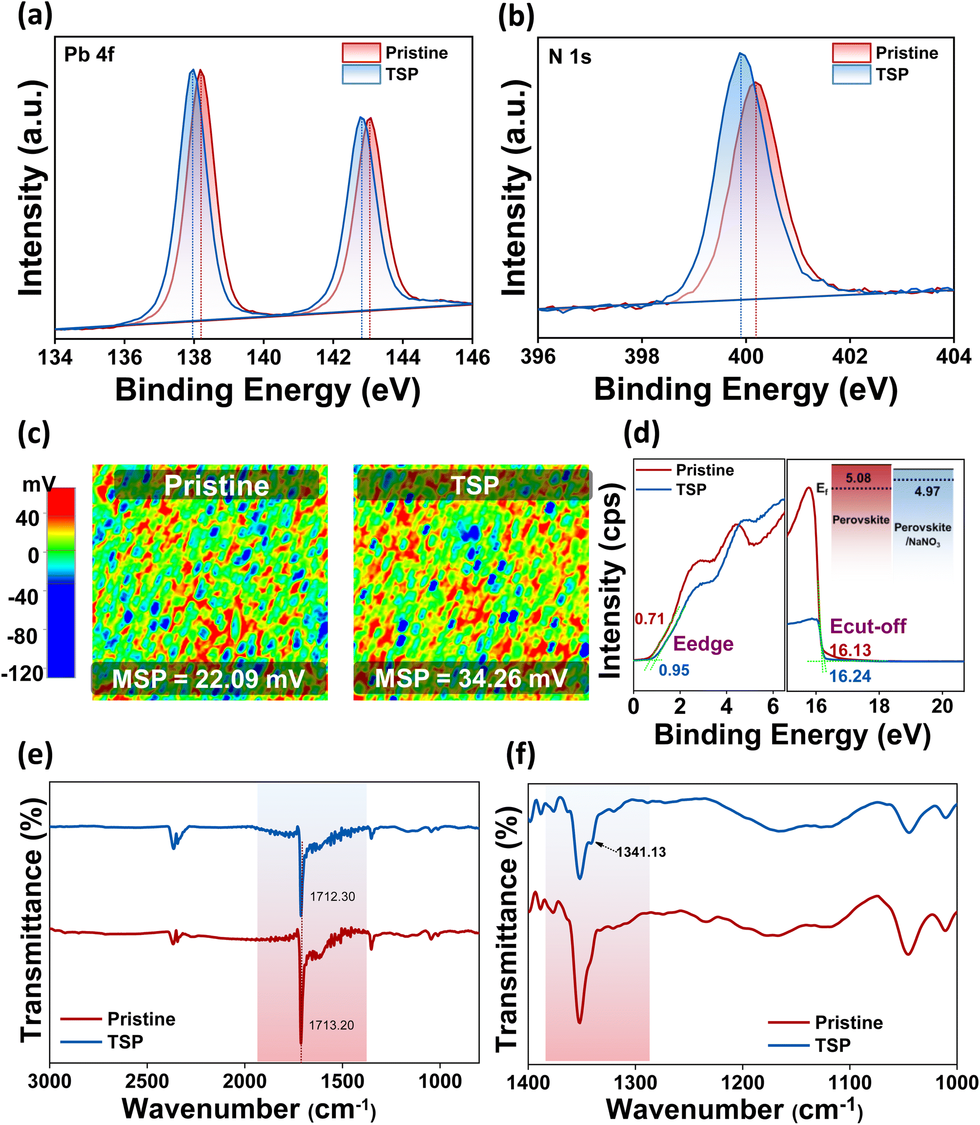 | ||
| Fig. 3 X-ray photoelectron spectroscopy (XPS) spectra of (a) Pb 4f and (b) N 1s. (c) Scanning Kelvin probe microscopy (SKPM) images of pristine and TSP perovskite films. (MSP = mean surface potential). (d) UPS spectra of the perovskite and TSP films (inset shows energy level alignment). (e) FTIR spectra of pristine and TSP films. (f) FTIR spectra of pristine and TSP in the expanded fingerprint region for 1400–1000 cm−1. | ||
Most importantly, the atomic percentage of O 1s improved from 2.64 to 4.11%, as shown in Table S3.† Furthermore, when the relative ratio of iodine and oxygen was calculated, it was observed that the oxygen/iodine ratio increased from 0.0715 (pristine) to 0.119 (TSP). The ratio of oxygen/nitrogen was also found to increase from 0.14 to 0.25 for pristine and TSP samples, respectively. This clearly implies that the relative oxygen percentage is higher even after accounting for the inevitable bonding of oxygen in the environment, and it is evident that sodium nitrate exists on the perovskite's surface.
SKPM and UPS analyses were carried out to study the effect of NaNO3 solution treatment on the electronic states of perovskite. Fig. 3c reveals the surface potential photo-images of pristine and TSP-based perovskite films. As observed from the images, the mean surface potential of the pristine perovskite film was 22 mV, which increased by almost 12 mV and reached 34 mV after NaNO3 treatment. These results indicate that there is an up-shift in the quasi-Fermi level, which is consistent with previous reports.14,46 This trend was in line with the work-function change obtained by UPS analysis (Fig. 3d). The Fermi level of TSP was calculated to be −4.97 eV, whereas that of pristine devices was calculated to be −5.08 eV (inset of Fig. 3d). This up-shift by 0.11 mV implies an increase in the built-in potential that consequently leads to an enhancement in the open-circuit voltage (Voc) of devices.14,47
Similarly, the FTIR analysis of perovskite and perovskite/NaNO3 films was conducted to understand the interactions occurring at the interfaces, as shown in Fig. 3e. The FTIR spectra were consistent with the spectra for triple cation-based perovskite films.48,49 The characteristic –C![[double bond, length as m-dash]](https://www.rsc.org/images/entities/char_e001.gif) N symmetric stretch around ∼1700 cm−1 of perovskite shifted to a lower wavenumber along with reduced intensity, thus indicating the possibility of bonding between the lone pair of electrons available on nitrate ions with perovskite via coordination bonding.46 Furthermore, a small peak appeared around 1341.13 cm−1 with a lower wavenumber shift from its original value (∼1383 cm−1) in the sodium nitrate-treated samples, thus indicating interaction of nitrate ions on the perovskite surface (Fig. 3f). These results correlated well with XPS analysis, further confirming the interaction of nitrate ions on the perovskite surface.
N symmetric stretch around ∼1700 cm−1 of perovskite shifted to a lower wavenumber along with reduced intensity, thus indicating the possibility of bonding between the lone pair of electrons available on nitrate ions with perovskite via coordination bonding.46 Furthermore, a small peak appeared around 1341.13 cm−1 with a lower wavenumber shift from its original value (∼1383 cm−1) in the sodium nitrate-treated samples, thus indicating interaction of nitrate ions on the perovskite surface (Fig. 3f). These results correlated well with XPS analysis, further confirming the interaction of nitrate ions on the perovskite surface.
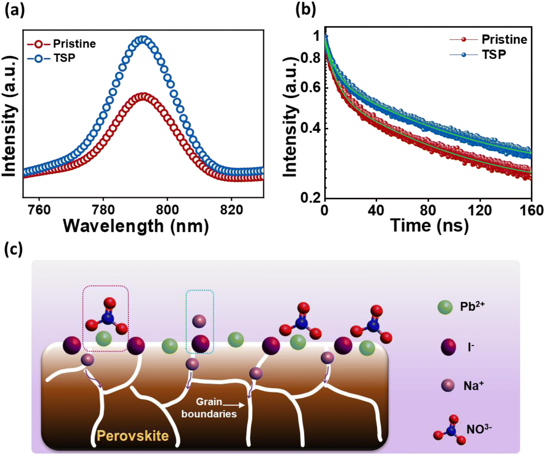
Steady-state photoluminescence (PL) spectroscopy was performed for glass/NiO/perovskite (pristine) and glass/NiO/perovskite/NaNO3 (TSP) films to assess the impact of the passivation strategy on the ultra-fast charge transfer behaviors and the trap states. As exhibited in Fig. 4a, the TSP samples showed a significant increase in PL intensity compared to that of the pristine sample, indicating that the top-side passivated layer reduced the non-radiative recombination of the photogenerated carriers. Furthermore, to ascertain this observation, time-resolved PL (TRPL) and decay transient analyses for pristine and TSP samples were conducted as shown in Fig. 4b. Biexponential functions that correspond to two decay functions were used to fit the TRPL curves.43 The TRPL curves were plotted and fitted with a biexponential decay fitting function, thus resulting in two constituents' system (τ1 (short-lived) and τ2 (long-lived)). The τ1 indicates the monomolecular recombination time span, whereas the τ2 shows the time span for the recombination of charges. The TRPL analysis fitting parameters are summarized in Table S4†. The average lifetime (τPL) of the pristine film was around 40.37 ns, whereas the TSP showed a lifetime of 52.12 ns. TSP perovskite showed a longer carrier lifetime (52.12 ns) than the pristine perovskite sample (40.37 ns), implying that the trap states have been efficiently eliminated for effective charge extraction towards the ETL.50
 | ||
| Fig. 4 (a) PL spectra for pristine and TSP films. (b) TRPL spectra for pristine and TSP films. (c) Probable mechanism for interaction of NaNO3 at the perovskite/ETL interface. | ||
From the above analysis, we propose that there is a possibility that the nitrate group could interact with unreacted Pb2+, which leads to the formation of Pb(NO3)2 as shown in eqn (1).
| Pb2+ + NO3− → Pb(NO3)2 | (1) |
The lead nitrate formed at the surface might serve as a water scavenger and is expected to improve the moisture stability of perovskite.51 Meanwhile, Na+ ions could possibly interact with I− or Br−, thus resulting in the formation of NaI or NaBr.43 Furthermore, Na+ ions could diffuse into the inside perovskite layer, thus passivating the defects within the perovskite layer, as depicted in Fig. 4c.
2.3 Dual interface engineering
The photovoltaic parameters of all passivation strategies were measured at optimal concentrations for passivating the bottom surface (BSP), the top surface (TSP), and both surfaces (DSP). Fig. 5a shows the average performances of pristine, BSP, TSP, and DSP devices. The DSP devices exhibited the best performance justifying the passivation effect on both sides. All other parameters, including Voc, Jsc, and FF, were also improved for the DSP devices compared to the BSP, TSP, and pristine devices (Fig. S6 and Table S5†). Furthermore, to verify the effect of NaNO3, we fabricated devices without heating of the spin-coated perovskite active layer, as presented in Fig. S7.† To our surprise, the devices with NaNO3 showed improved performance, and the DSP again showed the best among all devices.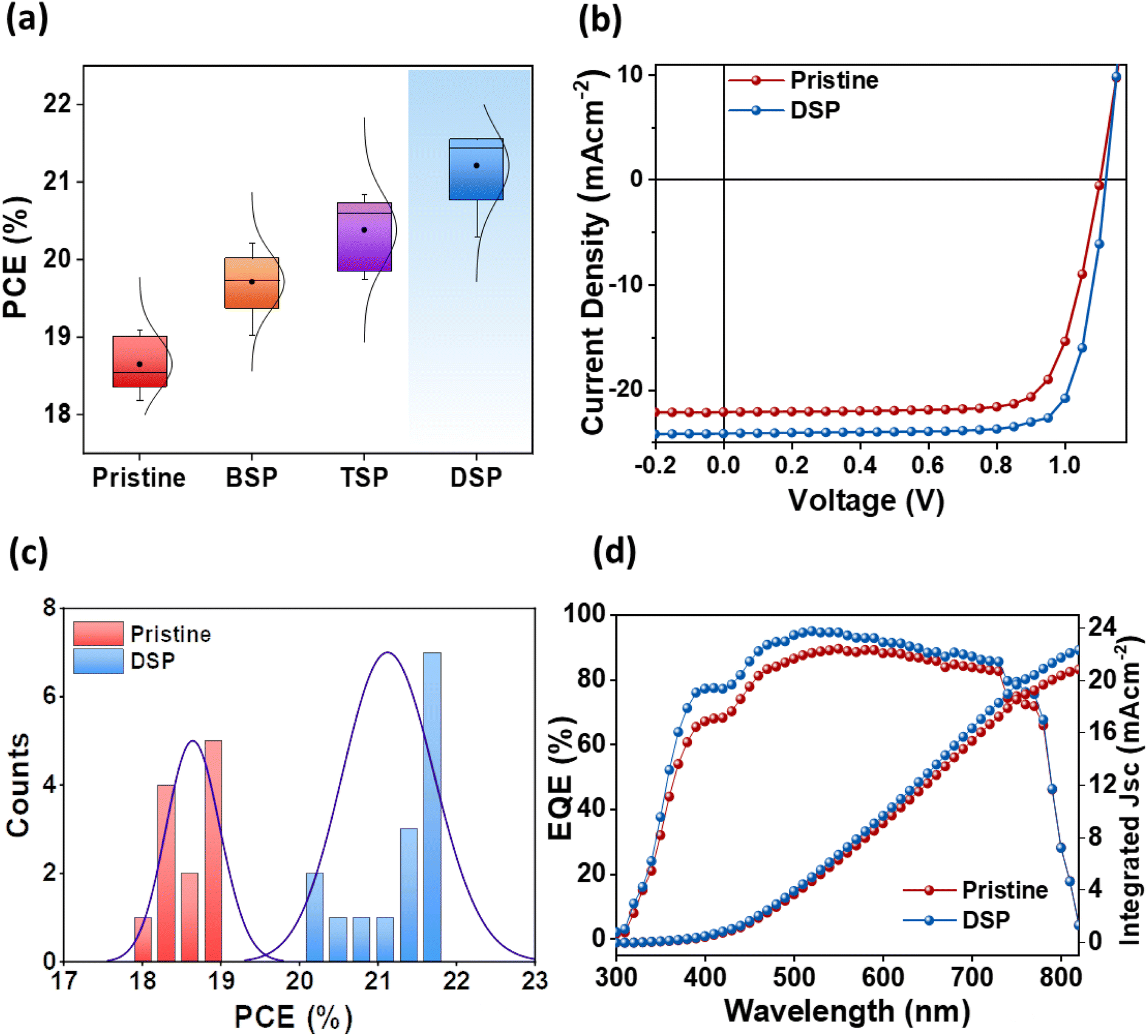 | ||
| Fig. 5 (a) Statistical analysis of PCE for pristine, BSP, TSP and DSP devices. (b) J–V characteristics of pristine and DSP based devices. (c) Statistical histogram of PCE for pristine and DSP devices. (d) External quantum efficiency curves of the pristine and DSP based devices. | ||
The pristine devices showed PCE up to 19.08%, with a Voc of 1.06 V, Jsc of 22.63 mA cm−2, and FF of 75.18%. Meanwhile the DSP strategy-based fabricated device exhibited a notably superior Voc up to 1.12 V, Jsc of 24.20 mA cm−2, and FF of 79.49%, thus resulting in an increased PCE of 21.53%, which is an improvement of 12.84% compared to the control devices (Fig. 5b). Moreover, Voc and FF were improved more than 5%, while Jsc was improved ∼7% after DSP treatment compared to the pristine devices. Furthermore, the histogram of the PCE distribution for pristine and DSP-based devices, as summarized in Fig. 5c, showed improved values for DSP devices as compared to pristine. These photovoltaic results were confirmed through external quantum efficiency (EQE), where DSP-based devices showed a better photon-to-current conversion efficiency, implying that they have better charge-collecting ability than pristine devices for the overall spectrum (Fig. 5d).
An additional significant study of the charge carrier dynamics of the IPeSCs was performed: transient photovoltage (TPV), transient photocurrent (TPC), the dependency of Voc on the intensities of light, and SCLC measurements. The lifetime of photo-induced charge carriers can be directly monitored using TPV by measuring changes in solar cell photovoltage, while TPC enables the determination of operational-time reliant charge extraction features of photo-induced charge carriers in IPeSCs.25,52 The TPC and TPV measurements were carried out in a real-time operating process, and they were determined through a double-exponential fitting decay function. As illustrated in Fig. 6a, the TPC decay lifetime of PeSCs with DSP was found to be 0.71 μs, while that for pristine was found to be 0.26 μs. Meanwhile, the TPV decay time of DSP increased from 0.24 ms (pristine) to 0.31 ms, indicating improved charge extraction and reduced charge recombination (Fig. 6b).25 Hence, the overall increase in PeSC performance could be ascribed to excellent charge transport abilities with efficiently diminished charge carrier recombination caused by perovskite defects.
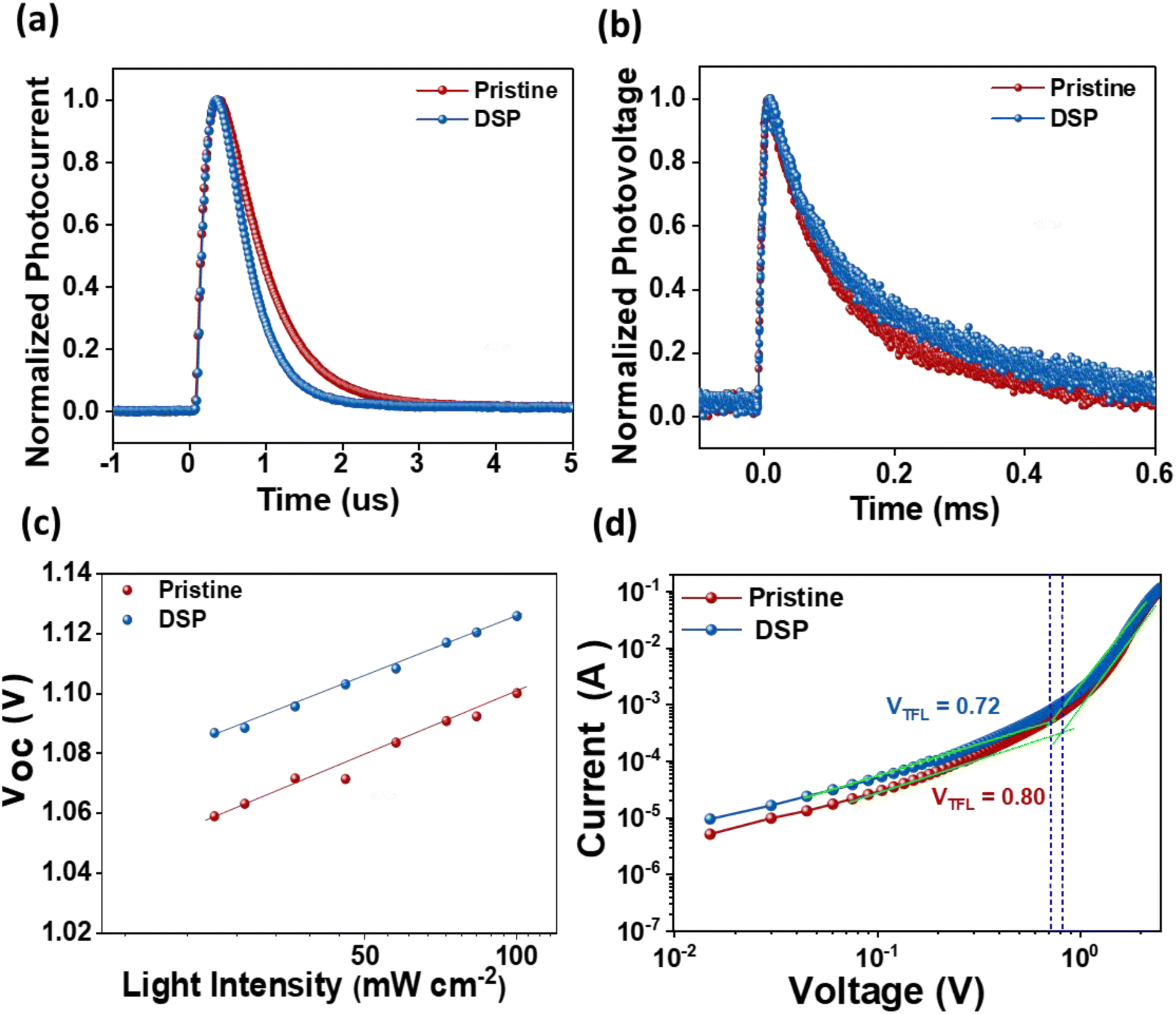 | ||
| Fig. 6 (a) Transient photocurrent (TPC) and (b) transient photovoltage (TPV) of pristine and DSP devices, (c) Vocversus light intensity of the devices for pristine and DSP devices and (d) SCLC measurements of hole-only devices for pristine and DSP devices. | ||
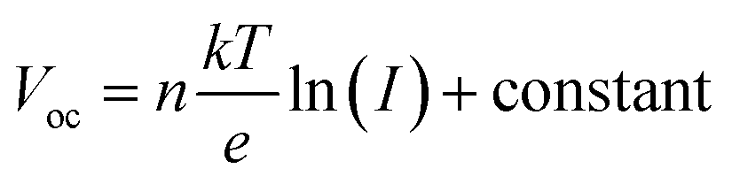
The dependency of Voc on the light intensities of the IPeScs for pristine and DSP devices is demonstrated in Fig. 6c. The degree of recombination occurring inside the perovskite solar cells was determined by using following relation:
 | (2) |
SCLC analysis was performed to confirm the defect densities in the photoactive layer film with and without passivation strategies, as exhibited in Fig. 6d. The value of VTFL was estimated to be reduced for the passivated film (0.72 V) in comparison to the pristine film (0.80 V), thus indicating that the defect densities tend to decrease with passivation. The defect densities at passivated and pristine devices were calculated to be 9.17 × 10¹⁵ and 1.02 × 10¹⁶, respectively. These results imply that the newly employed NaNO3 can enhance perovskite film-quality via better crystallinity with large size grain and significantly decreased defect densities, thereby improving the IPeSCs' overall performance.
The interfacial instability between the CTLs is an intractable obstruction to obtaining substantially efficient and long-term stable PeSCs. It is therefore necessary to address these reactions to achieve stability in PeSCs.26 To ascertain the effect of passivation on both sides, we determined operational (MPP), light, and nitrogen long-term stability for pristine and DSP unencapsulated devices. Fig. 7a shows the devices' steady-state photocurrent density measured both under continuous illumination and at their highest power point voltage under room temperature conditions of 25 ± 5 °C and 45 ± 5% relative humidity. The pristine and DSP-based devices exhibited stabilized steady-state photocurrent outputs. The DSP devices attained a steady-state photocurrent of ∼21.5 mA cm−2, whereas the pristine devices exhibited ∼17.9 mA cm−2 for 500 s. Fig. 7b shows the continuous light-soaking long-term durability of the unencapsulated device when operated under ambient conditions of 25 ± 5 °C and 45 ± 5% relative humidity. The efficiency of DSP PeSCs degraded to 50% of their original first values in 450 h, while pristine devices showed a decreasing PCE trend of approximately 10% over the same amount of time. More specifically, we observed the T80 lifetime, which is defined as the time until the photovoltaic performance of the device reduces to 80% of its first value, which is 72 h and 270 h in pristine and DSP IPeSCs, respectively, thus indicating that DSP IPeSCs demonstrate excellent long-term durability. This was proven once more by the outstanding long-term stability of DSP IPeSCs in a nitrogen environment (Fig. 7c). The DSP PeSC exhibited 76% stability for more than 1800 h, while the pristine degraded to 49% for the same amount of time. Moreover, the DSP devices maintained a T80 of ∼1582 h, compared to pristine, which maintained a T80 of 648 h. Furthermore, the T80 for BSP and TSP was measured to be 793 and 1081 h respectively (Fig. S8†). These results again signify that the DSP passivation could effectively boost the device stability. We speculate that the improvements in both light soaking and illumination stability could be associated with the improved perovskite crystallinity, with large grains, reduced grain boundary density, and an improved passivation effect from both ETL and HTL sides by DSP treatment.14 To assess the occurrence of the chemical reactions at the interfaces, we conducted XRD analysis of the aged devices after 30 days, with the results shown in Fig. 7d. The XRD peak demonstrated a PbI2 peak at 12.8° for pristine, with a slight decreasing trend in the peak intensity of the main perovskite facets, unlike the DSP films. These results explicitly suggest that the unbound Pb2+ ions were bonded successfully, as shown in eqn (1), and that ultimately, sodium nitrate could effectively passivate the defects from the bottom and top sides, thus increasing the DSP outcomes.
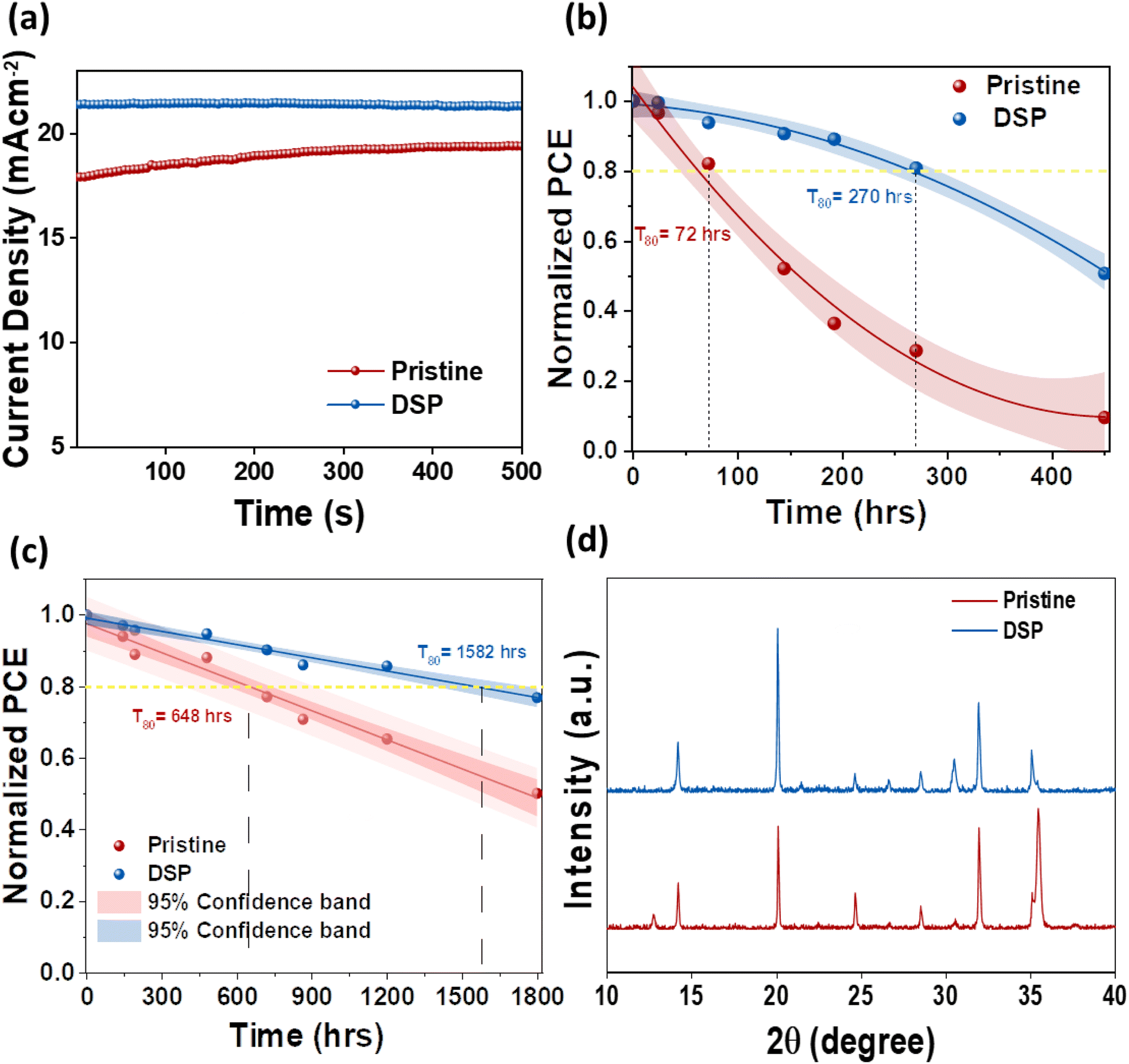 | ||
| Fig. 7 (a) Steady-state photocurrent and PCE of pristine and DSP devices. (b) Light soaking stability of pristine and DSP devices. (c) Normalized PCE as a function of time for the unencapsulated devices stored in the nitrogen environment for the PSC with pristine and DSP. (d) XRD analysis for the degraded samples for pristine and DSP devices. | ||
3. Conclusions
In this overview, we have successfully developed a π-conjugated oxysalt-assisted dual-interface engineering strategy using NaNO3 ionic solution, and we have also investigated the effect of each perovskite interface modification. The synergistic effect of Na+ and NO3− simultaneously addressed both the surface and bulk defect issues. To elaborate, the Na+ ions could interact at the NiO surface, while bonding with I/Br defects from the perovskite surface. Moreover, the passivated NiO surface can promote the growth of perovskite with improved uniform large grain and crystallinity. At the perovskite/ETL interface, we speculate that Na+ ions diffused inside the perovskite, thus resulting in reduced trap-density, while NO3− was coordinated with Pb2+, in turn leading to the formation of Pb(NO3)2, and eventually fine-tunning the alignment energy level and enlarging the device stability. These changes resulted in enhanced charge extraction and transportation at both interfaces of the perovskite. Therefore, the DSP devices showed a champion efficiency of 21.53%, surpassing those of BSP (20.16%), TSP (20.83%), and pristine (19.08%) devices. The devices also retained more than 80% stability for more than 1700 h in nitrogen for unencapsulated devices. This work paves the way to minimizing the bulk and interface non-radiative recombination losses, thus leading to simultaneous enhancement in PCE and stability through cation and anion synergistic engineering.Author contributions
Conceptualization: P. P. and S.-N. K.; methodology: P. P.; validation: P. P. and S.-I. N.; formal analysis: P. P., S. S. and D. S. M.; investigation: P. P. and S. S.; writing – original draft: P. P.; writing – review and editing: S.-I. N.; visualization: P. P.; supervision: S.-I. N.; project administration: S.-N. K. and S.-I. N.; funding acquisition: S.-N. K. and S.-I. N.Conflicts of interest
The authors declare no conflict of interest.Acknowledgements
This research was supported by the Basic Science Research Program through the National Research Foundation of Korea (NRF) funded by the Ministry of Education (RS-2023-00246239 and RS-2023-00207836) and the Open R&D Program of Korea Electric Power Corporation (R23XH02).References
- G. Hodes, Science, 2013, 342, 317–318 CrossRef CAS PubMed.
- N. J. Jeon, J. H. Noh, W. S. Yang, Y. C. Kim, S. Ryu, J. Seo and S. I. Seok, Nature, 2015, 517, 476–480 CrossRef CAS PubMed.
- G. Xing, N. Mathews, S. Sun, S. S. Lim, Y. M. Lam, M. Grätzel, S. Mhaisalkar and T. C. Sum, Science, 2013, 342, 344–347 CrossRef CAS PubMed.
- C. Li, Y. Zhang, X. Zhang, P. Zhang, X. Yang and H. Chen, Adv. Funct. Mater., 2023, 33, 2214774 CrossRef CAS.
- M. Degani, Q. An, M. Albaladejo-Siguan, Y. J. Hofstetter, C. Cho, F. Paulus, G. Grancini and Y. Vaynzof, Sci. Adv., 2021, 7, eabj7930 CrossRef CAS.
- Y.-J. Kang, S.-N. Kwon, S.-P. Cho, Y.-H. Seo, M.-J. Choi, S.-S. Kim and S.-I. Na, ACS Energy Lett., 2020, 5, 2535–2545 CrossRef CAS.
- S. Gharibzadeh, P. Fassl, I. M. Hossain, P. Rohrbeck, M. Frericks, M. Schmidt, M. R. Khan, T. Abzieher, B. A. Nejand and F. Schackmar, Energy Environ. Sci., 2021, 14, 5875–5893 RSC.
- F. Li, X. Deng, F. Qi, Z. Li, D. Liu, D. Shen, M. Qin, S. Wu, F. Lin and S.-H. Jang, J. Am. Chem. Soc., 2020, 142, 20134–20142 CrossRef CAS PubMed.
- P. Patil, D. S. Mann, U. T. Nakate, Y.-B. Hahn, S.-N. Kwon and S.-I. Na, Chem. Eng. J., 2020, 397, 125504 CrossRef CAS.
- D. S. Mann, P. Patil, D.-H. Kim, S.-N. Kwon and S.-I. Na, J. Power Sources, 2020, 477, 228738 CrossRef CAS.
- Y.-J. Kang and S.-I. Na, Nano Energy, 2022, 97, 107193 CrossRef CAS.
- S.-P. Cho, H.-J. Lee, Y.-J. Kang, Y.-H. Seo and S.-I. Na, Appl. Surf. Sci., 2022, 602, 154248 CrossRef CAS.
- S. Thakur, S.-N. Kwon, D. S. Mann and S.-I. Na, J Mater., 2022, 8, 1165–1171 Search PubMed.
- P. Patil, D. S. Mann, S. R. Rondiya, N. Y. Dzade, S.-N. Kwon and S.-I. Na, Sol. RRL, 2021, 5, 2100547 CrossRef CAS.
- S. S. Mali, J. V. Patil, J. A. Steele, Y. H. Jung, M. K. Nazeeruddin and C. K. Hong, Mater. Today, 2023, 33–45 CrossRef CAS.
- S.-M. Bang, S. S. Shin, N. J. Jeon, Y. Y. Kim, G. Kim, T.-Y. Yang and J. Seo, ACS Energy Lett., 2020, 5, 1198–1205 CrossRef CAS.
- M. Yang, G. Han, Y. Xiao and W. Hou, Chem. Commun., 2022, 58, 5638–5641 RSC.
- S. Zhang, X. Yan, Z. Liu, H. Zhu, Z. Yang, Y. Huang, S. Liu, D. Wu, M. Pan and W. Chen, J. Energy Chem., 2021, 54, 493–500 CrossRef CAS.
- T. Bu, X. Liu, Y. Zhou, J. Yi, X. Huang, L. Luo, J. Xiao, Z. Ku, Y. Peng and F. Huang, Energy Environ. Sci., 2017, 10, 2509–2515 RSC.
- H. Si, C. Xu, Y. Ou, G. Zhang, W. Fan, Z. Xiong, A. Kausar, Q. Liao, Z. Zhang and A. Sattar, Nano Energy, 2020, 68, 104320 CrossRef CAS.
- D.-Y. Son, S.-G. Kim, J.-Y. Seo, S.-H. Lee, H. Shin, D. Lee and N.-G. Park, J. Am. Chem. Soc., 2018, 140, 1358–1364 CrossRef CAS PubMed.
- C. Zhang, H. Wang, H. Li, Q. Zhuang, C. Gong, X. Hu, W. Cai, S. Zhao, J. Chen and Z. Zang, J. Energy Chem., 2021, 63, 452–460 CrossRef CAS.
- W. Fan, Y. Shen, K. Deng, Q. Chen, Y. Bai and L. Li, Nano Energy, 2022, 100, 107518 CrossRef CAS.
- W. Chen, Y. Zhou, G. Chen, Y. Wu, B. Tu, F. Z. Liu, L. Huang, A. M. C. Ng, A. B. Djurišić and Z. He, Adv. Energy Mater., 2019, 9, 1803872 CrossRef.
- Y. Guo, H. Lei, L. Xiong, B. Li and G. Fang, J. Mater. Chem. A, 2018, 6, 2157–2165 RSC.
- J. Zhang, J. Yang, R. Dai, W. Sheng, Y. Su, Y. Zhong, X. Li, L. Tan and Y. Chen, Adv. Energy Mater., 2022, 12, 2103674 CrossRef CAS.
- S. Zhang, S. Wu, R. Chen, W. Chen, Y. Huang, H. Zhu, Z. Yang and W. Chen, J. Phys. Chem. Lett., 2019, 10, 2898–2903 CrossRef CAS PubMed.
- G. Zheng, C. Zhu, J. Ma, X. Zhang, G. Tang, R. Li, Y. Chen, L. Li, J. Hu and J. Hong, Nat. Commun., 2018, 9, 2793 CrossRef PubMed.
- Y. Tidhar, E. Edri, H. Weissman, D. Zohar, G. Hodes, D. Cahen, B. Rybtchinski and S. Kirmayer, J. Am. Chem. Soc., 2014, 136, 13249–13256 CrossRef CAS PubMed.
- X. Xu, Y. Sun, D. He, Z. Liang, G. Liu, S. Xu, Z. Li, L. Zhu and X. Pan, J. Mater. Chem. C, 2021, 9, 208–213 RSC.
- S. Zhang, S. Wu, R. Chen, W. Chen, Y. Huang, Z. Yang and W. Chen, J. Mater. Chem. C, 2020, 8, 1642–1648 RSC.
- D. Zhang, X. Zhang, T. Guo, J. Zou, Y. Zhou, J. Jin, Z. Zhu, Q. Cao, J. Zhang and Q. Tai, Small, 2023, 19, 2205604 CrossRef CAS PubMed.
- J. Huang, G. Li and Y. Yang, Adv.Mater., 2008, 20, 415–419 CrossRef CAS.
- J. Xia, J. Luo, H. Yang, F. Zhao, Z. Wan, H. A. Malik, Y. Shi, K. Han, X. Yao and C. Jia, Adv. Funct. Mater., 2020, 30, 2001418 CrossRef CAS.
- D. S. Mann, S.-N. Kwon, P. Patil and S.-I. Na, Nano Energy, 2023, 106, 108062 CrossRef CAS.
- D. Di Girolamo, N. Phung, M. Jošt, A. Al-Ashouri, G. Chistiakova, J. Li, J. A. Márquez, T. Unold, L. Korte and S. Albrecht, Adv. Mater. Interfaces, 2019, 6, 1900789 CrossRef.
- J. Ciro, D. Ramírez, M. A. Mejia Escobar, J. F. Montoya, S. Mesa, R. Betancur and F. Jaramillo, ACS Appl. Mater. Interfaces, 2017, 9, 12348–12354 CrossRef CAS PubMed.
- T. Guo, Z. Fang, Z. Zhang, Z. Deng, R. Zhao, J. Zhang, M. Shang, X. Liu, Z. Hu and Y. Zhu, J. Energy Chem., 2022, 69, 211–220 CrossRef CAS.
- S. Ahmad, R. Ma, J. Zheng, C. K. Gary Kwok, Q. Zhou, Z. Ren, J. Kim, X. He, X. Zhang and K. M. Yu, Small Methods, 2022, 6, 2200787 CrossRef CAS.
- C. Bi, Q. Wang, Y. Shao, Y. Yuan, Z. Xiao and J. Huang, Nat. Commun., 2015, 6, 1–7 Search PubMed.
- C. Bi, Q. Wang, Y. Shao, Y. Yuan, Z. Xiao and J. Huang, Nat. Commun., 2015, 6, 7747 CrossRef CAS PubMed.
- K. M. Reza, A. Gurung, B. Bahrami, S. Mabrouk, H. Elbohy, R. Pathak, K. Chen, A. H. Chowdhury, M. T. Rahman and S. Letourneau, J. Energy Chem., 2020, 44, 41–50 CrossRef.
- T. Bu, J. Li, F. Zheng, W. Chen, X. Wen, Z. Ku, Y. Peng, J. Zhong, Y.-B. Cheng and F. Huang, Nat. Commun., 2018, 9, 4609 CrossRef PubMed.
- D. J. Kubicki, D. Prochowicz, A. Hofstetter, S. M. Zakeeruddin, M. Grätzel and L. Emsley, J. Am. Chem. Soc., 2018, 140, 7232–7238 CrossRef CAS PubMed.
- M.-J. Choi, Y.-S. Lee, I. H. Cho, S. S. Kim, D.-H. Kim, S.-N. Kwon and S.-I. Na, Nano Energy, 2020, 71, 104639 CrossRef CAS.
- P. Patil, A. Maibam, S. S. Sangale, D. S. Mann, H.-J. Lee, S. Krishnamurty, S.-N. Kwon and S.-I. Na, ACS Appl. Mater. Interfaces, 2023, 29597–29608 CrossRef CAS PubMed.
- S. Ding, S. Li, Q. Sun, Y. Wu, Y. Liu, Z. Li, Y. Cui, H. Wang, Y. Hao and Y. Wu, J. Mater. Chem. C, 2019, 7, 5686–5694 RSC.
- J. Yang, Q. Hong, Z. Yuan, R. Xu, X. Guo, S. Xiong, X. Liu, S. Braun, Y. Li and J. Tang, Adv. Opt. Mater., 2018, 6, 1800262 CrossRef.
- K. Hills-Kimball, Y. Nagaoka, C. Cao, E. Chaykovsky and O. Chen, J. Mater. Chem. C, 2017, 5, 5680–5684 RSC.
- M. A. Mahmud, T. Duong, Y. Yin, H. T. Pham, D. Walter, J. Peng, Y. Wu, L. Li, H. Shen and N. Wu, Adv. Funct. Mater., 2020, 30, 1907962 CrossRef CAS.
- D. V. Shinde, L. Pyeon, M. Pei, G.-W. Kim, H. Yang and T. Park, ACS Appl. Mater. Interfaces, 2017, 9, 14023–14030 CrossRef CAS PubMed.
- C. R. McNeill, I. Hwang and N. C. Greenham, J. Appl. Phys., 2009, 106, 024507 CrossRef.
- Y. Yang, H. Peng, C. Liu, Z. Arain, Y. Ding, S. Ma, X. Liu, T. Hayat, A. Alsaedi and S. Dai, J. Mater. Chem. A, 2019, 7, 6450–6458 RSC.
- Y. Huang, S. Wu, R. Chen, S. Fang, S. Zhang, G. Wang and W. Chen, ACS Appl. Mater. Interfaces, 2019, 11, 18415–18422 CrossRef CAS PubMed.
Footnote |
| † Electronic supplementary information (ESI) available: Experimental procedures/materials information can be found. See DOI: https://doi.org/10.1039/d3ta05876j |
| This journal is © The Royal Society of Chemistry 2023 |