
Charge transfer enhancement at the CZTS photocathode interface using ITO for efficient solar water reduction†
Ying Fan
Tay
a,
Mengyuan
Zhang
b,
Shuo
Zhang
b,
Stener
Lie
 b,
Sing Yang
Chiam
c and
Lydia Helena
Wong
*b
b,
Sing Yang
Chiam
c and
Lydia Helena
Wong
*b
aInstitute of Sustainability for Chemicals, Energy and Environment, A*STAR (Agency for Science, Technology and Research), 138635, Singapore
bSchool of Materials Science & Engineering, Nanyang Technological University, 50 Nanyang Ave, 639798, Singapore. E-mail: lydiawong@ntu.edu.sg
cInstitute of Materials Research and Engineering, A*STAR (Agency for Science, Technology and Research), 138635, Singapore
First published on 30th November 2023
Abstract
Cu2ZnSnS4 (CZTS) is considered as one of the most promising photocathodes for photoelectrochemical (PEC) water splitting due to its suitable optoelectronic properties. However, its PEC performance and stability degrade due to the poor interface between buffer layer CdS and catalyst Pt. In this work, indium tin oxide (ITO) was investigated as a charge transfer and protective layer for the CZTS/CdS/Pt photocathode. The solution-processed CZTS thin film coated with a CdS/ITO double layer and Pt catalyst (CZTS/CdS/ITO/Pt) yielded a photocurrent of 29 mA cm−2 at 0 VRHE and an onset potential of 0.75 VRHE, which is significantly higher than that of the pristine CZTS/CdS/Pt photocathode. More importantly, the addition of the ITO layer was found to have a “recovery” effect that enables the CZTS/CdS/ITO/Pt photocathode to remain stable under photo-reducing conditions, as confirmed by dark linear sweep voltammetry runs after a stability test. Our results suggest that the improved photocurrent, onset potential, and recovery effect are probably attributed to the removal of phosphate ions adhering to the surface of the ITO layer and higher catalytic activity at the semiconductor/electrolyte surface by forming In–Pt and Sn–Pt interactions due to partial reduction of In and Sn on the ITO surface.
1. Introduction
The use of hydrogen as an energy carrier is seen as a potential solution to our current environmental issues owing to its clean nature, which does not release any carbon-related compounds upon combustion. However, to be a truly clean energy source, hydrogen must also be produced economically and in an environmentally friendly way. Photoelectrochemical water splitting, which uses naturally abundant water and solar energy to produce hydrogen and oxygen without releasing harmful side products, has been receiving much attention since its first discovery in 1972.1 A total of 1.23 V is required to thermodynamically split water which is increased further when considering the kinetics and entropy change to convert water into gas. By separating the water splitting reaction (reduction and oxidation) using two different semiconductors (photocathode and photoanode) in tandem to carry out the respective reactions, the photovoltage required for water splitting can be divided between two materials and allow higher current densities, attaining solar-to-hydrogen conversion efficiencies of over 20%.2In terms of photocathodes, the material must have its conduction band minimum (CBM) positioned more cathodic than the water reduction potential to ensure photoelectrons have sufficient potential to reduce water and also p-type such that it produces electrons as minority carriers upon light irradiation.3 Many semiconductors have been investigated as absorber materials, such as p-Si,4,5 InP,6 GaP,7 Cu2O,8,9 Sb2Se3,10 and various copper-based chalcogenides materials such as CuInGaSe2 (CIGSe),11,12 CuInGaS2 (CIGS),13 Cu2ZnSnS4 (CZTS),14–17 CuGa3Se5,18,19 CuInS2,20,21 and Cu2BaSn (S, Se)4.22 Among them, CZTS has been regarded as a promising photocathode absorber due to its appropriate band edges with respect to the water reduction potential, a suitable band gap of around 1.5–1.6 eV which is capable of producing high current densities with sufficient overpotential to drive the water reduction reaction at higher onset potentials, and a good absorption coefficient.23 However, despite initially achieving a photocurrent of 9 mA cm−2 in its first application as a photocathode in 2010 by Yokoyama et al.,14 improvements in CZTS photocathodes have been limited. Most reported CZTS photocathodes in the literature exhibit onset potentials in the range of 0.6–0.7 VRHE and photocurrent below 20 mA cm−2.24 Furthermore, there have been no practical large-scale applications of CZTS”. This is largely due to two major factors: the stability of the photocathode in the electrolyte and the low photocurrent and onset potential.
The issue of stability has been a concern for photoelectrochemical configurations that interface semiconductors with electrolytes directly, mainly due to the requirement of a high ionic strength electrolyte for better charge conductivity.25,26 Additionally, the formation of a buried pn-junction for better charge separation necessitates an additional n-type buffer layer, further complicating the stability issue.14 According to a review by Bae et al., which evaluates most of the stability studies done on photocathodes, many of these photocathode stacks suffer from degradation under constant illumination, even at high reducing potentials of 0 VRHE.27 To address the stability issue, most photocathodes require a secondary protection layer to demonstrate hours of stability. Metal oxides such as TiO2,4,8,28–30 Al2O3,5,31 Nb2O5,32 HfO2,33,34 Ta2O5,35 RuO2,36,37 and WO3,38 sulphides such as In2S3,17 MoS2,39 and ZnS,15 metals such as Ti/Mo,40 Ti/Ni,41 and reduced graphene oxide42 have been used as protective layers. However, even with these protective layers, many still experience some form of degradation after the stability test. Furthermore, different stability results were reported even within similar protective layers.
In the case of copper chalcogenides, they are susceptible to self-oxidation of the n-type CdS layer caused by photogenerated holes and hydroxyl radicals,43,44 making it necessary to use overlayers to protect the photocathode stack. Most of the studies on CIGS and CZTS focus on using chemically inert layers such as TiO2, In2S3, and ZnS to prevent direct contact between CdS and the electrolyte. These overlayers serve to shield the corrosion-prone CdS layer and promote electron transport by introducing a secondary band bending as a type 2 heterojunction. Kumagi et al. also reported the use of Ti/Mo overlayers, which take advantage of the good electrical conductivity of the metal layers to promote electron transport while still protecting the CdS layer from the electrolyte.40 However, the performance of such photocathodes can also degrade due to the delamination of the Pt catalyst caused by poor adhesion, as reported by Koo et al. and our previous work.42,45 Therefore, overlayers must also provide good adhesion with the catalyst to maintain the catalytic activity of the photocathode stack.
In the field of the oxygen reduction reaction (ORR) in fuel cells, such catalyst binder overlayers are widely investigated. Various layers, such as aluminium zinc oxide (AZO), antimony-doped tin oxide (ATO), and indium tin oxide (ITO) have demonstrated good performance in this regard.46–48 Recently, Koo et al. utilized reduced graphene oxide as a conductive catalyst binder overlayer for photoelectrochemical cells used in water splitting and showed enhanced performance and stability of the CIGSe/CdS/rGO/Pt photocathode stack.42 ITO has also been studied as a catalyst binder for Pt in the ORR, showing improved onset potential and stability compared to carbon.46,49 Moreover, ITO has shown good electrical conductivity and transparency in the field of photovoltaics,50,51 making it an attractive material for utilization as an overlayer for the hydrogen evolution reaction (HER) photocathodes. This is in addition to its potential multifunctionality, serving as a protective layer for CdS, a charge transport layer, a catalyst binder, and an enhancer of catalyst activity. Therefore, in this study, we deposited an ITO conducting layer on top of our CZTS/CdS photocathode and subsequently Pt catalyst, demonstrating a significant increase in photocurrent and onset potential when compared to our pristine CZTS/CdS/Pt photocathode. We also suggested the formation of In–Pt and Sn–Pt bonds after Pt deposition based on X-ray photoelectron spectroscopy (XPS), which may explain the increase in catalytic activity and hence the performance of our photocathode. Our ITO layer was also effective in protecting and binding the Pt catalyst, as there was no degradation of photocurrent after an 8-hour stability test.
2. Experimental results
2.1. Fabrication of the photocathode device stack
A precursor sol solution was prepared by dissolving CuCl2·H2O (0.36 mol L−1), ZnCl2·2H2O (0.25 mol L−1), SnCl2·2H2O (0.2 mol L−1), and SC(NH2)2 (1.83 mol L−1) in 2-methoxyethanol and stirred at 50 °C in a water bath for 2 hours to obtain a dark yellow solution. All precursors were purchased from Sigma-Aldrich Company with 99% purity. The ratio of Cu/(Zn + Sn) was adjusted to about 0.86 and Zn/Sn to 1.25 following a Cu-poor, Zn-rich composition. The prepared sol solution was spin-coated on molybdenum glass substrates at 3000 rpm for 30 s followed by preheating at 280 °C for 4 min on a hot plate in air. The spin coating was repeated 12 times to obtain the desired thickness. The precursor films were then annealed at 600 °C for 40 min in a sulphur atmosphere.Following that, CdS was deposited on the CZTS thin film using the chemical bath method. The solution contains 0.025 mol L−1 of Cd(CH3COO)2, 0.375 mol L−1 of SC(NH2)2, and 8 mol L−1 NH4OH at 60 °C for 14 min. Indium tin oxide (ITO) was sputtered at room temperature with Ar pressure for 7 min at a sputtering power of 75 W. Lastly, Pt was deposited through photoelectrodeposition (PED) with an electrolyte of pH 9.5. Na2SO4 was used, and 200 μl of 1 mg Pt per ml H2PtCl6 was added to the electrolyte.
2.2. Characterization
PEC measurements were conducted on a CHI 660D workstation (CH Instruments Inc.) using a three-electrode setup with a solar simulator (PEC-L01, Peccell) applying AM 1.5G irradiation at 100 mW cm−2 as the light source. A Pt wire and Ag/AgCl in 3 M saturated KCl aqueous solution were employed as counter and reference electrodes, respectively.The X-ray diffraction data and scanning electron microscopy (SEM) of the thin films were performed using a Bruker D8 Advance and FESEM (JEOL, JSM-7600F).
The electrochemical impedance spectroscopy (EIS) (Nyquist and corresponding Bode plots) and Mott–Schottky measurements were conducted using an electrochemical workstation (Autolab PGSTAT302N). The amplitude of the sinusoidal wave was 0 mV, and the frequency range was from 100 kHz to 0.1 Hz. EIS spectra were further analysed with the Nova software package.
XPS measurements were carried out using a VG ESCALAB2201-XL instrument under a base pressure of <5 × 10¹⁰ mbar and equipped with a monochromatic Al Kα (1486.7 eV) X-ray source and a He I discharge lamp (21.2 eV) UV source.
The faradaic efficiency measurement was conducted using a PEC cell connected to an online gas chromatography system (Agilent 490 Micro GC gas analyzer equipped with an MS-5A column and a thermal conductivity detector) to detect H2 and O2 during PEC water splitting.
Transmission electron microscopy (TEM) analysis was performed using a JEOL 2010UHR transmission electron microscope with a 1k × 1k Gatan 794 MSC CCD camera.
3. Results and discussion
Fig. 1a shows the current density–potential curve of CZTS/CdS/Pt and CZTS/CdS/ITO/Pt photocathodes under chopped illumination of simulated sunlight (AM 1.5G). A significant enhancement of photocurrent from 15 mA cm−2 to 29 mA cm−2 was achieved when an ITO overlayer was introduced between CdS and the Pt catalyst. The CZTS in this study has a band gap of around 1.67 eV as shown from the EQE measurement (Fig. S1†). This increase in photocurrent was also observed prior to Pt deposition, where the additional ITO layer increased the photocurrent at higher onset potentials (Fig. S2†). The improved photocurrent confirms the enhanced electronic conductivity but the slow kinetics without Pt as a proper catalyst result in transients where most of the photogenerated charges recombine. It was also observed that the ITO layer increased the onset potential of the photocurrent for CZTS/CdS/ITO/Pt by about 0.16 V (from 0.59 to 0.75 VRHE), as seen from the derivative of photocurrent/potential vs. potential curve in Fig. 1b. This increase in onset potential indicates improved charge transport to the electrolyte, which could be attributed to either increased catalytic activity at the surface or enhanced electronic transport to the catalyst. In Fig. 1c and d, the current density–potential curves for CZTS/CdS/Pt and CZTS/CdS/ITO/Pt are shown, with both forward (anodic direction) and reverse (cathodic direction) superimposed on the same graph. It can be observed that without the ITO overlayer (Fig. 1c), CZTS/CdS/Pt suffers from severe hysteresis, where the onset potential, photocurrent at 0 VRHE, and the shape of the curve change drastically for different scan directions. The hysteresis cannot be recovered by repeating the forward and reverse measurements at different scan rates of 0.005, 0.01, and 0.02 V s−1 (Fig. S3†), suggesting that the charge trapping process time constant is slower than the scan rate. The literature offers different explanations for such hysteresis, such as photochemical stability,52 transient pH shifts within the pores of the photocathode,53 and negative charge trapping/de-trapping at interfaces.54,55 In our study, we hypothesize that there is a capacitive build-up at the CdS/Pt interface, possibly due to charged trap states where Pt grows on CdS since the bottom layers are similar. With the ITO overlayer, the interaction between ITO and Pt may reduce the amount of charge traps in this layer and reduce the hysteresis.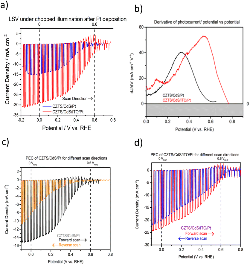 | ||
| Fig. 1 (a) Current density–potential curves of CZTS/CdS/Pt and optimized CZTS/CdS/ITO/Pt in 1 M K2HPO4/KH2PO4 solution (pH 7) under chopped solar-simulated AM 1.5G light irradiation. (b) Corresponding derivative of photocurrent/potential vs. potential curves for CZTS/CdS/Pt and CZTS/CdS/ITO/Pt in the same electrolyte. (c) Current density–potential curves of CZTS/CdS/Pt in the same electrolyte under similar testing conditions for different scan directions (forward: negative to positive and reverse: positive to negative) at a scan rate of 0.01 V s−1. (d) Corresponding current density–potential curves for CZTS/CdS/ITO/Pt. | ||
In order to support and further elaborate on our hypothesis about the ITO and Pt interaction, we performed XPS, TEM, and impedance spectroscopy. The XPS spectra include the In 3d fitted peaks for CZTS/CdS/ITO before and after Pt (CZTS/CdS/ITO/Pt) and the Pt 4f peak for CZTS/CdS/ITO/Pt and CZTS/CdS/Pt, as shown in Fig. 2a and b separately. The XPS spectra are normalized to the total area to allow easy comparison between peak positions. For CZTS/CdS/ITO, the In 3d is fitted with three components, 443.93 eV, 444.77 eV, and 445.35 eV. The first two components are assigned to indium oxide (In2O3) and indium hydroxide, while the last component is unassigned and may be due to surface contaminants.56 For CZTS/CdS/ITO/Pt, a clear shoulder at a lower binding energy is observed, and three components are used to fit the spectra with binding energies of 443.12 eV, 443.97 eV, and 444.77 eV. The last two components (443.97 eV and 444.77 eV) are assigned to indium oxide and indium hydroxide, similarly to that of CZTS/CdS/ITO. However, the first component at 443.12 eV is not detected for CZTS/CdS/ITO, indicating a new chemical environment that is less electron-withdrawing forming around In when Pt is photoelectrodeposited on ITO. The full width at half maximum of this new component is also smaller than those assigned to In2O3 (0.8 eV vs. 1.2 eV) which suggests that the new phase of In is more metallic based on earlier reports.56 A similar lower binding energy shoulder is also observed in the Sn 3d spectra after Pt deposition (Fig. S4†), which suggests that it may be the partially reduced metallic Sn. The O1s XPS spectra are fitted with four components: 529.42 eV, 530.45 eV, 531.32 eV, and 532.14 eV (Fig. S5†). The first two components (529.42 eV and 530.45 eV) are assigned to oxygen in the In2O3 lattice, with the higher binding energy component corresponding to oxygen adjacent to oxygen-deficient positions. For the other two components (531.32 eV and 532.14 eV), the lower binding energy component is assigned to surface hydroxide or oxyhydroxide, while the other is due to oxygen contaminants.56 A significant drop in lattice O in In2O3 is observed after Pt photoelectrodeposition, suggesting that oxygen is lost when Pt interacts with In. These observations were not observed in our control experiment where Pt was sputtered instead of photoelectrodeposited (Fig. S6†).
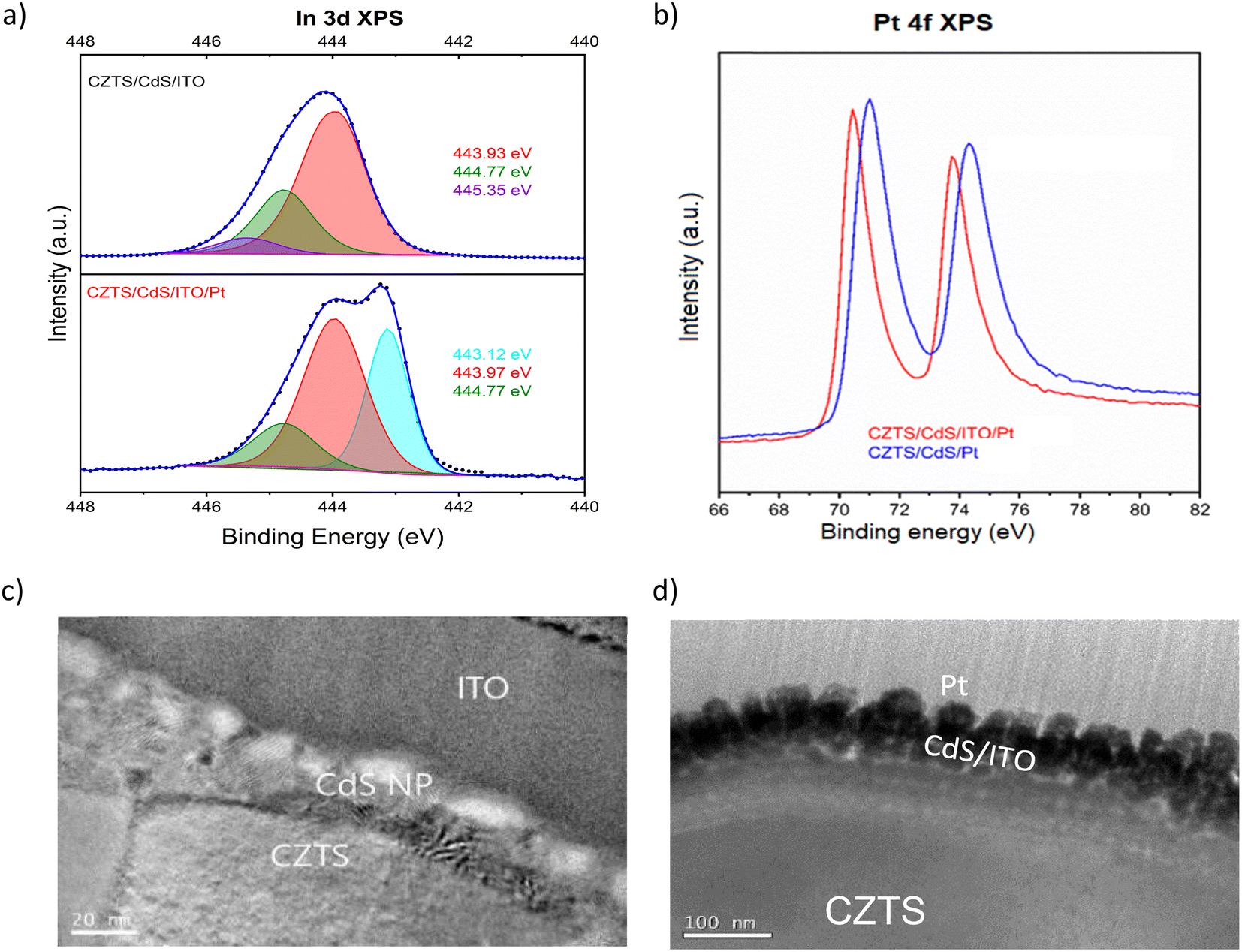 | ||
| Fig. 2 (a) In 3d XPS spectra of CZTS/CdS/ITO before (top panel) and after (bottom panel) photoelectrodeposition (PED) of Pt after normalizing the total peak area. The peaks are assigned to indium oxide (In2O3) (red), indium hydroxide (In(OH)3) (green), metallic indium (In) (blue), and unidentified surface contaminants (purple). (b) Pt 4f XPS spectra of Pt on CZTS/CdS/ITO (CZTS/CdS/ITO/Pt) and on CZTS/CdS (CZTS/CdS/Pt). (c) Bright-field STEM images of CZTS/CdS/ITO before Pt deposition. (d) HR TEM images of CZTS/CdS/ITO/Pt after Pt deposition. | ||
Based on this information, we suggest that the shifts mentioned above result from the loss of oxygen atoms which are coordinated to Indium through the formation of a bond between In and Pt (O–In–Pt). This hypothesis is supported by the Pt 4f XPS peak shifting towards lower binding energy upon the photoelectrodeposition of Pt on ITO (Fig. 2b), as compared to CdS, due to S (Cd–S–Pt) having a more pronounced withdrawing effect compared to In (O–In–Pt). Previous studies have also reported similar findings in which the activity of the ORR increased due to electron transfer between In and Pt or the alloying.57 Furthermore, the interaction between Sn and Pt has also been reported to enhance the activity of Pt for the same ORR application.46,58 In our work, we observed an increase in catalytic activity when Pt is bonded to In as compared to S, as shown by the dark current measurement in Fig. S7,† where the dark current of CZTS/CdS/ITO/Pt requires lower overpotentials to achieve higher currents compared to CZTS/CdS/Pt. This increase in catalytic activity may be due to the reported synergistic effect between In and Pt, which complements the advantages of using ITO as a charge transport layer.
Subsequently, the impact of the interaction between ITO and Pt on morphology is illustrated through TEM images of CZTS/CdS/ITO before and after Pt electrodeposition, as presented in Fig. 2c and d, respectively. Based on the STEM images in Fig. 2c and the TEM EDX line scan (Fig. S8†), the thickness of CdS grown by chemical bath deposition (CBD) is estimated to be around 20 nm, while the sputtered ITO layer is around 80 nm, with its amorphous structure observed by XRD (Fig. S9†). The atomic ratio of ITO is determined by XPS to be relatively similar to stoichiometric In2O3 with 10% Sn doping relative to In (Table S1†). After Pt photoelectrodeposition, the thickness of the ITO layer decreased to 50 nm, and an intermixing layer with Pt at the interface of approximately 20 nm was observed (Fig. 2d). In addition, Pt nanoparticles with a diameter of around 40 nm were uniformly distributed on the surface of the intermixed layer.
To gain deeper insights into the charge transfer mechanism, we constructed electrochemical impedance Nyquist plots for CZTS/CdS/Pt and CZTS/CdS/ITO/Pt at various applied potentials under AM 1.5G illumination, as depicted in Fig. 3a and b. The extracted charge transfer resistance (Rct) and capacitance are plotted against applied potential (Mott–Schottky) in Fig. 3c and d, respectively. The Mott–Schottky plot in Fig. 3d shows a similar positive slope for both CZTS/CdS/Pt and CZTS/CdS/ITO/Pt, indicating that the probing depletion region is n-type, most probably associated with the CdS layer. From the extracted Rct, we observed that with the introduction of ITO between CdS and Pt, the Rct clearly decreases by 1 to 2 orders of magnitude, indicating an improvement in charge transfer to the electrolyte, which may result from better catalytic efficiency or improved charge transport from CdS to the Pt due to the presence of the ITO layer. Furthermore, when comparing the trend of Rct with applied potential, for CZTS/CdS/ITO/Pt, the Rct decreases linearly with applied cathodic potential, which is consistent with the behavior of a photocathode. However, for CZTS/CdS/Pt, the resistance first increases to a maximum at 0.15 VRHE, then decreases to a minimum at 0 VRHE with increasing cathodic potential applied. Applying cathodic potentials should increase the depletion width and increase band bending, allowing more charges to reach the semiconductor/electrolyte junction. This suggests that there is some sort of limiting factor in CZTS/CdS/Pt that prevents charge transfer to the electrolyte in the applied potential range of 0.40 VRHE to 0.15 VRHE, hence limiting the performance of the CZTS/CdS/Pt photocathode. This is also supported by the open circuit potential measurement of CZTS/CdS/Pt and CZTS/CdS/ITO/Pt (Fig. S10†), where CZTS/CdS/Pt shows a more gradual decrease in open circuit voltage upon turning off illumination, indicating a slower release of charges from trap states. This limitation might be attributed to the presence of defect levels at the CdS/Pt interface, as supported by OCP decay and also by the current density–voltage hysteresis, which prevents the band levels of CZTS/CdS from being equilibrated with the electrolyte. This finding shed light on one of the limitations of the CZTS/CdS/Pt photocathode in the absence of an intermediate charge transport layer. Another observation is the much higher illuminated open circuit voltage of CZTS/CdS/ITO/Pt (0.4 V) compared to CZTS/CdS/Pt (0.1 V) which indicates the presence of an additional heterojunction formed between CdS and ITO. However, we observed the work function of ITO and CdS to be similar (Fig. S11†), suggesting that additional heterojunction formation should not be the reason for the improved charge transport. In addition to enhancing catalytic activity and photocathode performance, we investigated the impact of ITO on the stability of the photocathode. Fig. 4a illustrates the current–time curve of CZTS/CdS/ITO/Pt in a 1 M K2HPO4/KH2PO4 (pH 7) solution under solar-simulated AM 1.5G irradiation at an applied bias of 0 VRHE for a duration of 12 hours. The stability test was conducted at 2-hour intervals. After 2 hours of continuous light irradiation and applied bias, the light irradiation and bias were switched off, and three linear sweep voltammetry (LSV) sweeps were performed. The LSV was conducted in the anodic direction from −0.2 VRHE to 0.8 VRHE under dark conditions, as shown in Fig. S12.† A change in the shape of the current density–potential curve is observed at both high potential (0.5–0.8 VRHE) and low potential (0 VRHE), as indicated by the red circles. This change may be indicative of a similar desorption process observed by Ramaker et al.59 The faradaic efficiency is close to 100% as shown in Fig. S13,† where the time–course curve for H2 production for CZTS/CdS/ITO/Pt follows close to the time–course curve for e−/2.59 Following the recovery LSV sweeps, the photocurrent was able to return to its original value, despite decreasing to 64% of its initial value after the 2-hour stability test (Fig. 4b). This recovery effect was also supported by scanning electron microscopy (SEM) images, where CZTS/CdS/ITO/Pt subjected to regular anodic LSV sweeps (Fig. 4c) appeared pristine and significantly different from a similar sample without such treatment (Fig. 4d). The sample without the recovery treatment seemed to be covered by a layer of particles, approximately 100 nm in size, after the stability test. These particles may consist of phosphate and potassium ions, as indicated by the SEM EDX results (Fig. S14†). Almost no potassium (K) and phosphorus (P) were detected for the sample subjected to the recovery LSV sweep (within the confidence margin). This suggests that the presence of K+ and PO43− on the surface may hinder the transport of electrons from Pt to the electrolyte, leading to the initial decrease in photocurrent. Furthermore, the implemented recovery LSV sweep was effective in removing this layer, implying that the adhesion of K+ and PO43− is a surface adhesion. This surface adhesion is further supported by the observation when CZTS/CdS/ITO/Pt was immersed in a K2HPO4/KH2PO4 solution overnight, exhibited a similar layer coating its surface in SEM images and a corresponding decrease in photocurrent in current density–potential curves (Fig. S15†).
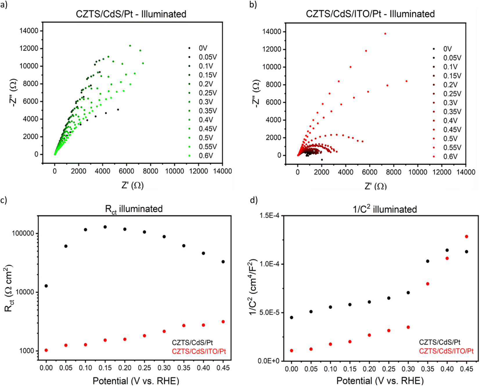 | ||
| Fig. 3 (a) Nyquist plot of CZTS/CdS/Pt photocathodes under AM 1.5G illumination in 1 M K2HPO4/KH2PO4 solution in pH 7 under different applied potentials. (b) Corresponding Nyquist plot for CZTS/CdS/ITO/Pt photocathodes tested in similar electrolytes and under similar conditions. (c) Plot of extracted charge transfer resistance (diameter of the semicircle at high frequency) vs. applied potential for CZTS/CdS/Pt and CZTS/CdS/ITO/Pt under illumination. (d) Mott–Schottky plot of extracted 1/C2vs. applied potential for the same photocathodes. | ||
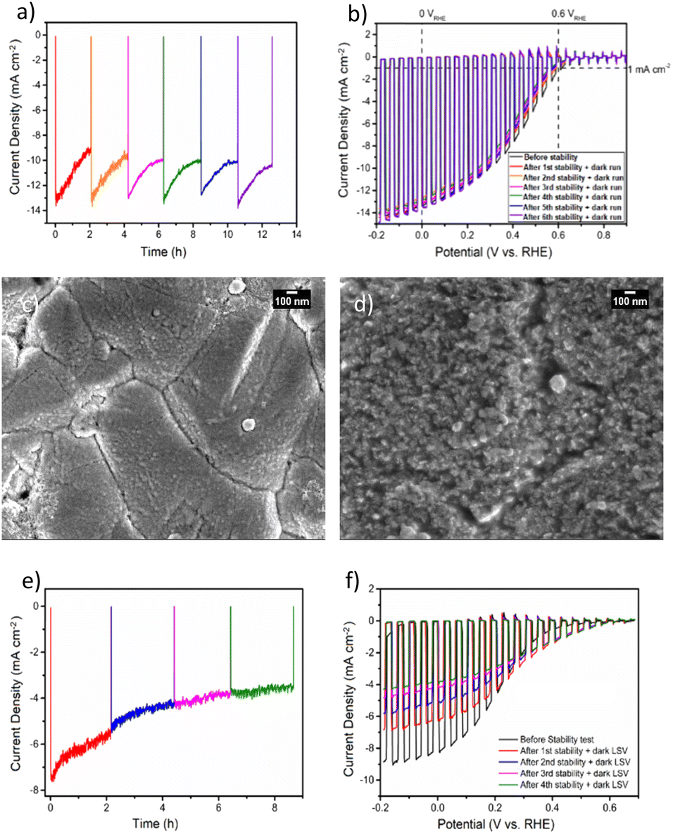 | ||
| Fig. 4 (a) Current–time curve of CZTS/CdS/ITO/Pt in 1 M K2HPO4/KH2PO4 (pH 7) under solar simulated AM 1.5G light irradiation at an applied bias of 0 VRHE. The stability test is conducted at 2 h intervals with 3 recovery dark LSV sweeps at every interval. (b) Corresponding chopped LSV before the stability test and after each recovery dark LSV sweep. Scanning electron microscopy (SEM) of CZTS/CdS/ITO/Pt after 12 h stability test (c) with recovery dark LSV (d) without recovery dark LSV sweeps. (e) Stability test and (f) corresponding LSV for the photocathode without ITO (CZTS/CdS/Pt). | ||
However, when we applied similar recovery LSV sweeps to a CZTS photocathode without the ITO layer during a similar stability test (Fig. 4e), we observed that the photocurrent could not be restored, and the overall photocurrent continued to decrease over time (Fig. 4e). Additionally, the dark LSV recovery sweep caused the maximum photocurrent at 0 VRHE to decrease further (Fig. 4f), suggesting that the degradation process of CZTS/CdS/Pt involves not only the surface adhesion of K+ and PO43− but also another mechanism that cannot be rectified through such LSV sweeps. This type of degradation induced by the phosphate buffer electrolyte has been documented for other materials, such as BiVO4,60,61 where it is attributed to dissolution, particularly under conditions of high pH, bias, and illumination. Interestingly, it has also been shown to enhance stability for materials like Fe2O3, as it prevents the accumulation of photogenerated holes on the surface of Fe2O3.62 This implies that the stability of the material in a potassium phosphate buffer is linked to the stability of the complex formed at the semiconductor/electrolyte interface. In the context of the CZTS photocathode featuring an ITO overlayer, our observations point to performance degradation during the stability test under illumination (see Fig. 4a) primarily arising from the adhesion of K+ and PO43− on the surface of ITO/Pt ions to the surface of ITO/Pt. Since dissolution processes are not involved, the impairment of photocurrent can be attributed to the physical adhesion of these ions to the surface. In contrast, for CZTS photocathodes lacking an ITO layer, after the stability test, the photocurrent does not recover to its original value when dark LSV is conducted. This phenomenon may be linked to changes in the chemical environment surrounding the CdS layer.
4. Conclusions
The ITO conducting layer between the CdS buffer layer and Pt catalyst is shown to enhance the photocurrent and onset potential of the CZTS photocathode, achieving a maximum photocurrent of 29 mA cm−2 at 0 VRHE and an onset potential of 0.75 VRHE. This increase in performance is attributed to a combination of two factors: better charge conduction from CdS to Pt due to the higher electronic conductivity of the ITO layer and improved catalytic activity at the semiconductor/electrolyte interface due to a partial reduction of In and Sn on the surface of ITO, forming In–Pt and Sn–Pt interactions. This interaction helps increase the density of electrons on the Pt surface, hence enhancing its catalytic activity. The inclusion of the ITO layer is also found to prevent the degradation of the underlying CdS and CZTS layers while anchoring the Pt catalyst, thus preventing Pt delamination. A 12-hour stability test with recovery dark LSV steps shows almost no decay in photocurrent, highlighting the promise of using ITO as a protective layer.Conflicts of interest
There are no conflicts to declare.Acknowledgements
The authors would like to acknowledge the funding support from the CREATE Programme under the Campus for Research Excellence and Technological Enterprise (CREATE), which is supported by the National Research Foundation, Prime Minister's Office, Singapore, and the Ministry of Education (MOE) Tier 2 Project (MOE-T2EP50120-0008).References
- A. Fujishima and K. Honda, Nature, 1972, 238, 37–38 CrossRef CAS PubMed.
- M. S. Prévot and K. Sivula, J. Phys. Chem. C, 2013, 117, 17879–17893 CrossRef.
- J. H. Kim, D. Hansora, P. Sharma, J.-W. Jang and J. S. Lee, Chem. Soc. Rev., 2019, 48, 1908–1971 RSC.
- J. Liang, H. Tan, M. Liu, B. Liu, N. Wang, Q. Zhang, Y. Zhao, A. H. M. Smets, M. Zeman and X. Zhang, J. Mater. Chem. A, 2016, 4, 16841–16848 RSC.
- R. Fan, W. Dong, L. Fang, F. Zheng, X. Su, S. Zou, J. Huang, X. Wang and M. Shen, Appl. Phys. Lett., 2015, 106, 013902 CrossRef.
- Y. Lin, R. Kapadia, J. Yang, M. Zheng, K. Chen, M. Hettick, X. Yin, C. Battaglia, I. D. Sharp, J. W. Ager and A. Javey, J. Phys. Chem. C, 2015, 119, 2308–2313 CrossRef CAS.
- M. Malizia, B. Seger, I. Chorkendorff and P. C. K. Vesborg, J. Mater. Chem. A, 2014, 2, 6847–6853 RSC.
- L. Pan, J. H. Kim, M. T. Mayer, M.-K. Son, A. Ummadisingu, J. S. Lee, A. Hagfeldt, J. Luo and M. Grätzel, Nat. Catal., 2018, 1, 412–420 CrossRef CAS.
- C. G. Morales-Guio, L. Liardet, M. T. Mayer, S. D. Tilley, M. Grätzel and X. Hu, Angew. Chem., Int. Ed., 2015, 54, 664–667 CrossRef CAS PubMed.
- J. Tan, B. Kang, K. Kim, D. Kang, H. Lee, S. Ma, G. Jang, H. Lee and J. Moon, Nat. Energy, 2022, 7, 537–547 CrossRef CAS.
- M. G. Mali, H. Yoon, B. N. Joshi, H. Park, S. S. Al-Deyab, D. C. Lim, S. Ahn, C. Nervi and S. S. Yoon, ACS Appl. Mater. Interfaces, 2015, 7, 21619–21625 CrossRef CAS PubMed.
- H. Kobayashi, N. Sato, M. Orita, Y. Kuang, H. Kaneko, T. Minegishi, T. Yamada and K. Domen, Energy Environ. Sci., 2018, 11, 3003–3009 RSC.
- W. Septina, Gunawan, S. Ikeda, T. Harada, M. Higashi, R. Abe and M. Matsumura, J. Phys. Chem. C, 2015, 119, 8576–8583 CrossRef CAS.
- D. Yokoyama, T. Minegishi, K. Jimbo, T. Hisatomi, G. Ma, M. Katayama, J. Kubota, H. Katagiri and K. Domen, Appl. Phys. Express, 2010, 3, 101202 CrossRef.
- K. Wang, D. Huang, L. Yu, H. Gu, S. Ikeda and F. Jiang, J. Colloid Interface Sci., 2019, 536, 9–16 CrossRef CAS PubMed.
- K. Feng, D. Huang, L. Li, K. Wang, J. Li, T. Harada, S. Ikeda and F. Jiang, Appl. Catal., B, 2019, 118438, DOI:10.1016/j.apcatb.2019.118438.
- F. Jiang, Gunawan, T. Harada, Y. Kuang, T. Minegishi, K. Domen and S. Ikeda, J. Am. Chem. Soc., 2015, 137, 13691–13697 CrossRef CAS PubMed.
- C. P. Muzzillo, W. E. Klein, Z. Li, A. D. DeAngelis, K. Horsley, K. Zhu and N. Gaillard, ACS Appl. Mater. Interfaces, 2018, 10, 19573–19579 CrossRef CAS PubMed.
- L. Zhang, T. Minegishi, M. Nakabayashi, Y. Suzuki, K. Seki, N. Shibata, J. Kubota and K. Domen, Chem. Sci., 2015, 6, 894–901 RSC.
- J. Zhao, T. Minegishi, L. Zhang, M. Zhong, Gunawan, M. Nakabayashi, G. Ma, T. Hisatomi, M. Katayama, S. Ikeda, N. Shibata, T. Yamada and K. Domen, Angew. Chem., Int. Ed., 2014, 53, 11808–11812 CrossRef CAS PubMed.
- S. Y. Chae, S. Kim and O.-S. Joo, J. Mater. Chem. A, 2019, 7, 2041–2047 RSC.
- J. Song, B. Teymur, Y. Zhou, E. Ngaboyamahina and D. B. Mitzi, ACS Appl. Energy Mater., 2021, 4, 81–87 CrossRef CAS.
- W. Yang and J. Moon, ChemSusChem, 2019, 12, 1889–1899 CrossRef CAS PubMed.
- S. Hadke, M. Huang, C. Chen, Y. F. Tay, S. Chen, J. Tang and L. Wong, Chem. Rev., 2021, 122, 10170–10265 CrossRef PubMed.
- S. Chen and L.-W. Wang, Chem. Mater., 2012, 24, 3659–3666 CrossRef CAS.
- K. Walczak, Y. Chen, C. Karp, J. W. Beeman, M. Shaner, J. Spurgeon, I. D. Sharp, X. Amashukeli, W. West, J. Jin, N. S. Lewis and C. Xiang, ChemSusChem, 2015, 8, 544–551 CrossRef CAS PubMed.
- D. Bae, B. Seger, P. C. K. Vesborg, O. Hansen and I. Chorkendorff, Chem. Soc. Rev., 2017, 46, 1933–1954 RSC.
- W. Yang, Y. Oh, J. Kim, M. J. Jeong, J. H. Park and J. Moon, ACS Energy Lett., 2016, 1, 1127–1136 CrossRef CAS.
- Y. Zhou, D. Shin, E. Ngaboyamahina, Q. Han, C. B. Parker, D. B. Mitzi and J. T. Glass, ACS Energy Lett., 2018, 3, 177–183 CrossRef CAS.
- R. Fan, W. Dong, L. Fang, F. Zheng and M. Shen, J. Mater. Chem. A, 2017, 5, 18744–18751 RSC.
- H. Xing, E. Lei, D. Zhao, X. Li, M. Ruan and Z. Liu, Chem. Commun., 2019, 55, 15093–15096 RSC.
- J. J. M. Vequizo, M. Yokoyama, M. Ichimura and A. Yamakata, Appl. Phys. Express, 2016, 9, 067101 CrossRef.
- D. Huang, K. Wang, L. Yu, T. H. Nguyen, S. Ikeda and F. Jiang, ACS Energy Lett., 2018, 3, 1875–1881 CrossRef CAS.
- D. Huang, K. Wang, L. Li, K. Feng, N. An, S. Ikeda, Y. Kuang, Y. Ng and F. Jiang, Energy Environ. Sci., 2021, 14, 1480–1489 RSC.
- T. Wang, S. Liu, H. Li, C. Li, Z. Luo and J. Gong, Ind. Eng. Chem. Res., 2019, 58, 5510–5515 CrossRef CAS.
- Y. Kageshima, T. Minegishi, S. Sugisaki, Y. Goto, H. Kaneko, M. Nakabayashi, N. Shibata and K. Domen, ACS Appl. Mater. Interfaces, 2018, 10, 44396–44402 CrossRef CAS PubMed.
- H. Kaneko, T. Minegishi, T. Higashi, M. Nakabayashi, N. Shibata and K. Domen, Small Methods, 2018, 2, 1800018 CrossRef.
- D. W. Palm, C. P. Muzzillo, M. Ben-Naim, I. Khan, N. Gaillard and T. F. Jaramillo, Sustainable Energy Fuels, 2021, 5, 384–390 RSC.
- J. Gu, J. A. Aguiar, S. Ferrere, K. X. Steirer, Y. Yan, C. Xiao, J. L. Young, M. Al-Jassim, N. R. Neale and J. A. Turner, Nat. Energy, 2017, 2, 16192 CrossRef CAS.
- H. Kumagai, T. Minegishi, N. Sato, T. Yamada, J. Kubota and K. Domen, J. Mater. Chem. A, 2015, 3, 8300–8307 RSC.
- C. Yu, Q. Jia, H. Zhang, W. Liu, X. Yu and X. Zhang, Inorg. Chem. Front., 2019, 6, 527–532 RSC.
- B. Koo, S. Byun, S.-W. Nam, S.-Y. Moon, S. Kim, J. Y. Park, B. T. Ahn and B. Shin, Adv. Funct. Mater., 2018, 28, 1705136 CrossRef.
- X.-L. Yin, J. Liu, W.-J. Jiang, X. Zhang, J.-S. Hu and L.-J. Wan, Chem. Commun., 2015, 51, 13842–13845 RSC.
- X. Chen, S. Shen, L. Guo and S. S. Mao, Chem. Rev., 2010, 110, 6503–6570 CrossRef CAS PubMed.
- Y. F. Tay, H. Kaneko, S. Y. Chiam, S. Lie, Q. Zheng, B. Wu, S. S. Hadke, Z. Su, P. S. Bassi, D. Bishop, T. C. Sum, T. Minegishi, J. Barber, K. Domen and L. H. Wong, Joule, 2018, 2, 537–548 CrossRef CAS.
- Y. Liu and W. E. Mustain, J. Am. Chem. Soc., 2013, 135, 530–533 CrossRef CAS PubMed.
- G. Cognard, G. Ozouf, C. Beauger, G. Berthomé, D. Riassetto, L. Dubau, R. Chattot, M. Chatenet and F. Maillard, Appl. Catal., B, 2017, 201, 381–390 CrossRef CAS.
- Y. Gao, M. Hou, Z. Shao, C. Zhang, X. Qin and B. Yi, RSC Adv., 2015, 5, 69479–69486 RSC.
- Y. Liu and W. E. Mustain, ECS Trans., 2013, 53, 1–6 CrossRef.
- H.-S. Im, S.-K. Kim, T.-J. Lee and T.-Y. Seong, Vacuum, 2019, 169, 108871 CrossRef CAS.
- R. M. Pasquarelli, D. S. Ginley and R. O'Hayre, Chem. Soc. Rev., 2011, 40, 5406–5441 RSC.
- K. Sun, K. Madsen, P. Andersen, W. Bao, Z. Sun and D. Wang, Nanotechnology, 2012, 23, 194013 CrossRef PubMed.
- L. Tong, A. Iwase, A. Nattestad, U. Bach, M. Weidelener, G. Götz, A. Mishra, P. Bäuerle, R. Amal, G. G. Wallace and A. J. Mozer, Energy Environ. Sci., 2012, 5, 9472–9475 RSC.
- R. C. Valderrama, P. J. Sebastian, J. Pantoja Enriquez and S. A. Gamboa, Sol. Energy Mater. Sol. Cells, 2005, 88, 145–155 CrossRef CAS.
- J.-Y. Jung, D. Woong Kim, D.-H. Kim, T. Joo Park, R. B. Wehrspohn and J.-H. Lee, Sci. Rep., 2019, 9, 9132 CrossRef PubMed.
- C. Donley, D. Dunphy, D. Paine, C. Carter, K. Nebesny, P. Lee, D. Alloway and N. R. Armstrong, Langmuir, 2002, 18, 450–457 CrossRef CAS.
- Y. Cheng, X. Zhao, Y. Yu, L. Chen, T. Cheng, J. Huang, Y. Liu, M. Harada, A. Ishihara and Y. Wang, J. Power Sources, 2020, 446, 227332 CrossRef CAS.
- K. Zhang, H. Dong, W. Dai, X. Meng, H. Lu, T. Wu and X. Zhang, Anal. Chem., 2017, 89, 648–655 CrossRef CAS PubMed.
- D. E. Ramaker, D. Gatewood, A. Korovina, Y. Garsany and K. E. Swider-Lyons, J. Phys. Chem. C, 2010, 114, 11886–11897 CrossRef CAS.
- F. M. Toma, J. K. Cooper, V. Kunzelmann, M. T. McDowell, J. Yu, D. M. Larson, N. J. Borys, C. Abelyan, J. W. Beeman, K. M. Yu, J. Yang, L. Chen, M. R. Shaner, J. Spurgeon, F. A. Houle, K. A. Persson and I. D. Sharp, Nat. Commun., 2016, 7, 12012 CrossRef PubMed.
- M. Favaro, F. F. Abdi, M. Lamers, E. J. Crumlin, Z. Liu, R. van de Krol and D. E. Starr, J. Phys. Chem. B, 2018, 122, 801–809 CrossRef CAS PubMed.
- J. Y. Kim, J.-W. Jang, D. H. Youn, G. Magesh and J. S. Lee, Adv. Energy Mater., 2014, 4, 1400476 CrossRef.
Footnote |
| † Electronic supplementary information (ESI) available. See DOI: https://doi.org/10.1039/d3ta05227c |
| This journal is © The Royal Society of Chemistry 2023 |