
Triboelectric nanogenerators enhanced by a metal–organic framework for sustainable power generation and air mouse technology†
Zahir
Abbas‡
a,
Monunith
Anithkumar‡
b,
Asokan Poorani Sathya
Prasanna
b,
Nissar
Hussain
a,
Sang-Jae
Kim
 *bcd and
Shaikh M.
Mobin
*ae
*bcd and
Shaikh M.
Mobin
*ae
aDepartment of Chemistry, Indian Institute of Technology Indore, Khandwa Road, Simrol, Indore 453552, India. E-mail: xray@iiti.ac.in
bNanomaterials & System Laboratory, Major of Mechatronics Engineering, Faculty of Applied Energy System, Jeju National University, Jeju 63243, Republic of Korea. E-mail: kimsangj@jejunu.ac.kr
cNanomaterials & System Lab, Major of Mechanical System Engineering, College of Engineering, Jeju National University, Jeju 63243, Republic of Korea
dResearch Institute of New Energy Industry (RINEI), Jeju National University, Jeju 63243, Republic of Korea
eCenter for Advanced Electronics (CAE), Indian Institute of Technology Indore, Khandwa Road, Simrol, Indore 453552, India
First published on 28th November 2023
Abstract
Enhancing the output performance of triboelectric nanogenerators (TENGs) can be effectively achieved by designing materials as active fillers into the polymer with high triboelectric properties. Recently, exploration of metal–organic framework (MOF) based TENGs has attracted attention due to their triboelectrification properties and charge trapping ability. Here in this work, we have synthesized a Cd-MOF, which acts as a filler, prepared by employing 2-aminoterephthalic acid (2-ATA) and conjugated nitrogen-containing 4,4′-azopyridine (AzPy) ligands which help to improve the output performance of the TENG device. The new Cd-MOF was characterized by microscopic analysis and authenticated by single-crystal X-ray diffraction (SC-XRD) studies. Furthermore, the MOF was incorporated with polydimethylsiloxane (PDMS) to construct MOF/PDMS film and utilized for the TENG study. The trapping ability was analyzed through KPFM studies. The MOF-TENG generated a maximum output power density of 0.124 W m−2. The MOF-TENG device was attached to the fingers of a glove and used to control the mouse movement in a computer via finger movements. This strategy provides a new avenue for the preparation of new generation fillers for more active electrification and trapping.
Introduction
Due to the intensification of environmental pollution, the development of sustainable energy sources is of high urgency. The demand for portable, renewable, and sustainable power sources has witnessed a tremendous surge due to the quick development of wearable and flexible electronics.1–4 To address the drawbacks of conventional energy technology and to promote the development of sustainable energy sources, one of the advanced solutions is the introduction of a triboelectric nanogenerator (TENG).5,6 TENGs convert mechanical energy to electrical energy via contact electrification and electrostatic induction, which is primarily influenced by the material nature. Some of the mechanical energy sources, such as human motion, ocean waves, wind flow, and other mechanical energy sources, can be used for harvesting.7–10 Contact electrification was explained with the electron transfer model11 and ion transfer model.3 TENG has active tribolayers with polymers, metals, and crystalline materials.12 The various forms of conversion ability and material choice lead to the TENG being used as physical sensors,13 chemical sensors,14 in rehabilitation,15 smart sports,16 wearables4 and so on. Even though TENG has potential applications, it faces some key issues such as output performance, stability, and charge decay. Charges created at the surface due to the contact electrification are termed surface charges. The surface charge decay occurs due to external (physical and environmental conditions) and internal (ohmic conduction, charge drift and recombination) phenomena.17 A composite film with improved dielectric properties and charge trapping sites causes an enhancement in the output performance. The interface between the polymer and filler, trapping sites of the filler can create the potential to hold the charge. Composite films were prepared using fillers such as (i) metal oxides (TiO2,18 ZnSnO319), (ii) carbon-based materials (graphene20 graphene oxide21), (iii) edible materials (rice flour, wheat flour)22 and (iv) organic materials (CH3NH3PbI3).23 However, these fillers enhanced the output performance due to their intrinsic properties. This leads to the necessity of new generation fillers for more active electrification and trapping.Figure of merits (FOMs) were constructed using the two parameters, structural FOM and material FOM, to improve the performance. The material FOM is based on the surface charge density, work function, dielectric properties, and charge trapping. Due to that, material FOM leads to a new generation of tribo materials including 2D materials, ferroelectric materials, and MOFs/COFs.24–26 MOFs are crystalline materials with highly ordered structures combining a metal ion or cluster with organic ligands through coordination bonds. This unique structure leads to high porosity, high surface area, chemical reactivity and tunability. Due to their immense properties, MOFs were used in the fields of gas adsorption, sensors, catalysis and supercapacitors.27 MOFs like F-MOF,28 UiO-66-4F,29 HKUST-1 (ref. 30) and NF-MOF31 were recently reported as filler materials for the active triboelectrification and charge holding property. Guo et al. prepared a composite film using F-MOF and PDMS.28 It was reported that F-MOF performs two functions during the electrification, including inducing charges and causing a trapping effect. Wang et al. prepared a PDMS composite using UiO-66-4F.29 In this work, fluorine modified groups increases the strong electron withdrawing and trapping ability. Wen et al. reported a PDMS composite with a MOF filler (HKUST-1)30 and studied the trapping effect and charge decay analysis. Chen et al. prepared MOF nanoflakes in silk fibroin and reported that effective doping of the MOF is beneficial for inducing and trapping triboelectric charges.31
Based on the progress in MOF-based TENG for the enhanced triboelectrification and charge trapping effect, a newly synthesized Cd-MOF was prepared. The MOF-TENG was fabricated with a composite film using Cd-MOF and polydimethylsiloxane (PDMS). The prepared device generated a high output of 193.4 V and 0.86 μA, and a maximum power density of 0.124 W m−2 was obtained at a load resistance of 500 MΩ. KPFM analysis shows that the MOF/PDMS composite has a high surface charge and undergoes less charge decay. Hence, the obtained performance is due to the charge trapping effect and increased surface charge. The high output performance of the MOF-TENG enabled the charging of commercial capacitors, powering of LEDs, hygrometers, etc. The mechano-electric sensing ability of the TENG leads to various smart applications. Some smart applications are touchpads,32 smart gloves,33 smart helmets,34 respiratory sensors,35 and wireless transmission36 sweat monitoring.37 Future technology is based on an air mouse or air keyboard without touch. In this work, we successfully demonstrated an air mouse. The demonstrated system was constructed using an air mouse glove, interface circuits, and software analysis system. The MOF-TENG device was further used for practical applications like body motion energy harvesting and exercise monitoring. The number of repeated exercises and calories burnt were calculated using the MOF-TENG output characteristics.
Results and discussion
A new Cd-MOF was synthesized via a slow diffusion-based crystallization method by using AzPy and 2-ATA molecules and cadmium nitrate tetrahydrate for the metal ion. Furthermore, the synthesized Cd-MOF was confirmed via single-crystal analysis as depicted in Scheme 1. Furthermore, the microscopic and charge properties were confirmed via zeta potential and dielectric measurement. After successful confirmation of the synthesis, we have utilized Cd-MOF as a filler with a PDMS matrix to prepare Cd-MOF/PDMS film. The film was further explored for the output performance of MOF-TENG enabled low powered electronics. For practical applicability, we demonstrated an air mouse by finger movements, body motion energy harvesting and exercise monitoring.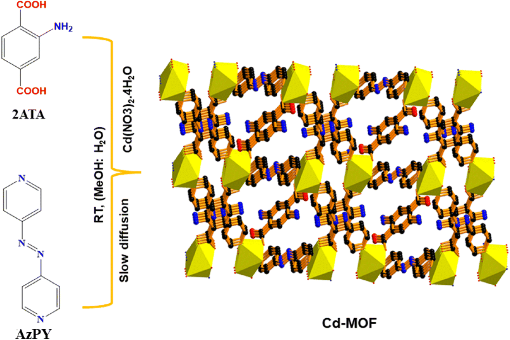 | ||
| Scheme 1 Schematic illustrations for the synthesis of the Cd-metal organic framework. | ||
Single crystal X-ray analysis was used to determine the crystal structure of Cd-MOF. It suggests that the Cd-MOF crystallizes in a triclinic system with the P![[1 with combining macron]](https://www.rsc.org/images/entities/char_0031_0304.gif) space group. The other crystal structure data and refinement parameters are summarised in Table S1.† The asymmetric unit consists of one Cd(II) metal ion, half of two azopyridine (AzPY) units, two-quarter units of 2-aminoterephthalic acid (2-ATA), and one water molecule Fig. S1a.† To determine the molecular unit of Cd-MOF, each Cd II unit is coordinated to three oxygen atoms of 2-ATA, two N-atom of AzPY and one oxygen atom of water molecule, as depicted in Fig. 1a, whereas in the case of the coordination mode of the 2ATA ligand, two amino groups present in the same benzene ring cannot coexist, so these free amine groups are in a disordered state.38 The binding mode of 2ATA and AzPY linkers with Cd metal is shown in Fig. S1b–d.† This coordinated environment of O4N2 leads to distorted octahedral geometry around the metal center due to unequal bond distances with three oxygen atoms and the presence of one N atom in the axial position and one N atom in the equatorial position, as shown in Fig. S1e.†
space group. The other crystal structure data and refinement parameters are summarised in Table S1.† The asymmetric unit consists of one Cd(II) metal ion, half of two azopyridine (AzPY) units, two-quarter units of 2-aminoterephthalic acid (2-ATA), and one water molecule Fig. S1a.† To determine the molecular unit of Cd-MOF, each Cd II unit is coordinated to three oxygen atoms of 2-ATA, two N-atom of AzPY and one oxygen atom of water molecule, as depicted in Fig. 1a, whereas in the case of the coordination mode of the 2ATA ligand, two amino groups present in the same benzene ring cannot coexist, so these free amine groups are in a disordered state.38 The binding mode of 2ATA and AzPY linkers with Cd metal is shown in Fig. S1b–d.† This coordinated environment of O4N2 leads to distorted octahedral geometry around the metal center due to unequal bond distances with three oxygen atoms and the presence of one N atom in the axial position and one N atom in the equatorial position, as shown in Fig. S1e.†
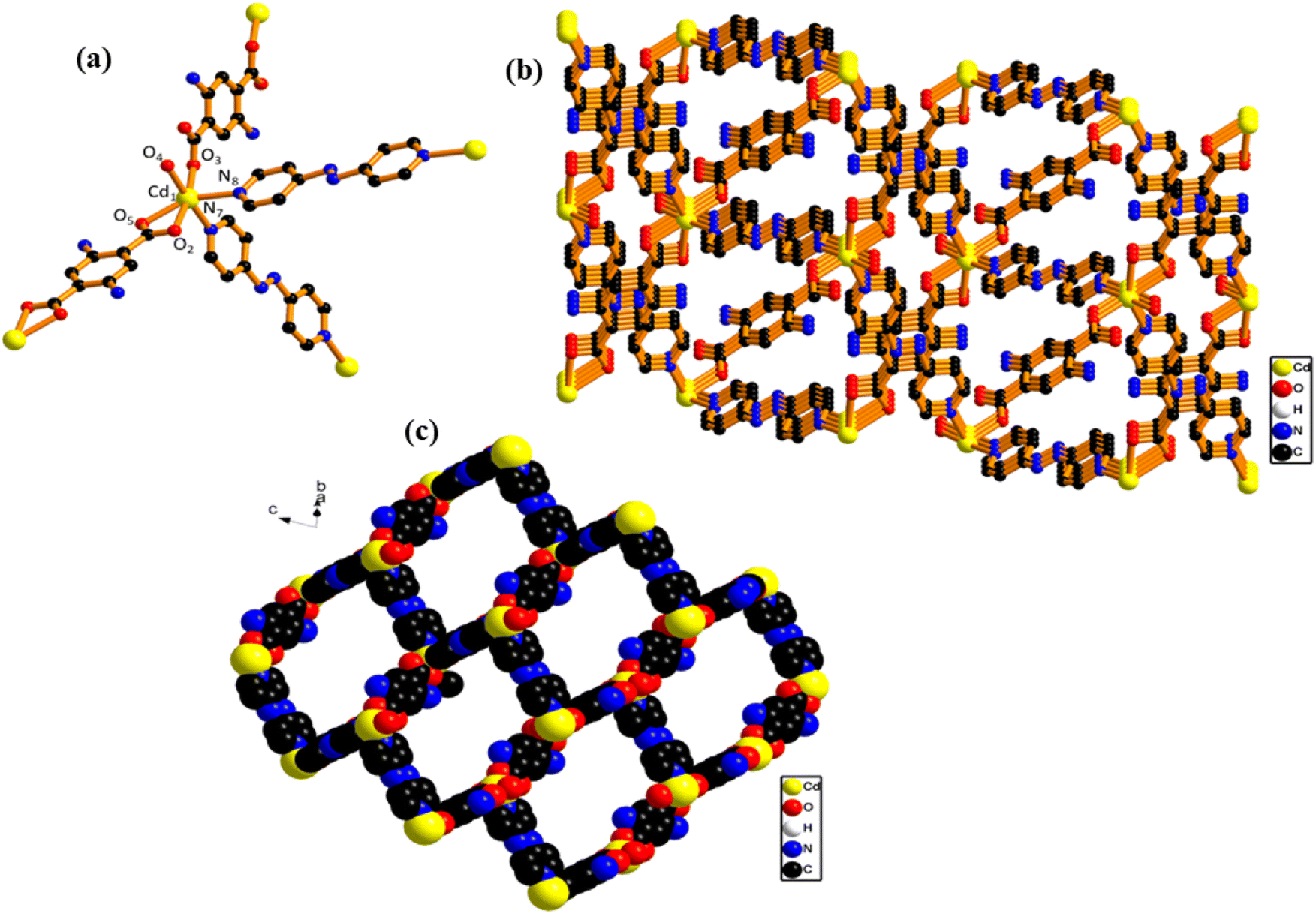 | ||
| Fig. 1 (a) Coordination mode of Cd(II) with ligands; (b) 2D framework of Cd-MOF along the a-axis; (c) 2D network along the a-axis; (d) space-filling model of rotation along the a-axis. | ||
The binding mode of 2ATA has been coordinated in a tetradentate fashion (μ4-κ1O3: κ2O2, O5: κ1O4), and AzPY is coordinated in a bidentate fashion (μ2-κ1N7: κ1N8) to Cd(II) ion which significantly helps in the formation of a 2D network of MOF. The measured bond distance of Cd–N is 2.331 to 2.350 Å, and the bond distance between Cd and O is 2.223 to 2.445 respectively. The measured bond angle for O–Cd–O and N–Cd–N is in the range of 84.25° to 98.74° and 85.65° respectively. The other significant bond length and bond angle are summarized in ESI in Table S2.† The ball and stick model of 2D Cd-MOF along the a-axis is shown in Fig. 1b. 2D networks along with polyhedra are shown in Fig. S2a† respectively, the 2D view of Cd-MOF along the a-axis provides stability to the overall framework network. The space-filling model of Cd-MOF, which is a slight rotation along the a-axis, shows the porous nature of Cd-MOF depicted in Fig. 1c and the metal-to-metal pore aperture is 20 Å to 27 Å as depicted in Fig. S2b,† thus exhibiting the functionalization of NH2 and H2O molecules coordinated in the crystal system. The NH2 group generally has a higher electron donating ability.
The phase purity and crystalline nature of Cd-MOF were determined by using PXRD analysis. The as-synthesized Cd-MOF is well matched with the simulated one obtained from SC-XRD analysis, as depicted in Fig. 2a. It signifies the materials having phase purity. Fig. S3a† shows the thermogravimetric analysis of Cd-MOF; initially, there is a weight loss of around 150 °C indicating the removal of solvent molecules (coordinated and cavity solvent) from the framework and the second loss occurs at around 340–400 °C, indicating the deformation of the framework network and the final residue is CdO. Furthermore, to determine the electrical properties of Cd-MOF by using dielectric measurement setup. A material's dielectric constant will often be greater if it has a high volumetric density and polar chemical groups. A highly porous structure of MOF tends to have a smaller value of dielectric constant due to the presence of air in the pores. MOFs having different structural topologies their volumetric densities will varies, this leads to the impact on dielectric constant. Since Cd-MOF has a polar C–NH2 bond and low porosity compared to the non-functionalized MOFs, it also has a dense structural framework and tends to have a better dielectric constant value with greater polarizability. For the present study, the dielectric properties of Cd-MOF have been studied at room temperature with different ranges of frequencies (MHz). The frequency-dependent variation of the dielectric constant for Cd-MOF is shown in Fig. 2b. The experimentally measured dielectric constant value for Cd-MOF is 2.1 at the frequency of 106 Hz. The surface area and permanent porosity of Cd-MOF were verified by using the N2 adsorption–desorption curve via Brunauer–Emmett–Teller (BET) analysis. The surface area of Cd-MOF is 178 m2 g−1 as shown in Fig. S3b.† To determine the charging interface of Cd-MOF we have performed zeta potential measurement by dispersing Cd-MOF in water and the obtained charge of the Cd-MOF is −16.2 mV; this is one of the factors influencing the charge accumulation, and the dispersant dielectric constant is 78.5 (Fig. S4†). The surface morphology of Cd-MOF was analyzed via scanning electron microscopy (SEM) analysis; it shows that the Cd-MOF has plate-like morphology as depicted in Fig. 2c–e and S5a† with different scales. The energy dispersive X-ray spectroscopy (EDS) mapping is shown in Fig. S5b–e.† The EDS mapping confirms the presence of Cd, N, C, and O. The structural morphological analysis confirmed the successful preparation of Cd-MOF.
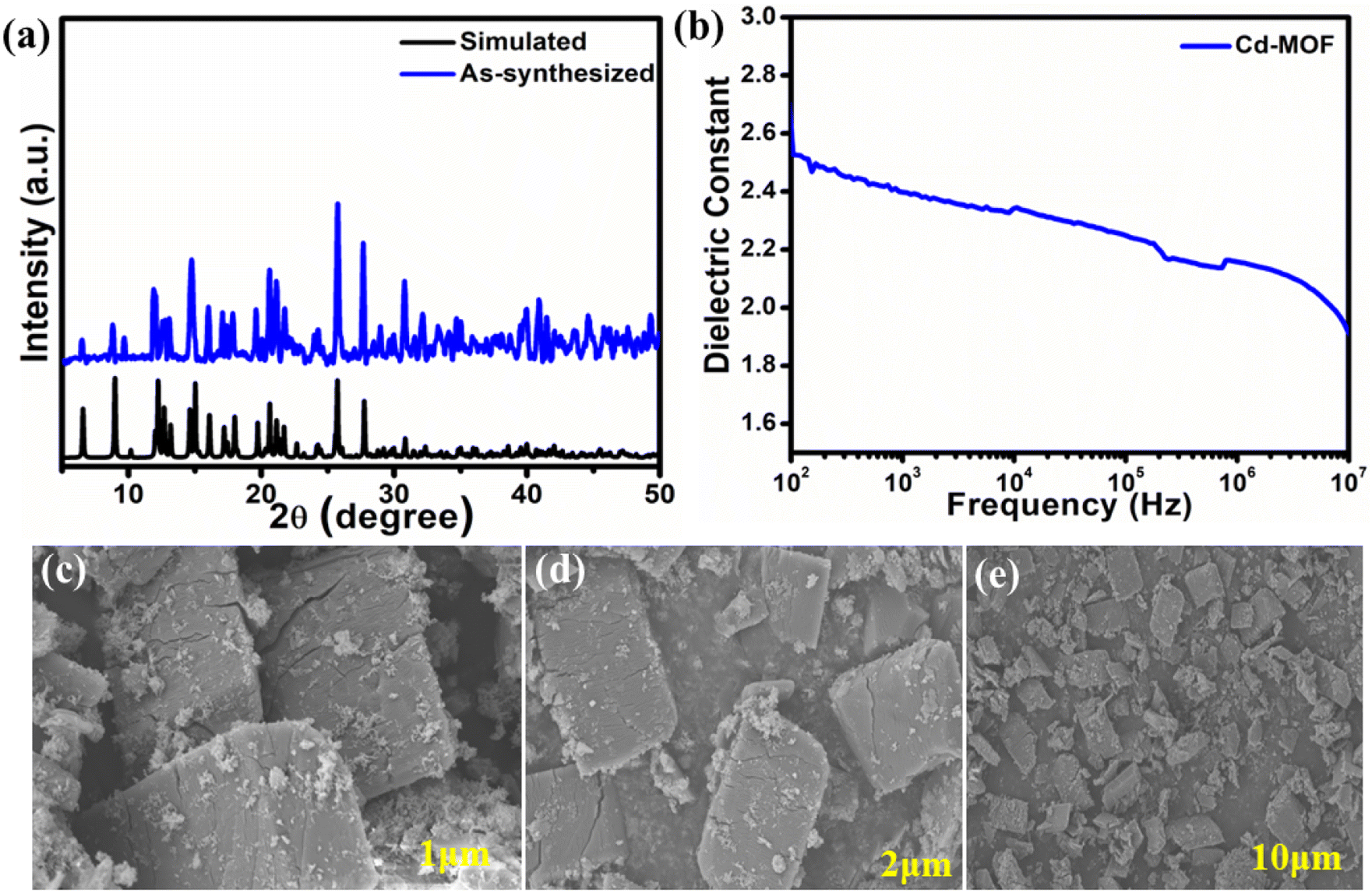 | ||
| Fig. 2 (a) PXRD pattern of Cd-MOF as-synthesized and simulated; (b) dielectric constant of Cd-MOF; (c–e) SEM images of Cd-MOF at different scales. | ||
Thus, after successful confirmation of Cd-MOF structure by analyzing various parameters such as morphology, zeta potential, surface area, dielectric constant measurement and stability of MOF, we further evaluated the output performance of TENG. The MOF/PDMS composite was used as the tribolayer for further study. MOFs usually interact very well with polymer matrices, which eventually minimize the creation of microvoids on the membrane surface. The highly conjugated and conductive azo-pyridine ligand of MOF, and the disordered NH2 functional group of the 2-ATA ligand interact with PDMS which provides stability for the MOF/PDMS composite film. Fig. S6† shows the XRD analysis of the pure PDMS and Cd-MOF/PDMS composite film. The hump between 10° and 20° is due to PDMS. The crystalline peaks of the Cd-MOF were observed along with the PDMS in the composite, which clearly show the particle loading in the film. The dielectric constants of the PDMS and MOF based composite were measured. A dielectric constant of 2.78 was obtained for the PDMS, and the MOF based composite has a dielectric constant of 3.1, as shown in Fig. S7.†
The improvement in the dielectric constant leads to an increase in the charge storing capability, which eventually reduces the surface charge decay. Fig. S8a† shows the SEM image of the pure PDMS and Cd-MOF/PDMS composite film. The pure PDMS film shows a flat nature. The Cd-MOF/PDMS based composite film shows the particle loaded in the film as shown in Fig. S8b.†Fig. 3a and b show the 3D roughness profile of the pure PDMS and MOF/PDMS composite film. The PDMS film shows an average roughness of 2.63 nm, and the composite film shows 9.78 nm. The increase in the roughness of the film increases the number of contact points for the triboelectrification. Cd-MOF based particles have negative surface potential, as shown by the zeta potential (Fig. S4†). The surface charge of the film was analyzed using the KPFM measurements. Fig. 3c and d show the surface charge mapping of PDMS and MOF based composite film. The PDMS film has an average surface charge of −53.679 mV, and the composite film has −71.379 mV. The change in the surface charges was due to the filling defects, dipoles, permittivity and charge transfer between the polymer and fillers. To understand the charge holding capacity of the composite film, surface charge decay was measured using KPFM. The surface charge of the samples was measured over a time interval of one hour. The measurement shows that the surface charges were reduced after one hour. The PDMS film shows a charge decay of 41.47%, and the MOF based composite shows 9.72%, which is less than that of PDMS. This is due to the charge holding capability of the filler in the composite film.
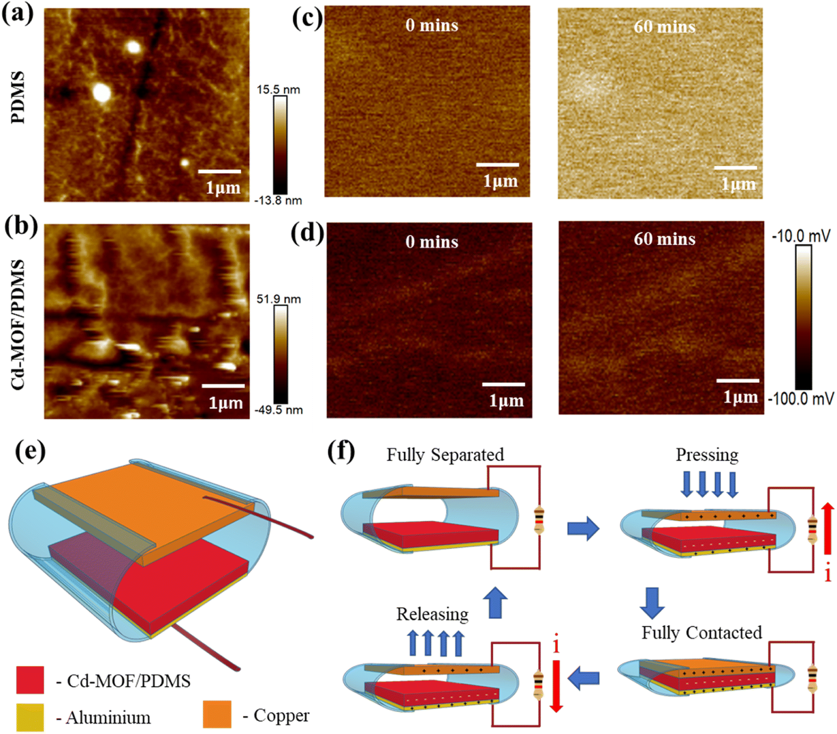 | ||
| Fig. 3 AFM topography for (a) bare PDMS, (b) Cd-MOF/PDMS films. KPFM potential plot at 0 min and 60 min for (c) bare PDMS, (d) Cd-MOF/PDMS films. (e) Schematic of the MOF-TENG device. (f) The working mechanism of the MOF-TENG device. | ||
The MOF-TENG device was fabricated with contact separation mode. Fig. 3e shows the schematic of the MOF-TENG device. Fig. 3f shows the working mechanism of the MOF-TENG device. The triboelectrification consists of three processes: contact electrification (generation of surface charge), charge holding (trapping sites) and electrostatic induction (induced charge at the electrode). Contact electrification depends on the electrophilic and nucleophilic sites of the different tribolayers. The charge trapping depends on polymer matrix polarization and interfaces of the polymer composite with the fillers. A metal electrode induces charges depending on the tribo charges due to the electrostatic induction. Under fully separated and contacted conditions, the charges of the electrode are under equilibrium, and the current flow does not occur. During the releasing and pressing states, the charges develop between the active layers, inducing an opposite charge to the electrode by electrostatic induction.36,39 It causes a potential difference and creates a current flow. Fig. 4a–f show the electrical characteristics of the MOF-TENG device. MOF-TENG with different wt% MOF loaded PDMS films were tested. The pure PDMS film delivers an output performance of 108 V and 0.409 μA. The output performance of the Cd-MOF/PDMS film increased till 2 wt% film. A maximum output voltage of 193.4 V and peak-to-peak current of 0.86 μA were achieved for the 2 wt% composite film as shown in Fig. 4a and b. The change in the output performance of the different composite films is due to the change in the surface charge, roughness and dielectric constant of the film. An acceleration dependent study was carried out in order to study the mechanical influence of triboelectrification. As shown in Fig. 4c, the output performance of the device improved till 2.5 m s−2 acceleration. Contact electrification depends on the charge transfer between the electrophilic and nucleophilic sites and this transfer is limited by the surface contact points and time. Increase in the acceleration at a certain point causes reduction in the charge transfer between the layers. The proposed TENG was studied under different relative humidity conditions, as shown in Fig. 4d. The output decreases with the increasing relative humidity conditions.
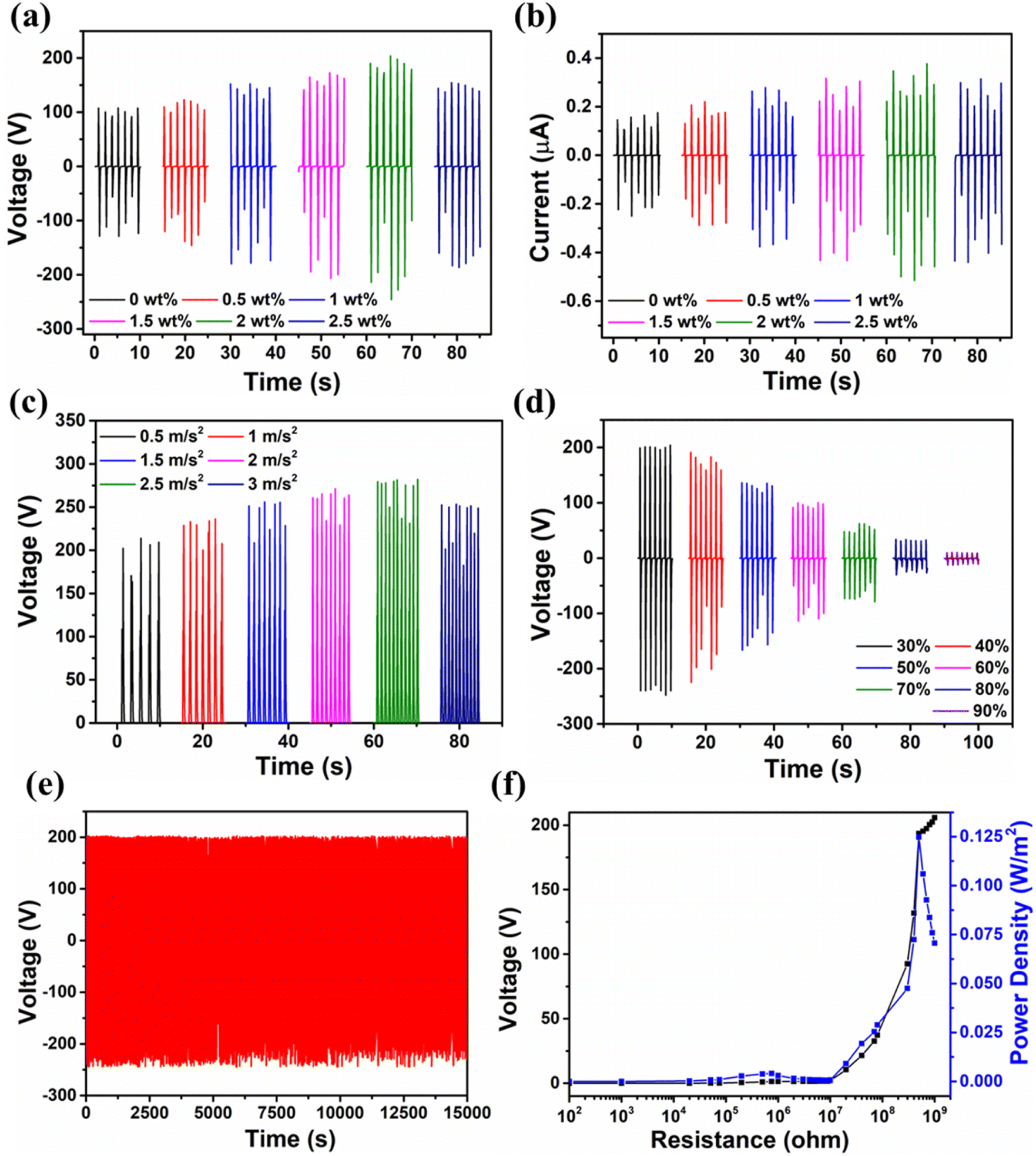 | ||
Fig. 4 The electrical output of the MOF-TENG device. (a) Output voltage and (b) current of the MOF-TENG device with different weight loadings under an applied mechanical force. (c) Output voltage under different applied accelerations from 0.5 m s−2 to 3 m s−2. (d) Output voltage under different humidity conditions from 30% to 90% RH. (e) Stability of MOF-TENG over 15![[thin space (1/6-em)]](https://www.rsc.org/images/entities/char_2009.gif) 000 s. (f) Load matching studies. 000 s. (f) Load matching studies. | ||
The humidity effect on the TENG can be reduced or eliminated using the package technology that was recently reported.40 Fig. S9† shows the temperature dependent study of the proposed TENG using a hair dryer. The temperature has been measured for the three hot air blowing states. The increase in temperature shows a slight change in the peak to peak voltage output. Z. L. Wang and co-workers studied the temperature effect of the triboelectric nanogenerator.41 They found that at less than 20 °C and more than 100 °C, the output change was vigorous. Between 20 °C and 60 °C, the output change was not drastic. These results are matched with those of the reported study. As depicted in Fig. 4e, the MOF-TENG device showed long stability for more than 15000 s (10500 cycles) without any noticeable decrease in the output. Fig. 4f shows the load matching studies. The MOF-TENG device had a maximum output power density of 0.124 W m−2 at a load resistance of 500 MΩ. The output charge profile for the MOF-TENG was observed to be 0.1 mC m−2 and is as shown in Fig. S10.† Table S3† reports the comparison table for different reported MOF and COF materials.
The commercial capacitor charging of MOF-TENG was carried out. The commercial capacitors of 0.47 μF, 1 μF, and 4.7 μF attain the maximum voltage of 14.52 V, 8.66 V, and 3.66 V respectively, within 300 s, as shown in Fig. 5a. Fig. 5b shows the continuous charging and discharging of the 0.47 μF capacitor. The charge and energy stored in the 4.7 μF capacitor are shown in Fig. 5c. The maximum charge and energy stored in the capacitor are 17 μC and 32.02 μJ respectively. The charge and energy stored in the capacitor at different intervals of time are shown in Fig. 5d. To show the device's capability, low power electronics was tested. The MOF-TENG device was able to power more than 60 green LEDs (Fig. 5e and ESI Video M1†), and it also managed to power a hygrometer for few seconds after charging a 60 μF capacitor (Fig. 5f and ESI Video M2†).
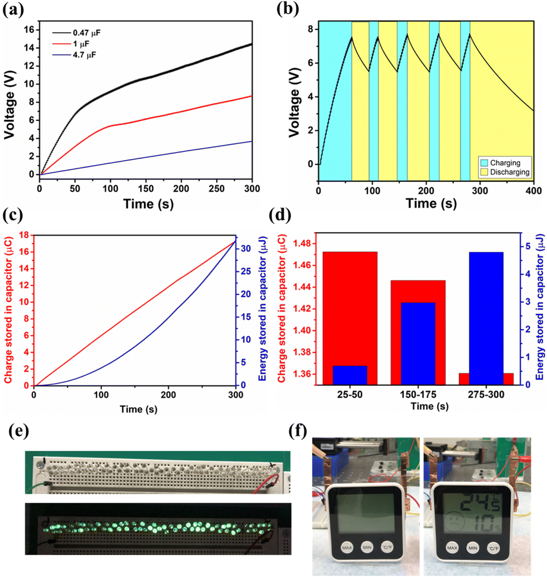 | ||
| Fig. 5 (a) Charging capacitors of 0.4 μF, 1 μF, and 4.7 μF using the MOF-TENG. (b) Continuous charging and discharging of the 0.47 μF capacitor. (c) Charge and energy stored in the 4.7 μF capacitor. (d) Charge and energy stored in the 4.7 μF capacitor at different time intervals. Powering of (e) 30 green LEDs and (f) a hygrometer using the MOF-TENG device. | ||
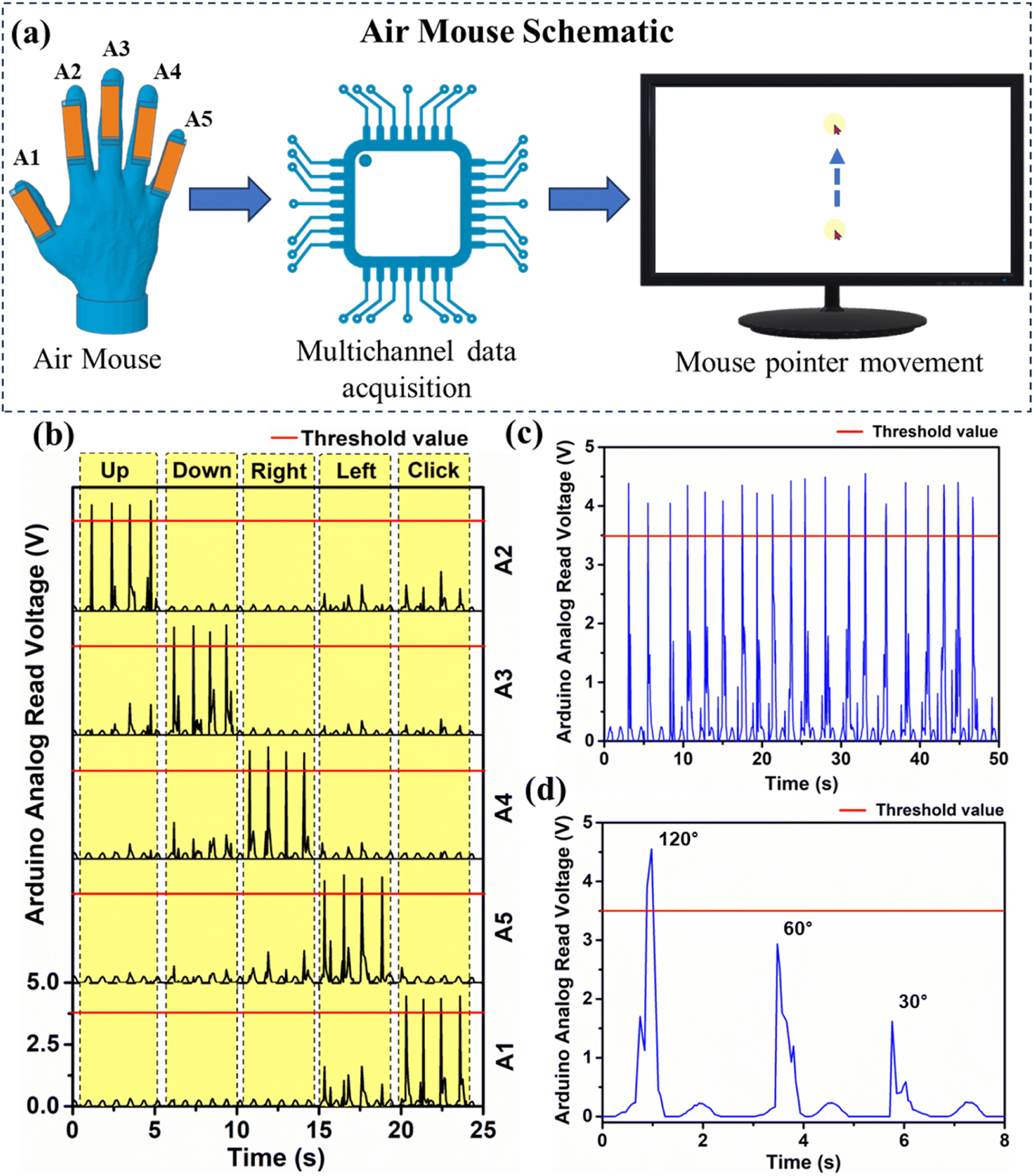
Using a touchpad, a mouse was controlled. Here a smart touchless air mouse was developed using the MOF-TENG device. The schematic of the air mouse system is shown in Fig. 6a. A device of size 5 × 1 cm2 was fabricated with the same active layers of the MOF-TENG. Five such devices (labelled A1–A5) were attached to the top of the fingers in a glove. When the finger is bent, the MOF-TENG device creates a signal (mechano-electric conversion). A multichannel data acquisition system (MDQ) (Arduino Micro) was used to collect the conditioned signal from the MOF-TENG device. The MDQ analyses the signal and compares it with a preset threshold value. If the signal value obtained is more than the threshold value, then the MDQ sends a signal to the computer to move the mouse pointer in a specific direction. The device labelled A1 is attached to the thumb and is assigned to do the click function, A2 to the index finger and to move the cursor up, A3 to the middle finger and to move the cursor down, A4 to the ring finger and to move the cursor right, and A5 to the little finger and to move the cursor left.
 | ||
| Fig. 6 (a) Schematic of the Air Mouse using MOF-TENG. Output from the Air Mouse (b) corresponding to individual finger movement, (c) showing stability for 50 seconds, (d) output at different bending angles. | ||
ESI Fig. S11a and b† show the digital image of the air mouse system. Fig. 6b shows the signal read by the MDQ. When the index finger is bent, the channel connected to A2 will get excited, and the MDQ will command the computer to move the mouse pointer up. Similarly, bending of the other fingers will perform the assigned mouse movements as demonstrated in ESI Videos M3 and M4†.
Single finger flexion leads to disturbance with the other fingers. This may cause electrification in the other device. Since the signal value is lower than the threshold signal, the respective action is ignored. The device stability is an essential factor while going for practical applications. Fig. 6c shows the output for the device crossing the threshold with the continuous bending of the fingers. Fig. 6d shows the output response for different bending angles of 120°, 60°, and 30° for the device labelled A2.
The device was used for biomechanical energy harvesting from hand tapping and foot tapping. Fig. 7a and b show the output characteristics of hand tapping and foot tapping respectively. The electrical output generated for hand tapping was observed to be around 150 V peak-to-peak and for the foot tapping it was around 70 V. Further capacitor charging was carried out using the device as shown in Fig. 7c. The 0.47 μF capacitor was charged up to 9.02 V and 2.31 V for hand and foot tapping respectively. Fig. 7d shows the schematic of the exercise monitoring using the prepared glove with the MOF-TENG device. The multiple devices were connected in series and parallel to determine the electrical characteristics. Fig. 7e shows the maximum voltage obtained with the series connection. Furthermore, the capacitor charging was tested with a 0.47 μF commercial capacitor for both series and parallel connections, Fig. 7f. Using this information, the count and calories burnt during the exercise can be calculated. The number of repeated cycles of exercise is equal to the number of full waves generated during the exercise. The calorie burnt can be calculated using the formula MET (for a therapeutic exercise ball, MET-2.8) × weight of the person × time duration (3.126 calories burned).
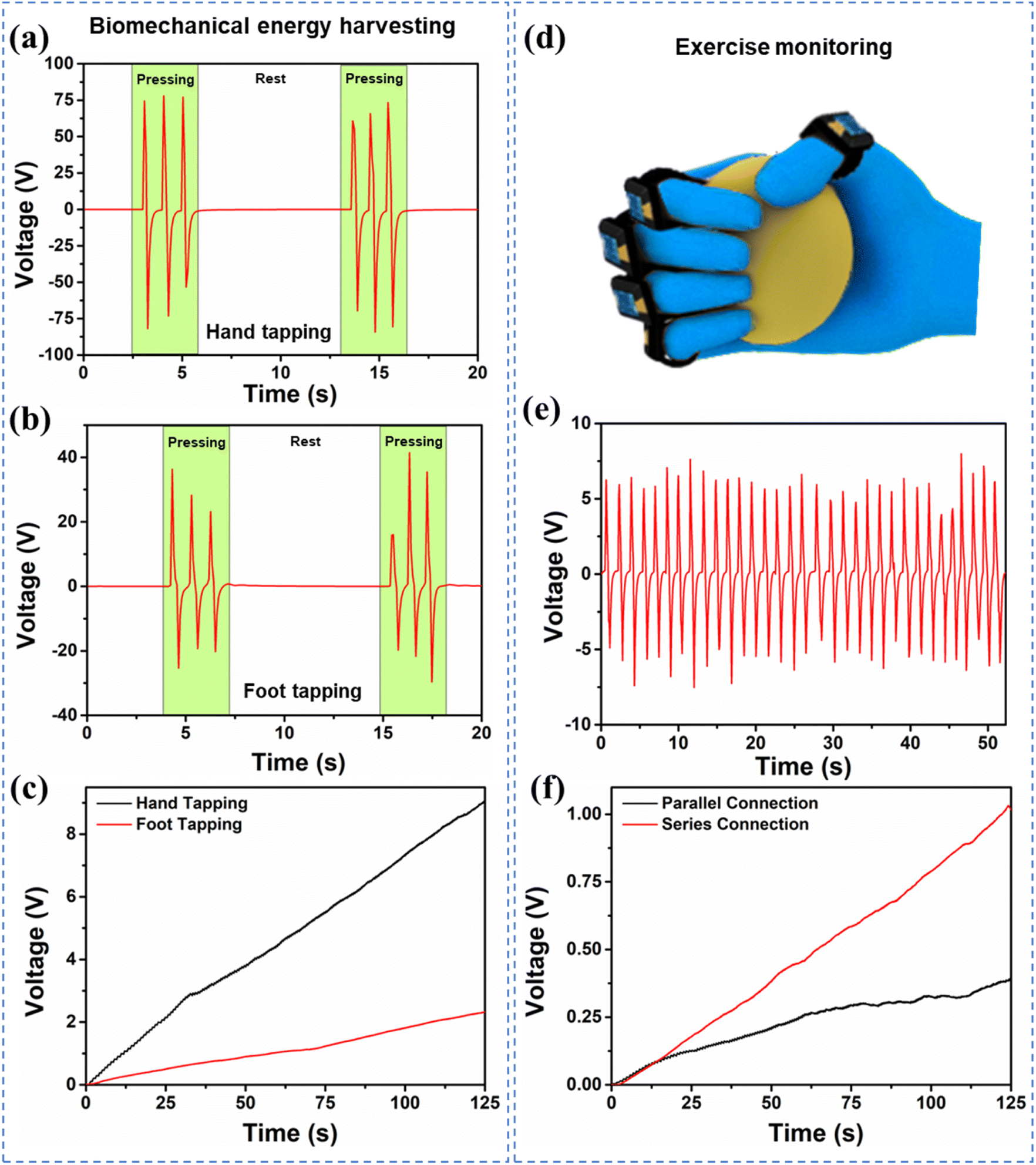 | ||
| Fig. 7 Output voltage for biomechanical energy harvesting for (a) hand pressing, (b) foot tapping. (c) Capacitor charging of the 0.47 μF capacitor by hand and foot tapping. (d) Schematic of energy harvesting from an exercise ball. (e) Output voltage, (f) capacitor charging of the 0.47 μF capacitor from the exercise ball. | ||
Experimental section
X-ray crystallography study and data refinement
The Cd-MOF single crystal structure was obtained by using a Rigaku Oxford Supernova CCD diffractometer. The single-crystal X-ray diffraction (SCXRD) analysis was performed at 293 K using monochromatic graphite Cu K (1.548), and the collection was detected using CrysAlisPro CCD software. Data reduction and cell refinement was carried out using CrysAlisPro RED software. Using the crystallographic software SHELXL-97, the structures were directly solved and improved using a full matrix least-squares method based on F2.42 All atoms were located using direct methods, while all non-H elements were obtained using anisotropic methods. The isotropic temperature factors that were used to refine all of the H atoms were typically 1.2Ueq of their parent atoms and were applied in geometrically controlled locations. The non-covalent electrostatic interaction, mean-plane determination, and molecular diagrams are produced by the DIAMOND program, version 3.1d.43 The Cd-MOF structure shows some disorder and unresolvable twinning problems due to which the NH2 group exists in two positions and also this leads to both the Alert B in the check CIF file.Synthesis of Cd-MOF
In a typical synthesis process, an aqueous solution (0.2 mmol 56 mg) of Cd (NO3)2·4H2O (2 mL) was prepared. Simultaneously, 2-aminoterephthalic acid (0.1 mmol 18.1 mg) in methanol (2 mL) were mixed with a methanolic solution (2 mL) of 4,4-azo pyridine (0.1 mmol, 18.4 mg) and stirred to become a clear solution. 2 mL of metal salt was placed in a crystallization tube and 2 mL of a 1:1 methanol/water buffer solution was placed above the metal salt solution and the third layer of mixed ligand solution was placed above the buffer solution. The tube was sealed with parafilm and placed without any disturbance at ambient temperature to allow the diffusion process. After one weak crystal growth occurs at the wall of the crystallization tube. Finally, the prepared crystals were separated and washed with water and methanol and characterized via SC-XRD analysis.
Preparation of the Cd-MOF/PDMS film
The composite film of Cd-MOF/PDMS was prepared by first making the PDMS solution by mixing a silicon elastomer and curing agent in a 10:1 ratio. The solution was mixed thoroughly and different wt% of Cd-MOF (0.5, 1, 1.5, 2, 2.5 wt%) was mixed into the PDMS solution and mixed again for 10 min under hand stirring. The solution was kept undisturbed to remove the air bubbles. The composite films were prepared via spin coating. The solution was poured onto a Petri dish covered with aluminium foil (which will act as the electrode) and spin-coated at 1000 rpm for 2 min. The films were cured at 70 °C for 2 h. The cured films were used for the fabrication of the TENG device.
Fabrication of the MOF-TENG device
The MOF-TENG device consists of Cd-MOF/PDMS film with an aluminium electrode and copper as the opposite layer/electrode. Both the layers were cut in the dimension of 2 × 3 cm2 and copper wires were connected to the electrodes using silver paste for collecting the generated output. Kapton tape was used to cover the silver paste connection, and a PET layer was kept for supporting the layers. Another PET layer was used for the side support for separating the layers after the mechanical force is removed. The schematic of the device structure is given in Fig. 3e. The device dimensions for the air mouse application were 5 × 1 cm2.Conclusions
In summary, of this work we incorporated a newly synthesized Cd-MOF as a filler into the PDMS polymer matrix for the fabrication of a highly durable TENG device. Due to improved dielectric properties, the charge trapping and charge generating properties of the film were improved. The electrical characterization of the different composite films was carried out and 2 wt% composite film showed a maximum output performance of 193.4 V and 0.86 μA and a maximum power density of 0.124 W m−2 at 500 MΩ load resistance. The MOF-TENG device was observed to have a long stability of more than 15000 s. The device was used for operating low-powered electronics such as LEDs and hygrometers. Furthermore, the MOF-TENG device was used for implementing a smart device called an air mouse by attaching the device to the fingers and controlling the mouse pointer by the movement of fingers. The MOF-TENG device was used for biomechanical energy harvesting and exercise monitoring. This work can pave the way for the use of MOF-based TENG devices and also for the development of various smart applications. Thus, by considering the strategy of this work, Cd-MOF as a filler remarkably improved the TENG performance with high durability.
Conflicts of interest
The authors declare no competing financial interest.Acknowledgements
S. M. M. thanks SERB-DST, New Delhi, India (Project CRG/2020/001769), BRNS, Mumbai, India (Project 58/14/17/2020-BRNS/37215), and IIT Indore for financial support. The research work was supported by the Basic Science Research Program through the National Research Foundation of Korea (NRF) grant funded by the Korean government (MSIT) (2021R1A4A2000934, 2023R1A2C3004336). Z. A. thanks CSIR for providing fellowship. N. H. thanks SERB for the fellowship. The authors acknowledge Sophisticated Instrumentation Centre, IIT Indore for all of the characterization facilities. We are thankful to Professor. Pankaj Sagdeo, Department of Physics, IIT Indore, for the dielectric measurement.References
- Z. Shao, J. Chen, K. Gao, Q. Xie, X. Xue, S. Zhou, C. Huang, L. Mi and H. Hou, Angew. Chem., Int. Ed., 2022, 61, e202208994 CrossRef CAS PubMed.
- Z. Shao, J. Chen, K. Gao, Q. Xie, X. Xue, X. Li, H. Hou and L. Mi, Chem. Eng. J., 2023, 455, 140865 CrossRef CAS.
- D. Choi, Y. Lee, Z.-H. Lin, S. Cho, M. Kim, C. K. Ao, S. Soh, C. Sohn, C. K. Jeong, J. Lee, M. Lee, S. Lee, J. Ryu, P. Parashar, Y. Cho, J. Ahn, I.-D. Kim, F. Jiang, P. S. Lee, G. Khandelwal, S.-J. Kim, H. S. Kim, H.-C. Song, M. Kim, J. Nah, W. Kim, H. G. Menge, Y. T. Park, W. Xu, J. Hao, H. Park, J.-H. Lee, D.-M. Lee, S.-W. Kim, J. Y. Park, H. Zhang, Y. Zi, R. Guo, J. Cheng, Z. Yang, Y. Xie, S. Lee, J. Chung, I.-K. Oh, J.-S. Kim, T. Cheng, Q. Gao, G. Cheng, G. Gu, M. Shim, J. Jung, C. Yun, C. Zhang, G. Liu, Y. Chen, S. Kim, X. Chen, J. Hu, X. Pu, Z. H. Guo, X. Wang, J. Chen, X. Xiao, X. Xie, M. Jarin, H. Zhang, Y.-C. Lai, T. He, H. Kim, I. Park, J. Ahn, N. D. Huynh, Y. Yang, Z. L. Wang, J. M. Baik and D. Choi, ACS Nano, 2023, 17, 11087–11219 CrossRef CAS PubMed.
- T. Trung Luu, N. Dinh Huynh, H. Kim, Z.-H. Lin and D. Choi, Nanoscale, 2023, 15, 14205–14214 RSC.
- K. Gao, J. Chen, M. Zhao, R. Hu, S. Chen, X. Xue, Z. Shao and H. Hou, Dalton Trans., 2023, 52, 444–451 RSC.
- F.-R. Fan, Z.-Q. Tian and Z. Lin Wang, Nano Energy, 2012, 1, 328–334 CrossRef CAS.
- D. W. Kim, J. H. Lee, J. K. Kim and U. Jeong, NPG Asia Mater., 2020, 12, 1–17 CrossRef.
- G. Khandelwal, N. P. M. J. Raj and S.-J. Kim, J. Mater. Chem. A, 2020, 8, 17817–17825 RSC.
- C. Rodrigues, D. Nunes, D. Clemente, N. Mathias, J. M. Correia, P. Rosa-Santos, F. Taveira-Pinto, T. Morais, A. Pereira and J. Ventura, Energy Environ. Sci., 2020, 13, 2657–2683 RSC.
- Y. Zeng, H. Xiang, N. Zheng, X. Cao, N. Wang and Z. L. Wang, Nano Energy, 2022, 91, 106601 CrossRef CAS.
- C. Xu, Y. Zi, A. C. Wang, H. Zou, Y. Dai, X. He, P. Wang, Y.-C. Wang, P. Feng, D. Li and Z. L. Wang, Adv. Mater., 2018, 30, 1706790 CrossRef PubMed.
- H. Zou, Y. Zhang, L. Guo, P. Wang, X. He, G. Dai, H. Zheng, C. Chen, A. C. Wang, C. Xu and Z. L. Wang, Nat. Commun., 2019, 10, 1427 CrossRef PubMed.
- C. Garcia, I. Trendafilova, R. Guzman de Villoria and J. Sanchez del Rio, Nano Energy, 2018, 50, 401–409 CrossRef CAS.
- Q. Zhou, J. Pan, S. Deng, F. Xia and T. Kim, Adv. Mater., 2021, 33, 2008276 CrossRef CAS PubMed.
- D. Bhatia, S. H. Jo, Y. Ryu, Y. Kim, D. H. Kim and H.-S. Park, Nano Energy, 2021, 80, 105508 CrossRef CAS.
- A. P. S. Prasanna, G. Khandelwal and S.-J. Kim, in Handbook of Triboelectric Nanogenerators, ed. Z. L. Wang, Y. Yang, J. Zhai and J. Wang, Springer International Publishing, Cham, 2023, pp. 1–20 Search PubMed.
- J.-K. Kim, G. Hyeon Han, S.-W. Kim, H. Jun Kim, R. Purbia, D.-M. Lee, J. Kyu Kim, H. Jae Hwang, H.-C. Song, D. Choi, S.-W. Kim, Z. Lin Wang and J. Min Baik, Energy Environ. Sci., 2023, 16, 598–609 RSC.
- Y. Liu, W. Sun, M. Feng, T. Li and D. Wang, Adv. Mater. Interfaces, 2022, 9, 2201287 CrossRef CAS.
- G. Wang, Y. Xi, H. Xuan, R. Liu, X. Chen and L. Cheng, Nano Energy, 2015, 18, 28–36 CrossRef CAS.
- S. Kim, M. K. Gupta, K. Y. Lee, A. Sohn, T. Y. Kim, K.-S. Shin, D. Kim, S. K. Kim, K. H. Lee, H.-J. Shin, D.-W. Kim and S.-W. Kim, Adv. Mater., 2014, 26, 3918–3925 CrossRef CAS PubMed.
- V. Mohan, V. K. Mariappan, P. Pazhamalai, K. Krishnamoorthy and S.-J. Kim, Carbon, 2023, 205, 328–335 CrossRef CAS.
- A. P. Sathya Prasanna, V. Vivekananthan, G. Khandelwal, N. R. Alluri, N. P. Maria Joseph Raj, M. Anithkumar and S.-J. Kim, ACS Sustainable Chem. Eng., 2022, 10, 6549–6558 CrossRef CAS.
- A. Sultana, P. Sadhukhan, Md. M. Alam, S. Das, T. R. Middya and D. Mandal, ACS Appl. Mater. Interfaces, 2018, 10, 4121–4130 CrossRef CAS PubMed.
- G. Pace, A. E. del Rio Castillo, A. Lamperti, S. Lauciello and F. Bonaccorso, Adv. Mater., 2023, 35, 2211037 CrossRef CAS PubMed.
- Z. Shao, J. Chen, Q. Xie and L. Mi, Coord. Chem. Rev., 2023, 486, 215118 CrossRef CAS.
- V. Kumar, P. Kumar, R. Deka, Z. Abbas and S. M. Mobin, Chem. Rec., 2022, 22, e202200067 CrossRef CAS PubMed.
- Z. Abbas, N. Hussain, I. Ahmed and S. M. Mobin, Inorg. Chem., 2023, 62, 8835–8845 CrossRef CAS PubMed.
- Y. Guo, Y. Cao, Z. Chen, R. Li, W. Gong, W. Yang, Q. Zhang and H. Wang, Nano Energy, 2020, 70, 104517 CrossRef CAS.
- Y.-M. Wang, X. Zhang, C. Liu, L. Wu, J. Zhang, T. Lei, Y. Wang, X.-B. Yin and R. Yang, Nano Energy, 2023, 107, 108149 CrossRef CAS.
- R. Wen, J. Guo, A. Yu, J. Zhai and Z. lin Wang, Adv. Funct. Mater., 2019, 29, 1807655 CrossRef.
- Z. Chen, Y. Cao, W. Yang, L. An, H. Fan and Y. Guo, J. Mater. Chem. A, 2022, 10, 799–807 RSC.
- M. Anithkumar, A. P. S. Prasanna, N. R. Alluri and S.-J. Kim, Adv. Funct. Mater., 2023, 33, 2213907 CrossRef CAS.
- S. Shen, X. Xiao, J. Yin, X. Xiao and J. Chen, Small Methods, 2022, 6, 2200830 CrossRef PubMed.
- L. Zu, J. Wen, S. Wang, M. Zhang, W. Sun, B. Chen and Z. L. Wang, Sci. Adv., 2023, 9, eadg5152 CrossRef CAS PubMed.
- Y. Zou, Y. Gai, P. Tan, D. Jiang, X. Qu, J. Xue, H. Ouyang, B. Shi, L. Li, D. Luo, Y. Deng, Z. Li and Z. L. Wang, Fundam. Res., 2022, 2, 619–628 CrossRef.
- K. Shi, H. Zou, B. Sun, P. Jiang, J. He and X. Huang, Adv. Funct. Mater., 2020, 30, 1904536 CrossRef CAS.
- Y. Gai, E. Wang, M. Liu, L. Xie, Y. Bai, Y. Yang, J. Xue, X. Qu, Y. Xi, L. Li, D. Luo and Z. Li, Small Methods, 2022, 6, 2200653 CrossRef CAS PubMed.
- Z. Gao, X. Zhang, P. Xu and J. Sun, Inorg. Chem. Front., 2020, 7, 1995–2005 RSC.
- C. Xu, Y. Zi, A. C. Wang, H. Zou, Y. Dai, X. He, P. Wang, Y.-C. Wang, P. Feng, D. Li and Z. L. Wang, Adv. Mater., 2018, 30, 1706790 CrossRef PubMed.
- A. Chandrasekhar, V. Vivekananthan and S.-J. Kim, Nano Energy, 2020, 69, 104439 CrossRef CAS.
- C. X. Lu, C. B. Han, G. Q. Gu, J. Chen, Z. W. Yang, T. Jiang, C. He and Z. L. Wang, Adv. Eng. Mater., 2017, 19, 1700275 CrossRef.
- G. M. Sheldrick, Acta Crystallogr., Sect. A: Found. Crystallogr., 2008, 64, 112–122 CrossRef CAS PubMed.
- G. Bergerhoff, M. Berndt and K. Brandenburg, J. Res. Natl. Inst. Stand. Technol., 1996, 101, 221 CrossRef CAS PubMed.
Footnotes |
| † Electronic supplementary information (ESI) available: SC-XRD data, TGA, BET, zeta potential, SEM EDS, PXRD, TENG data and photograph of the device attached to fingers and table of crystal parameters. CCDC 2287569. For ESI and crystallographic data in CIF or other electronic format see DOI: https://doi.org/10.1039/d3ta05178a |
| ‡ These authors contributed equally to this work. |
| This journal is © The Royal Society of Chemistry 2023 |