
 Open Access Article
 This Open Access Article is licensed under a Creative Commons Attribution-Non Commercial 3.0 Unported Licence
Cu2ZnSnS4 monograin layer solar cells for flexible photovoltaic applications
Marit
Kauk-Kuusik
 *a,
Kristi
Timmo
a,
Maris
Pilvet
a,
Katri
Muska
a,
Mati
Danilson
a,
Jüri
Krustok
a,
Raavo
Josepson
b,
Valdek
Mikli
a and
Maarja
Grossberg-Kuusk
a
*a,
Kristi
Timmo
a,
Maris
Pilvet
a,
Katri
Muska
a,
Mati
Danilson
a,
Jüri
Krustok
a,
Raavo
Josepson
b,
Valdek
Mikli
a and
Maarja
Grossberg-Kuusk
a
aLaboratory of Photovoltaic Materials, Tallinn University of Technology, Ehitajate tee 5, Tallinn, Estonia. E-mail: marit.kauk-kuusik@taltech.ee
bDivision of Physics, Tallinn University of Technology, Ehitajate tee 5, Tallinn, Estonia
First published on 23rd October 2023
Abstract
Monograin powder technology is one possible path to developing sustainable, lightweight, flexible, and semi-transparent solar cells, which might be ideal for integration with various building and product elements. In recent years, the main research focus of monograin technology has centered around understanding the synthesis and optoelectronic properties of kesterite-type absorber materials. Among these, Cu2ZnSnS4 (CZTS) stands out as a promising solar cell absorber due to its favorable optical and electrical characteristics. CZTS is particularly appealing as its constituent elements are abundant and non-toxic, and it currently holds the record for highest power conversion efficiency (PCE) among emerging inorganic thin-film PV candidates. Despite its advantages, kesterite solar cells' PCE still falls significantly behind the theoretical maximum efficiency due to the large VOC deficit. This review explores various strategies aimed at improving VOC losses to enhance the overall performance of CZTS monograin layer solar cells. It was found that low-temperature post-annealing of CZTS powders reduced Cu–Zn disordering, increasing Eg by ∼100 meV and VOC values; however, achieving the optimal balance between ordered and disordered regions in kesterite materials is crucial for enhancing photovoltaic device performance due to the coexistence of ordered and disordered phases. CZTS alloying with Ag and Cd suppressed non-radiative recombination and increased short-circuit current density. Optimizing Ag content at 1% reduced CuZn antisite defects, but higher Ag levels compensated for acceptor defects, leading to reduced carrier density and decreased solar cell performance. Co-doping with Li and K resulted in an increased bandgap (1.57 eV) and improved VOC, but further optimization is required due to a relatively large difference between measured and theoretical VOC. Heterojunction modifications led to the most effective PCE improvement in CZTS-based solar cells, achieving an overall efficiency of 12.06%.
1. Introduction
Over the past few decades, the photovoltaic (PV) market has been largely dominated by silicon-based solar cells. However, there has been a noticeable shift towards PV technology based on flexible solar cells in recent times. This transition has been primarily driven by the growing demand for devices that offer high flexibility, lightweight characteristics, conformability, and bendability.Numerous approaches and materials have been investigated, such as flexible ultra-thin crystalline silicon (Si) solar cells,1 flexible chalcopyrite CuInGa(S,Se)2 (CIGSSe) thin-film solar cells,2 organic solar cells,3 perovskite solar cells,4 dye-sensitized solar cells (DSSCs), and other thin-film technologies. Each technology has its own advantages and challenges, and ongoing research aims to overcome limitations and improve efficiency, stability, and manufacturing processes. Flexible ultra-thin crystalline Si solar cells offer the advantage of using a well-established material with high efficiency. However, their fragility remains a concern, and limits their widespread adoption. Thin-film Si tandem solar cells and CIGSSe thin-film solar cells have shown promise in terms of flexibility and efficiency. However, their commercialization has been hindered by relatively high manufacturing costs, which have stalled their progress in recent years. Organic solar cells have the advantage of being lightweight, flexible, and potentially low-cost due to their compatibility with roll-to-roll manufacturing processes. However, their module efficiency and long-term stability have been areas of concern, and have limited their commercialization. Given these limitations and challenges, the search for alternative flexible solar cell technologies remains an active and important area of research in the field of photovoltaics.
The ultimate goal of this research is to achieve a breakthrough in kesterite flexible photovoltaic technology, enabling the mass production of sustainable high-performance solar cells that can be seamlessly integrated into various applications, ranging from portable electronics to wearable devices, building-integrated photovoltaics (BIPV), and beyond. By developing flexible photovoltaic technologies, it becomes possible to harness solar energy in environments and industries where traditional rigid solar panels are not viable or practical.
2. Monograin layer technology
Monograin layer technology (MGL) provides one way to prepare lightweight, semi-transparent, and flexible photovoltaics in the future. In Fig. 1 is shown the lab-scale flexible monograin layer device with a total size of 2.5 cm × 2.5 cm containing ∼100 solar cells (0.018 cm2).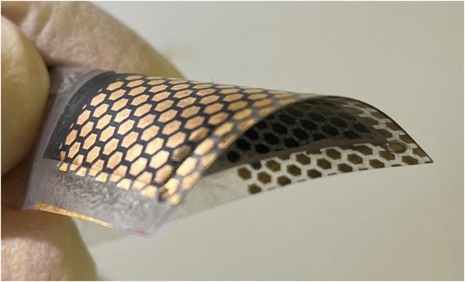 | ||
| Fig. 1 Photo of a flexible CZTS monograin layer device with size of 2.5 cm × 2.5 cm. | ||
MGL solar cell technology introduces significant innovations that contribute to its potential for high power conversion efficiencies (PCE) and cost-effectiveness. The MGL solar cell incorporates a light-absorbing layer composed of monograin powders. These powders are synthesized using the molten salt method,5–9 allowing for the growth of micro-crystalline semiconductor materials with precise control over their chemical composition and doping concentration. The process scheme of the monograin powder synthesis is presented in Fig. 2a. This precise control over the material properties results in high optical, electrical, and structural quality within the light-absorbing layer. The use of monograin powders enables the MGL solar cell to achieve theoretically higher PCE levels due to their single-crystal structure, which means there are fewer grain boundaries compared to polycrystalline materials, resulting in better light absorption, higher charge carrier mobility, and reduced recombination losses. The MGL technology involves a production process based on the roll-to-roll technique. This continuous and automated production method enables efficient and cost-effective fabrication of solar cell modules. The roll-to-roll process streamlines production, reduces material waste, and facilitates mass production, making the MGL solar cell technology economically viable for large-scale deployment.10 By combining these innovations, the MGL solar cell technology demonstrates the potential to significantly improve the efficiency of solar energy conversion while ensuring cost-effectiveness and scalability. The precise control over material properties achieved through monograin powders and the efficient roll-to-roll manufacturing process makes the MGL solar cell an attractive solution to advance the field of photovoltaics and promote widespread adoption of solar energy as a sustainable and renewable power source.
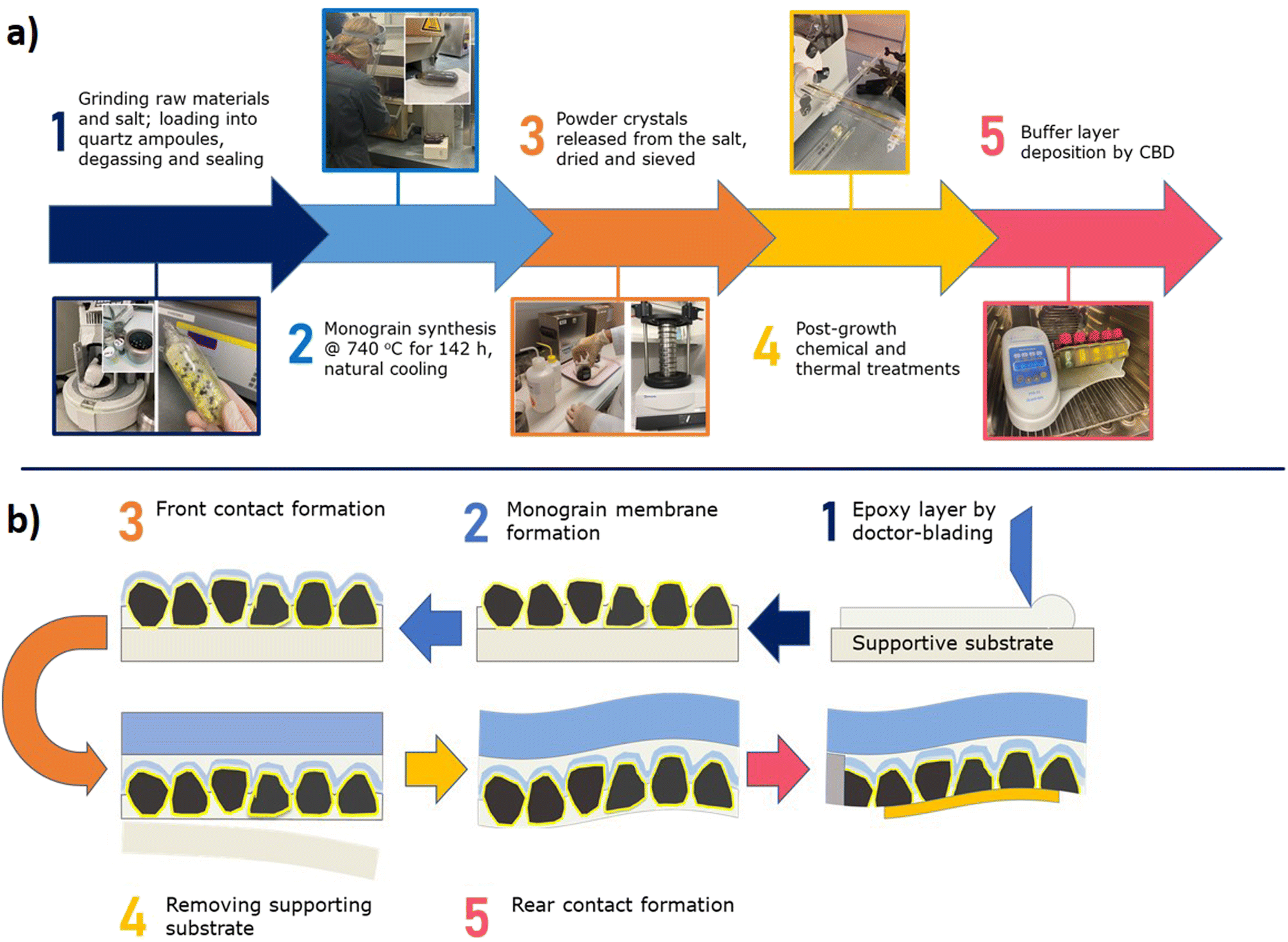 | ||
| Fig. 2 Scheme of (a) monograin powder preparation and (b) monograin layer fabrication. | ||
The monograin membranes are constructed using a specific fabrication technique that involves the incorporation of monograins within a thin layer of transparent, low shrinkage polymer during the curing process. The monograins together with the buffer layer are manufactured separately before entering the module production process (the formed heterojunction provides full photovoltaic functionality already at the monograin level) which is superior to the other thin film PV technologies.
The subsequent steps in the fabrication process include the deposition of additional layers such as transparent conductive electrodes and rear contacts, which are necessary for the complete construction of monograin layer solar cells. The schematic lab scale fabrication process of the complete monograin layer solar cell is presented in Fig. 2b.
An additional advantage of this technology is only minor waste of materials due to recyclability of unused fractions of monograin powder in the new synthesis process. The MGL technology offers a unique opportunity to turn an inherent technology disadvantage of the nonactive area (polymer) into a benefit and use it to transmit light. The transmission is almost uniform over the visible range and can be tuned by the crystal density. At the moment, the limiting factor is the lack of a suitable transparent back contact material. In thin film technologies, several binary oxides such as SnO2, In2O3, or ZnO have been investigated.11 However, a major challenge with these oxides is that they typically require relatively high deposition temperatures to achieve adequate conductivity. This high-temperature deposition process may not be suitable for monograin membranes due to them being sensitive to high temperatures. In contrast to substrate-configuration thin-film technologies, where the fabrication of the structure begins with back-contact deposition, in monograin layer solar cell technology, making the back-contact is the last step in the technological sequence. As shown in Fig. 2b, for back contacting, the supporting foil is removed from the back side, and the bottom side of the MGL is abraded with ultrafine sandpaper to remove polymer from powder crystals. With this process, a p+ layer on the back side of the crystals is created.12 This type of back contact helps hole tunnelling from the absorber bulk into the contact (currently Au or graphite is used). As there has been limited research on transparent back contacts, especially for kesterite and chalcopyrite technologies, further research is essential specifically for semi-transparent solar cells.
2.1. Challenges in CZTS monograin layer solar cells
In recent years, the main research focus of the monograin technology has been on the understanding of the synthesis and optoelectronic properties of kesterite type absorber materials. Kesterite, especially Cu2ZnSnS4 (CZTS), is a promising solar cell absorber due to its attractive optical and electrical properties – high absorption coefficient (∼10−4 cm−1), optimum band gap (1.5–1.6 eV) for photovoltaics, p-type conductivity, and tuneable band gap by alloying.13 Its constituent elements are earth-abundant and non-toxic, and it holds the highest (PCE) record (14.9%)14 among all emerging inorganic thin-film PV candidates. However, the PCE of kesterite solar cells is still much lower compared to the theoretical maximum efficiency (∼32%).15The performance of kesterite solar cells is limited by the large open circuit voltage (VOC) deficit (VSQOC − VOC). VSQOC is the maximum achievable VOC based on the Shockley–Queisser limit.16,17 Several factors can contribute to this loss of VOC, including: (1) the challenges in achieving a uniform absorber composition. Variations in composition can lead to fluctuations in the bandgap, resulting in reduced device performance. Additionally, the presence of secondary phases within the absorber can negatively impact the charge transport and recombination properties; (2) Cu–Zn antisite defects: Cu and Zn have similar ionic sizes, which can lead to the formation of Cu–Zn antisite defects. These defects introduce electrostatic potential fluctuations and band tailing within the kesterite material, affecting the overall device performance and reducing the VOC; (3) complex defect properties introduced by multivalent Sn: the presence of Sn as a multivalent element in the kesterite structure introduces complex defect properties. These defects can contribute to high recombination rates in both the bulk of the absorber material and at the interfaces, leading to a decrease in VOC.
Addressing these factors is crucial to improving the performance of kesterite solar cells. Researchers and engineers have been focusing on developing strategies to achieve a more uniform absorber composition, mitigate Cu–Zn antisite defects, and optimize the defect properties associated with multivalent Sn. By addressing these challenges, it is possible to enhance the efficiency and VOC of kesterite solar cells.
In the context of record efficiency devices, the kesterite-based solar cell with a PCE of 13.8% exhibits a VOC deficit value of approximately 304 mV.18 On the other hand, the CIGSSe solar cell, which achieves a higher PCE of 23.4%,19 has a VOC deficit value of approximately 164 mV, and therefore significant research is still needed in this field. In Fig. 3 is presented the evolution of efficiencies of the kesterite monograin layer solar cells. All PCE values correspond to the active area of the solar cell. PCE is calculated by using an image analysis tool for the active surface area (∼75% of total contact area).20,21 The first paper on kesterite monograin layer solar cells with PCE = 2.16% was published in 2008.22 Until 2015, there was significant progress in the MGL solar cell development, leading to a remarkable increase in efficiency up to 9.4%.23 Throughout this period, extensive research was dedicated to the refinement of optimal composition,7,24,25 post-treatment techniques,26,27 and surface passivation methods of kesterite absorber prior to the deposition of the CdS buffer layer.23 Despite continuous research and development efforts, the progress made in the following years to enhance the overall efficiency of kesterite-based monograin solar cells did not meet the desired expectations. Various strategies were explored, including doping and alloying with silver (Ag),28 cadmium (Cd)29–31 and lithium (Li),32 and soft-annealing of cadmium sulfide (CdS),12 among others. These approaches aimed to optimize the performance of kesterite-based solar cells. However, despite these attempts, the desired improvements in efficiency were not fully realized, highlighting the challenges and complexities associated with advancing kesterite solar cell technology. In this paper, we gather most of the findings related to pure Cu2ZnSnS4 monograin powders and solar cells.
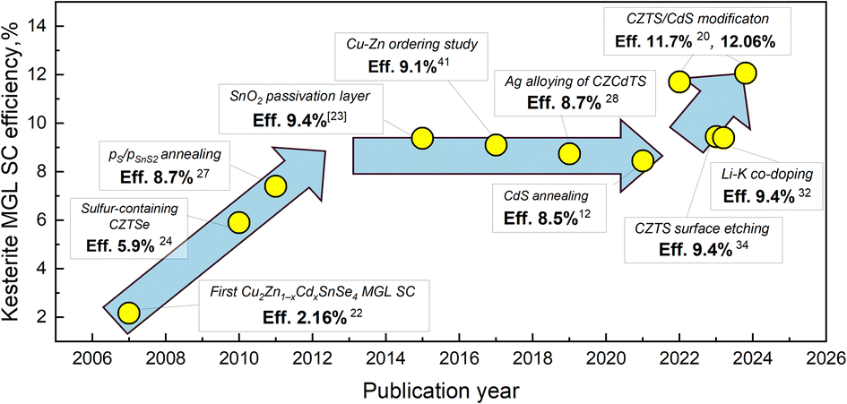 | ||
| Fig. 3 Evolution of kesterite monograin layer solar cell efficiency. | ||
In the well-developed synthesis process, high-purity Cu2ZnSnS4 monograin powder is produced through the reaction of binary compounds, namely CuS, ZnS, and SnS. The synthesis takes place in the liquid phase of a potassium iodide (KI) flux material within a sealed quartz ampoule at a temperature of 740 °C. The compositional ratios of Cu/(Zn + Sn) = 0.91 and Zn/Sn = 1.08 are used to achieve high-efficiency CZTS monograin layer solar cells. Our previous studies have demonstrated that this composition minimizes the formation of secondary phases.7 Single-phase CZTS powders can be successfully grown in a molten KI medium with initial metal ratios ranging from Cu/(Zn + Sn) ∼0.91–0.95 and Zn/Sn = 1.0–1.03. Larger deviations from stoichiometry resulted in different secondary phases such as Sn2S3, SnS2, Cu2−xS, and ZnS in addition to the CZTS powder crystals.
2.2. Post-growth chemical and thermal treatments
After the synthesis process, the CZTS powders undergo a chemical post-treatment process that involves complex etching with bromine (Br) in methanol (MeOH), followed by treatment with a potassium cyanide (KCN) aqueous solution at room temperature.33,34 This post-treatment is carried out to modify the surface of the CZTS powders, enhancing their properties for use in solar cell applications. In the study by Timmo et al.,34 the concentration of Br in MeOH solutions was varied from 0.05 v/v% to 10 v/v%. A concentration of 1 v/v% Br2–MeOH provided clean and flat surfaces without degrading the crystal shape. However, increasing the concentration above 1 v/v% resulted in an aggressive etching effect, leading to decreased crystal size and rough, porous surfaces. Therefore, controlling the concentration of the Br2–MeOH solution is crucial to achieve optimal etching results without compromising the crystal structure and surface morphology. After the etching process, the chemically treated CZTS powders undergo post-annealing to further enhance their properties. Post-annealing is carried out in a sealed quartz ampoule using a dual-temperature zone furnace. The annealing temperature is varied in the range of 550 to 850 °C, and the duration of the annealing process is 60 minutes.34 In addition to temperature variations, the sulphur pressure (PS) is also controlled during the post-annealing process. The PS is adjusted by changing the temperature on the sulphur side of the ampoule in the 330 to 550 °C range. This manipulation allows for a variation in PS from 100 to 2050 Torr. During the post-annealing process of the chemically treated CZTS powders, an important observation is that the compositional ratio of Cu/(Zn + Sn) in the bulk of the crystals increased (Fig. 4a), while the ratio of Zn/Sn decreased (Fig. 4b). This trend is consistent across all the different annealing temperatures and vapor pressures employed. The increase in the Cu/(Zn + Sn) ratio suggests that the post-annealing process promotes the diffusion or redistribution of copper within the CZTS crystals, leading to a higher Cu content in the bulk. In contrast, the decrease in the Zn/Sn ratio implies the migration of zinc to the CZTS crystal surface during the post-annealing process. These compositional changes observed in most of the post-annealed CZTS crystals indicate the influence of the annealing conditions on the elemental distribution and composition of the material. The precise control of these ratios through post-annealing is important to tailor the properties of the CZTS crystals, such as bandgap, defect concentration, and carrier transport, to optimize their performance in solar cell applications. The integration of etched and annealed powders in the MGL solar cells has yielded remarkable enhancements in almost all solar cell parameters compared to devices based on only the etched absorber material. The notable improvements were seen in JSC values from 13 mA cm−2 to 21 mA cm−2, the values of VOC from 690 to 740 mV and in fill factor (FF) values from 42% to 64%. The surface modification and structural refinement improved the efficiency of CZTS-based solar cells from 3.8% to 9.44%.34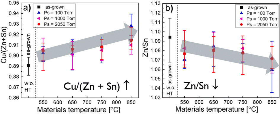 | ||
| Fig. 4 (a) Cu/(Zn + Sn) and (b) Zn/Sn compositional ratios of the CZTS MGP crystals depending on the post-annealing regime as determined by EDX. Reproduced from ref. 34 with permission from Elsevier B.V., Copyright 2022. | ||
This two-step process, which involves etching and annealing, is considered essential in the preparation of CZTS powders for their application as a solar cell absorber material. As a result, this method finds widespread use in all subsequent studies for processing monograin powders.
2.3. Cu–Zn disordering
Defects in semiconductor materials play a significant role in determining their optoelectronic properties. Lattice defects, in particular, are crucial to the application of semiconductors in photovoltaic devices, as they directly impact the generation, separation, and recombination of electron–hole pairs.35 It has been found that CuZn antisite defects have low formation energy and high concentration due to the small atom size and chemical potential difference between Cu and Zn, making the synthesized CZTS always p-type.One of the key challenges in improving the quality of an absorber layer is the precise control of intrinsic defects. Zn and Cu are close neighbours in the periodic table with similar atomic size. Therefore, it is more likely for Zn and Cu to occupy vacancies of counterparts and result in a disordered kesterite structure in CZTS.36 This is usually considered as the main reason for the CuZn and ZnCu antisite defects in the CZTS system.37
Numerous reports have been dedicated to understanding the influence of Cu–Zn disorder on the VOC deficit observed in kesterite-based solar cells.38,39 The beneficial strategy to reduce the Cu–Zn disordering involves implementing a low-temperature post-annealing (LT-PA) process around critical temperature (260 ± 10 °C)40 to induce ordering in the CZTS material. This approach aims to enhance the structural and electronic properties of the CZTS absorber, leading to improved device performance.
An additional low-temperature thermal treatment was also employed after the sulfurization process to decrease the degree of Cu–Zn disordering in the CZTS monograins.41 It was found by a low-temperature photoluminescence (LT-PL) study that decreased Cu–Zn disordering of the crystals led to increased Eg by about 100 meV and changed the radiative recombination from band to tail to band to impurity type. It is important to note that kesterite structures can never be completely ordered or disordered phases (Fig. 5). As a result, even in kesterites that are primarily ordered, there are still regions where the disordered phase predominates. These regions with a lower band gap energy can act as funnels for both charge carriers, promoting recombination. This phenomenon can limit the efficiency of photovoltaic devices based on kesterite materials. On the other hand, in the predominantly disordered phase of kesterite materials, regions with ordered structures and higher band gaps may not encourage more recombination. Instead, these ordered regions can serve as possible barriers for charge carriers, hindering their mobility and reducing device performance.
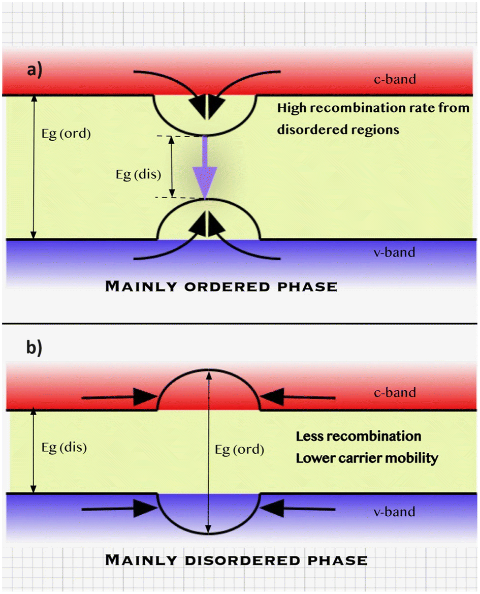 | ||
| Fig. 5 Band structure of (a) mainly ordered CZTS and (b) mainly disordered CZTS. | ||
Extensive investigation was conducted to explore the impact of low-temperature structural ordering in the absorber material on the performance of CZTS monograin layer solar cells.41 Current–voltage (J–V) measurements revealed that the LT-PA resulting in decreased disordering of the CZTS absorber material had a significant impact on the MGL solar cell characteristics; mostly, the values of VOC were increased. The highest VOC of 784 mV was measured for the solar cell based on the powder that was LT-PA at 150 °C for 24 hours. Despite the additional low-temperature heat treatment to reduce Cu–Zn disordering in the CZTS monograins, the VOC deficit remained large compared to the corresponding bandgap values, approximately 520 mV. The moderate LT-PA at 150 °C for 4 hours increased the VOC value by 74 mV giving more than 10% higher efficiency (9.1%) compared to the reference cell (8.1%).41
2.4. Double cation substitution by Cd and Ag
One approach to decrease the occurrence of antisite defects involves substituting Cu (or Zn) with isoelectronic elements having larger covalent radii, such as Ag (or Cd), to elevate the energy barrier for site exchange with Zn. The substitution of Cu with Ag leads to more than a twofold increase in the formation energy of antisite defects, consequently yielding a substantially lower defect density by an order of magnitude.42,43It has also been found that double cation substitution can be employed to enhance device performance beyond what can be achieved with single cation substitution, particularly when the two cations influence the distinct limiting factors of CZTS.44,45 Hadke et al.44 elucidated that the enhanced device efficiencies can be attributed to the introduction of Cd in CZTS, which modifies the defect characteristics of acceptor states near the valence band. Additionally, the incorporation of Ag helps to reduce nonradiative bulk recombination. According to DTF calculations,45 the low levels of Cd doping can suppress disorder in the Cu–Zn sublattice, while low levels of Ag doping only suppress disorder in Cu-rich and constrained Cu-poor conditions. Ag doping in Cu-rich conditions reduces the concentration of Cu vacancies, responsible for CZTS p-type behaviour, and stabilizes the band edge fluctuations. However, excessive Cd or Ag doping can form the stannite structure with a lower band gap.
In monograin technology, a double partial cationic substitution of Cu and Zn was performed by introducing Ag (from 1 to 15% of Cu) and Cd (20% of Zn) into the CZTS lattice. The objective of this substitution was to mitigate CuZn antisite defects and minimize recombination losses.28 We observed significant morphology changes when Ag was added to the mixture of the Cu2(Zn,Cd)SnS4 (CZCdTS) precursor material. The synthesized powder crystals exhibited a transition from sharp-edged tetragonal shapes to more rounded forms (Fig. 6). This alteration in morphology could potentially be attributed to the increased solubility of the formed (Cu,Ag)2(Zn,Cd)SnS4 (ACZCdTS) compound in the flux, in comparison to pure CZCdTS. According to EDX analysis, the content of Ag in the material was found to be variable, with the synthesized powders having an Ag content that remained approximately two times lower than the initial input value. In the investigated compositional region, no structural changes were observed. The presence of the kesterite phase and the tetragonal lattice structure were confirmed through Raman spectroscopy and X-ray diffraction analysis for all the synthesized powders. The observed systematic shift of all diffraction peaks towards lower angles, along with the linear increase in crystal lattice parameters of a and c, was attributed to the substitution of Cu+ with the larger and heavier Ag+ ions.
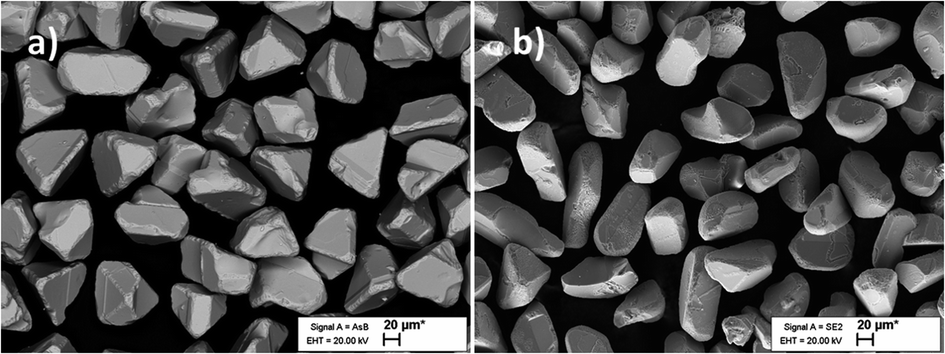 | ||
| Fig. 6 SEM images of (Cu1−x Agx)1.85(Zn0.8Cd0.2)1.1SnS4 monograin powder crystals: (a) x = 0 and (b) x = 0.15. Reproduced from ref. 28 with permission from the Royal Society of Chemistry, Copyright 2019. | ||
From EQE measurements, band gap values were extracted, showing a slight increase from 1.50 eV to 1.53 eV with an increase in Ag content in ACZCdTS monograin powder materials. As the Ag content in ACZCdTS increased, the VOC value increased, but it did not follow the increase in Eg. This suggests that the changes in VOC values resulting from the addition of Ag in CZCdTS cannot be solely explained by variations in the bandgap of the absorber. Instead, they are likely related to changes in the recombination processes.
Temperature and excitation power dependent LT-PL measurements revealed the presence of two distinct radiative recombination mechanisms in all the studied powders (Fig. 7). At low temperatures, a donor–acceptor-pair transition was observed, while at high temperatures, a free-to-bound transition occurred. It was found that the incorporation of Ag into the powder crystals had no effect on the radiative recombination mechanism, although a significant increase in the PL intensity was observed in the Ag-containing materials compared to the reference (Fig. 8). The highest PL signal was obtained from the powder sample containing 1% Ag with respect to Cu, which also resulted in the highest efficiency of 8.73% in the corresponding solar cells.28 The most significant enhancement was observed in the short-circuit current density values (Fig. 9). Since LT-PL analysis showed no change in the radiative recombination mechanism for the studied Ag contents, the observed effects are likely due to the suppression of non-radiative recombination and/or reduction in interface recombination. Temperature-dependent J–V measurements indicated that the dominant recombination mechanism in the studied system is interface recombination. This means that the recombination of charge carriers primarily occurs at the interfaces between different layers or regions within the device structure. For a more in-depth analysis of the solar cell characteristics and to gain insights into the recombination processes, all the light J–V curves were fitted using a two-diode model.46 Although the overall fitting was good, the second diode exhibited unusual fit parameters, such as a relatively high saturation current density (J02) and ideality factor (n2). These unexpected characteristics indicate potential current losses at higher voltages, which are commonly associated with recombination processes or the presence of crystals with poor performance. To comprehend the suggested recombination processes, the relationship between the ideality factor (n1) and temperature was examined.28 The observed temperature dependence of n1 suggested tunnelling enhanced interface recombination. Initially, the tunnelling energy (E00) increased with increasing Ag content, but at the highest Ag concentration (15%), it decreased. The increase in E00 was explained by the higher acceptor concentration due to Ag doping. The optimized Ag content in the CZCdTS absorber material reduced the concentration of CuZn antisite defects, leading to an increase in acceptor defects like CuCd and AgZn, as predicted by DFT studies.43 However, a high concentration of Ag may compensate for these acceptor defects, resulting in reduced carrier density, leading to poor junction formation and a decrease in solar cell performance.
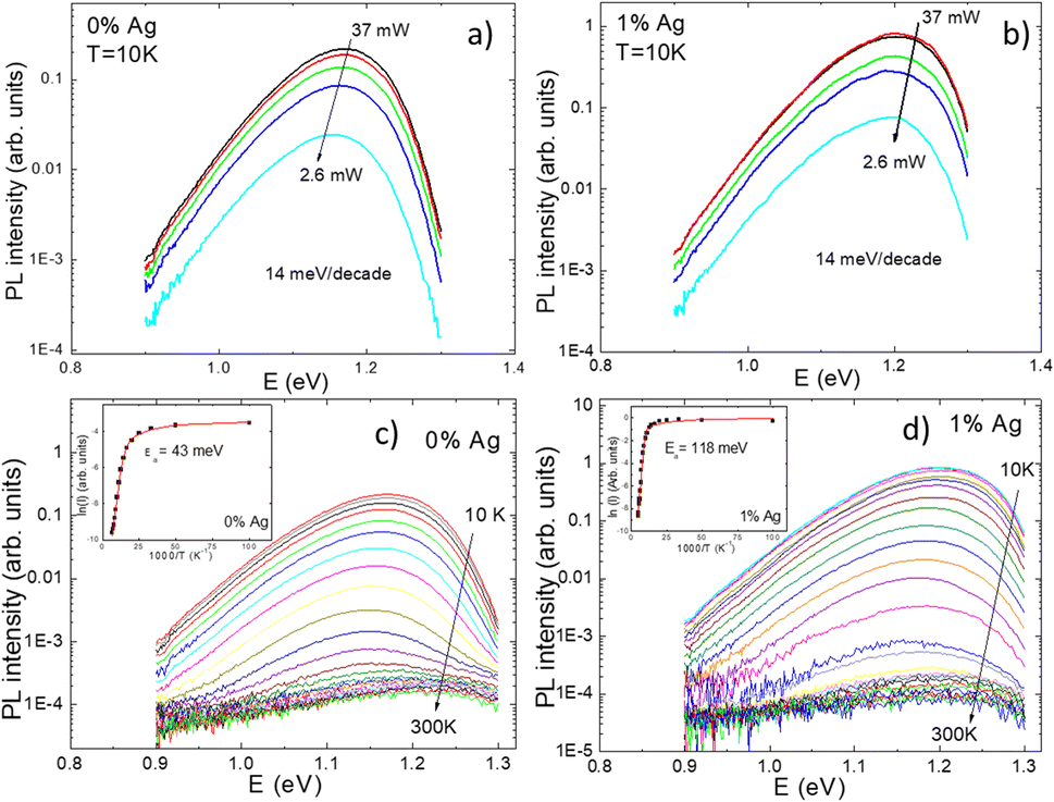 | ||
| Fig. 7 The laser power (a and b) and temperature dependencies (c and d) of the PL spectra for CZCdTS monograin powders with Ag content of 0 at% and 1 at%. The inset graphs present the thermal activation energies derived from the temperature dependencies of the PL spectra. Reproduced from ref. 28 with permission from the Royal Society of Chemistry, Copyright 2019. | ||
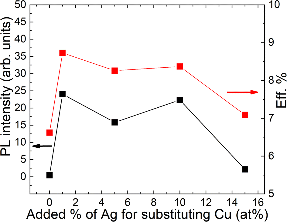 | ||
| Fig. 8 The dependence of PL intensities of monograin powders and power conversion efficiencies of solar cells on the input Ag content. Reproduced from ref. 28 with permission from the Royal Society of Chemistry, Copyright 2019. | ||
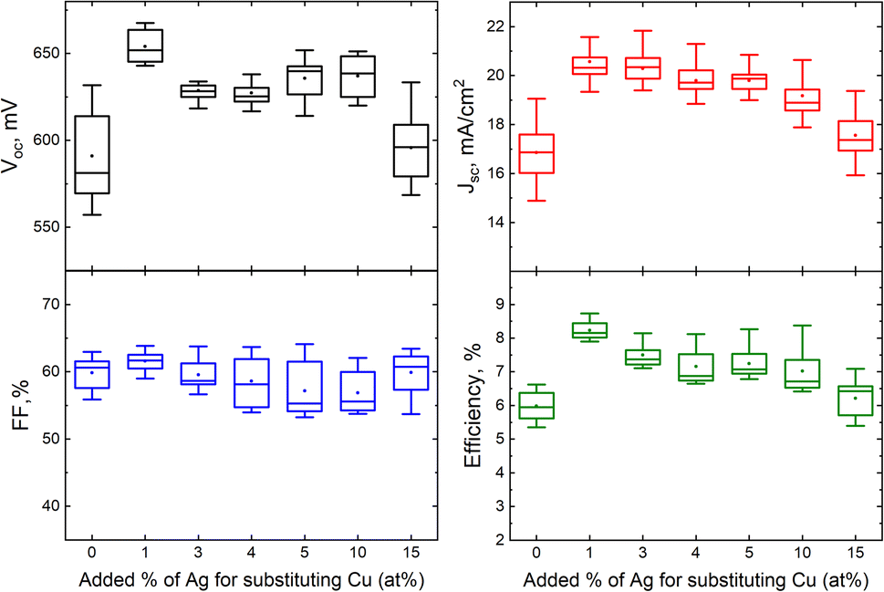 | ||
| Fig. 9 Box plots of open circuit voltage, short-circuit current density, fill factor and efficiency of MGL solar cells fabricated from ACZCTS monograin powders with different added Ag content with respect to Cu. Reproduced from ref. 28 with permission from the Royal Society of Chemistry, Copyright 2019. | ||
Our results confirmed that the beneficial effect of Ag in ACZCTS MGL solar cells is observed only at very low Ag concentrations (1%), while higher levels of Ag prove to be detrimental to solar cell performance. These findings highlight the significance of interface engineering and optimization in mitigating recombination losses and improving the overall performance of the device.
2.5. Co-doping with Li and K
A prospective strategy to improve the PCE of the kesterite solar cells is doping of the absorber material with alkali.47 The positive effect of Li+ incorporation can be attributed to its relatively lower LiCu substitution energy compared to other alkali elements incorporated in the absorber. Nuclear magnetic resonance investigations have revealed that the presence of Li in materials within the kesterite domain tends to reduce the Cu–Zn disorder.48 Alloying with Li offered a way to modify the bandgap and conduction band offset of the CZTS.48,49Monograin powder synthesis involves the use of inorganic halide salts (such as KI, LiI, and mixtures of KI and LiI) in a liquid phase at elevated temperatures. Consequently, unintentional doping of the formed semiconductor crystals occurs with elements present in the salt, such as K, Li, and I. The extent of doping relies on the heating time and temperature and is limited by the solubility of the dopant within the matrix crystal under saturation conditions. It has been observed that the incorporation of Li into kesterite is influenced by the presence of Na. Therefore, achieving Li alloying is more feasible in the absence of Na.50 There were no consistent set of experimental results regarding the influence of constituent elements from salt on the properties of kesterite monograin powders and the performance of monograin solar cell devices. Notably, all high-efficiency CZTS monograin layer solar cells are based on powders synthesized in the presence of KI, which results in the inclusion of potassium in the powders. In the study,32 the effects of co-doping with K and Li on the optoelectronic properties of CZTS monograin powder and device performance were investigated. The levels of extrinsic doping in CZTS powder crystals were adjusted by employing different salt mixtures during the synthesis process.
According to atomic absorption spectroscopy analysis, the concentration of potassium in all synthesized materials was found to be 0.01 at% regardless of the amount of LiI present in the KI flux. This consistent K concentration suggests that the CZTS material reaches a saturation point for K incorporation at the synthesis temperature of 740 °C. However, the concentration of Li varied based on the initial amount of LiI in the LiI–KI flux mixture, ranging from 0.01 at% to 1.22 at% in the synthesized CZTS. When the Li content reached 0.81% or higher in the CZTS material, the formation of a solid solution occurred, resulting in (Cu1−xLix)ZnSnS4.32 The formation of the solid solution was also confirmed by Raman and XRD structural analysis. As the Li concentration increased, the diffraction peaks in CZTS shifted to lower diffraction angles, indicating structural changes in the CZTS lattice due to the incorporation of Li ions. Li has a larger covalent radius compared to Cu and Zn, leading to a longer lithium–sulphur bonding distance when substituting Cu or Zn in the kesterite lattice with Li ions, contributing to the observed shift in the diffraction peaks. Calculated lattice parameters a and c increased also with increasing the Li content in CZTS.
The influence of K and Li co-doping effect on the defect structure and related recombination processes in CZTS monograins were studied by LT-PL. Regardless of the Li content, all PL spectra consisted of at least two asymmetric PL bands (Fig. 10). PL emission of all samples was most probably dominated by the same deep donor–deep acceptor complex. The activation energy EA of the quenching of PL increased with increasing the Li content and this can be an indication that the depth of acceptor defect levels increased with Li concentration. As the lattice parameters of CZTS increased with Li concentration, the distances between possible acceptor and donor defects also increased, leading to the increase of acceptor level ionization energy.
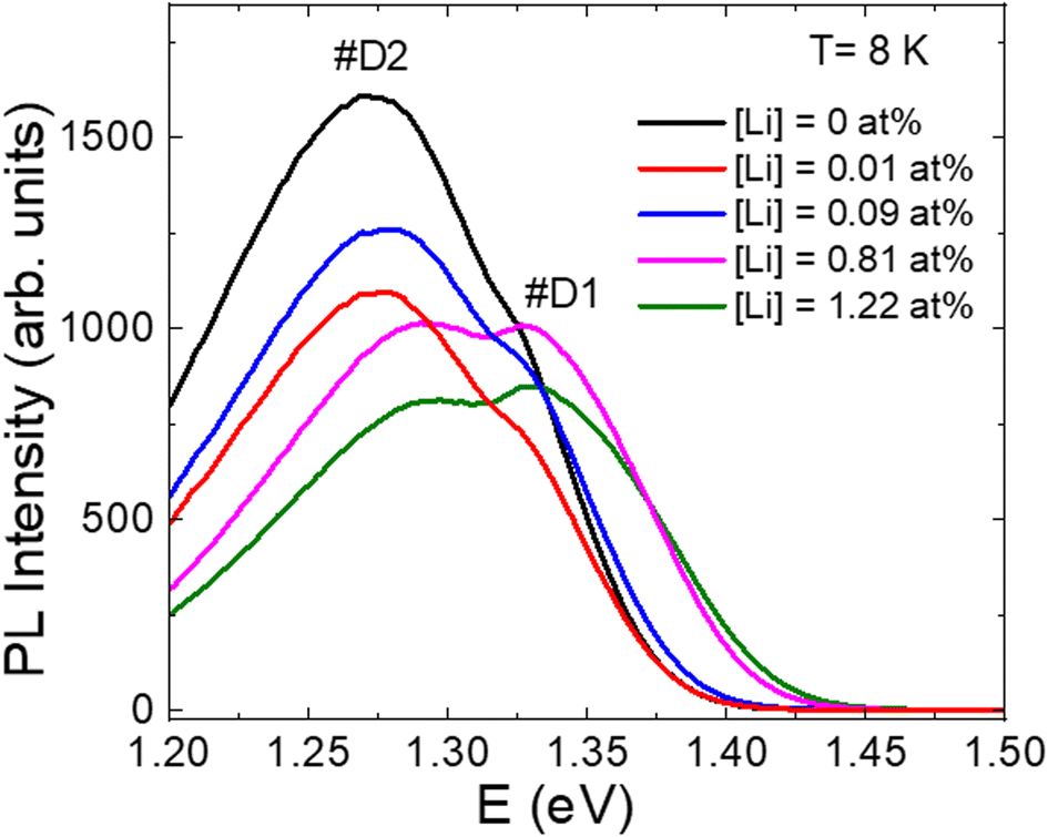 | ||
| Fig. 10 PL spectra of post-annealed CZTS monograins with different Li concentrations in the input composition of CZTS. Reproduced from ref. 32 with permission from Elsevier B.V., Copyright 2023. | ||
The influence of Li on the bandgap of CZTS was investigated using EQE measurements. It was found that CZTS powders with Li content up to 0.09% in the synthesized powders had an effective bandgap (Eg*) of approximately 1.52 eV. However, as the Li content in the final CZTS composition increased to 0.81% or higher, a significant increase in the bandgap of the absorber material was observed, reaching a value of 1.57 eV.
The research results confirmed that CZTS powders synthesized in pure KI flux or in a mixture of less than 1 mol% LiI from the KI flux contained K and Li at the doping level, but further increase of Li led to the formation of a (Cu1−xLix)ZnSnS4 solid solution.
The photovoltaic characteristics showed that the addition of Li into the CZTS absorber had a significant effect on the VOC value, which increased from 721 mV to 784 mV as the Li content in the synthesized CZTS powders was increased from 0% to 1.22% (Fig. 11). While the VOC values increased with Li incorporation, the difference between the measured VOC and the theoretical VSQOC was slightly reduced, approximately by 20 mV. However, this difference (VOC deficit) was still relatively large.
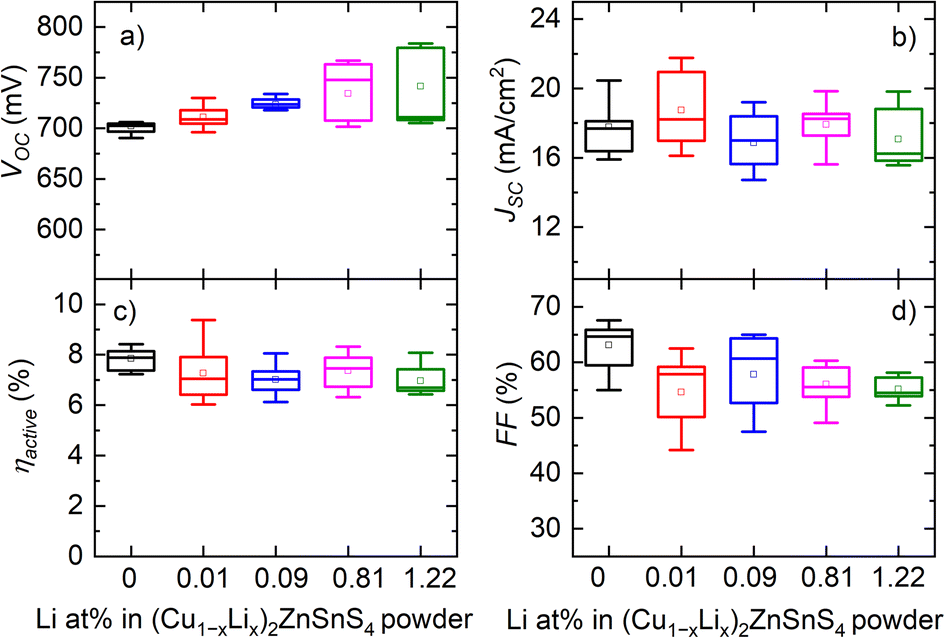 | ||
| Fig. 11 Box-plot diagram of CZTS solar cell parameters (a) open circuit voltage (VOC), (b) current density (JSC), (c) efficiency (ηactive) and (d) fill factor (FF) with different Li concentrations in the CZTS powder. Reproduced from ref. 32 with permission from Elsevier B.V., Copyright 2023. | ||
The highest efficiency achieved for the monograin layer solar cell was 9.4% using the absorber material co-doped with both K and Li at a level of 0.01 at% in the synthesized CZTS.32
2.6. Buffer layer and absorber/buffer interface
In all the previously mentioned studies, the preparation of powders as absorbers involved the use of chemical and thermal treatments. Subsequently, these prepared powders were coated with a CdS buffer layer using the chemical bath deposition (CBD) method. CZTS powders were subjected to the deposition of the CdS buffer layer by CBD using a vertical rotator in a hot-air thermostat at 60 °C for 20 min. The 360° multifunctional vertical rotator provides compact and uniform CdS coverage on CZTS crystals. CBD involves immersion of the post-treated CZTS powders in a solution containing 0.01 M cadmium iodide (CdI2), 1 M thiourea (SC(NH2)2), and 2 M ammonia aqueous solution (NH4OH). The thickness of the CdS buffer layer is ∼45 nm using the above-mentioned processing conditions.CZTS solar cells exhibit a negative band offset, often referred to as a “cliff-like” band alignment, where the conduction band minimum (CBM) of CZTS is higher than that of CdS. This negative conduction band offset (CBO) has been found to limit the VOC and FF due to recombination at the heterojunction interface.51,52 Addressing the challenges associated with the CZTS/CdS interface is crucial for improving the efficiency of CZTS solar cells.
In monograin technology, a specific step involves the air annealing of CdS-covered CZTS powders at temperatures ranging from 200 to 225 °C immediately after the deposition of the buffer layer.12 The post-deposition soft-annealing (PDT) process applied to the CZTS/CdS interface demonstrated several effects on the material and interface properties. It reduced the degree of Cu–Zn disordering within the CZTS material. By promoting a more ordered crystal structure, the band gap of CZTS increased from 1.57 to 1.62 eV by prolonging the annealing time to 2 hours. However, this process also increased recombination losses at the interface, and resulted in the formation of a Cu-rich CZTS surface ([Cu]/([Zn] + [Sn]) > 1). The out-diffusion of Cu from the absorber layer is a well-known phenomenon that occurs in the Cu-chalcogenide/CdS heterojunction.53 The accumulation of Cu at the interface can create a localized region with a higher concentration of Cu. This Cu-rich region may have different electronic properties compared to the rest of the absorber layer, potentially affecting the overall device performance. The presence of Cu at the interface can also lead to diffusion of Cu into CdS, which increased the photoconductivity of CdS and increased the series resistance (RS) of devices. Another effect of the PDT treatment is the diffusion of Cd from the CdS layer into the surface of CZTS. This diffusion process leads to the formation of an ultra-thin layer of Cu2ZnxCd1−xSnS4 at the CZTS surface, which affected the interface properties and electronic band alignment between CZTS and CdS. These findings highlight the complex interplay of material and interface properties in the CZTS/CdS system and the impact of PDT treatment.
In summary, PDT treatment in the CZTS/CdS system has shown both positive and negative effects on the material and interface properties. It reduced Cu–Zn disordering and increased the band gap of CZTS, which were beneficial for solar cell performance. However, it also leads to increased recombination losses at the interface and the formation of a Cu-rich CZTS surface, which can negatively impact device performance.
Achieving an optimal balance between Cu–Zn disorder reduction, minimizing recombination losses, and managing compositional changes is crucial for maximizing the performance of CZTS solar cells. Therefore, we further applied the two-step heterojunction formation process by controlling the intermixing of Cd and Cu at the CZTS/CdS interface. In addition to the CdS annealing step, an additional process was implemented where the CdS layer was removed using concentrated hydrochloric acid (HCl). After the removal of CdS, a fresh CdS buffer layer was deposited on the CZTS crystals without undergoing any additional post-annealing treatment.20 The combined process for heterojunction formation slightly improved VOC values from 723 to 735 mV; the main improvement was in JSC from 20.5 to 23.6 mA cm−2, and in FF from 59.4% to 67.7%. The RS of the monograin layer solar cells based on the CZTS-modified absorber was significantly reduced from 2.4 Ω cm2 to 0.67 Ω cm2. As a result, enhanced device performance with PCE of 11.7% was obtained.20 The electrical behaviour of the high efficiency CZTS monograin layer solar cell was investigated through temperature-dependent J–V characteristics.20 Dark J–V curves were fitted using a two-diode model and the light curves were analysed using the single exponential diode equation.20,46 To gain a deeper understanding of the non-ideal behavior of the solar cell, a more detailed analysis was conducted on the diode ideality factor (n), series resistance (RS), and parallel shunt resistance (RSH). From the room temperature dark curve fitting, the ideality factor values for the two diodes were determined to be 1.62 and 3.3, respectively. The significantly higher value of 3.3 for the second diode (n2) suggested the presence of a tunnelling component in its behavior. The temperature dependence of RS exhibited a straightforward exponential relationship for both light and dark conditions, with activation energies of Ea = 59 meV and Ea = 99 meV, respectively. Typically, this activation energy is attributed to the back-contact barrier height and impacts the solar cell performance, leading to relatively low values of FF. The difference between the activation energies observed in the dark and light cases suggests the presence of weak photoconductivity.
At higher temperatures, the RSH in the light curves showed nearly linear growth, resulting in smaller current losses compared to lower temperatures. This ohmic behavior of RSH is likely due to ohmic shunts caused by pinholes in the polymer layer between crystals or low-resistance grain boundaries. Conversely, at low temperatures, RSH increased exponentially, with Ea of ∼20 meV, potentially associated with shallow trap levels in the CdS buffer layer. Interestingly, RSH values obtained from dark curves were about 1000 times higher than those from light curves. This significant decrease in RSH with illumination suggests strong influence from illumination and likely links to the buffer layer's photoconductivity. The CdS layer covers the crystals while they are embedded into the polymer layer. During the back-contact formation process, the CdS layer is typically removed from the back side by etching and mechanical polishing. However, there is a low probability that some remains of the CdS layer might still come into contact with the back contact.
By fine-tuning various parameters in the monograin technology process and by implementing the best available technological techniques, a slight improvement in the efficiency of the solar cells has been achieved, resulting in an efficiency of 12.06% with output parameters VOC = 745 mV, JSC = 28.36 mA cm−2 and FF = 57.1% (Fig. 12).
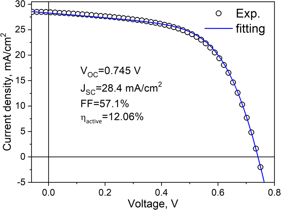 | ||
| Fig. 12 Current density–voltage curve of the record efficiency CZTS MGL solar cell. | ||
The J–V data analysis revealed that the primary recombination mechanism, such as tunnelling-enhanced interface recombination, remained dominant in the record efficiency CZTS monograin layer solar cells. Hence, addressing the challenges associated with back contact barriers, recombination mechanisms, and shunts remains an important area for future research and optimization of CZTS monograin layer solar cells.
2.7. Flexible CZTS monograin layer solar cells
Considering all the previous studies, we extended our investigation to fabricate flexible solar cells and performed a statistical comparison of their output parameters with devices made on a rigid substrate. This comparison aimed to assess the performance of the flexible monograin layer solar cells and understand any potential differences or advantages they may offer over the rigid substrate-based devices. The findings from this comparison could provide valuable insights into the feasibility and practicality of utilizing flexible CZTS solar cells for specific applications and pave the way for future advancements in this field. Fig. 13 shows two MGL solar cells – one is glued on the glass (rigid) and the other on the Translux ETFE (ethylene tetrafluoroethylene) substrate (flexible). The choice to compare ETFE film to glass was primarily driven by the fact that the ETFE film demonstrated similar transmittance characteristics. This made it a suitable candidate for evaluation as a potential alternative substrate for the MGL solar cells, offering comparable performance to glass while providing the added advantage of flexibility. Fig. 14 displays the voltage maps of the 2.5 cm × 2.5 cm device area acquired from two types of MGL solar cells: (a) the rigid MGL solar cells and (b) the flexible MGL solar cells with an Au contact size of 0.018 mm2. On the right side of the figure, the oval Ag front contact is shown (in grey color), and the Au back contacts are shown as hexagonal shapes.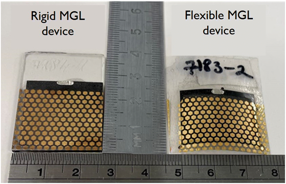 | ||
| Fig. 13 MGL device on the glass substrate (left) and on the polymer substrate (right). | ||
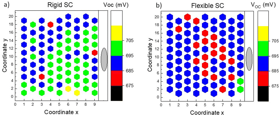 | ||
| Fig. 14 Map of the VOC over the 2.5 cm × 2.5 cm area obtained from (a) the rigid MGL solar cell and (b) flexible MGL solar cell (contact size 0.018 mm2). | ||
The measured VOC values of the rigid device range from 679 mV to 706 mV, with a mean value of 695 mV. The percentage deviation being within ±2.3% of the mean suggests a quite stable and consistent performance in terms of VOC. The flexible MGL solar cell, on the other hand, displays slightly less variation in its VOC results. The VOC values range from 681 mV to 701 mV, which fall within ±2% of the mean value. The mean VOC for the flexible device is measured at 687 mV. These results indicate similar stability in performance for the flexible MGL solar cells. The FF and JSC values obtained in both types of devices varied from 49% to 61% and 13 to 26 mA cm−2, respectively. The significant variation in values can be attributed to the spatial distribution of contacts in the solar cell. The outermost and corner contacts are situated farther from the front contact, leading to increased resistance and reduced surface conductivity in those regions. To address this issue and improve the current collection efficiency, it is essential to incorporate current collecting grids and/or highly conductive Ag nanowires54 on the front side of the solar cell. Fig. 15 shows the J–V characteristics of both the best performing rigid and flexible CZTS MGL solar cells. Notably, there is no significant efficiency gap between the CZTS monograin layer solar cells fabricated using flexible and rigid substrates. This finding is promising as it indicates that the flexibility of the substrate does not compromise the overall efficiency of the CZTS MGL solar cells, making them suitable candidates for various applications regardless of the substrate type. However, conducting bending and mechanical tests on the monograin layer solar cells is essential to ensure their suitability for use on surfaces with various curvatures and in applications that involve repeated bending. These tests will provide valuable insights into the structural integrity, durability, and reliability of the solar cells under such conditions. By thoroughly evaluating their performance, we can optimize and enhance the design to meet the demands of flexible applications, advancing the practicality and feasibility of monograin layer solar cell technologies.
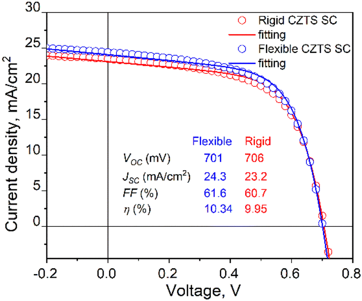 | ||
| Fig. 15 J–V curves of rigid and flexible CZTS monograin layer solar cells. | ||
3. Conclusions
This review provides a comprehensive overview of the significant advancements made in pure sulfide kesterite monograin powder technology and its applications in solar cells over the past decade. Based on the extensive research and findings presented, several key conclusions can be drawn.High-purity CZTS monograin powders are produced through a reaction of CuS, ZnS, and SnS in potassium iodide flux. Compositional ratios of Cu/(Zn + Sn) = 0.91 and Zn/Sn = 1.08 achieve high-efficiency CZTS monograin layer solar cells. The two-step etching and annealing process during post-annealing increases the ratio of Cu/(Zn + Sn) in the bulk while decreasing the Zn/Sn ratio. This improves CZTS powder quality for solar cell applications.
Various strategies were explored to improve the VOC losses in CZTS monograin layer solar cells. These included reducing the Cu–Zn disordering, as well as doping and alloying with other elements. The results indicated that low-temperature post-annealing was effective in reducing Cu–Zn disordering, leading to an increase in Eg by approximately 100 meV. However, it was concluded that kesterite structures cannot be entirely ordered or disordered phases. Even in primarily ordered kesterites, regions with disordered phases still coexist. These regions with lower Eg can act as charge carrier funnels, promoting recombination, which negatively impacts the efficiency of photovoltaic devices based on kesterite materials. On the other hand, predominantly disordered phases might not encourage more recombination, as regions with ordered structures and higher band gaps could act as barriers, hindering charge carrier mobility and reducing the overall performance of the devices. Therefore, achieving the optimal balance between ordered and disordered regions in kesterite materials is crucial for enhancing the performance of photovoltaic devices.
Through double cation substitution, non-radiative recombination was suppressed, and the short-circuit current density of solar cells was increased. In particular, optimizing the Ag content (at 1%) in the CZCdTS absorber material reduced the concentration of CuZn antisite defects, leading to an increase in acceptor defects like CuCd and AgZn. However, a high concentration of Ag had a compensating effect on these acceptor defects, resulting in reduced carrier density, poor junction formation, and a decrease in solar cell performance.
The research findings on co-doping of Li and K in CZTS powders demonstrated that when the powders were synthesized in pure KI flux or with a mixture of less than 1 mol% LiI from KI flux, K and Li were present at the doping level. However, increasing the Li content further resulted in the formation of a (Cu1−xLix)ZnSnS4 solid solution. This led to a significant increase in the bandgap of the absorber material, reaching a value of 1.57 eV, and improved VOC from 721 mV to 784 mV. However, the difference between measured VOC and theoretical VSQOC was still relatively large, suggesting further optimization is needed.
The most effective performance improvement was achieved through heterojunction modifications. Soft-annealing of CZTS/CdS had both positive and negative effects on the material and interface properties. It reduced Cu–Zn disordering and increased the band gap of CZTS, benefiting solar cell performance. However, it also led to increased recombination losses at the interface and the formation of a Cu-rich CZTS surface, which could negatively impact device performance. The combined process for heterojunction formation resulted in slight improvements in VOC values, while the main enhancements were observed in JSC and FF, leading to an overall efficiency of 12.06% for the CZTS-based solar cells. Moreover, the series resistance (RS) of the monograin layer solar cells based on the CZTS-modified absorber significantly decreased.
The detailed J–V data analysis revealed that the primary recombination mechanism, such as tunnelling-enhanced interface recombination, remained dominant in the record efficiency CZTS monograin layer solar cells. Hence, addressing the challenges associated with back contact barriers, recombination mechanisms, and shunts remains an important area for future research and optimization of CZTS monograin layer solar cells.
The comparative experiments conducted on rigid and flexible devices within this research provide promising results, suggesting that monograin layer technology holds great potential for diverse applications in the future.
Author contributions
M. K.-K.: conceptualization, writing – original draft, writing – review & editing, formal analysis, resources. K. T., M. P., and K. M.: investigation, methodology, formal analysis. V. M., R. J. and M. D.: investigation, formal analysis. J. K.: writing – review & editing, formal analysis, methodology. M. G.-K.: writing – review & editing, formal analysis, methodology, funding acquisition, project administration.Conflicts of interest
The authors declare no conflict of interest.Acknowledgements
This work was supported by the European Union's H2020 research and innovation programme under Grant Agreement No. 952982, and by the Estonian Research Council Grants PRG1023 and TT13.References
- W. Liu, Y. Liu, Z. Yang, C. Xu, X. Li, S. Huang, J. Shi, J. Du, A. Han, Y. Yang and G. Xu, et al. , Nature, 2023, 617, 717–723 CrossRef CAS PubMed.
- Flexible solar cells with record efficiency of 22.2%, https://www.empa.ch/web/s604/solarzellen-rekord?inheritRedirect=true Search PubMed.
- M. Jahandar, A. Prasetio, C. Lee, H. Kim, A. R. Kim, J. Heo, Y. Kim, S. Kim and D. C. Lim, Chem. Eng. J., 2022, 448, 137555 CrossRef CAS.
- Y. Gao, K. Huang, C. Long, Y. Ding, J. Chang, D. Zhang, L. Etgar, M. Liu, J. Zhang and J. Yang, ACS Energy Lett., 2022, 7, 1412–1445 CrossRef CAS.
- K. Timmo, M. Altosaar, M. Kauk, J. Raudoja and E. Mellikov, Thin Solid Films, 2007, 515, 5884–5886 CrossRef CAS.
- M. Kauk-Kuusik, X. Li, M. Pilvet, K. Timmo, M. Grossberg, T. Raadik, M. Danilson, V. Mikli, M. Altosaar, J. Krustok and J. Raudoja, Thin Solid Films, 2018, 666, 15–19 CrossRef CAS.
- K. Muska, M. Kauk, M. Altosaar, M. Pilvet, M. Grossberg and O. Volobujeva, Energy Proc., 2011, 10, 203–207 CrossRef CAS.
- F. Ghisani, K. Timmo, M. Altosaar, V. Mikli, M. Pilvet, R. Kaupmees, J. Krustok, M. Grossberg and M. Kauk-Kuusik, Thin Solid Films, 2021, 739, 138980 CrossRef CAS.
- K. Timmo, M. Kauk-Kuusik, M. Pilvet, V. Mikli, E. Kärber, T. Raadik, I. Leinemann, M. Altosaar and J. Raudoja, Phys. Status Solidi C, 2016, 13, 8–12 CrossRef CAS.
- D. Meissner, K. Ernits, S. Gahr, L. Kapitan, M. Vetter, C. Glatz and R. Syed, Sol. Energy Mater. Sol. Cells, 2023, 252, 112160 CrossRef CAS.
- C. Platzer-Björkman, N. Barreau, M. Bär, L. Choubrac, L. Grenet, J. Heo, T. Kubart, A. Mittiga, Y. Sanchez, J. Scragg, S. Sinha and M. Valentini, JPhys Energy, 2019, 1, 044005 CrossRef.
- M. Kauk-Kuusik, K. Timmo, K. Muska, M. Pilvet, J. Krustok, R. Josepson, G. Brammertz, B. Vermang, M. Danilson and M. Grossberg, ACS Appl. Energy Mater., 2021, 4, 12374–12382 CrossRef CAS.
- M. Grossberg, J. Krustok, C. J. Hages, D. M. Bishop, O. Gunawan, R. Scheer, S. M. Lyam, H. Hempel, S. Levcenco and T. Unold, JPhys Energy, 2019, 1, 044002 CrossRef CAS.
- M. A. Green, E. D. Dunlop, M. Yoshita, N. Kopidakis, K. Bothe, G. Siefer and X. Hao, Prog. Photovoltaics Res. Appl., 2023, 31, 651–663 CrossRef.
- S. Kim, J. A. Márquez, T. Unold and A. Walsh, Energy Environ. Sci., 2020, 13, 1481–1491 RSC.
- W. Shockley and H. J. Queisser, J. Appl. Phys., 1961, 32, 510–519 CrossRef CAS.
- A. D. Collord and H. W. Hillhouse, Chem. Mater., 2016, 28, 2067–2073 CrossRef CAS.
- J. Zhou, X. Xu, H. Wu, J. Wang, L. Lou, K. Yin, Y. Gong, J. Shi, Y. Luo, D. Li, H. Xin and Q. Meng, Nat. Energy, 2023, 8, 526–535 CrossRef CAS.
- M. Nakamura, K. Yamaguchi, Y. Kimoto, Y. Yasaki, T. Kato and H. Sugimoto, IEEE J. Photovoltaics, 2019, 9, 1863–1867 Search PubMed.
- M. Kauk-Kuusik, K. Timmo, K. Muska, M. Pilvet, J. Krustok, M. Danilson, V. Mikli, R. Josepson and M. Grossberg-Kuusk, JPhys Energy, 2022, 4, 024007 CrossRef.
- C. Neubauer, E. Babatas and D. Meissner, Appl. Surf. Sci., 2017, 423, 465–468 CrossRef CAS.
- M. Altosaar, J. Raudoja, K. Timmo, M. Danilson, M. Grossberg, J. Krustok and E. Mellikov, Phys. Status Solidi, 2008, 205, 167–170 CrossRef CAS.
- M. Kauk-Kuusik, K. Timmo, M. Danilson, M. Altosaar, M. Grossberg and K. Ernits, Appl. Surf. Sci., 2015, 357, 795–798 CrossRef CAS.
- K. Timmo, M. Altosaar, J. Raudoja, K. Muska, M. Pilvet, M. Kauk, T. Varema, M. Danilson, O. Volobujeva and E. Mellikov, Sol. Energy Mater. Sol. Cells, 2010, 94, 1889–1892 CrossRef CAS.
- K. Muska, M. Kauk, M. Grossberg, M. Altosaar, J. Raudoja and O. Volobujeva, Energy Proc., 2011, 10, 323–327 CrossRef CAS.
- M. Kauk-Kuusik, M. Altosaar, K. Muska, M. Pilvet, J. Raudoja, K. Timmo, T. Varema, M. Grossberg, E. Mellikov and O. Volobujeva, Thin Solid Films, 2013, 535, 18–21 CrossRef CAS.
- M. Kauk, K. Muska, M. Altosaar, J. Raudoja, M. Pilvet, T. Varema, K. Timmo and O. Volobujeva, Energy Proc., 2011, 10, 197–202 CrossRef CAS.
- K. Timmo, M. Altosaar, M. Pilvet, V. Mikli, M. Grossberg, M. Danilson, T. Raadik, R. Josepson, J. Krustok and M. Kauk-Kuusik, J. Mater. Chem. A, 2019, 7, 24281–24291 RSC.
- J. Krustok, T. Raadik, R. Kaupmees, M. Grossberg, M. Kauk-Kuusik, K. Timmo and A. Mere, J. Phys. D Appl. Phys., 2019, 52, 285102 CrossRef CAS.
- M. Pilvet, M. Kauk-Kuusik, M. Grossberg, T. Raadik, V. Mikli, R. Traksmaa, J. Raudoja, K. Timmo and J. Krustok, J. Alloys Compd., 2017, 723, 820–825 CrossRef CAS.
- M. Pilvet, M. Kauk-Kuusik, M. Altosaar, M. Grossberg, M. Danilson, K. Timmo, A. Mere and V. Mikli, Thin Solid Films, 2015, 582, 180–183 CrossRef CAS.
- K. Muska, K. Timmo, M. Pilvet, R. Kaupmees, T. Raadik, V. Mikli, M. Grossberg-Kuusk, J. Krustok, R. Josepson, S. Lange and M. Kauk-Kuusik, Sol. Energy Mater. Sol. Cells, 2023, 252, 112182 CrossRef CAS.
- K. Timmo, M. Altosaar, J. Raudoja, M. Grossberg, M. Danilson, O. Volobujeva and E. Mellikov, in 2010 35th IEEE Photovoltaic Specialists Conference, IEEE, 2010, pp. 001982–001985 Search PubMed.
- K. Timmo, M. D. Sadurni, M. Pilvet, K. Muska, M. Altosaar, V. Mikli, F. Atlan, M. Guc, V. Izquierdo-Roca, M. Grossberg-Kuusk and M. Kauk-Kuusik, Sol. Energy Mater. Sol. Cells, 2023, 250, 112090 CrossRef CAS.
- S. Chen, A. Walsh, X.-G. Gong and S.-H. Wei, Adv. Mater., 2013, 25, 1522–1539 CrossRef CAS PubMed.
- S. Schorr, Sol. Energy Mater. Sol. Cells, 2011, 95, 1482–1488 CrossRef CAS.
- S. Chen, X. G. Gong, A. Walsh and S.-H. Wei, Appl. Phys. Lett., 2009, 94, 41903 CrossRef.
- J. K. Larsen, J. J. S. Scragg, N. Ross and C. Platzer-Björkman, ACS Appl. Energy Mater., 2020, 3, 7520–7526 CrossRef CAS.
- S. Bourdais, C. Choné, B. Delatouche, A. Jacob, G. Larramona, C. Moisan, A. Lafond, F. Donatini, G. Rey, S. Siebentritt, A. Walsh and G. Dennler, Adv. Energy Mater., 2016, 6, 1502276 CrossRef.
- J. J. S. Scragg, L. Choubrac, A. Lafond, T. Ericson and C. Platzer-Björkman, Appl. Phys. Lett., 2014, 104, 41911 CrossRef.
- K. Timmo, M. Kauk-Kuusik, M. Pilvet, T. Raadik, M. Altosaar, M. Danilson, M. Grossberg, J. Raudoja and K. Ernits, Thin Solid Films, 2017, 633, 122–126 CrossRef CAS.
- E. Chagarov, K. Sardashti, A. C. Kummel, Y. S. Lee, R. Haight and T. S. Gershon, J. Chem. Phys., 2016, 144, 104704 CrossRef PubMed.
- Z.-K. Yuan, S. Chen, H. Xiang, X.-G. Gong, A. Walsh, J.-S. Park, I. Repins and S.-H. Wei, Adv. Funct. Mater., 2015, 25, 6733–6743 CrossRef CAS.
- S. H. Hadke, S. Levcenko, S. Lie, C. J. Hages, J. A. Márquez, T. Unold and L. H. Wong, Adv. Energy Mater., 2018, 8, 1802540 CrossRef.
- G. Sai Gautam, T. P. Senftle and E. A. Carter, Chem. Mater., 2018, 30, 4543–4555 CrossRef CAS.
- S. Suckow, T. M. Pletzer and H. Kurz, Prog. Photovoltaics Res. Appl., 2014, 22, 494–501 CrossRef.
- Y. E. Romanyuk, S. G. Haass, S. Giraldo, M. Placidi, D. Tiwari, D. J. Fermin, X. Hao, H. Xin, T. Schnabel, M. Kauk-Kuusik, P. Pistor, S. Lie and L. H. Wong, JPhys Energy, 2019, 1, 044004 CrossRef CAS.
- A. Lafond, C. Guillot-Deudon, J. Vidal, M. Paris, C. La and S. Jobic, Inorg. Chem., 2017, 56, 2712–2721 CrossRef CAS PubMed.
- Y. Yang, X. Kang, L. Huang and D. Pan, ACS Appl. Mater. Interfaces, 2016, 8, 5308–5313 CrossRef CAS PubMed.
- Y. Yang, L. Huang and D. Pan, ACS Appl. Mater. Interfaces, 2017, 9, 23878–23883 CrossRef CAS PubMed.
- M. Bär, B.-A. Schubert, B. Marsen, S. Krause, S. Pookpanratana, T. Unold, L. Weinhardt, C. Heske and H.-W. Schock, Appl. Phys. Lett., 2011, 99, 152111 CrossRef.
- F. Liu, C. Yan, J. Huang, K. Sun, F. Zhou, J. A. Stride, M. A. Green and X. Hao, Adv. Energy Mater., 2016, 6, 1600706 CrossRef.
- J.-F. Guillemoles, L. Kronik, D. Cahen, U. Rau, A. Jasenek and H.-W. Schock, J. Phys. Chem. B, 2000, 104, 4849–4862 CrossRef CAS.
- S. Edinger, N. Bansal, A. R. Wibowo, N. Winkler, P. Illich, A. Zechmeister, L. Plessing, D. Meissner and T. Dimopoulos, Prog. Photovoltaics Res. Appl., 2019, 27, 547–555 CrossRef CAS.
| This journal is © The Royal Society of Chemistry 2023 |