
Low-cost and high-performance selenium indoor photovoltaics†
Zhouqing
Wei
 ab,
Wenbo
Lu
ab,
Zongbao
Li
c,
Mingjie
Feng
a,
Bin
Yan
a,
Jin-Song
Hu
ab and
Ding-Jiang
Xue
*ab
ab,
Wenbo
Lu
ab,
Zongbao
Li
c,
Mingjie
Feng
a,
Bin
Yan
a,
Jin-Song
Hu
ab and
Ding-Jiang
Xue
*ab
aBeijing National Laboratory for Molecular Sciences (BNLMS), CAS Key Laboratory of Molecular Nanostructure and Nanotechnology, Institute of Chemistry, Chinese Academy of Sciences, Beijing 100190, China. E-mail: djxue@iccas.ac.cn
bUniversity of Chinese Academy of Sciences, Beijing 100049, China
cSchool of Materials Science and Engineering, Wuhan Textile University, Wuhan 430200, China
First published on 3rd October 2023
Abstract
Selenium (Se), as the world's oldest photovoltaic material, has reemerged as a promising absorber material for indoor photovoltaics (IPVs) due to its suitable wide bandgap of ∼1.9 eV, nontoxicity, and excellent inherent stability. However, despite the low material cost of Se, conventional high-performance Se photovoltaic devices usually employ high-cost Au as the electrode, significantly increasing the cost of Se-based devices and restricting their future commercialization. Here we replace high-cost Au with low-cost Cu as the electrode, reducing the cost of Se devices by about one order of magnitude. We further introduce an isolation layer of MoOx between Se and Cu films; this prevents the reaction between Se and Cu to form CuSe during the thermal evaporation of Cu, which significantly lowers the device performance. The resulting Se cells achieve an efficiency of 10.4% under indoor illumination at 500 lux, comparable to that of Au electrode-based Se devices and superior to that of the current IPV industry standard of commercialized amorphous silicon cells with indoor photovoltaic efficiency below 10%. Unencapsulated devices also exhibit negligible efficiency loss after 1000 h of storage under ambient conditions.
1. Introduction
As the world's first solid-state solar cells fabricated in 1883, selenium (Se) cells initiated modern photovoltaic research.1–3 After this, Se was extensively investigated as a photovoltaic material, simultaneously stimulating the broader exploration of photovoltaic materials.4–6 These early studies finally resulted in the emergence of silicon (Si) solar cells reported in 1954, laying the foundation for the modern photovoltaic industry.7 However, the bandgap of Se (∼1.9 eV) is too large for single-absorber solar cells, showing a low Shockley–Queisser (S–Q) efficiency limit of ∼23% under standard AM1.5G illumination, compared to the suitable bandgap of Si (∼1.12 eV).8–14 The research on Se photovoltaics thereby gradually declined with the rapidly expanding Si photovoltaic industry.Recently, Se has regained great interest as an ideal candidate for indoor photovoltaics (IPVs) with the recent rapid development of the Internet of Things (IoT), since the absorption spectrum of Se perfectly matches the emission spectra of widely used indoor light sources such as light-emitting diodes (LEDs) and fluorescent lamps (FLs).15–17 This enables that the wide bandgap of Se is just located in the optimum bandgap range from 1.8 to 1.9 eV for IPVs, endowing a high indoor S–Q limit of above 55% for Se IPVs under indoor illumination.15 Se photovoltaic cells have recently achieved an impressive power conversion efficiency (PCE) of 15.1% under indoor illumination at 1000 lux;15 the resulting Se modules have successfully powered a radio-frequency identification-based localization tag under indoor light, realizing a self-powered system with no need to charge or replace batteries.15 Furthermore, the nontoxicity, earth abundance, and intrinsic environmental stability of Se make it ideal for IPV applications.
Besides, Se possesses an advantage of low material cost. The price of elemental Se is as low as 33 $ per kg according to the SHMET website.18 This means that the material cost of a Se film is only about 0.32 $ per m2 with a thickness of 2 μm, which is thick enough for the absorption of incident light considering its high absorption coefficient of above 105 cm−1.17 Furthermore, the impressively high vapor pressure of Se arising from its low melting point of 217 °C makes it ideal for thermal evaporation deposition for fabricating high-quality Se films,17 a high-throughput, low manufacturing cost, and reliable deposition method that has been successfully applied in the industrial manufacturing of Se thin-film photodetectors.19 However, the current most high-efficiency Se devices usually rely on the use of costly noble metal electrodes such as Au electrodes.9,13,15 This suggests that the high cost of metal electrodes would be a critical concern for the future commercialization of Se IPVs. Hence, replacing the high-cost Au electrode with low-cost electrode materials is imperative for the future commercialization of Se IPVs.
Here we replace the high-cost Au electrode widely used in conventional high-performance Se photovoltaic devices with low-cost Cu, reducing the cost of Se devices by about one order of magnitude. We find that the thermally evaporated Cu reacts with Se to form CuSe at the surface of the Se/Cu device during the thermal evaporation of Cu. This significantly lowers the device performance. We thereby add an isolation layer of MoOx between Se and Cu films to avoid the direct contact of Se and Cu and prevent their reaction. The resulting Se cells display a PCE of 10.4% under indoor illumination at 500 lux; this is comparable to that of Au electrode-based Se devices and superior to that of the current IPV industry standard of commercialized amorphous silicon cells with indoor photovoltaic efficiency below 10%. Unencapsulated devices also exhibit negligible efficiency loss after 1000 h of storage under ambient conditions, demonstrating the durable isolation effect of the MoOx layer.
2. Experimental section
2.1 Photovoltaic device fabrication
FTO-coated glass served as the substrate for depositing devices and was cleaned in ultrasonic baths containing detergent, acetone, and isopropanol for 20 min each in sequence. The substrates were blow-dried using highly pure nitrogen, followed by the UV-ozone treatment for 10 min. A TiO2 buffer layer was deposited on FTO glass via spray pyrolysis, and was placed on a hotplate at 450 °C in an air atmosphere, using a mixture of titanium diisopropoxide bis(acetylacetonate) (75% weight% in isopropanol, Alladin) and absolute ethanol in a volume ratio of 1![[thin space (1/6-em)]](https://www.rsc.org/images/entities/char_2009.gif) :9 as a precursor. The film was annealed at 500 °C for 30 minutes and then cooled down naturally. The modification layer (Te), absorption layer (Se), and isolation layer (MoOx) (99.999%, Alfa Aesar) were then deposited onto an FTO/TiO2 substrate by thermal evaporation (Beijing Technol Science) under a vacuum pressure of 8 × 10⁻⁴ Pa with a thickness of 1 nm, 2 μm and 15 nm (or none as the control device), respectively. The addition of a Te layer not only provides the interfacial adhesion effect between Se and TiO2 layers but also passivates their interfacial defect states.15 The devices were then annealed at 200 °C for 2 min on a preheated hotplate under ambient conditions, where the temperature was monitored by using a Hioki memory Hilogger LR8431-30. Finally, the devices were completed with Au or Cu back-contact electrodes (80 nm) deposited by thermal evaporation (Beijing Technol Science) under a vacuum pressure of 8 × 10⁻⁴ Pa, and a shadow mask was used to make sure the active area was 0.031 cm2.
:9 as a precursor. The film was annealed at 500 °C for 30 minutes and then cooled down naturally. The modification layer (Te), absorption layer (Se), and isolation layer (MoOx) (99.999%, Alfa Aesar) were then deposited onto an FTO/TiO2 substrate by thermal evaporation (Beijing Technol Science) under a vacuum pressure of 8 × 10⁻⁴ Pa with a thickness of 1 nm, 2 μm and 15 nm (or none as the control device), respectively. The addition of a Te layer not only provides the interfacial adhesion effect between Se and TiO2 layers but also passivates their interfacial defect states.15 The devices were then annealed at 200 °C for 2 min on a preheated hotplate under ambient conditions, where the temperature was monitored by using a Hioki memory Hilogger LR8431-30. Finally, the devices were completed with Au or Cu back-contact electrodes (80 nm) deposited by thermal evaporation (Beijing Technol Science) under a vacuum pressure of 8 × 10⁻⁴ Pa, and a shadow mask was used to make sure the active area was 0.031 cm2.
2.2 Materials characterization
SEM images and EDS mapping were obtained using a Hitachi S-4800 microscope. XRD patterns were collected by using a Rigaku D/Max-2500 diffractometer with Cu Kα1 radiation (λ = 1.54056 Å). Raman spectra were obtained using a Horiba JobinYvon, LabRAM HR800 with 532 nm laser excitation. XPS measurements were recorded using an ESCALab220i-XL electron spectrometer (VG Scientific) equipped with 300 W Al Kα radiation.2.3 Device performance characterization
J–V measurements were recorded in an air environment using an AM1.5G solar simulator (Newport, USA) with a Keithley 2420 source meter and a 450 W xenon lamp (OSRAM), and a National Renewable Energy Laboratory (NREL)-certified silicon solar cell with a KG-2 filter was used to modulate the light intensity to approach AM1.5G light (100 mW cm−2). The scan rate of the devices was 0.1 V s−1 (−1 to 1 V). An aperture shade mask (0.031 cm−2) was placed in front of the glass side of the solar cell during the test to eliminate the edge effects and determine the active area. EQE spectra were recorded using a measurement system (QE-R3011, Enli Technology Co. Ltd, Taiwan). The device was stored in air at room temperature with a relative humidity of 50% to 80% for 1000 h during the stability testing. The illumination, emission spectrum, and light intensity of a warm white 2700 K LED (Osram) used for indoor lighting were measured by using a high-precision fibre-optics spectrometer (Maya-2000Pro, Ocean Optics) calibrated within 1 year. IPV performance measurements were carried out in a homemade testing box with all black internal components, and equipped with a baffle to eliminate the effects caused by any stray light as previously reported.203. Results and discussion
3.1 Material cost analysis of Se photovoltaic devices
We began by discussing the rise of IPVs. The recent fast-growing IoT is a network of internet-connected devices integrated with wireless communication systems that enable the wireless devices to interact with each other by collecting and communicating data, greatly enhancing both automation efficiency and productivity.21 About 20 billion IoT devices have been installed during the past ten years (Fig. S1†), leading to the rapid growth of the wireless sensor market (Fig. 1a).22 Considering that most wireless sensors are usually separated from the electrical grid, batteries are currently the dominant portable power supply for IoT sensors.23 However, charging and replacing batteries inevitably result in additional maintenance cost and the disturbance of data transfer.22 Considering that the majority of IoT wireless devices are located inside buildings, IPVs that harvest and convert indoor light into mobile electrical energy have been recognized as an ideal alternative for the energy supply that either directly powers IoT wireless sensors or charges the batteries, thereby achieving a self-powered system.24–29 Hence, the rapid growth of the wireless sensor market will lead to an explosion in the IPV market, reaching approximately US$1 billion in 2023.22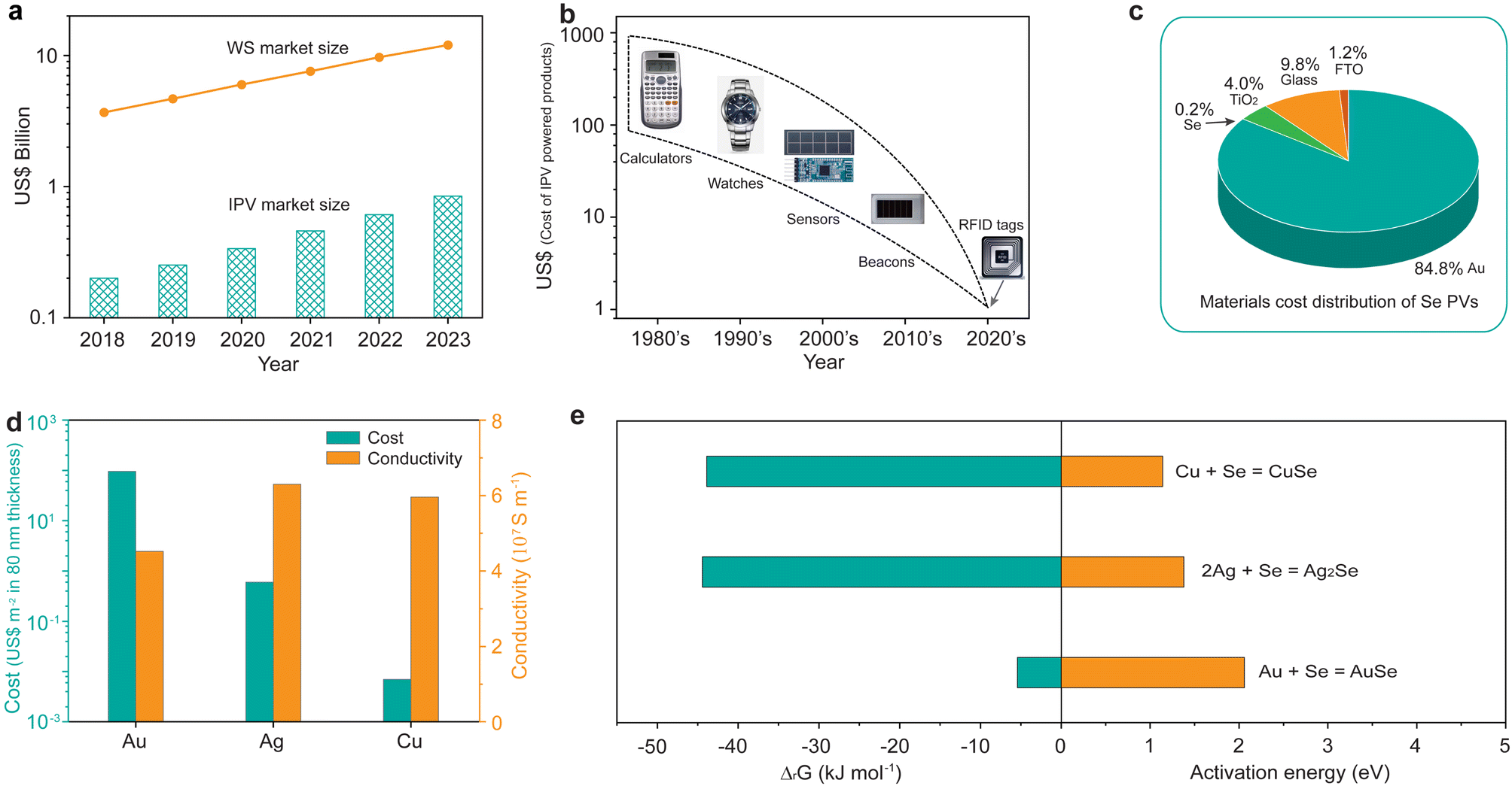 | ||
| Fig. 1 (a) The projected market size of an indoor photovoltaic and wireless sensor, respectively. (b) A summary of the cost of indoor photovoltaic-powered electronic devices. (c) Material cost distribution of widely reported Se PVs. (d) Comparison of the material cost per m2 for 80 nm thickness and the conductivity of Au, Ag, and Cu. (e) Comparison of the Gibbs free energies and activation energies of the reaction between Se and Au, Ag, and Cu. | ||
The early solar-powered electronic devices were usually concentrated on relatively expensive consumer devices such as calculators and watches (Fig. 1b).22,26 The cost of IPVs could be thereby absorbed in those high-price devices. Currently, the IPV-powered devices have been switched to the low-cost IoT devices such as sensors and radio-frequency identification (RFID) tags. This enables the cost of IPVs to be also significantly reduced, matching the low cost of IoT devices. We thereby performed a material cost analysis on the emerging Se IPVs. Fig. 1c shows that the dominant material cost of the widely reported Se PVs is the cost of a Au electrode, accounting for 84.8% of the total material cost. The cost of the absorber material Se only contributes 0.2% to the total cost, which is attributed to the low material cost of Se (Table S1†). The remaining 15% of material costs belong to the cost of TiO2, glass, and fluorine doped tin oxide (FTO). Replacing the high-cost electrode Au with low-cost electrode materials should thereby be quite necessary to reduce the total cost of Se PVs.
In this regard, we chose copper (Cu), another widely used electrode material, to replace the costly Au electrode due to the following two advantages: (i) the cost of a Cu layer with a thickness of 80 nm is as low as 0.007 US$ per m2, which is significantly lower than that of Ag (0.6 US$ per m2) and Au (95.7 US$ per m2);30 (ii) the conductivity of Cu (5.96 × 10⁷ S m−1) is larger than that of Au (4.52 × 10⁷ S m−1), and comparable to that of Ag (6.3 × 10⁷ S m−1), as shown in Fig. 1d. We then calculated the Gibbs free energy of the reaction between Se and Au, Ag, and Cu,31 respectively, and found that all the three electrode materials can react with Se based on the results that all the corresponding ΔG values are negative (Fig. 1e). However, there exist activation energies for the three reactions according to previous reports.32–34 The activation energy for Cu is only 1.14 eV, whereas it is 2.1 eV for Au, about twice that of Cu. The above results suggest that Cu would be easier to react with Se, compared to that of Au, thus explaining the widely-used Au as electrode rather than Cu in Se PVs arising from the easy reaction between Se and Cu.
3.2 Addition of an MoOx isolation layer between Se and Cu layers
We then sought to avoid the reaction between Cu and Se by adding an isolation layer to prevent the direct contact of Se and Cu. We posited that MoOx as a hole-transport layer (HTL) arising from its suitable energy level with t-Se (Fig. S2†) would also serve as an efficient isolation layer due to its relatively high chemical inertness.13,35 Two types of Se thin-film photovoltaic devices were fabricated in a superstrate structure with and without a MoOx isolation layer under the same fabrication conditions. The devices of glass/FTO/TiO2/Se/Cu and glass/FTO/TiO2/Se/MoOx/Cu are labelled as the Se/Cu device and Se/MoOx/Cu device (Fig. 2a and b), respectively. The optimal thickness of the MoOx layer is about 15 nm (Table S2†), which provides a good balance between the high coverage of MoOx on the Se layer and the low conductivity of MoOx. From the optical photographs of two such types of devices (Fig. 2c and d), we see that in contrast to the expected yellow colour of the Se/MoOx/Cu device, the Se/Cu device exhibits a dark blue colour. The different colours of devices with and without a MoOx layer may be attributed to the isolation effect of the MoOx layer.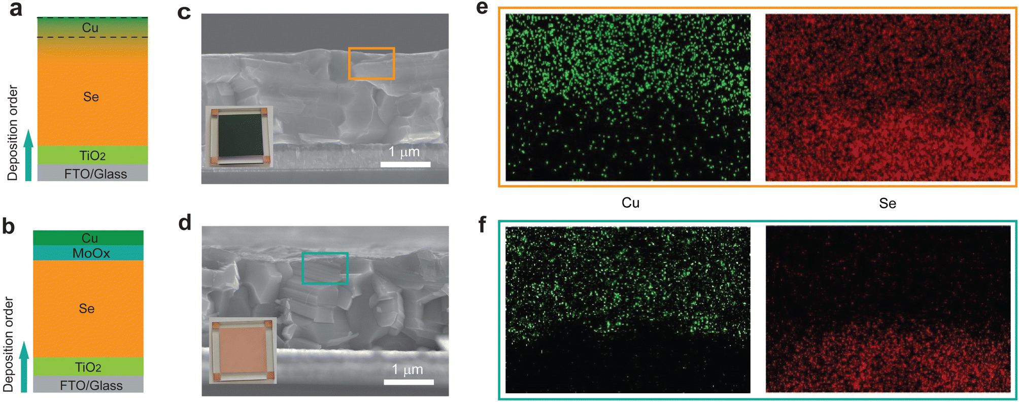 | ||
| Fig. 2 Schematic configurations of (a) glass/FTO/TiO2/Se/Cu and (b) glass/FTO/TiO2/Se/MoOx/Cu devices. Cross-sectional SEM images and top-view photographs of (c) glass/FTO/TiO2/Se/Cu and (d) glass/FTO/TiO2/Se/MoOx/Cu devices. Energy-dispersive spectroscopy elemental mapping of Cu and Se on the surface of (e) glass/FTO/TiO2/Se/Cu and (f) glass/FTO/TiO2/Se/MoOx/Cu devices. | ||
To investigate the Se/Cu interface in these two types of devices, we applied a combination of cross-sectional scanning electron microscopy (SEM) and energy-dispersive X-ray spectroscopy (EDS) elemental mapping to identify the Se and Cu distribution at the Se/Cu interface. For the Se/Cu device, the absence of distinct demarcation and the obvious overlapped edges of Se/Cu in their spatial distribution maps between Se and Cu layers indicate the diffusion of Cu and Se (Fig. 2e). In contrast, the Se/MoOx/Cu device shows sharp edges of Cu and Se (Fig. 2f), illustrating the negligible interfacial diffusion at the Cu/Se interface. The above characterization results thereby suggest that the MoOx layer acts as a diffusion barrier to efficiently prevent the Cu and Se diffusion at the Cu/Se interface.
We next employed X-ray diffraction (XRD) to study the reaction between Se and Cu layers. For the Se/MoOx/Cu device, all diffraction peaks expectedly match well with those of trigonal Se (t-Se) (JCPDS 73-0465) and cubic Cu (JCPDS 04-0836) with no other phase impurities, except the peaks of the FTO substrate (Fig. 3a). This indicates that a 15 nm MoOx isolation layer deposited between Se and Cu layers efficiently prevents the easy reaction between Cu and Se. Furthermore, the XRD pattern of the Se/MoOx/Cu device stored in an ambient atmosphere at room temperature for 1000 h still shows the diffraction peaks of cubic Cu and t-Se with no other emerging diffraction peaks (Fig. S3†), illustrating the durable isolation effect of the MoOx layer. In contrast, for the XDR pattern of the Se/Cu device, the diffraction peak at 43.3° corresponding to the (111) crystal plane of cubic Cu disappears, while two diffraction peaks at 30.4° and 31.0° appear, which are assigned to the (133) and (006) crystal planes of hexagonal CuSe (JCPDS 49-1457). This suggests the reaction between Se and Cu to form CuSe during the thermal evaporation process of Cu atop the Se film. The above results are consistent with the EDS mapping characterization, confirming that the addition of a MoOx layer can efficiently prevent the reaction between Se and Cu.
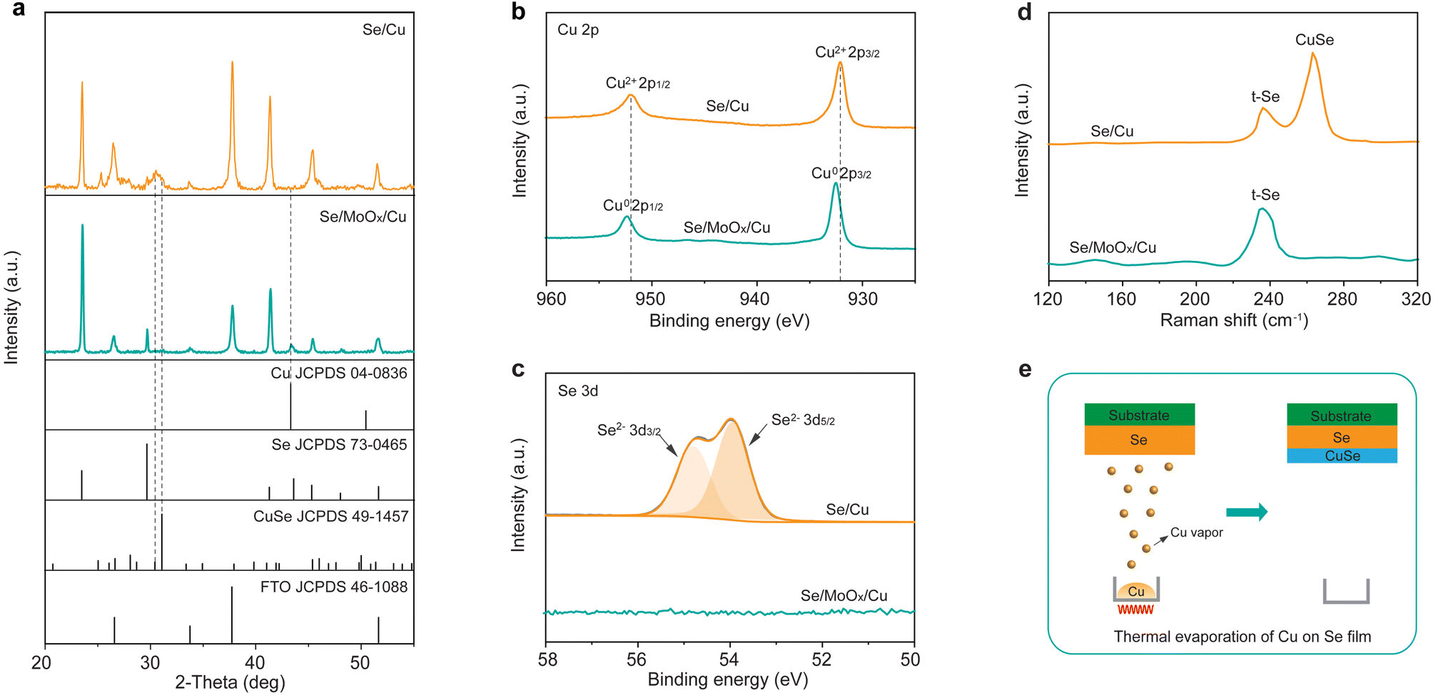 | ||
| Fig. 3 (a) XRD patterns of Se/Cu and Se/MoOx/Cu devices. XPS spectra of (b) Cu 2p and (c) Se 3d in the Se/Cu and Se/MoOx/Cu devices. (d) Raman spectra of Se/Cu and Se/MoOx/Cu devices. (e) Schematic of the reaction between Cu and Se during the thermal evaporation of Cu atop the Se film. | ||
We further applied X-ray photoelectron spectroscopy (XPS) to investigate the element composition and chemical state at the surface of both Se/Cu and Se/MoOx/Cu devices. In the magnified Cu 2p XPS spectrum of the Se/MoOx/Cu device (Fig. 3b), two peaks located at 932.5 and 952.4 eV correspond to the Cu 2p3/2 and 2p1/2 binding energies of elemental Cu0, indicating that the existing state of thermally evaporated Cu atop the Se film is elemental Cu. From the magnified XPS spectrum from 50 to 58 eV (Fig. 3c), we found that Se is not detected in the Se/MoOx/Cu device. Considering the shallow probing depth of XPS (about 10 nm), this thereby indicates that Se doesn't exist at the surface of the Se/MoOx/Cu device. In contrast, we observed that the Cu 2p peaks shift toward a lower binding energy to 932.1 and 952.0 eV when there is no addition of a MoOx layer. This is consistent with the binding energy in CuSe,36 indicating that the thermally evaporated Cu reacts with Se to form CuSe at the surface of the Se/Cu device. No other possible Cu chemical states such as Cu0 and Cu+ are detected in the XPS spectrum of the Se/Cu device considering the perfect Gaussian–Lorentzian peak fitting of Cu 2p. Accordingly, Se exhibits the expected valence of Se2− in CuSe.36 The above XPS results thereby demonstrate the formation of CuSe in the Se/Cu device, and confirm the isolation effect of MoOx, consistent with the XRD results.
Raman spectroscopy was further performed on the Se/Cu and Se/MoOx/Cu devices to evaluate the effect of the MoOx layer. Two Raman peaks located at 236 cm−1 and 263 cm−1 are observed in the spectrum of the Se/Cu device, which are assigned to the vibrational modes of t-Se and hexagonal CuSe,37,38 respectively. This agrees well with the XRD and XPS results. In contrast, there is only one Raman peak at 236 cm−1 assigned to the vibrational modes of t-Se with no signal of CuSe in the spectrum of the Se/MoOx/Cu device. Besides, the Raman spectra of the Se/MoOx/Cu device after long-term storage exhibit the same results, suggesting the durable isolation effect of the MoOx layer to prevent Se and Cu from forming CuSe (Fig. S4†). The above combined material characterization thereby allows us to depict the schematic of the reaction between Se and Cu during the thermal evaporation of Cu atop the Se film; when the Cu vapor reach the Se film, it reacts with Se to form CuSe at the surface of the Se film (Fig. 3e).
3.3 Photovoltaic device performance
We finally measured the current density–voltage (J–V) characteristics of the Se/Cu and Se/MoOx/Cu devices under standard AM1.5G illumination at an intensity of 100 mW cm−2. Fig. 4a shows the J–V curves of the best-performing devices of each type. Compared to the Se/Cu device with a PCE of 3.2% (Voc = 0.65 V, Jsc = 10.1 mA cm−2, FF = 48.4%), the champion Se/MoOx/Cu device exhibits a much higher PCE of 5.4%, with a corresponding Voc of 0.89 V, Jsc of 11.4 mA cm−2, and FF of 53.6%. This low PCE of the Se/Cu device is attributed to the absence of a metal electrode, where the formed CuSe is a typical semiconductor with a bandgap of 1.66 eV.38 This leads to reduced carrier collection and increased carrier recombination, finally resulting in a severe reduction in Voc, Jsc, and FF. We then measured the light intensity-dependent Voc of Se/MoOx/Cu and Se/Cu devices to investigate the recombination. In the equation Voc= (nkBT/q)lnP, n, kB, T, and q are the ideality factor, Boltzmann constant, temperature and elementary charge. Fig. S5† shows that the values of n decrease from 1.8 for Se/Cu devices to 1.5 for Se/MoOx/Cu devices, indicating that trap-assisted recombination is effectively suppressed due to the addition of a MoOx isolation layer. Notably, the performance of Se/MoOx/Cu devices is comparable to that of the conventional well-performing Se/Au devices with a PCE of 5.6% (Voc = 0.89 V, Jsc = 11.5 mA cm−2, FF = 55.0%) (Fig. S6†). Compared to the slightly improved performance from Se/Au devices to Se/MoOx/Au devices, the significantly enhanced performance from Se/Cu devices to Se/MoOx/Cu devices is mainly attributed to the isolation effect of the MoOx layer (Table S3†). The cost of the Se/MoOx/Cu device is only about one-tenth that of the Se/Au device arising from the high-cost Au electrode, dramatically reducing the material cost of Se photovoltaic cells.
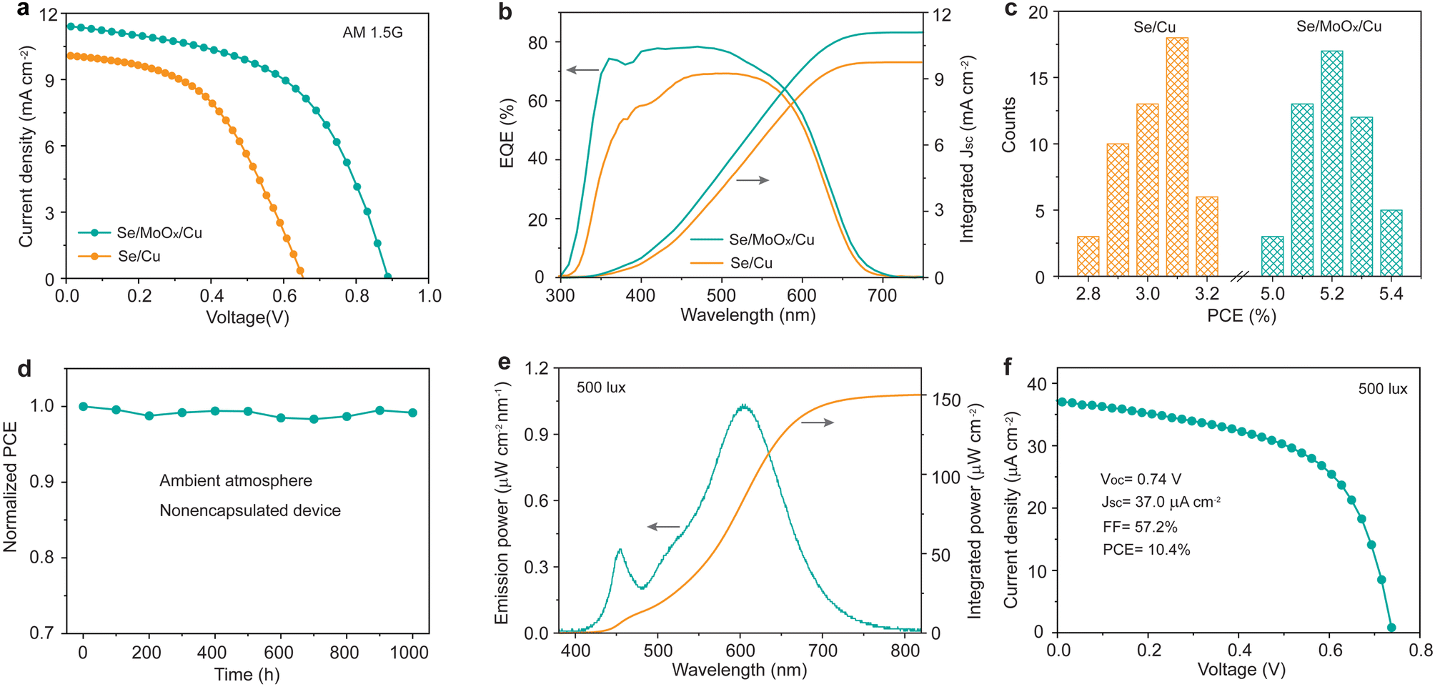 | ||
| Fig. 4 (a) J–V curves of Se/Cu and Se/MoOx/Cu devices under 100 mW cm−2 simulated AM1.5G irradiation. (b) EQE spectra of Se/Cu and Se/MoOx/Cu devices. (c) Histograms of PCE values for 50 Se/Cu and Se/MoOx/Cu devices, respectively. (d) Evolution of normalized PCEs of Se/Cu and Se/MoOx/Cu devices stored in the ambient atmosphere at room temperature and a relative humidity of 50% to 80%. (e) Emission power and integrated power spectra of a 2700 K LED at 500 lux. (f) J–V curve of the Se/MoOx/Cu device under indoor illumination at 500 lux. | ||
External quantum efficiency (EQE) measurement was subsequently performed on such devices (Fig. 4b). The integrated current densities calculated from EQE spectra match well with the Jsc values measured from J–V characterization (within 5% deviation). Particularly, the Se/MoOx/Cu device exhibits an obviously higher EQE in the 300–500 nm wavelength region compared to that of the Se/Cu device, indicating that the Se/MoOx/Cu device possesses lower recombination loss of photogenerated carriers. Fig. 4c shows the statistical photovoltaic performance of 50 devices of both types. The efficiency histograms demonstrate the good repeatability and reliability of the performance improvement by the addition of a MoOx layer between Se and Cu films. The long-term stability test of the unencapsulated Se/MoOx/Cu device was further performed in an air environment at room temperature with a relative humidity of 50% to 80%. It is shown that there is negligible PCE loss of the device after 1000 h of storage (Fig. 4d). The high stability of Se devices thereby demonstrates the long-term stability and durable isolation effect of the MoOx layer, in good agreement with the XRD results.
Considering the suitable wide bandgap of Se for indoor light harvesting, we then measured the IPV performance of the Se/MoOx/Cu device under indoor illumination at 500 lux using a common warm white 2700 K LED as the light source, where the 500 lux illumination is the most frequent value in most indoor environments such as offices, classrooms, libraries, and shopping malls, based on the CIE/ISO standard for lighting design of buildings (CIE S 008/E-2001).20 The corresponding input light intensity of the LED at 500 lux was measured to be 150.1 μW cm−2 (Fig. 4e). All IPV performance measurements were carried out in a homemade testing box with black internal components to prevent the interference of stray light, according to a reliable measurement method for IPVs reported by the Hou group.20,23 The Se/MoOx/Cu device displays a PCE of 10.4% with a corresponding Voc of 0.74 V, Jsc of 37.0 μA cm−2, and FF of 57.2% under indoor illumination at 500 lux (Fig. 4f), comparable to that of the Se/Au devices (Fig. S7†). The integrated current density of the device closely matches the Jsc value measured by J–V characterization under 500 lux indoor illumination (Fig. S8†). The IPV performance of such Se devices is higher than that of commercialized amorphous silicon cells with an indoor PCE below 10% (Table S4†), which is the current IPV industry standard.22 The advantage of low cost combined with a high IPV performance thereby guarantees the future commercialization of Se IPVs for powering IoT wireless sensors.
4. Conclusion
In summary, we substitute low-cost Cu material for the widely used Au electrode in conventional high-performance Se photovoltaic devices, significantly reducing the cost of Se devices by about one order of magnitude. We further introduce an isolation layer of MoOx between Se and Cu films, preventing the direct contact of Se and Cu and avoiding the reaction between Cu and Se; the CuSe formed during the thermal evaporation of Cu dramatically lowers the device performance. The MoOx isolated Cu electrode-based Se devices exhibit a PCE of 10.4% under indoor illumination at 500 lux. This performance is comparable to that of Au electrode-based Se devices, outperforming the present IPV industry standard of amorphous silicon cells with an indoor photovoltaic efficiency below 10%. The unencapsulated devices also show no efficiency loss when stored in the ambient atmosphere for 1000 h, demonstrating the excellent stability of such Se photovoltaic devices. This work thereby provides a cost-effective fabrication of high-performance and stable Se devices, accelerating the commercialization of Se IPVs.Author contributions
Zhouqing Wei: conceptualization, methodology, data curation, and writing – original draft; Wenbo Lu: data curation and investigation; Zongbao Li: data curation and investigation; Mingjie Feng: investigation; Bin Yan: investigation; Jin-Song Hu: writing – review & editing; Ding-Jiang Xue: conceptualization, writing – review & editing, supervision, and funding acquisition.Conflicts of interest
There are no conflicts to declare.Acknowledgements
This work was supported by the National Natural Science Foundation of China (22269019 and 22375206) and the Youth Innovation Promotion Association, CAS (Y2021014).References
- W. Smith, Nature, 1873, 7, 303 CrossRef
.
- W. G. Adams and R. E. Day, Proc. R. Soc. London, 1877, 25, 113–117 CrossRef
- C. E. Fritts, Am. J. Sci., 1883, 26, 465–472 CrossRef
- W. Liu, A. A. Said, W. J. Fan and Q. Zhang, ACS Appl. Energy Mater., 2020, 3, 7345–7352 CrossRef CAS
- S. D. Deshmukh, C. K. Miskin, A. A. Pradhan, K. Kisslinger and R. Agrawal, ACS Appl. Energy Mater., 2022, 5, 3275–3281 CrossRef CAS
- T. H. Youngman, R. Nielsen, A. Crovetto, B. Seger, O. Hansen, I. Chorkendorff and P. C. K. Vesborg, Sol. RRL, 2021, 5, 2100111 CrossRef CAS
- D. M. Chapin, C. S. Fuller and G. L. Pearson, J. Appl. Phys., 1954, 25, 676–677 CrossRef CAS
- I. Hadar, X. Hu, Z.-Z. Luo, V. P. Dravid and M. G. Kanatzidis, ACS Energy Lett., 2019, 4, 2137–2143 CrossRef CAS
- I. Hadar, T.-B. Song, W. Ke and M. G. Kanatzidis, Adv. Energy Mater., 2019, 9, 1802766 CrossRef
- W. Liu, F. Yu, W. Fan, W.-s. Li and Q. Zhang, Small, 2021, 17, 2101226 CrossRef CAS PubMed
- L. Fu, J. Zheng, X. Yang, Y. He, C. Chen, K. Li and J. Tang, Faraday Discuss., 2022, 239, 317–327 RSC
- J. Zheng, L. Fu, Y. He, K. Li, Y. Lu, J. Xue, Y. Liu, C. Dong, C. Chen and J. Tang, Front. Optoelectron., 2022, 15, 36 CrossRef PubMed
- T. K. Todorov, S. Singh, D. M. Bishop, O. Gunawan, Y. S. Lee, T. S. Gershon, K. W. Brew, P. D. Antunez and R. Haight, Nat. Commun., 2017, 8, 682 CrossRef PubMed
- R. Nielsen, T. H. Youngman, H. Moustafa, S. Levcenco, H. Hempel, A. Crovetto, T. Olsen, O. Hansen, I. Chorkendorff, T. Unold and P. C. K. Vesborg, J. Mater. Chem. A, 2022, 10, 24199–24207 RSC
- B. Yan, X. Liu, W. Lu, M. Feng, H.-J. Yan, Z. Li, S. Liu, C. Wang, J.-S. Hu and D.-J. Xue, Sci. Adv., 2022, 8, eadc9923 CrossRef CAS PubMed
-
D. M. Bishop, T. Todorov, Y. S. Lee, O. Gunawan and R. Haight, 2017 44th IEEE Photovolt. Spec. Conf., 2017, pp. 1441–1444 Search PubMed
- W. Lu, Z. Li, M. Feng, H.-J. Yan, B. Yan, L. Hu, X. Zhang, S. Liu, J.-S. Hu and D.-J. Xue, Sci. China: Chem., 2022, 65, 2197–2204 CrossRef CAS
- https://www.shmet.com/ .
- C. Tan, M. Amani, C. Zhao, M. Hettick, X. Song, D.-H. Lien, H. Li, M. Yeh, V. R. Shrestha, K. B. Crozier, M. C. Scott and A. Javey, Adv. Mater., 2020, 32, 2001329 CrossRef CAS PubMed
- Y. Cui, L. Hong, T. Zhang, H. Meng, H. Yan, F. Gao and J. Hou, Joule, 2021, 5, 1016–1023 CrossRef
- E. Hittinger and P. Jaramillo, Science, 2019, 364, 326–328 CrossRef CAS PubMed
- I. Mathews, S. N. Kantareddy, T. Buonassisi and I. M. Peters, Joule, 2019, 3, 1415–1426 CrossRef CAS
- Y. Cui, Y. Wang, J. Bergqvist, H. Yao, Y. Xu, B. Gao, C. Yang, S. Zhang, O. Inganäs, F. Gao and J. Hou, Nat. Energy, 2019, 4, 768–775 CrossRef CAS
- R. Haight, W. Haensch and D. Friedman, Science, 2016, 353, 124–125 CrossRef CAS PubMed
- K.-L. Wang, Y.-G. Yang, Y.-H. Lou, M. Li, F. Igbari, J.-J. Cao, J. Chen, W.-F. Yang, C. Dong, L. Li, R.-Z. Tai and Z.-K. Wang, eScience, 2021, 1, 53–59 CrossRef
- B. Li, B. Hou and G. A. J. Amaratunga, InfoMat, 2021, 3, 445–459 CrossRef CAS
- I. Mathews, S. N. R. Kantareddy, S. Sun, M. Layurova, J. Thapa, J.-P. Correa-Baena, R. Bhattacharyya, T. Buonassisi, S. Sarma and I. M. Peters, Adv. Funct. Mater., 2019, 29, 1904072 CrossRef CAS
- C. Zhang, C. Liu, Y. Gao, S. Zhu, F. Chen, B. Huang, Y. Xie, Y. Liu, M. Ma, Z. Wang, S. Wu, R. E. I. Schropp and Y. Mai, Adv. Sci., 2022, 9, 2204138 CrossRef CAS PubMed
- J. Li, H. Li, L. Ma, S. Zhang and J. Hou, Chin. J. Chem., 2023, 41, 424–430 CrossRef CAS
- Z. Li, Y. Zhao, X. Wang, Y. Sun, Z. Zhao, Y. Li, H. Zhou and Q. Chen, Joule, 2018, 2, 1559–1572 CrossRef CAS
-
J. G. A. Speight, Lange's Handbook of Chemistry, McGraw Hill Book Co., New York, 2005 Search PubMed
- A. Rabenau, H. Rau and G. Rosenstein, J. Less-Common Met., 1971, 24, 291–299 CrossRef CAS
- V. B. Rajkumar and S.-w. Chen, Calphad, 2018, 63, 51–60 CrossRef CAS
- J. O. Thompson, M. D. Anderson, T. Ngai, T. Allen and D. C. Johnson, J. Alloys Compd., 2011, 509, 9631–9637 CrossRef CAS
- D.-J. Xue, Y. Hou, S.-C. Liu, M. Wei, B. Chen, Z. Huang, Z. Li, B. Sun, A. H. Proppe, Y. Dong, M. I. Saidaminov, S. O. Kelley, J.-S. Hu and E. H. Sargent, Nat. Commun., 2020, 11, 1514 CrossRef CAS PubMed
- Y. Mao, H. Zou, Q. Wang and C. Huang, Sci. China: Chem., 2016, 59, 903–909 CrossRef CAS
- M. Marple, J. Badger, I. Hung, Z. Gan, K. Kovnir and S. Sen, Angew. Chem., Int. Ed., 2017, 56, 9777–9781 CrossRef CAS PubMed
- C. Xue, D. Papadimitriou, Y. S. Raptis, W. Richter, N. Esser, S. Siebentritt and M. C. Lux-Steiner, J. Appl. Phys., 2004, 96, 1963–1966 CrossRef CAS
Footnote |
| † Electronic supplementary information (ESI) available. See DOI: https://doi.org/10.1039/d3ta04530g |
| This journal is © The Royal Society of Chemistry 2023 |