
 Open Access Article
 This Open Access Article is licensed under a
 Creative Commons Attribution 3.0 Unported Licence
Air-stable bismuth sulfobromide (BiSBr) visible-light absorbers: optoelectronic properties and potential for energy harvesting†
Xiaoyu
Guo
a,
Yi-Teng
Huang
a,
Hugh
Lohan
 ac,
Junzhi
Ye
a,
Yuanbao
Lin
a,
Juhwan
Lim
b,
Nicolas
Gauriot
b,
Szymon J.
Zelewski
b,
Daniel
Darvill
c,
Huimin
Zhu
da,
Akshay
Rao
b,
Iain
McCulloch
a and
Robert L. Z.
Hoye
*a
ac,
Junzhi
Ye
a,
Yuanbao
Lin
a,
Juhwan
Lim
b,
Nicolas
Gauriot
b,
Szymon J.
Zelewski
b,
Daniel
Darvill
c,
Huimin
Zhu
da,
Akshay
Rao
b,
Iain
McCulloch
a and
Robert L. Z.
Hoye
*a
aDepartment of Chemistry, University of Oxford, South Parks Road, Oxford OX1 3QR, UK. E-mail: robert.hoye@chem.ox.ac.uk
bCavendish Laboratory, University of Cambridge, JJ Thomson Ave., Cambridge CB3 0HE, UK
cDepartment of Materials, Imperial College London, Exhibition Road, London SW7 2AZ, UK
dDepartment of Physics, University of Strathclyde, Glasgow G4 0NG, UK
First published on 25th September 2023
Abstract
ns2 compounds have recently attracted considerable interest due to their potential to replicate the defect tolerance of lead-halide perovskites and overcome their toxicity and stability limitations. However, only a handful of compounds beyond the perovskite family have been explored thus far. Herein, we investigate bismuth sulfobromide (BiSBr), which is a quasi-one-dimensional semiconductor, but very little is known about its optoelectronic properties or how it can be processed as thin films. We develop a solution processing route to achieve phase-pure, stoichiometric BiSBr films (ca. 240 nm thick), which we show to be stable in ambient air for over two weeks without encapsulation. The bandgap (1.91 ± 0.06 eV) is ideal for harvesting visible light from common indoor light sources, and we calculate the optical limit in efficiency (i.e., spectroscopic limited maximum efficiency, SLME) to be 43.6% under 1000 lux white light emitting diode illumination. The photoluminescence lifetime is also found to exceed the 1 ns threshold for photovoltaic absorber materials worth further development. Through X-ray photoemission spectroscopy and Kelvin probe measurements, we find the BiSBr films grown to be n-type, with an electron affinity of 4.1 ± 0.1 eV and ionization potential of 6.0 ± 0.1 eV, which are compatible with a wide range of established charge transport layer materials. This work shows BiSBr to hold promise for indoor photovoltaics, as well as other visible-light harvesting applications, such as photoelectrochemical cells, or top-cells for tandem photovoltaics.
Introduction
Discovering semiconductors that are simultaneously efficient, nontoxic, stable and cost-effective has long been the holy grail of the thin film photovoltaics community.1–3 The arrival of lead-halide perovskites (LHPs) onto the scene has not only disrupted the materials focus of the community, but also shifted the emphasis of research from bandgap and absorption coefficient to more strongly encompass charge-carrier transport properties.6,7 This is because the key to the success of LHPs as photovoltaic materials is not only their strong absorption of light over the visible and near-infrared wavelength ranges, but also their long diffusion lengths on the micron scale, which allows efficient charge-carrier collection. Remarkably, these long transport lengths are achieved despite having higher defect densities (1013 to 1017 cm−3 in polycrystalline thin films) than conventional semiconductors, such as silicon (108 cm−3 typical defect densities).8,9 This has prompted groups to explore whether such defect tolerance could be replicated in other classes of materials, especially those which can overcome the toxicity and stability limitations of LHPs. It is proposed that the defect tolerance of LHPs arises in part as a result of its unusual electronic structure at its band-edges, which comes about from the strong contributions of the valence 6s2 electrons from the Pb2+ cation.10,11 Thus, efforts at finding electronic analogs to LHPs have focused on materials containing heavy post-transition metal cations with stable valence s2 electrons (e.g., Sn2+, Sb3+ or Bi3+), and these are termed ‘ns2 compounds’.12 Although the majority of ns2 compounds investigated are perovskites, or have a perovskite-derived structure (e.g., vacancy-ordered triple perovskites), we are in no way limited to perovskite compounds to achieve a qualitatively similar electronic structure at the band-edges as LHPs.11 A handful of non-perovskite materials have therefore been explored, such as BiOI.13,14 Many of the ns2 compounds explored tend to have wider bandgaps than iodide-based LHPs.15 Whilst this limits their performance in solar cells, their bandgaps are ideal for indoor photovoltaics (IPVs), for which the optimal bandgap is 1.9 eV.15IPVs can improve the sustainability of the Internet of Things (IoT), which describes an ecosystem of devices connected together via the cloud, embedding intelligence into infrastructure.16,17 This results in more energy-efficient societies (thereby contributing to a reduction in CO2eq footprint), and is having an impact on a wide range of fields, such as information systems, agriculture and cybersecurity.18–21 Nonetheless, the majority of IoT devices are battery-powered, which presents two major challenges. Firstly, the practicality challenges associated with replacing or recharging primary and secondary batteries is expected to prevent >80% of the potential of the IoT from being realized.22 Secondly, replacing billions of batteries annually presents a substantial sustainability challenge due to the waste created and drain upon the earth's limited availability of elements required for fabricating batteries.15,23 These practicality and sustainability challenges can be addressed by using IPVs to harvest the energy widely available from indoor lighting, which has high energy density, is predictable and places no restrictions on the distance between the energy supply and harvester.15,24 Coupling together the IPV and battery on the IoT node can substantially extend the lifetime of the battery. Given the regular time intervals in which indoor lighting is available, the high energy density of batteries is not required in some applications, such that more sustainable energy storage devices (e.g., supercapacitors) can be used. However, the current industry-standard IPV material (hydrogenated amorphous silicon, a-Si:H) is inefficient (4.4–9.2% power conversion efficiency, PCE).15 Current alternatives with indoor PCEs >30% include dye-sensitized solar cells (DSSCs), organic photovoltaics (OPVs) and LHP PVs. However, these are limited by: (1) the use of toxic solvents in their synthesis (e.g., chloroform or N,N-dimethylformamide); (2) high synthetic complexity, increasing costs (OPV); and (3) the presence of toxic elements (Pb) and poor stability (LHPs).15,25,26 It is therefore critical to develop non-toxic alternative materials that not only can achieve high PCEs, but are also stable and can be processed using simple, cost-effective methods that do not make use of toxic precursors or expensive catalysts. Many inorganic Pb-free ns2 compounds have simple chemistry along with high air stability, and very recently, some of them have been shown to exhibit high spectroscopic limited maximum efficiencies (SLMEs) under indoor lighting.15,27 The ns2 materials realized in IPVs so far include BiOI, Cs3Sb2(I,Cl)9, and Ag–Bi–I semiconductors.27–30 These materials are currently too early in their development for life cycle analyses, but the comparatively low temperatures used in their processing, along with the capability for many of these materials to be processed with low-toxicity solvents, or solvent-free, suggest that the CO2eq footprint and human health toxicity would be similar to or smaller than those of lead-halide perovskites and organic photovoltaics. The highest PCE of up to 10% has been reported in Cu2Ag(Bi,Sb)I6 materials under indoor lighting.31 Whilst further optimization is necessary for these materials, it is essential at this early stage to search more broadly for promising ns2 compounds that fit in the field of IPV.
Among these ns2 compounds, BiSI has received attention as a potential solar absorber, especially because of its strong light absorption.32–35 However, the experimental indirect bandgap is 1.57 eV,34 falling below the optimal value (1.9 eV) for indoor light harvesting. This bandgap can be widened to 1.9–2.0 eV by substituting I for Br.36 However, there have been very few reports of BiSBr. The current literature shows the use of BiSBr to harvest light from a filtered Xe lamp to produce a measurable photocurrent in photoelectrochemical systems.36 Computations also show that the upper valence band is comprised of bonding and antibonding orbitals between Bi 6s and the two anion p orbitals, while the lower conduction band is comprised of the overlap between Bi 6p and anion p orbitals.37 This electronic band structure is similar to that present in LHPs,6 but the contribution from Bi 6s to the upper valence band in BiSBr is smaller than Pb 6s in LHPs, such that the valence band maximum (VBM) is flatter in BiSBr. Nevertheless, the conduction band remains disperse, leading to a small average electron effective mass of 0.52m0 (m0 is the rest mass of electrons), which is much smaller than the hole effective mass (3.73m0).37 Additionally, BiSBr also exhibits large spin–orbit coupling, due to the presence of the heavy, polarizable Bi3+ cation. As a consequence of this, BiSBr is predicted to have a high ionic dielectric constant of ∼30 (compared to an ionic dielectric constant of 20 for MAPbI3),6,37 which could contribute to Coulombically screening out charged defect states from charge-carriers, thus reducing the non-radiative recombination rate. Furthermore, BiSBr has a quasi-one-dimensional crystal structure, with inorganic chains held together by weak van der Waals interactions (Fig. 1a). Such a structure may enable the surfaces or interfaces to avoid being terminated with dangling bonds, and thereby minimize surface recombination.38 Surprisingly, very little is known about the charge-carrier kinetics of BiSBr thus far, and this material has not been investigated for indoor light harvesting. Furthermore, despite the great efforts on BiSBr single crystals, nanocrystals, and powders,36,39 BiSBr is still rarely fabricated as thin films, which limits its ultimate application in photovoltaics.
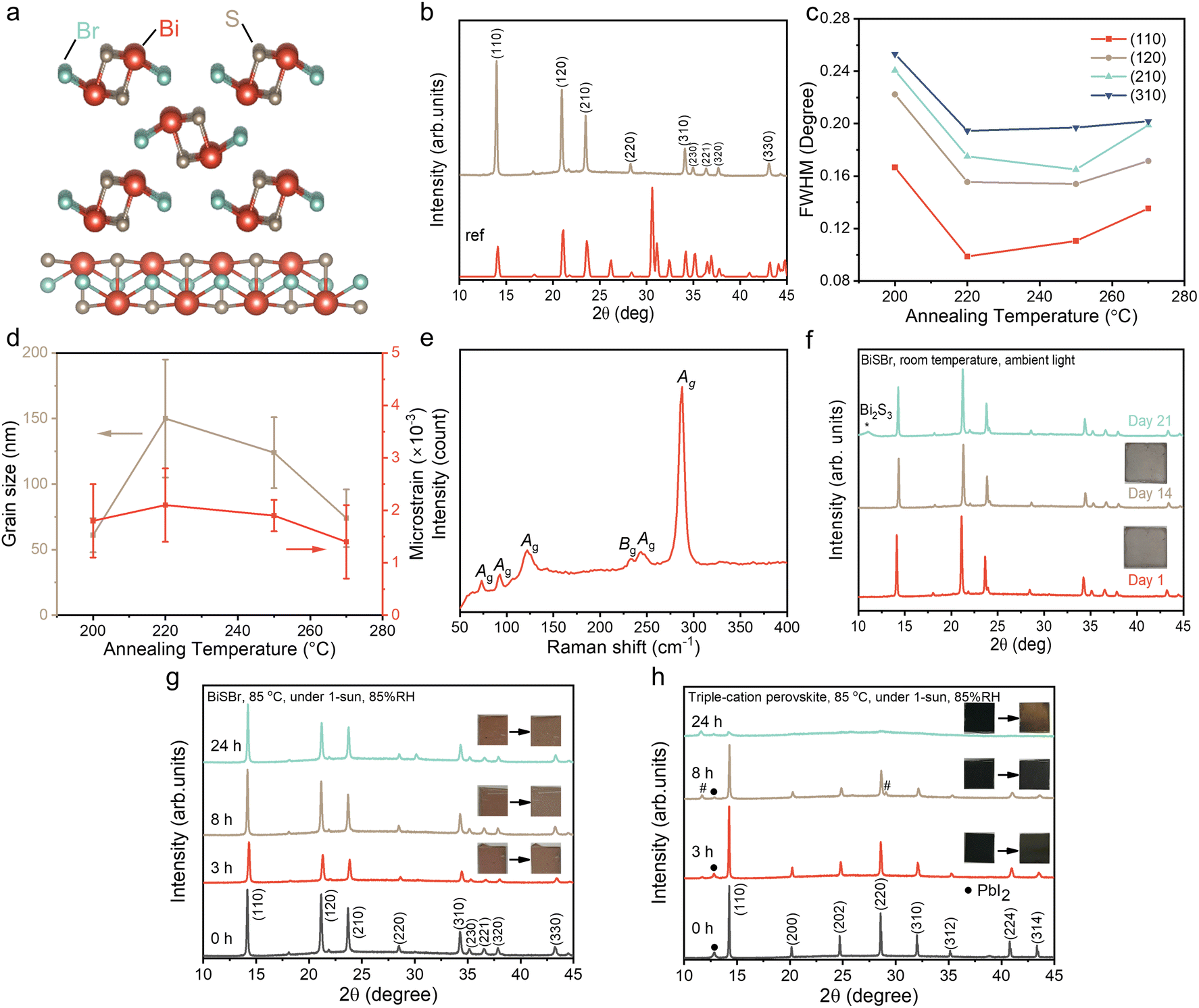 | ||
| Fig. 1 (a) Crystal structure of BiSBr viewed along the c-axis (top) and b-axis (bottom). (b) X-ray diffraction (XRD) pattern of BiSBr thin film annealed at 250 °C for 10 min. The Miller indices are labelled, and the measured diffraction pattern is compared to the reference pattern (ICSD Coll. Code: 31389). (c) Full width at half maximum (FWHM) of the main diffraction peaks from BiSBr annealed at different temperatures for 10 min. (d) Evolution of the average grain size and microstrain in BiSBr thin films for different annealing temperatures, as determined using Williamson–Hall analysis. (e) Raman spectra of BiSBr thin film annealed at 250 °C for 10 min. Evolution of XRD patterns and visual appearance of (f) BiSBr films stored in ambient air under standard laboratory-bench conditions (50–60% relative humidity, as well as (g) BiSBr and (h) triple-cation perovskite (Cs0.05(MA0.17FA0.83)0.95Pb(I0.83Br0.17)3) thin films under 1-sun illumination, at 85 °C and 85% relative humidity over 24 h. # means delta-phase peak for perovskite. | ||
In this work, we developed a solution processing route to realize phase-pure and stoichiometric BiSBr thin films, as verified using X-ray diffraction (XRD), Raman spectroscopy and energy dispersive X-ray spectrometry (EDX) measurements. The environmental stability was evaluated by tracking the evolution of its XRD pattern and visual appearance over time when stored in ambient air without encapsulation, as well as over a 24 h period under 1-sun illumination, at 85 °C and 85% relative humidity. The optoelectronic properties were determined through absorption coefficient (using a combination of UV-visible spectrophotometry and photothermal deflection spectroscopy) and photoluminescence (PL) measurements. We also calculated the spectroscopic limited maximum efficiency (SLME) of BiSBr under indoor lighting based on its absorption coefficient spectrum and nature of its bandgap. The charge-carrier kinetics were evaluated by measuring the PL lifetime. Finally, in order to evaluate the compatibility of BiSBr with other transport layers, its band positions were determined through photoemission spectroscopy and Kelvin probe measurements.
Experimental
BiSBr thin film synthesis
The solution preparation and spin coating processes were both conducted in a N2-filled glove box (O2 < 0.1 ppm, H2O < 5 ppm). 0.596 g bismuth(III) bromide (BiBr3, ≥98%, Sigma Aldrich), and 0.303 g thiourea (ACS reagent, ≥99%, Sigma Aldrich) were dissolved into 1 ml dimethyl sulfoxide (DMSO, anhydrous, ≥99.9%, Sigma Aldrich) to form a 45 wt% solution. All of the chemicals were used as received. The solution was stirred for 3 h at room temperature before being filtered through 0.45 μm PTFE membrane (Fisher Scientific). The substrates (glass or quartz) were cleaned by ultrasonication in soapy water, acetone and ethanol successively for 15 min each. After 20 min of UV-ozone cleaning (UV Ozone Cleaner UVC-1014), the substrates were taken into a N2 glovebox for thin film deposition. To deposit the films, a 1 cm2 substrate was placed onto a vacuum-sealed chuck, and the 30 μl solution was spread onto the substrate before it was spun at 4000 rpm for 30 s. The substrates were then stored overnight in an evacuated antechamber before being annealed at 250 °C for 10 minutes.Measurement and characterization
X-ray diffraction (XRD) measurements were performed on BiSBr thin films deposited onto glass substrates. The measurements were taken in air at room temperature using a Bruker D8 Advance Eco instrument with Cu Kα radiation. PESA (photoelectron spectroscopy in air) spectra were recorded in air using a KP Technology APS02 system with excitation wavelengths of ca. 180–280 nm. Raman spectra were acquired from a commercial Raman microscope setup (Renishaw inVia). Before use, the system was auto calibrated from the software using a c-Si calibration standard to its reference Raman shift peak at 520 cm−1. The samples were excited with a 532 nm wavelength continuous wave (cw) laser source (torus mpc3000, 750 mW) using a 20× objective lens at 5% laser intensity, acquisition time 5 s. A grating of 1800 lines mm−1 was used throughout the measurements. The PL spectrum was also acquired using the same system and conditions. The accelerated environmental stability test was performed using a BBZM-III solar simulator (Bobei Lighting Electrical Appliance Factory), calibrated to 1 sun illumination (AM1.5G) with a KG-5 silicon reference cell certified by Newport. Simultaneously, the thin films were mounted on a hotplate at 85 °C, and a small cup of water was placed next to the thin films to increase the relative humidity to 85%, which was measured by a humidity meter (S. Brannan & Sons Ltd). For photothermal deflection spectroscopy (PDS) measurements, BiSBr films were spin-coated on Spectrosil® 2000 quartz substrates and immersed in an inert liquid with a high thermo-optic coefficient, FC-72 Fluorinert (3M Company). The sample surface was illuminated perpendicularly with a monochromatic beam from a 250 W halogen lamp (Newport) integrated with a 250 mm focal length monochromator (CVI DK240) and modulated with a mechanical chopper at 10 Hz. Nonradiative recombination processes at the film's surface would result in a temperature gradient and, consequently, a refractive index gradient in the surrounding liquid. A 670 nm CW diode laser beam was deflected by the liquid's refractive index and detected by a quadrant photodiode, with the signal amplitude demodulated by a lock-in amplifier (Stanford Research Systems SR830). XPS spectra was acquired using a Thermo Scientific XPS with a monochromated Al Kα X-ray (1486.7 eV) source. Photoluminescence (PL) imaging and PL lifetime measurements were performed using a home-built optical microscope. A 520 nm wavelength excitation was provided by inserting a 520 nm bandpass filter (Thorlabs) into a pulsed supercontinuum white light (Fianium Whitelase) source with a repetition rate of 5 MHz. The optical image was obtained under wide-field excitation and then the laser beam was focused onto the samples using a 100× air objective lens with a numerical aperture of 1.25 for PL lifetime measurement. Then the collected beam was sent to either the EMCCD camera for optical imaging (Photometrics QuantEM 512SC) or Single Photon Avalanche Photodiode for TCSPC lifetime measurement through a 660 nm band pass filter. Secondary electron microscopy (SEM) images of as deposited films were acquired with the Zeiss-Merlin FEG-SEM/EDS platform using an accelerating voltage of 10 keV and a probe current of 250 pA. Energy dispersive X-ray spectrometry (EDX) mapping was carried out in the same SEM chamber using an accelerating voltage of 13 keV and an Oxford Instruments X-max 150 detector.Computations
Ab initio electronic structure calculations were carried out under the Kohn–Sham formulation of density functional theory (DFT)40 using the regularized and restored SCAN (r2SCAN) meta-generalized gradient approximation (mGGA) functional of Furness et al.41 as implemented in the Vienna ab-initio Simulation Package (VASP)42–44 using the projector augmented wave (PAW) method.45 Forces were found to converge to an average difference of <0.4 meV Å−1 on a 3 × 4 × 7 Γ-centered grid using a plane wave cut-off of 400 eV and a self-consistent field (SCF) loop tolerance (EDIFF) of 10−7 eV. Convergence runs were set up and analyzed using vaspup 2.0.46 The crystal structure was optimized from an experimental starting point (ICSD Coll. Code 31389) using the conjugate gradient algorithm of Press et al.47 and a tolerance of 5 × 10⁻⁴ meV Å−1. The density of states (DOS) converged on a denser 7 × 6 × 15 k-point grid using the tetrahedron method with Blöchl corrections.48 Band structures were calculated using the zero-weighted method and a sampling density of 60 k-points/segment. Band structure plots and KPOINTS files were generated using sumo.49Results and discussion
Thin film synthesis and air-stability of BiSBr
Inspired by BiSI and chalcogenides, we proposed two possible solution processing routes for BiSBr thin films: (1) using a thiol-amine alkahest solvent,50 and (2) the use of thiourea as the sulfur source dissolved in a polar aprotic solvent, mixed with the metal-halide salt.51 For the first route, we dissolved Bi2S3 and BiBr3 in 1![[thin space (1/6-em)]](https://www.rsc.org/images/entities/char_2009.gif) :10 v/v ethane-1,2-dithiol and ethylenediamine. However, it was found that the chalcohalide phase could not be achieved here. Instead, we obtained a mixed phase of the halide and chalcogenide precursors, which was partly due to the low solubility of Bi2S3. For the second route, we found BiBr3 and thiourea precursors to be readily dissolved in dimethyl sulfoxide (DMSO), which is a polar aprotic solvent at room temperature. As will be explained in detail below, this process led to phase-pure chalcohalide thin films. Unlike Pb, the precursors used for BiSBr are fully compliant with the EU Restriction of Hazardous Substances directive (RoHS), and are not known to be bioaccumulative. The DMSO solvent is substantially safer than the N,N-dimethylformamide (DMF) or chloroform solvents commonly used for LHP solar cells, OPVs, or DSSCs (note, however, that standard personal protective equipment should still be used when handling DMSO). The process we developed here also avoids the use of expensive catalysts. Given these factors, and the low synthetic complexity of BiSBr, there is potential for this material to be manufactured cost-effectively and sustainably in the future.
:10 v/v ethane-1,2-dithiol and ethylenediamine. However, it was found that the chalcohalide phase could not be achieved here. Instead, we obtained a mixed phase of the halide and chalcogenide precursors, which was partly due to the low solubility of Bi2S3. For the second route, we found BiBr3 and thiourea precursors to be readily dissolved in dimethyl sulfoxide (DMSO), which is a polar aprotic solvent at room temperature. As will be explained in detail below, this process led to phase-pure chalcohalide thin films. Unlike Pb, the precursors used for BiSBr are fully compliant with the EU Restriction of Hazardous Substances directive (RoHS), and are not known to be bioaccumulative. The DMSO solvent is substantially safer than the N,N-dimethylformamide (DMF) or chloroform solvents commonly used for LHP solar cells, OPVs, or DSSCs (note, however, that standard personal protective equipment should still be used when handling DMSO). The process we developed here also avoids the use of expensive catalysts. Given these factors, and the low synthetic complexity of BiSBr, there is potential for this material to be manufactured cost-effectively and sustainably in the future.
The as-deposited films were crystallized over a range of annealing temperatures (from 200 to 270 °C) for 10 min and 30 min, and the effect on bulk stoichiometry, crystallinity and phase-purity were measured through EDX (Table S1, ESI†) and XRD (Fig. 1b). We found that films annealed at low temperatures were Br-rich, and became closer to the ideal stoichiometry when the annealing temperature was increased to 250 °C (Table S1, ESI†). When annealed at this temperature for 10 min inside a N2-filled glovebox, the Bi:S:Br ratio reached was 1.00:1.01:1.12. Annealing for longer than 10 min or at higher temperatures led to the films becoming non-stoichiometric again, which is due to the formation of phase impurities such as BiBr3, as verified from the XRD patterns of 270 °C-annealed (10 min) sample (Fig. S1, ESI†).
The diffraction pattern of the optimized BiSBr film annealed at 250 °C for 10 min is shown in Fig. 1b, which closely matches with the reference pattern (ICSD database, Coll. Code: 31389). The texture coefficients were calculated (Table S2, ESI†). Although the values of the texture coefficient change with annealing conditions, the preferred orientation consistently remained (110). The preferred orientation may be altered by choosing different substrates for BiSBr deposition and controlling the deposition parameters in the future.52 We used Pawley fitting53 to examine the structure of these thin film materials in more detail. The overall Rwp was 4.4%, showing there to be a close fit, with no major peaks unaccounted for by the BiSBr reference pattern (see Fig. S2, ESI†). This result indicates the films obtained here to be phase pure within the detection limits of the measurement. The broad background spanning from 17 to 30° 2θ originates from the amorphous glass substrate these films were deposited onto.6
The structure of BiSBr viewed from the c-axis and b-axis is depicted in Fig. 1a. This shows the quasi-one-dimensional nature of BiSBr (centrosymmetric orthorhombic space group, Pnma), with parallel double chains of [(BiSBr)∞]2 held together by strong Bi–S and Bi–Br polar covalent bonds. In the constituents of these double chains, a Bi atom is connected in a zigzag configuration to three S and two Br atoms that are separated from the other parallel chain. Each of these double chains are linked together by weak van der Waals interactions. From the quasi-one-dimensional crystal structure of BiSBr, one may assume that the (110) preferred orientation we obtained in these thin films is sub-optimal for photovoltaic devices with a conventional vertical architecture.52 However, investigations into the related 1D ns2 semiconductors, Sb2S3 and Sb2Se3, found that the electronic dimensionality between ribbons was higher than 1D, such that there was still efficient charge-carrier transport.54 Furthermore, a challenge with 1D semiconductors having (hk1) preferred orientation is that this can lead to a discontinuous nanorod morphology, resulting in shunting.55,56 Further work is needed to understand the electronic dimensionality of BiSBr, and approaches to tune its preferred orientation in thin films.
To understand the effects of the annealing conditions on the structure of the BiSBr films, we analyzed the line broadening of the diffraction patterns. The full width at half maximum (FWHM) of the main diffraction peaks (Fig. 1c) were obtained from profile fitting on the XRD patterns. As the annealing temperature increased from 200 to 220 °C, there was an evident overall reduction in FWHM, which can arise from an increase in grain size or a decrease in strain in the films. Subsequently, with further increases in the annealing temperature up to 270 °C, the FWHM became more stable across the different annealing temperatures. To understand these observations in more detail, we performed Williamson–Hall analysis on the FWHM to extract the crystallite size and microstrain for each sample (Fig. S3, ESI†); note that instrument broadening was accounted for, as detailed in the ESI. The grain size was obtained from the vertical intercept of the Williamson–Hall plot, while the microstrain was obtained from the slope, and the uncertainties were extracted from fitting (Table S3, ESI†). This analysis, shown in Fig. 1d, reveals no significant differences in crystallite size and microstrain above uncertainty among the various annealing temperatures, with the exception of an increase in grain size as the annealing temperature increased from 200 to 220 °C. Overall, these data show that the films were well crystallized with low microstrain, with the films annealed at 250 °C for 10 min giving the highest phase purity. We therefore used these films for all subsequent characterization.
The phase-purity of this film was further verified through Raman scattering measurements. The point group of BiSBr is D2h16, which contains nine Raman active modes. These are: six Ag modes (287, 250, 121, 92, 75, 41 cm−1) and three modes with B1g, B2g or B3g symmetry (for convenience we refer to these are Bg-type modes). In ref. 57, only Bg-type modes at 234 and 46 cm−1 were detected. Interestingly, as shown in Fig. 1e, five Ag modes (at 288, 243, 122, 93, 73 cm−1), along with one Bg-type mode (234 cm−1) were measured in our BiSBr films. The low energy peaks at 41 (Ag) and 46 cm−1 (Bg-type) could not be measured because of instrument limitations. There were no distinct peaks that were not accounted for, consistent with the film being phase pure. We also note that the dominant Raman peak is the Ag peak at 287 cm−1, which is associated with a symmetric breathing mode, and this would dominate Fröhlich coupling in BiSBr.
Finally, we evaluated the environmental stability of BiSBr. This was achieved through the standard approach of storing thin films without encapsulation in ambient air. Over the course of 21 days, the temperature of the laboratory was 23 ± 2 °C, whilst the relative humidity varied between 50–60%. The visual appearance and diffraction pattern of the BiSBr film remained unchanged (Fig. 1f) after 14 days. As we extended the duration of the stability test to 21 days, we observed the appearance of a small Bi2S3 phase impurity peak (Fig. 1f). For comparison, methylammonium lead iodide perovskite would degrade within only 5 days under similar conditions,58 showing BiSBr to exhibit higher air stability.
Additionally, the environmental and photo-stability of unencapsulated BiSBr thin films under 1-sun illumination, and storage at 85 °C and 85% relative humidity, was investigated with comparison to a state-of-the-art triple-cation perovskite thin film reference (Fig. 1g and h). The BiSBr thin film was synthesized by annealing at 250 °C for 10 min, and the perovskite thin film was fabricated according to our previous publication.59 Afterwards, six thin film samples (three for each material) were mounted on a hotplate at 85 °C, and a large transparent beaker cover was placed on top, with a small cup of water placed next to the thin films to increase the humidity (detected by humidity meter) of the surrounding environment. Simultaneously, the thin films were illuminated under 1-sun. We took out two of the samples (one BiSBr and one perovskite) after 3, 8 and 24 h, respectively, and then took photographs and measured the XRD pattern. The visual appearance and diffraction pattern of the BiSBr films remained unchanged after 24 h of exposure to these conditions. In contrast, degradation products (delta phase, as well as more PbI2) appeared as impurities in the lead-halide perovskite film after 8 h of testing, along with a color change from black to slightly reddish. At the end of the 24 h test, almost no perovskite peaks could be detected from XRD measurements, and the film appeared yellow. Thus, BiSBr is significantly more environmentally and photo-stable than triple-cation perovskite thin films.
Optoelectronic properties and optical limit in efficiency
We determined the absorption coefficient of BiSBr through UV-visible spectrophotometry (UV-vis) and PDS. From UV-vis, we can determine the absolute absorption coefficient of BiSBr by measuring transmittance and reflectance, along with measuring the thickness of the films (Fig. S4, ESI†). However, this technique is not very accurate in the below-bandgap region because of substrate effects (namely substrate absorption and optical interference), which become dominant as the absorption coefficient decreases by orders of magnitude. We therefore used PDS to determine the sub-bandgap absorbance more accurately (Fig. S5, ESI†); see details of this technique in ref. 60. The Urbach energy estimated from these PDS measurements is 115 ± 4 meV (please see Fig. S6, ESI† for details). However, PDS cannot measure the absolute absorption coefficient, and saturates in the highly-absorptive region. We therefore used UV-vis-determined values of the absorption coefficient from 2.1 to 2.8 eV, and scaled the relative absorbance from PDS to match with the absorption coefficient from UV-vis at 2.1 eV to obtain the overall absorption coefficient profile shown in Fig. 2a. This profile demonstrates a gradual increase in absorption coefficient for photon energies >1.6 eV, followed by a sharp increase to >104 cm−1 at >2.1 eV.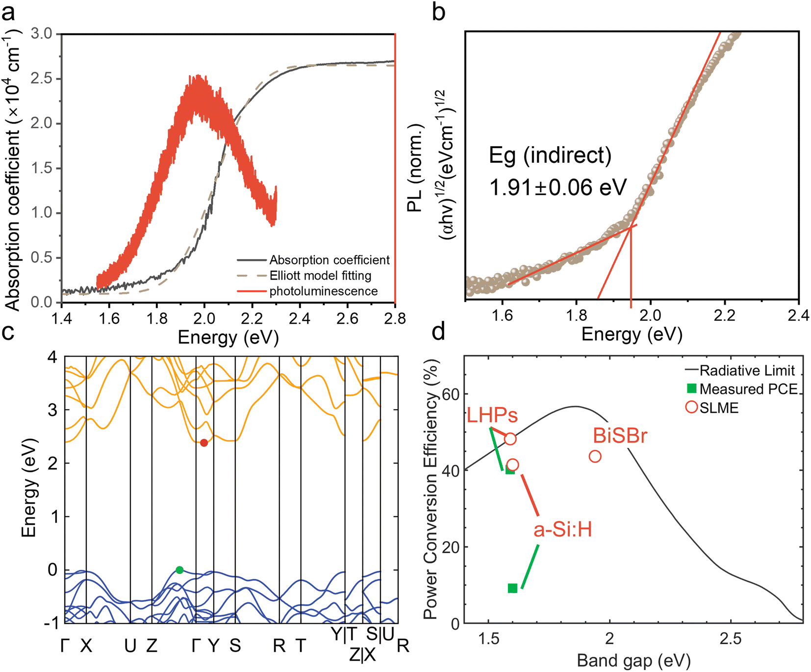 | ||
| Fig. 2 (a) Absorption coefficient and photoluminescence (PL) spectra of BiSBr film on a quartz substrate, as well as Elliott model fitting of the absorption coefficient spectrum. The absorption coefficient spectrum was obtained from UV-vis (transmittance and reflectance) measurements (2.1–2.8 eV) and photothermal deflection spectroscopy (PDS) measurements (1.4–2.1 eV). (b) Tauc plot from PDS measurements to estimate the indirect bandgap. (c) Band structure of BiSBr calculated using r2SCAN functional. (d) Spectroscopic Limited Maximum Efficiency (SLME) of various materials in comparison to the radiative limit (RL) and maximum power conversion efficiency experimentally reported. LHP is lead-halide perovskite. | ||
From Elliott model fitting,61 the exciton binding energy of BiSBr was found to be 20 meV, which is below the thermal energy at room temperature. This result is also consistent with the absence of excitonic peaks in the absorption spectrum (Fig. 2a). We would therefore expect free charge-carriers to dominate the photogenerated species present in BiSBr.
Promisingly, we observed photoluminescence (PL) from BiSBr films (Fig. 2a) at room temperature. This PL peak is centered at 1.9 eV, matching the optical bandgap of this material. The absence of a red shift in PL is consistent with the small exciton binding energy in this material.
To derive numerical values of the bandgap, we constructed Tauc plots using the PDS data rather than UV-vis data because PDS measurements provided a more accurate measure of the absorption onset, with reduced sub-bandgap absorption. As shown in Fig. 2b & S7, ESI,† the first direct transition of the BiSBr thin film is 2.03 ± 0.01 eV, and the first indirect transition is 1.91 ± 0.06 eV. This confirms that the bandgap of BiSBr is indirect, which agrees with the computed band structure of this material (Fig. 2c). From this computed E vs. k diagram, BiSBr has a valence band maximum (VBM) between the Γ and Z points, and conduction band minimum (CBM) between the Γ and Y points. The computed band structure shown in Fig. 2c was determined using the Kohn–Sham formulation of density functional theory (DFT) and r2SCAN functional. Due to the well-known bandgap problem of DFT, we cannot expect absolute bandgaps to correlate well with experiment at this level of theory, however the indirect nature of the band edge is correctly predicted. We calculated the difference between the first direct transition and indirect bandgap to be 0.06 eV, which is within error of the experimentally determined value (0.12 ± 0.06 eV). Dispersion-corrected van der Waals functionals were also tested, however the inclusion of long-range interactions did not affect the nature of the band edges, as shown in Fig. S8 and Table S4, ESI.† The closeness in energy between the indirect bandgap and first direct transition is consistent with the PL peak being coincident with the optical bandgap (Fig. 2a).
To evaluate the potential of BiSBr for indoor photovoltaics, we calculated the spectroscopic limited maximum efficiency (SLME) under a standard 1000 lux white light emitting diode (WLED) spectrum. The SLME model estimates the maximum efficiency that a light-harvesting material can potentially reach if all absorbed photons can be converted into free charge-carriers that can all be extracted.62 The level of non-radiative recombination is estimated based on the difference in energy between the bandgap and the first direct transition, which we took to be 0.1 eV for this calculation. This method is an improvement over calculating the Shockley–Queisser limit for an indoor light spectrum because the experimentally-determined optical absorption spectrum of the material is accounted for, and it is not assumed that all recombination processes are radiative. The detailed methodology for calculating SLME is given in our previous work,27 and from this we determined the SLME (under WLED illumination) of BiSBr to be 43.6% (Fig. 2d), which exceeds that of a-Si:H (41.4%), and is close to that of methylammonium lead iodide (48.2%). Notably, the SLME of BiSBr significantly exceeds the performance of the most efficient a-Si:H IPV (9.2%). Given that a-Si:H is a well-established material, there is significant potential for BiSBr IPV to outperform the current industry-standard material. To put the SLME of BiSBr further into context, it also exceeds the highest PCE reported thus far for LHP IPV (41.2% under 1062 lux WLED light).63 The optical properties of BiSBr are therefore very well suited to applications in IPV, but it will be critical to determine whether the charge-carrier kinetics will enable BiSBr to approach its optical limits.
Charge-carrier kinetics
Achieving a high charge-collection efficiency in photovoltaic devices requires a sufficiently long minority carrier lifetime. This is because the minority carrier lifetime directly influences the drift and diffusion lengths. In the screening of early-stage solar absorbers, 1 ns is typically considered to be the threshold lifetime for a material to be worth further development in photovoltaics.6 This was based on the correlation between the PCEs of established inorganic thin film materials with their minority carrier lifetimes, which found that materials that have exceeded the 10% PCE (under 1-sun illumination) benchmark for new PVs to be promising for commercialization have had lifetimes exceeding 1 ns.64To gauge the minority-carrier lifetime, we measured the decay in PL after exciting the BiSBr sample with a pulsed excitation laser (520 nm wavelength). These measurements were obtained using a confocal microscopy-PL setup, which provided sufficiently high excitation fluences for us to obtain resolvable PL signals. The advantage of using this setup is that we can also obtain the information from PL intensity mapping (Fig. 3a). This PL map matched the needle-like morphology of the sample (Fig. S9, ESI†). Interestingly, the PL signal was stronger at the edge of each needle rather than in the hollow regions between each microfeature. In addition, we can see from the PL maps and scanning electron microscopy (SEM) micrographs (Fig. S9, ESI†) that the films grown by this solution processing route form a discontinuous morphology. This arises from its quasi-one-dimensional structure, and has been widely found in other 1D materials, such as Sb2S3 and BiSI.65,66 Future efforts focusing on photovoltaics will therefore need to achieve a more compact morphology, and this can draw upon the success of antimony chalcogenide thin films, potentially using similar fabrication routes.38,67 On the other hand, the discontinuous morphology is compatible with photoelectrochemical or photocatalytic applications, and the higher surface area to volume ratio enabled by this porous structure may be favorable for increasing the overall reaction rate.
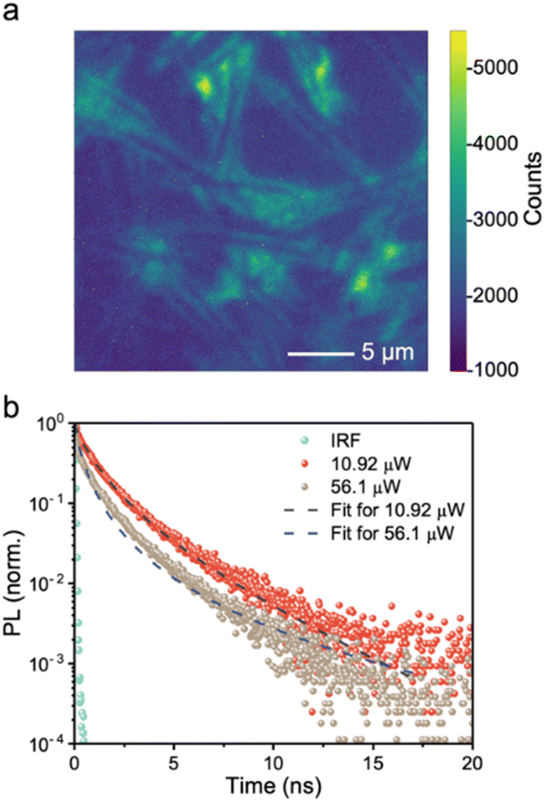 | ||
| Fig. 3 (a) Microscopy-PL image of BiSBr thin film sample. The bright-field optical micrograph and PL map of the sample were taken over exactly the same area. The optical micrograph is in black and white, while the PL map is shown in color, with the intensity of PL represented by the colorscale displayed. The PL map is superimposed over the optical micrograph. (b) Confocal microscopy-time-correlated single photon counting (TCSPC) measurements of BiSBr in air at 10.9 μW and 56.9 μW excitation laser power, along with the instrument response function (IRF) and fitted models (refer to Tables S5 and S6, ESI† for details). The excitation wavelength was 520 nm, with a repetition rate of 5 MHz, incident on the film side. | ||
Herein, we selected the brightest region on the PL map, and measured the PL decay at two excitation fluences. As shown in Fig. 3b, increasing the fluence led to a faster decay. This is consistent with transitioning the recombination regime from radiative to Auger-dominated, which occurs at high fluences. We fitted the PL decays measured at 10.9 μW and 56.9 μW excitation laser power using a phenomenological triexponential model, from which we estimated the average time constants to be 1.86 and 1.48 ns, respectively. More information can be found in Table S5, ESI,† and it can be seen in Fig. S10, ESI† that a very close fit was obtained to the measured data. We also fitted the PL decays using a model that accounts for surface and bulk recombination, as well as the diffusion of charge-carriers from the excitation spot (see ref. 68 and 69). The fits to the data are shown as dashed lines in Fig. 3b, and the parameter fits are provided in Table S6, ESI.† The effective total lifetimes, accounting for bulk and surface recombination, were 4.7 and 2.9 ns for 10.9 μW and 56.9 μW excitation measurements, respectively. The charge-carrier kinetics of BiSBr therefore justifies development in photovoltaics.
Band structure of BiSBr
To pave the way for future efforts to develop photovoltaic devices from BiSBr, we measured the band positions. For the valence band position, we used X-ray photoemission spectroscopy (XPS; performed under ultra-high vacuum) and photoelectron spectroscopy in air (PESA; performed in ambient air without any vacuum steps). From XPS, we could obtain the valence band to Fermi level offset (EVB − EF) by fitting a tangent to the primary edge of the valence band spectrum (Fig. 4a), which was 1.31 ± 0.07 eV. We determined the Fermi level position relative to vacuum level from macroscopic Kelvin Probe measurements of the samples in ambient air. The average value of the workfunction within 100 scans was 4.71 ± 0.09 eV (Fig. 4b). The ionization potential of BiSBr from XPS and Kelvin Probe measurements was therefore 6.0 ± 0.1 eV. We also determined the ionization potential directly from PESA measurements in air, and found it to be 5.93 eV (see Fig. 4c), which is within error of the measurements from XPS and Kelvin Probe. Furthermore, if we compare the EVB − EF to the bandgap of BiSBr (1.91 ± 0.06 eV), we can see that this material is weakly n-type.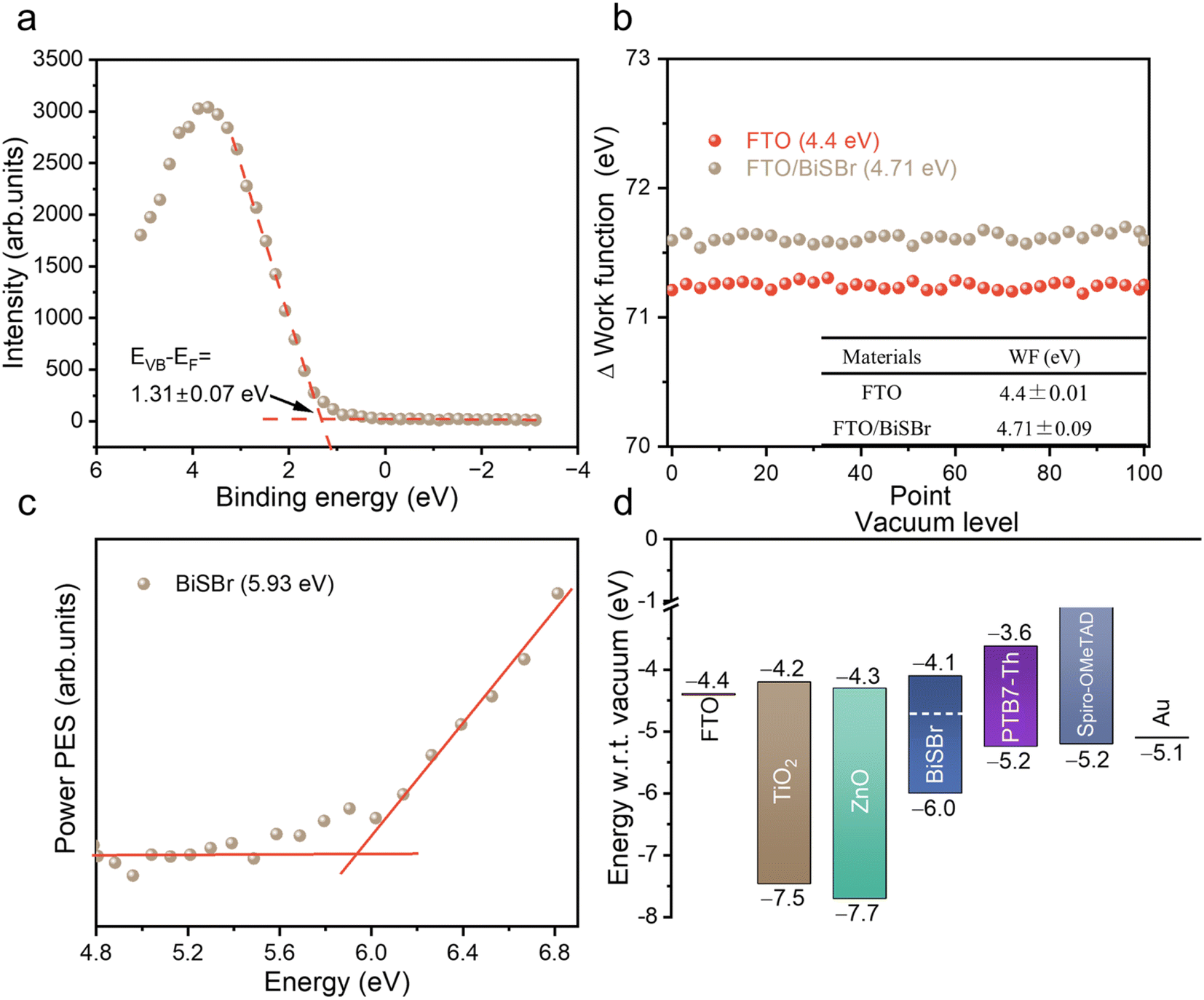 | ||
| Fig. 4 (a) Valence band spectrum from X-ray photoemission spectroscopy measurements of BiSBr thin films, showing our fit to the primary edge; (b) Kelvin probe measurements of the workfunction of BiSBr thin films deposited on FTO, as well as measurements of the FTO substrate. For each sample, 100 measurements were taken, and the average workfunction obtained, along with the uncertainty. (c) Photoemission spectroscopy in air (PESA) of BiSBr. (d) Schematic diagram of the band positions of BiSBr determined through photoemission spectroscopy, Kelvin probe and bandgap measurements compared with the band positions of common electron and hole transport layers.4,5 | ||
To determine the electron affinity, we subtracted the bandgap from the ionization potential, obtaining a value of 4.1 ± 0.1 eV. These conduction and valence band positions are very well aligned with common electron and hole transport layers, as shown in Fig. 4d. The wide variety of options available for feasible charge transport layers (CTLs) means that early device fabrication efforts can focus more on CTL materials with suitable morphologies (e.g., mesoporous structured) and surface energies for obtaining compact thin films of BiSBr. Furthermore, the band positions of BiSBr are well suited to carrying out H+ and CO2 reduction reactions, as well as the oxygen evolution reaction,14 which opens up another opportunity for BiSBr in terms of photocatalytic and photoelectrochemical applications. We add that the anisotropic structure of BiSBr could lead to variations in the band position along different faces, and this should be studied in greater detail in the future.
Conclusion
To conclude, we successfully synthesized phase-pure BiSBr thin films through a solution processing route using RoHS-compliant precursors, and a low-toxicity solvent. We found that annealing these materials at 250 °C for 10 min inside a N2-filled glovebox led to highly stoichiometric films (B:S:Br = 1.00:1.01:1.12). The phase-purity of these films was verified through X-ray diffraction and Raman scattering measurements, and we demonstrated the material to be stable in ambient air without encapsulation for at least 14 days, and were also more environmentally- and photo-stable than triple cation perovskite thin films. We determined the indirect bandgap to be 1.91 ± 0.06 eV, which matches the ideal bandgap for indoor light harvesting. Using the absorption coefficient spectrum we measured, we predicted that this material could reach up to 43.6% efficiency in IPVs. By estimating the PL lifetimes from both a phenomenological tri-exponential model, as well as a physically-relevant recombination-diffusion model, we found that the charge-carrier lifetime of BiSBr justifies its development in photovoltaics. From photoemission spectroscopy and Kelvin probe measurements, we determined the band positions to be 4.1 ± 0.1 eV (conduction band minimum) and 6.0 ± 0.1 eV (valence band maximum), meaning that BiSBr devices can be fabricated using standard test photovoltaic device structures. Thus, from the analyses of the bulk properties, this work demonstrates BiSBr to be a promising material for IPV applications, with potential to surpass the performance of the current incumbent technology (a-Si:H). Whilst the morphology requires optimization before realizing photovoltaics from BiSBr, the high surface area to volume ratio of current films may already be well suited to photocatalytic and photoelectrochemical applications, especially since the band positions are well suited to carrying out water splitting and CO2 reduction reactions.
Author contributions
X. G. synthesized the BiSBr thin films, took photographs, carried out XRD, UV-vis spectrophotometry characterizations, and analyzed received raw data. Y.-T. H. performed Raman scattering measurements and helped with the analysis of the results. H. L. conducted the theoretical calculations (supervised by A. W.), SEM and EDX measurements. J. Y., J. L. and N. G. conducted confocal microscopy measurements, supervised by A. R., and helped with result analysis. Y. L. measured and analyzed Kelvin Probe data, supervised by I. M. S. J. Z. measured and analyzed the PDS data. D. D. performed the PL measurements. H. Z. contributed guidance and suggestions to this work. R. L. Z. H. conceived of the project and supervised the work.Conflicts of interest
There are no conflicts to declare.Acknowledgements
We gratefully thank Prof. Aron Walsh (Imperial College London) for support on the computations made in this work, and Han Bin Cho (Hanyang University) for preparing the triple-cation perovskite thin films that we used here. The authors would like to thank UK Research and Innovation for a Frontier Grant (no. EP/X022900/1), awarded through the 2021 ERC Starting Grant scheme. In addition, the authors thank the Henry Royce Institute for funding through the Industrial Collaborative Programme, funded by the Engineering and Physical Sciences Research Council (EPSRC, no. EP/X527257/1). H. L. would like to acknowledge the use of the University of Oxford Advanced Research Computing (ARC) facility in carrying out this work (http://doi.org/10.5281/zenodo.22558). Additionally, this work used the ARCHER2 UK National Supercomputing Service (https://www.archer2.ac.uk). The authors also acknowledge use of characterization facilities within the David Cockayne Centre for Electron Microscopy, Department of Materials, University of Oxford, alongside financial support provided by the Henry Royce Institute (EPSRC no. EP/R010145/1). Y.-T. H. and R. L. Z. H. also acknowledge support from EPSRC grant no. EP/V014498/2. Y. L. and I. M. would like to acknowledge financial support from KAUST Office of Sponsored Research CRG10, by EU Horizon 2020 grant agreement no. 952911, BOOSTER, grant agreement no. 862474, RoLA-FLEX, and grant agreement no. 101007084 CITYSOLAR, as well as EPSRC (no. EP/T026219/1 and EP/W017091/1). S. J. Z. acknowledges support from the Polish National Agency for Academic Exchange within the Bekker program (grant no. PPN/BEK/2020/1/00264/U/00001). H. Z. Acknowledges funding from Iberdrola through the Energy for Future (E4F) Postdoctoral Fellowship (no. 101034297). R. L. Z. H. acknowledges support from the Royal Academy of Engineering through the Research Fellowships scheme (no. RF\201718\17101).References
- J. B. Li, V. Chawla and B. M. Clemens, Adv. Mater., 2012, 24, 720–723 CrossRef CAS PubMed.
- S. Hadke, M. Huang, C. Chen, Y. F. Tay, S. Chen, J. Tang and L. Wong, Chem. Rev., 2021, 122, 10170–10265 CrossRef PubMed.
- L. Meng, J. You and Y. Yang, Nat. Commun., 2018, 9, 5265 CrossRef CAS PubMed.
- X. Dai, P. Koshy, C. C. Sorrell, J. Lim and J. S. Yun, Energies, 2020, 13, 6335 CrossRef CAS.
- S. Nam, J. Seo, S. Woo, W. H. Kim, H. Kim, D. D. Bradley and Y. Kim, Nat. Commun., 2015, 6, 8929 CrossRef CAS PubMed.
- R. E. Brandt, J. R. Poindexter, P. Gorai, R. C. Kurchin, R. L. Z. Hoye, L. Nienhaus, M. W. Wilson, J. A. Polizzotti, R. Sereika and R. Zaltauskas, Chem. Mater., 2017, 29, 4667–4674 CrossRef CAS.
- V. Steinmann, R. E. Brandt and T. Buonassisi, Nat. Photonics, 2015, 9, 355–357 CrossRef CAS.
- D. Cahen, L. Kronik and G. Hodes, ACS Energy Lett., 2021, 6, 4108–4114 CrossRef CAS.
- D. Meggiolaro, S. G. Motti, E. Mosconi, A. J. Barker, J. Ball, C. A. R. Perini, F. Deschler, A. Petrozza and F. De Angelis, Energy Environ. Sci., 2018, 11, 702–713 RSC.
- A. M. Ganose, D. O. Scanlon, A. Walsh and R. L. Z. Hoye, Nat. Commun., 2022, 13, 4715 CrossRef CAS PubMed.
- R. E. Brandt, V. Stevanović, D. S. Ginley and T. Buonassisi, MRS Commun., 2015, 5, 265–275 CrossRef CAS.
- A. M. Ganose, C. N. Savory and D. O. Scanlon, Chem. Commun., 2017, 53, 20–44 RSC.
- R. L. Z. Hoye, J. Hidalgo, R. A. Jagt, J. P. Correa-Baena, T. Fix and J. L. MacManus-Driscoll, Adv. Energy Mater., 2022, 12, 2100499 CrossRef CAS.
- Y.-T. Huang, S. R. Kavanagh, D. O. Scanlon, A. Walsh and R. L. Z. Hoye, Nanotechnology, 2021, 32, 132004 CrossRef CAS PubMed.
- V. Pecunia, L. G. Occhipinti and R. L. Z. Hoye, Adv. Energy Mater., 2021, 11, 2100698 CrossRef CAS.
- I. Mathews, S. N. Kantareddy, T. Buonassisi and I. M. Peters, Joule, 2019, 3, 1415–1426 CrossRef CAS.
- H. S. Ryu, S. Y. Park, T. H. Lee, J. Y. Kim and H. Y. Woo, Nanoscale, 2020, 12, 5792–5804 RSC.
- M. M. Rathore, A. Ahmad, A. Paul and S. Rho, Comput. Networks, 2016, 101, 63–80 CrossRef.
- O. Inderwildi, C. Zhang, X. Wang and M. Kraft, Energy Environ. Sci., 2020, 13, 744–771 RSC.
- T. Ahmad and D. Zhang, Sustain. Cities Soc., 2021, 68, 102783 CrossRef.
- T. A. Kurniawan, M. H. D. Othman, X. Liang, H. H. Goh, P. Gikas, T. D. Kusworo, A. Anouzla and K. W. Chew, J. Environ. Manage., 2023, 338, 117765 CrossRef CAS PubMed.
- P. Harrop, Battery Elimination in Electronics and Electrical Engineering 2018-2028, IDTechEx, Cambridge, 2017 Search PubMed.
- P. Sparks, The route to a trillion devices, ARM, 2017 Search PubMed.
- H. Michaels, M. Rinderle, R. Freitag, I. Benesperi, T. Edvinsson, R. Socher, A. Gagliardi and M. Freitag, Chem. Sci., 2020, 11, 2895–2906 RSC.
- M. Li, F. Igbari, Z. K. Wang and L. S. Liao, Adv. Energy Mater., 2020, 10, 2000641 CrossRef CAS.
- Z. Jin, Z. Zhang, J. Xiu, H. Song, T. Gatti and Z. He, J. Mater. Chem. A, 2020, 8, 16166–16188 RSC.
- Y. Peng, T. N. Huq, J. Mei, L. Portilla, R. A. Jagt, L. G. Occhipinti, J. L. MacManus-Driscoll, R. L. Hoye and V. Pecunia, Adv. Energy Mater., 2021, 11, 2002761 CrossRef CAS.
- Y. Peng, F. Li, Y. Wang, Y. Li, R. L. Z. Hoye, L. Feng, K. Xia and V. Pecunia, Appl. Mater. Today, 2020, 19, 100637 CrossRef.
- A. Chakraborty, N. Pai, J. Zhao, B. R. Tuttle, A. N. Simonov and V. Pecunia, Adv. Funct. Mater., 2022, 32, 2203300 CrossRef CAS.
- I. Turkevych, S. Kazaoui, N. Shirakawa and N. Fukuda, Jpn. J. Appl. Phys., 2021, 60, SCCE06 CrossRef CAS.
- B. Al-Anesi, G. K. Grandhi, A. Pecoraro, V. Sugathan, N. Viswanath, H. Ali-Löytty, M. Liu, T.-P. Ruoko, K. Lahtonen, D. Manna, S. Toikkonen, A. Belén Muñoz-García, M. Pavone and P. Vivo, ChemRxiv, 2023 Search PubMed , preprint http://10.26434/chemrxiv-2023-nb5jj.
- A. M. Ganose, S. Matsumoto, J. Buckeridge and D. O. Scanlon, Chem. Mater., 2018, 30, 3827–3835 CrossRef CAS PubMed.
- A. M. Ganose, K. T. Butler, A. Walsh and D. O. Scanlon, J. Mater. Chem. A, 2016, 4, 2060–2068 RSC.
- N. T. Hahn, J. L. Self and C. B. Mullins, J. Phys. Chem. Lett., 2012, 3, 1571–1576 CrossRef CAS PubMed.
- N. T. Hahn, A. J. Rettie, S. K. Beal, R. R. Fullon and C. B. Mullins, J. Phys. Chem. C, 2012, 116, 24878–24886 CrossRef CAS.
- H. Kunioku, M. Higashi and R. Abe, Sci. Rep., 2016, 6, 32664 CrossRef CAS PubMed.
- Z. Ran, X. Wang, Y. Li, D. Yang, X.-G. Zhao, K. Biswas, D. J. Singh and L. Zhang, npj Comput. Mater., 2018, 4, 14 CrossRef.
- Y. Zhou, L. Wang, S. Chen, S. Qin, X. Liu, J. Chen, D.-J. Xue, M. Luo, Y. Cao and Y. Cheng, Nat. Photonics, 2015, 9, 409–415 CrossRef CAS.
- D. Quarta, S. Toso, R. Giannuzzi, R. Caliandro, A. Moliterni, G. Saleh, A. L. Capodilupo, D. Debellis, M. Prato and C. Nobile, Angew. Chem., 2022, 134, e202201747 CrossRef.
- W. Kohn and L. J. Sham, Phys. Rev., 1965, 140, A1133 CrossRef.
- J. W. Furness, A. D. Kaplan, J. Ning, J. P. Perdew and J. Sun, J. Phys. Chem. Lett., 2020, 11, 8208–8215 CrossRef CAS PubMed.
- G. Kresse and J. Hafner, Phys. Rev. B: Condens. Matter Mater. Phys., 1993, 47, 558 CrossRef CAS PubMed.
- G. Kresse and J. Furthmüller, Comput. Mater. Sci., 1996, 6, 15–50 CrossRef CAS.
- G. Kresse and J. Furthmüller, Phys. Rev. B: Condens. Matter Mater. Phys., 1996, 54, 11169 CrossRef CAS PubMed.
- G. Kresse and D. Joubert, Phys. Rev. B: Condens. Matter Mater. Phys., 1999, 59, 1758 CrossRef CAS.
- S. R. Kavanagh, vaspup2.0, https://github.com/kavanase/vaspup2.0, accessed June, 2023.
- W. Press, B. Flannery, S. Teukolski and W. Vetterling, Numerical Recipes, Cambridge University Press, Cambridge, 1986 Search PubMed.
- P. E. Blöchl, O. Jepsen and O. K. Andersen, Phys. Rev. B: Condens. Matter Mater. Phys., 1994, 49, 16223 CrossRef PubMed.
- A. M. Ganose, A. J. Jackson and D. O. Scanlon, J. Open Source Softw., 2018, 3, 717 CrossRef.
- C. L. McCarthy and R. L. Brutchey, Chem. Commun., 2017, 53, 4888–4902 RSC.
- L. Zhu, Y. Xie, X. Zheng, X. Yin and X. Tian, Inorg. Chem., 2002, 41, 4560–4566 CrossRef CAS PubMed.
- X. Jin, Y. Fang, T. Salim, M. Feng, S. Hadke, S. W. Leow, T. C. Sum and L. H. Wong, Adv. Funct. Mater., 2020, 30, 2002887 CrossRef CAS.
- G. Pawley, J. Appl. Crystallogr., 1981, 14, 357–361 CrossRef CAS.
- X. Wang, Z. Li, S. R. Kavanagh, A. M. Ganose and A. Walsh, Phys. Chem. Chem. Phys., 2022, 24, 7195–7202 RSC.
- W. Lou, M. Chen, X. Wang and W. Liu, Chem. Mater., 2007, 19, 872–878 CrossRef CAS.
- J. Ota and S. K. Srivastava, Cryst. Growth Des., 2007, 7, 343–347 CrossRef CAS.
- E. Furman, O. Brafman and J. Makovsky, Phys. Rev. B: Solid State, 1976, 13, 1703 CrossRef CAS.
- R. L. Z. Hoye, R. E. Brandt, A. Osherov, V. Stevanović, S. D. Stranks, M. W. Wilson, H. Kim, A. J. Akey, J. D. Perkins and R. C. Kurchin, Chem.–Eur. J., 2016, 22, 2605–2610 CrossRef CAS PubMed.
- R. A. Jagt, T. N. Huq, S. A. Hill, M. Thway, T. Liu, M. Napari, B. Roose, K. Gałkowski, W. Li and S. F. Lin, ACS Energy Lett., 2020, 5, 2456–2465 CrossRef CAS.
- A. Sadhanala, F. Deschler, T. H. Thomas, S. E. Dutton, K. C. Goedel, F. C. Hanusch, M. L. Lai, U. Steiner, T. Bein and P. Docampo, J. Phys. Chem. Lett., 2014, 5, 2501–2505 CrossRef CAS PubMed.
- A. Naeem, F. Masia, S. Christodoulou, I. Moreels, P. Borri and W. Langbein, Phys. Rev. B: Condens. Matter Mater. Phys., 2015, 91, 121302 CrossRef.
- L. Yu and A. Zunger, Phys. Rev. Lett., 2012, 108, 068701 CrossRef PubMed.
- K. L. Wang, H. Lu, M. Li, C. H. Chen, D. Bo Zhang, J. Chen, J. J. Wu, Y. H. Zhou, X. Q. Wang and Z. H. Su, Adv. Mater., 2023, 2210106 CrossRef CAS PubMed.
- R. Jaramillo, M.-J. Sher, B. K. Ofori-Okai, V. Steinmann, C. Yang, K. Hartman, K. A. Nelson, A. M. Lindenberg, R. G. Gordon and T. Buonassisi, J. Appl. Phys., 2016, 119, 035101 CrossRef.
- D. Y. Yu, H. E. Hoster and S. K. Batabyal, Sci. Rep., 2014, 4, 4562 CrossRef PubMed.
- D. Tiwari, F. Cardoso-Delgado, D. Alibhai, M. Mombru and D. J. Fermín, ACS Appl. Energy Mater., 2019, 2, 3878–3885 CrossRef CAS.
- W. Yang, J. H. Kim, O. S. Hutter, L. J. Phillips, J. Tan, J. Park, H. Lee, J. D. Major, J. S. Lee and J. Moon, Nat. Commun., 2020, 11, 861 CrossRef CAS PubMed.
- J. R. Poindexter, R. L. Z. Hoye, L. Nienhaus, R. C. Kurchin, A. E. Morishige, E. E. Looney, A. Osherov, J.-P. Correa-Baena, B. Lai, V. Bulović, V. Stevanović, M. G. Bawendi and T. Buonassisi, ACS Nano, 2017, 11, 7101–7109 CrossRef CAS PubMed.
- R. L. Z. Hoye, L. C. Lee, R. C. Kurchin, T. N. Huq, K. H. L. Zhang, M. Sponseller, L. Nienhaus, R. E. Brandt, J. Jean, J. A. Polizzotti, A. Kursumović, M. G. Bawendi, V. Bulović, V. Stevanović, T. Buonassisi and J. L. MacManus-Driscoll, Adv. Mater., 2017, 29, 1702176 CrossRef PubMed.
Footnote |
| † Electronic supplementary information (ESI) available: Supporting X-ray diffraction measurements and analysis, UV-vis measurements, fitting of the Urbach tail, density of states calculations, scanning electron microscopy images and PL lifetime fitting. See DOI: https://doi.org/10.1039/d3ta04491b |
| This journal is © The Royal Society of Chemistry 2023 |