
 Open Access Article
 This Open Access Article is licensed under a
 Creative Commons Attribution 3.0 Unported Licence
Revani diffusion model in Cu(In,Ga)Se2
Diego
Colombara
 *a,
Billy J.
Stanbery
b and
Giovanna
Sozzi
c
*a,
Billy J.
Stanbery
b and
Giovanna
Sozzi
c
aUniversità degli Studi di Genova, via Dodecaneso 31, 16146 Genova, Italy. E-mail: diego.colombara@bath.edu
bColorado School of Mines, 1301 19th St, Hill Hall, Golden, CO 80401, USA
cUniversità degli Studi di Parma, Parco Area delle Scienze, 181/A, 43124 Parma, Italy
First published on 27th November 2023
Abstract
The commercial attractiveness of Cu(In,Ga) (S,Se)2 (CIGS) photovoltaics is still curtailed by the R&D gap that separates it from silicon. Overcoming the gap requires the pursuit of strategic approaches, leaving plenty of room for R&D at both industrial and lab scale. Yet, its technological progress hinges on our understanding of the diffusion phenomena that occur during and after the absorber growth, particularly in combination with alkali metal doping. This contribution introduces a simplified model of atomic diffusion in CIGS based on insights drawn from recent and older (but crucial) literature. The concept of anisotropy-induced fluctuations emerges. We hypothesize that grain-dependent inhomogeneities arise in CIGS devices because of crystallographic dependent alkali metal diffusivities. Numerical simulations reveal that inhomogeneous doping density and CdS buffer layer thickness may impair the device performance by up to more than 1% absolute efficiency.
1. Introduction
At 23.6%, CIGS cells are the most efficient among the commercially available polycrystalline thin film technologies.1 Very high efficiencies are attained with two distinct deposition strategies, both of which are employed industrially for module manufacturing: reactive annealing of metal precursors,2 and elemental co-evaporation.3 CIGS is also deposited on flexible substrates such as stainless steel foils and even polymers.4 This is particularly attractive for building-integrated applications, which is expected to become compulsory for new constructions in Europe and certain US states.One appealing prospect is to deploy CIGS as a low-bandgap partner to higher bandgap semiconductors such as metal halide perovskites,5 with the aim of developing tandem cells with a Shockley–Queisser (SQ) efficiency limit of 46%.
However, the high record efficiencies at laboratory cell scale are still lagging 3.4 percent points behind the competitive silicon technology. This efficiency gap is also transferred at module level,6 mainly due to resistive losses in the front transparent conductive oxide (TCO) that become important when passing from small to large areas. In tandem applications, utilizing low-bandgap CIGS with reduced short circuit photocurrent density mitigates significantly the impact of these TCO resistive losses.
A long-sought approach to solve this conundrum is to develop wider-gap CIGS, as this would increase the voltage and decrease the electrical current, hence the resistive losses in the TCO. Efficient wider-gap CIGS would also serve as a stable top junction in tandem cells. This so-called chalcopyrite material allows bandgap widening by simply increasing the relative concentration of gallium compared to indium or sulfur compared to selenium. Nevertheless, achieving highly efficient wider-gap CIGS cells has been very challenging, due to significant voltage losses.7–9 Recently, advances have been achieved on both S-rich10 and Ga-rich11 CIGS cells through processing changes to minimize the scale of spatially varying disorder – a major root cause of voltage deficit – and silver alloying as an effective strategy to improve crystal quality.
Conceivably, if recent advances in wider-gap CIGS devices, as well as trends and limitations of today's narrow-gap CIGS devices can be understood, and the path towards SQ parity can be identified, holistic insights into the material will be learned, for the benefit of the technology as a whole.12 Herein, a revani† model of atomic diffusion is presented to account for both recent and older overlooked evidence and suggest the crucial link to CIGS device performance.
2. Do we really understand alkali metal doping?
The efficiency deficit of record CIGS from the viewpoint of carrier management (expressed as the product ff × VOC, fill factor times open circuit voltage13) is approximately 24% relative to SQ. This deficit is larger for CdTe (conservative estimate: 28% relative), but considerably lower for silicon (ca. 16% relative). Therefore, research is being devoted to understanding its origin, particularly relating to VOC.Voltage losses in record cells have long been attributed to electrostatic potential fluctuations,14 but SRH recombination cannot be excluded although it is hard to detect defects potentially acting as recombination centres.15
Voltage deficit in record CIGS has been shrinking since the introduction of alkali (Ak) metal doping in 1993. Ak metals are typically incorporated by diffusion of Na from soda-lime glass substrates and/or post-deposition treatments (Ak-PDT) performed on the absorber's surface after growth3,4. The beneficial effect of Ak-PDT on VOC has been ascribed to reduced fluctuations,16 decreased defect density at the interface,17 and grain boundaries.18 There is evidence that Ak-PDT reduces nonradiative recombination originating from grain boundaries,19 also in combination with oxygen.20 Yet, the underlying diffusion interplay between Ak dopants and matrix atoms in CIGS21–23 (including its copper deficient surface layer, CDL24), cannot be excluded to play an important role within the interior of the grains, given that photoluminescence analyses point to Ak reducing electrostatic potential fluctuations even in CIGS free from grain boundaries.25
CIGS is a complex playground for exotic atomic diffusion phenomena that we are just now starting to grasp.26,27 This contribution simplifies the picture with a wet sponge cake called revani, where the porous cake itself is the CIGS lattice and the wet syrup is the Ak metal dopant, particularly the sodium.
3. Revani model of atomic diffusion interdependence
This model (Fig. 1) is a simplification of a new theory of atomic diffusion illustrated in ref. 26 that is based on experimental evidence from Na-doped Cu(In,Ga)Se2 (ref. 22 and 28) and is partially supported by a computational study.29 Starting assumption for the theory is that diffusion of sodium can take place via both vacancy and interstitial sites, according to the known Frank–Turnbull mechanism (FT).30 Although the FT mechanism has never been confirmed experimentally in CIGS,31 its likelihood is supported implicitly by computational studies of atomic migration.32,33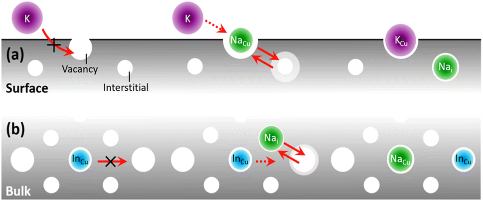 | ||
| Fig. 1 Revani model of atomic diffusion in CIGS. A dopant (e.g. Na, green) within CIGS may enhance (a) surface/boundary diffusivity (e.g. of another foreign atom like K, purple4) and/or (b) grain interior/bulk diffusivity (e.g. of matrix atoms like In, cyan22), if its own diffusion occurs via the Frank–Turnbull (FT) mechanism and is faster than those of foreign/matrix atoms in CIGS. The two red arrows in the middle section signify the FT mechanism of a Na atom diffusing to and from substitutional/interstitial sites. | ||
In essence, the theory argues that the close proximity between atomic surfactants34,35 (e.g. sodium dopant atoms) and matrix anions (selenium) lowers the bond strength between the matrix anions and the matrix cations (copper, indium and gallium), thus decreasing the energy barrier for atomic migration. The end result is a migration catalysis: the spatial distribution of matrix atoms in the material (i.e. from the atomic to the microscopic level) may more easily approach the thermodynamic limit by taking advantage of faster diffusion kinetics. This migration catalysis may take place, to different extents, at CIGS surfaces and grain boundaries (Fig. 1a) or grain interiors (Fig. 1b).
(a) Revani cake soaking stage, Fig. 1a. At interfaces and grain boundaries the presence of sodium can enhance ion exchange and induce incorporation of impurity atoms such as potassium and rubidium during Ak-PDT.
(b) Revani cake squeezing stage, Fig. 1b. In the bulk of CIGS grains, sodium may ease the attainment of the equilibrium elemental distribution, i.e. the CIGS-OVC phase separation, with the latter destined to occupy surfaces and boundaries.
It follows from this model that the respective localization of sodium and other elements at CIGS interfaces, grain boundaries or interiors is highly interdependent.36 The interdependence occurs because the migration route of sodium overlaps with the migration routes of the other elements, leading to mutually perturbed hopping events. The exact outcome of this interdependence originates from an interplay between process temperature and local composition (chemical potentials37), jointly dictating the concentration of point defects, the frequency of the event, and hence the likelihood of each individual jump in the presence of the thermodynamic driving force represented by phase segregation.
4. Fingerprints of the revani model from the literature
Since the dawn of CIGS research, it is known that film texture and grain size vary significantly, depending on the chemical composition during growth and especially on the presence or absence of Ak metal impurities. Ironically, crucial supporting hints come from the very first study on sodium doping dating back to 1993.38 X-ray diffractograms of CIS films grown on soda-lime glass substrates showed pronounced crystallographic orientation such that “virtually no other peak than the (112)” was seen for uncoated substrates. The effect was confirmed by other groups worldwide39–41 and linked to sodium incorporation, but the broader implications have been underappreciated. Interestingly, changes in preferred orientation from (112) to (220) were reported in the presence of sodium if the deposition temperature is increased up to 570 °C,42 hinting to a transition temperature between diffusion regimes.4.1. Origin of anisotropy-induced fluctuations
If sodium diffusion occurs (also) through interstitials, as assumed in the revani model, different crystallographic orientation of the grains become a possible source of property fluctuations at the microscale. In fact, grains with (220) or (102) planes oriented perpendicular to the substrate may convey a higher concentration of mobile Na+ cations, due to the higher concentration of interstitial sites they contain, compared to e.g. (112) oriented grains, as exemplified in Fig. 2a. Certain facets are expected to grow at a higher rate than others, due to higher orientation-dependent atomic diffusivity induced by sodium. The proposed FT-induced anisotropy of sodium migration in CIGS complements previous studies on spontaneous surface faceting43–46 and is consistent with recent findings where preferential sodium diffusion was reported to occur through the (220)/(204) crystallographic direction.47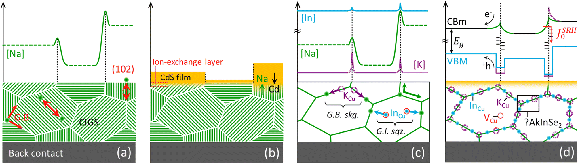 | ||
| Fig. 2 Possible anisotropy-induced fluctuations caused by orientation-dependent diffusivity of sodium in CIGS, as simplified by the revani model. (a) If sodium diffuses via the FT mechanism, crystallographic directions displaying a larger concentration of interstitial sites (e.g. (220) and (102) shown by the red double arrows) will act as preferential pathways for sodium diffusion and for indium-gallium mass transport, as displayed here in a non-textured polycrystalline film. Hence, the growth of various grains is expected to be self-selected, leading to textured films with interstitial-poor (112) planes parallel to the sodium-containing substrate. Likewise, the concentration of sodium from one grain to another may vary as a result of orientation dependent uptake of extrinsic dopant, leading to granularity of carrier density at the length scale of grain size. (b) The preferential diffusion of sodium along certain crystallographic directions implies an effectively larger sodium availability for ion–exchange reactions at the surface of those grains oriented with (112) planes perpendicular to the substrate, such that it may affect buffer layer nucleation and growth when this is done by chemical bath deposition, as observed by Witte et al.48 (c) Revani soaking (skg.) and squeezing (sqz.) stages, exemplified by uptake of potassium atoms at CIGS grain boundaries (GB) through ion exchange by sodium (both identified at G.B.49), and by removal of InCu donors from grain interior (GI) towards GBs. (d) Electronic consequences of the revani model onto the band structure of CIGS across GBs: bandgap widening at the GBs results from a lowering of the valence band maximum and a lift of the conduction band minimum following the compositional alterations. Such a band structure effectively repels photogenerated electron–hole pairs from defect-rich GB regions otherwise responsible for Schockley–Read–Hall recombination, as suggested by Keller et al.50 | ||
4.2. Implications for doping density fluctuations
The model implies lateral step fluctuations of acceptor concentration. Even though the impact of these inhomogeneities on device performance appears negligible for highly efficient narrow-gap CIGS cells,51–53 it may still be a problem for modules and wider gap CIGS.4.3. Implications for potential-induced degradation (PID)
Sodium diffusion is the most likely culprit for PID in CIGS, a module performance degradation that is common to all PV technologies.54 PID occurs when a high voltage forms between the solar cells in the module and the module frame, notably when numerous modules are connected in series to attain a high voltage output while minimising resistance losses. In CIGS, sodium is thought to electromigrate and impair the p–n junction and/or corrode the TCO contact.55,56 Granularity in the sodium accumulation was reported by Harvey et al.,57 suggesting preferential diffusion through certain grains that may be compatible with the revani model, even though the authors attribute the effect to grain boundary diffusion. The model may be tested experimentally by assessing the resilience to PID of cells whose CIGS absorber was deliberately grown with different preferential orientations.47 It is worth noting that the main CIGS PV manufacturers have overcome PID issues by employing barriers that prevent sodium diffusion from substrate, and encapsulant glass slabs during operation.4.4. Implications for buffer thickness fluctuations
Different sodium availability from grain to grain, or facet to facet, would also lead to a different extent of ionic exchange via the revani model, as shown in Fig. 2b. This scenario is consistent with recent findings revealing that CdS and Zn(O,S) buffer growth by chemical bath deposition is impaired on as-formed (112) CIGS facets48,58, where sodium availability through the interstitial route is less likely. Although the effect may be due to other differences in surface energetics, the revani hypothesis should be tested.4.5. Implications for inter/intra-grain fluctuations
The soaking stage (Fig. 2c, G.B. skg.) accounts for the intake of heavier Ak atoms favoured over sodium,4,59–62 which results in passivation due to bandgap widening at the grain boundary (Fig. 2d). Simulations have shown that even in the presence of high concentrations of defects at grain boundaries, the performance of the cell improves if the energy gap at the grain boundaries is sufficiently large compared to that of the grain interior.63 The intake of heavier Ak ions may occur by displacement of sodium ions (i.e. by exchange), or by a concerted movement of a sodium ion from its substitutional position to an interstitial site and concomitant incorporation of the heavier Ak ion into the emptied copper site (i.e. by FT mediation). This stage would also explain why a potassium-enriched surface is more prone to exchange potassium for cadmium, accounting for the improved CIGS/CdS heterojunction in K-doped films.4The squeezing stage (Fig. 2c, G.I. sqz.) accounts for sodium-induced migration of InCu antisite donors to the grain boundaries, thus decreasing compensation in the bulk (increasing the relative share of copper vacancies in the grains64,65) and turning the boundaries indium-rich (adding to bandgap widening) at the same time. This could explain why Na-doping increases the net acceptor concentration in CIGS,66 without excluding a concomitant increase of copper vacancies within the grains, according to the model by Yuan et al.67 (Fig. 2d), which is supported by the recent detection of sparse Cu-rich GBs even in nominally Cu-poor films.68
The combined effect is consistent with the general decrease of electrostatic potential fluctuations and may explain why sodium doping happens to be essential in the first place. In 2018, highly efficient single crystal devices were obtained for the first time in the history of CIGS. Decisively, these were fabricated with epitaxial absorbers subject to NaF and KF-PDTs.69 Such a fact demonstrates that good CIGS optoelectronic quality can indeed be attained even in the absence of grain boundaries, a conundrum that took many years to unravel!
5. Numerical simulations
Since the hypothesized fluctuations have a common root cause, we conduct numerical simulations at the device level to analyse how the varying thickness of the CdS buffer layer, along with the presence of fluctuating doping density in the underlying CIGS, affects the behaviour of the solar cell.The cell is simulated with the Synopsys Sentaurus-TCAD suite. The current–voltage characteristics of the cell is calculated by solving the Poisson and continuity equations for electrons and holes in a coupled manner, using the drift–diffusion model, and incorporating the effects of non-radiative recombination in the various layers through the Shockley–Read–Hall model. The behavior of the illuminated cell is computed by illuminating it with the AM1.5G spectrum and employing the experimental complex refractive indices of the various layers for the calculation of optical generation and reflection.70,71 The Transfer Matrix Method (TMM) is employed to analyze the behavior of the solar cells as the light passes through its layers. In each layer, the optical intensity is determined by evaluating the electric field amplitudes of both forward- and backward-propagating waves, considering the optical properties of the material, which are described by the complex refractive index. Afterwards, the optical generation is computed from the calculated optical intensity and wavelength-dependent absorption coefficient.
Fig. 3 depicts the two grains cell model following the standard configuration of CIGS cell, i.e., from top to bottom, MgF2 anti-reflecting coating, Aluminum doped ZnO window, high-resistive ZnO, CdS buffer and CIGS absorber. In particular, in grain A, the thickness of CdS, and the doping of the underlying CIGS are fixed and set at 40 nm and 1016 cm−3, respectively, while in grain B, they can vary. Similar to the ZSW cell, we also consider a MgF2 antireflective coating with a thickness of 100 nm to reduce reflection at the cell surface. We simulated the two-dimensional cross section of the cell in the red frame.
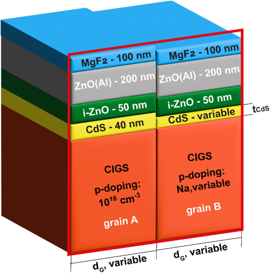 | ||
| Fig. 3 Schematic representation of the two-grains CIGS solar cell model (not to scale) employed to simulate the effects on device performance of anisotropy-induced fluctuations such as grain-dependent CdS buffer thickness and p-type doping. | ||
The main properties of the different layers and interfaces used in the simulation are summarized in Table 1. More details about simulations and material parameters can be found in our previous works.72
| AZO | i-ZnO | CdS | CIGS | |
|---|---|---|---|---|
| E g/eV | 3.3 | 3.3 | 2.4 | Graded |
| Thickness/nm | 200 | 50 | 40 nm/variable | 2300 |
| Doping/cm−3 | 5 × 10¹⁹ | 1017 | 1017 | 1016/variable |
| μ e (μh)/cm2 V−1 s−1 | 100 (25) | |||
| τ e (τh)/ns | 10 (0.01) | 10 (0.01) | 33 (0.01) | 250 (250) |
| CBO/eV | −0.2 | 0.1 | ||
First and foremost, we simulate a reference cell characterized by a constant buffer layer thickness and uniform CIGS doping throughout the grains, i.e., same tCdS = 40 nm, and acceptor density NA = 1016 cm−3 in both grain A and B, replicating a ZSW cell with an efficiency > 22%.3
The ZSW cell features a double-graded [Ga]/([Ga] + [In]) (GGI) composition CIGS layer, so we include the measured GGI profile of the highest efficiency cell shown in 73 within the CIGS layer. This allows to account for the varying bandgap grading in the CIGS layer and related optical coefficients that depend on the GGI and position, as illustrated in 74. The IV curve is also influenced by the alignment of the conduction bands at the hetero-interfaces, as shown in 75. In our simulations, we have considered a conduction band offsets (CBO) of 0.1 eV, creating a spike (i.e., the conduction band at the CIGS side is lower than that at the CdS side) at the CdS/CIGS interface, and 0.2 eV, forming a cliff (i.e., the conduction band at the ZnO side is lower than that at the CdS side) at the ZnO/CdS interface.
Furthermore, we assume ideal heterointerfaces, which entails zero recombination velocity. This choice was made to direct our attention specifically towards assessing the impact of variations of doping and CdS thickness on cell performance.
The parameters of the simulated reference cell closely match those of the 22% efficient CIGS cell fabricated by ZSW, as summarised in Table 2.
| V OC/V | J SC/mA cm−2 | ff/% | η/% | |
|---|---|---|---|---|
| ZSW | 0.744 | 36.70 | 80.50 | 22.00 |
| Simulation | 0.744 | 36.75 | 80.53 | 22.03 |
To examine how changes in the CdS thickness and doping levels within the CIGS layer might affect the cell's performance, our approach simulates two grains of the cell (cf.Fig. 3): in grain A, we maintain a uniform CdS thickness of 40 nm and CIGS doping density of 1016 cm−3, as in the reference cell. In grain B, we set either a CdS thickness tCdS = 30 nm with a CIGS doping density, NA, ranging between 1015 cm−3 and 1016 cm−3 (referred to as “scenario I”), or tCdS = 50 nm with NA ranging from 1016 cm−3 to 1017 cm−3 (denoted as “scenario II”).
Moreover, to determine if the impact of inhomogeneities can vary with grain size, simulations were performed for each combination of tCdS and NA using three different grain sizes, dG, of 0.25 μm, 0.5 μm, and 1 μm.
Fig. 4 shows the results of numerical simulations performed with varying tCdS against the CIGS doping level in grain B, NA, with each distinct curve corresponding to different grain sizes (denoted as dG). Each plot can be divided into two distinct regions: region I displays findings corresponding to scenario I, while region II presents results from scenario II.
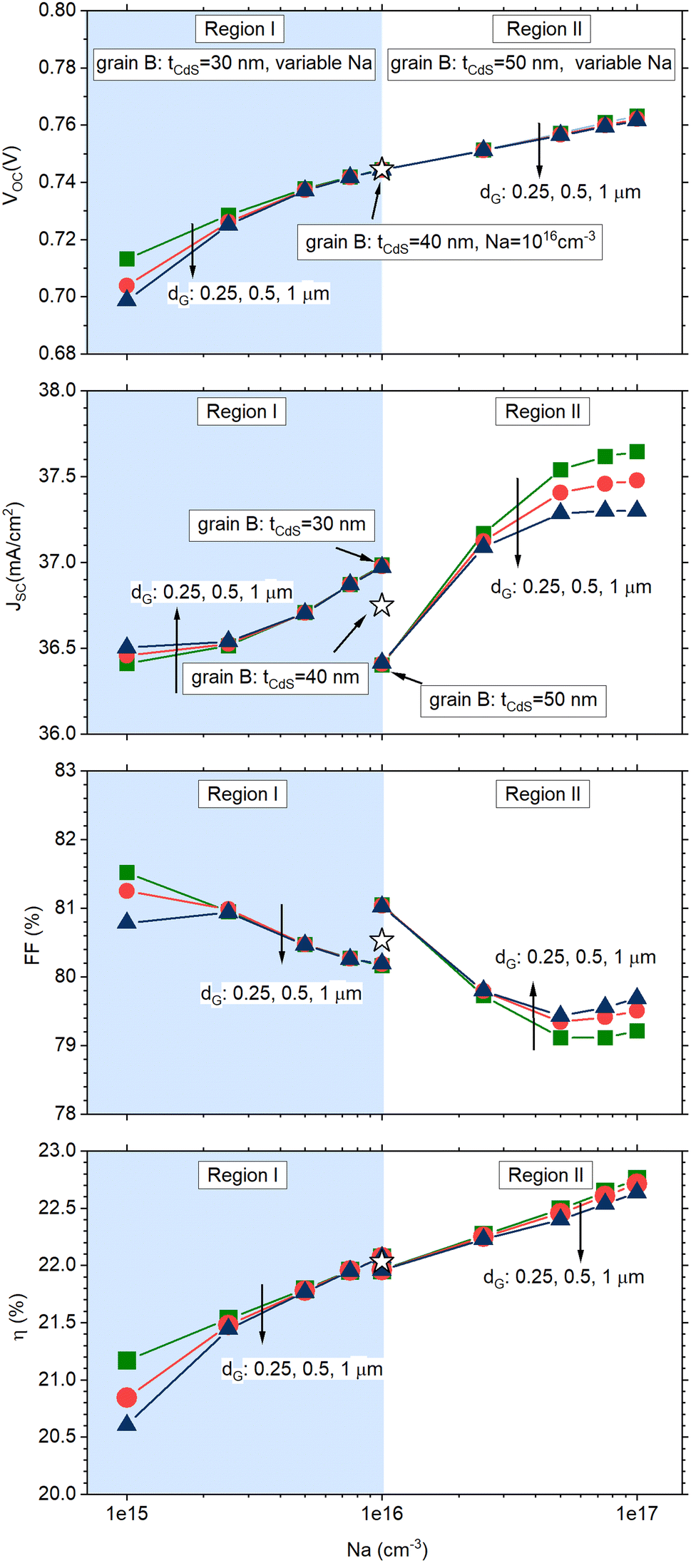 | ||
| Fig. 4 Simulated solar cell parameters for the solar cell sketched in Fig. 3. In all simulations, grain A has a uniform CdS thickness of 40 nm and CIGS doping density of 1016 cm−3 (star symbol in the figures). Region I displays results for the cell in which grain B has tCdS = 30 nm and variable CIGS doping density (1015 cm−3 ≤ NA ≤ 1016 cm−3); region II displays results for the cell in which grain B has tCdS = 50 nm and variable CIGS doping density (1016 cm−3 ≤ NA ≤ 1017 cm− 3). Different curves represent grain sizes with dimensions dG = 0.25, 0.5, 1 μm (square, circle, triangle symbols). | ||
The cell parameters of the reference cell, characterized by grains with uniform CdS thickness of 40 nm and CIGS doping of 1016 cm−3, are represented by the star symbol and are positioned midway between region I and region II.
Concerning the trends exhibited by the simulated cell parameters, the observed behaviours stem from a combination of electrical and optical factors.
Specifically, an increased thickness of the CdS layer decreases charge carrier generation within the CIGS layer, consequently affecting JSC.
This phenomenon is readily apparent in Fig. 4b for a doping level in grain B set at NA = 1016 cm−3: in this case, JSC exhibits the highest current value at tCdS = 30 nm while a lower value is observed at tCdS = 50 nm.
Conversely, a higher doping level in the CIGS layer enhances VOC by reducing non-radiative recombination processes (Fig. 4a), also enhancing JSC (Fig. 4b).
As a result of the combined influence of these factors, the cell efficiency curve exhibits a variation of over 1% in absolute efficiency, with a more pronounced impact observed in the case of larger grain sizes, dG.
The relationship between grain size and efficiency variation suggests that the portion of the grain with doping and CIGS thickness deviations has a greater influence compared to the portion with expected values.
If we visualize a cell containing thousands of grains resembling the ones being simulated, the simulations indicate that these deviations have a growing significance when dealing with larger grains and areas of non-uniformity that are similar to the homogeneous regions.
6. Conclusions
The evolution of CIGS solar cell performance over the years can be traced back to key technological innovations that improved the absorber's optoelectronic properties. Among these, Ak metal doping-especially sodium-has undeniably played the lion's share to success. Here, a revani (wet sponge cake) model of atomic diffusion, with soaking and squeezing stages, is proposed as a simple unifying concept to account for a number of unsettled experimental facts. The proposed micro-scale anisotropy-induced fluctuations, if confirmed, may account for bandgap tailing and voltage deficit in CIGS cells and/or modules. We encourage the community to test these hypotheses.Conflicts of interest
There are no conflicts of interest to declare.Acknowledgements
DC wishes to thank the organisers and attendees of the 49th IEEE Photovoltaics Specialists Conference (PVSC) held in June 2022 in Philadelphia for their interest on an earlier version of this study76 and for fruitful discussions. We would like to thank Susanne Siebentritt (U. of Luxembourg), Hossam Elanzeery (Avancis GmbH), Nicoleta Nicoara and Sascha Sadewasser (INL, Portugal), Luis Pazos-Outón (Google Inc.), Stefano Rampino, Edmondo Gilioli, and Massimo Mazzer (CNR IMEM, Italy) for valuable discussions. This research was funded by the University of Genova and Compagnia di San Paolo through the Curiosity Driven and Promoting Competitiveness schemes, and by the Italian Ministry of University and Research through the LEGACY (healing wide-gap chalcopyrite, grant No. 20223ZP4WP) project of national relevance (PRIN 2022), under the PE3 Condensed Matter Physics sector.References
- M. A. Green, et al., Solar cell efficiency tables (version 62), Prog. Photovolt.: Res. Appl., 2023, 31(7), 651–663, DOI:10.1002/pip.3726.
- M. Nakamura, K. Yamaguchi, Y. Kimoto, Y. Yasaki, T. Kato and H. Sugimoto, Cd-Free Cu(In,Ga)(Se,S)2 Thin-Film Solar Cell With Record Efficiency of 23.35, IEEE J. Photovolt., 2019, 9(6), 1863–1867, DOI:10.1109/JPHOTOV.2019.2937218.
- P. Jackson, R. Wuerz, D. Hariskos, E. Lotter, W. Witte and M. Powalla, Effects of heavy alkali elements in Cu(In,Ga)Se2 solar cells with efficiencies up to 22.6, Phys Status Solidi Rapid Res Lett., 2016, 10(8), 583–586, DOI:10.1002/pssr.201600199.
- A. Chirilă, et al., Potassium-induced surface modification of Cu(In,Ga)Se2 thin films for high-efficiency solar cells, Nat. Mater., 2013, 12(12), 1107–1111, DOI:10.1038/nmat3789.
- M. Jošt, et al., 21.6%-Efficient Monolithic Perovskite/Cu(In,Ga)Se2 Tandem Solar Cells with Thin Conformal Hole Transport Layers for Integration on Rough Bottom Cell Surfaces, ACS Energy Lett., 2019, 4(2), 583–590, DOI:10.1021/acsenergylett.9b00135.
- V. Bermudez and A. Perez-Rodriguez, Understanding the cell-to-module efficiency gap in Cu(In,Ga)(S,Se) 2 photovoltaics scale-up, Nat. Energy, 2018, 3(6), 466–475, DOI:10.1038/s41560-018-0177-1.
- M. A. Contreras, et al., Wide bandgap Cu(In,Ga)Se2 solar cells with improved energy conversion efficiency, Prog. Photovolt.: Res. Appl., 2012, 20(7), 843–850, DOI:10.1002/pip.2244.
- F. Larsson, et al., Record 1.0 V open-circuit voltage in wide band gap chalcopyrite solar cells, Prog. Photovolt.: Res. Appl., 2017, 25(9), 755–763, DOI:10.1002/pip.2914.
- M. Sood, et al., Passivating Surface Defects and Reducing Interface Recombination in CuInS2 Solar Cells by a Facile Solution Treatment, Sol. RRL, 2021, 5(4), 2100078, DOI:10.1002/solr.202100078.
- S. Shukla, et al., Carrier recombination mechanism and photovoltage deficit in 1.7-eV band gap near-stoichiometric Cu(In,Ga)S2, Phys. Rev. Mater., 2021, 5(5), 055403, DOI:10.1103/PhysRevMaterials.5.055403.
- T. Nishimura, A. Doi, J. Chantana, A. Mavlonov, Y. Kawano and T. Minemoto, Silver-alloyed wide-gap CuGaSe2 solar cells, Sol. Energy, 2021, 230, 509–514, DOI:10.1016/j.solener.2021.10.055.
- S. Ishizuka, CuGaSe2 Thin Film Solar Cells: Challenges for Developing Highly Efficient Wide-Gap Chalcopyrite Photovoltaics, Phys. Status Solidi A, 2019, 216(15), 1800873, DOI:10.1002/pssa.201800873.
- A. Polman, M. Knight, E. C. Garnett, B. Ehrler and W. C. Sinke, Photovoltaic materials: Present efficiencies and future challenges, Science, 2016, 352(6283), aad4424, DOI:10.1126/science.aad4424.
- S. Siebentritt, What limits the efficiency of chalcopyrite solar cells?, Sol. Energy Mater. Sol. Cells, 2011, 95(6), 1471–1476, DOI:10.1016/j.solmat.2010.12.014.
- F. Werner, et al., Alkali treatments of Cu(In,Ga)Se2 thin-film absorbers and their impact on transport barriers, Prog. Photovolt.: Res. Appl., 2018, 26(11), 911–923, DOI:10.1002/pip.3032.
- S. A. Jensen, et al., Beneficial effect of post-deposition treatment in high-efficiency Cu(In,Ga)Se2 solar cells through reduced potential fluctuations, J. Appl. Phys., 2016, 120(6), 063106, DOI:10.1063/1.4960344.
- K. F. Tai, R. Kamada, T. Yagioka, T. Kato and H. Sugimoto, From 20.9 to 22.3% Cu(In,Ga)(S,Se)2 solar cell: Reduced recombination rate at the heterojunction and the depletion region due to K-treatment, Jpn. J. Appl. Phys., 2017, 56(8S2), 08MC03, DOI:10.7567/JJAP.56.08MC03.
- S. Karki, P. Paul, G. Rajan, A. Rockett, A. Arehart and S. Marsillac, Characterization of Electronic Defects in RbF Treated CIGS Solar Cells, Presented at the 7th World Conference on Photovoltaic Energy Conversion, IEEE, Waikoloa, 2018 Search PubMed.
- S. Siebentritt, et al., Heavy Alkali Treatment of Cu(In,Ga)Se2 Solar Cells: Surface versus Bulk Effects, Adv. Energy Mater., 2020, 10(8), 1903752, DOI:10.1002/aenm.201903752.
- F. Babbe, et al., Vacuum-Healing of Grain Boundaries in Sodium-Doped CuInSe2 Solar Cell Absorbers, Adv. Energy Mater., 2023, 13(17), 2204183, DOI:10.1002/aenm.202204183.
- H. Rodriguez-Alvarez, et al., Real-time study of Ga diffusion processes during the formation of Cu(In,Ga)Se2: The role of Cu and Na content, Sol. Energy Mater. Sol. Cells, 2013, 116, 102–109, DOI:10.1016/j.solmat.2013.04.008.
- D. Colombara, et al., Sodium enhances indium-gallium interdiffusion in copper indium gallium diselenide, Nat. Commun., 2018, 9, 826, DOI:10.1038/s41467-018-03115-0.
- S. Zahedi-Azad, M. Maiberg and R. Scheer, Effect of Na-PDT and KF-PDT on the photovoltaic performance of wide bandgap Cu (In,Ga)Se2 solar cells, Prog. Photovolt.: Res. Appl., 2020, 28(11), 1146–1157, DOI:10.1002/pip.3317.
- S. Ishizuka and P. J. Fons, Role of the Cu-Deficient Interface in Cu(In,Ga)Se2 Thin-Film Photovoltaics with Alkali-Metal Doping, Phys. Rev. Appl., 2021, 15(5), 054005, DOI:10.1103/PhysRevApplied.15.054005.
- O. Ramírez, et al., On the Origin of Tail States and Open Circuit Voltage Losses in Cu(In,Ga)Se2, Sol. RRL, 2023, 7(13), 2300054, DOI:10.1002/solr.202300054.
- D. Colombara, Frank-Turnbull dopant migration may enhance heteroatom diffusivity: Evidence from alkali-doped Cu(In,Ga)Se2, Phys. Rev. Mater., 2019, 3(5), 054602, DOI:10.1103/PhysRevMaterials.3.054602.
- J. A. Grovogui, T. J. Slade, S. Hao, C. Wolverton, M. G. Kanatzidis and V. P. Dravid, Implications of doping on microstructure, processing, and thermoelectric performance: The case of PbSe, J. Mater. Res., 2021, 36(6), 1272–1284, DOI:10.1557/s43578-021-00130-8.
- D. Colombara, et al., Deliberate and Accidental Gas-Phase Alkali Doping of Chalcogenide Semiconductors: Cu(In,Ga)Se2, Sci. Rep., 2017, 7, 43266, DOI:10.1038/srep43266.
- D. Colombara, K. Conley, M. Malitckaya, H.-P. Komsa and M. J. Puska, The fox and the hound: in-depth and in-grain Na doping and Ga grading in Cu(In,Ga)Se2 solar cells, J. Mater. Chem. A, 2020, 8(14), 6471–6479, 10.1039/D0TA01103G.
- F. C. Frank and D. Turnbull, Mechanism of Diffusion of Copper in Germanium, Phys. Rev., 1956, 104(3), 617–618, DOI:10.1103/PhysRev.104.617.
- R. V. Forest, et al., Diffusion of sodium in single crystal CuInSe2, J. Appl. Phys., 2017, 121(24), 245102, DOI:10.1063/1.4986635.
- L. E. Oikkonen, M. G. Ganchenkova, A. P. Seitsonen and R. M. Nieminen, Effect of sodium incorporation into CuInSe2 from first principles, J. Appl. Phys., 2013, 114(8), 083503, DOI:10.1063/1.4819105.
- M. Malitckaya, H.-P. Komsa, V. Havu and M. J. Puska, Effect of Alkali Metal Atom Doping on the CuInSe2-Based Solar Cell Absorber, J. Phys. Chem. C, 2017, 121(29), 15516–15528, DOI:10.1021/acs.jpcc.7b03083.
- B. J. Stanbery, D. Abou-Ras, A. Yamada and L. Mansfield, CIGS photovoltaics: reviewing an evolving paradigm, J. Phys. D: Appl. Phys., 2021, 55(17), 173001, DOI:10.1088/1361-6463/ac4363.
- B. J. Stanbery and et al., Role of sodium in the control of defect structures in CIS [solar cells], in Conference Record of the Twenty-Eighth IEEE Photovoltaic Specialists Conference, Anchorage, AK, USA, 2000, pp. 440–445, DOI: DOI:10.1109/PVSC.2000.915864.
- C. P. Muzzillo, Review of grain interior, grain boundary, and interface effects of K in CIGS solar cells: Mechanisms for performance enhancement, Sol. Energy Mater. Sol. Cells, 2017, 172, 18–24, DOI:10.1016/j.solmat.2017.07.006.
- D. Colombara, et al., Chemical instability at chalcogenide surfaces impacts chalcopyrite devices well beyond the surface, Nat. Commun., 2020, 11(1), 3634, DOI:10.1038/s41467-020-17434-8.
- J. Hedström and et al., ZnO/CdS/Cu(In,Ga)Se2 thin film solar cells with improved performance, Presented at the Photovoltaic Specialists Conference, 1993. Conference Record of the Twenty Third IEEE, IEEE, Louisville, KY, USA, 1993, pp. 364–371, DOI: DOI:10.1109/pvsc.1993.347154.
- S. Ishizuka, et al., Na-induced variations in the structural, optical, and electrical properties of Cu(In,Ga)Se2 thin films, J. Appl. Phys., 2009, 106(3), 034908, DOI:10.1063/1.3190528.
- R. Sakdanuphab, C. Chityuttakan, A. Pankiew, N. Somwang, K. Yoodee and S. Chatraphorn, Growth characteristics of Cu(In,Ga)Se2 thin films using 3-stage deposition process with a NaF precursor, J. Cryst. Growth, 2011, 319(1), 44–48, DOI:10.1016/j.jcrysgro.2011.01.077.
- B. J. Babu, S. Velumani, B. J. Simonds, R. K. Ahrenkiel, A. Kassiba and R. Asomoza, Effect of sodium doping on graded Cu(In1−xGax)Se2 thin films prepared by chemical spray pyrolysis, Mater. Sci. Semicond. Process., 2015, 37, 37–45, DOI:10.1016/j.mssp.2015.01.002.
- S.-R. Park, J.-Y. Baek, T.-Y. Yun, H.-J. Han, K.-B. Kim and C.-W. Jeon, Effect of Substrate Temperature on Preferred Orientation and Ga Composition Profile of Co-Evaporated Cu(In,Ga)Se2, Mol. Cryst. Liq. Cryst., 2013, 585(1), 114–120, DOI:10.1080/15421406.2013.850941.
- J. E. Jaffe and A. Zunger, Defect-induced nonpolar-to-polar transition at the surface of chalcopyrite semiconductors, Phys. Rev. B, 2001, 64(24), 241304, DOI:10.1103/PhysRevB.64.241304.
- D. Liao and A. Rockett, Epitaxial growth of Cu(In, Ga)Se2 on GaAs(110), J. Appl. Phys., 2002, 91(4), 1978–1983, DOI:10.1063/1.1434549.
- Y. Hinuma, F. Oba, Y. Kumagai and I. Tanaka, Ionization potentials of (112) and (112} facet surfaces of CuInSe2 and CuGaSe2, Phys. Rev. B, 2012, 86(24), 245433, DOI:10.1103/PhysRevB.86.245433.
- A. Shigemi and T. Wada, Surface Stabilities of Various Crystal Faces of CuInSe2 and Related Compounds by First-Principles Calculation, Jpn. J. Appl. Phys., 2012, 51(10S), 10NC22, DOI:10.1143/JJAP.51.10NC22.
- T.-Y. Lin, C.-H. Chen, L.-W. Wang, W.-C. Huang, Y.-W. Jheng and C.-H. Lai, Engineering Na-transport to achieve high efficiency in ultrathin Cu(In,Ga)Se2 solar cells with controlled preferred orientation, Nano Energy, 2017, 41, 697–705 CrossRef CAS.
- W. Witte, D. Abou-Ras and D. Hariskos, Improved growth of solution-deposited thin films on polycrystalline Cu(In,Ga)Se2, Phys Status Solidi Rapid Res Lett., 2016, 10(4), 300–304, DOI:10.1002/pssr.201510454.
- O. Cojocaru-Mirédin, T. Schwarz and D. Abou-Ras, Assessment of elemental distributions at line and planar defects in Cu(In,Ga)Se2 thin films by atom probe tomography, Scr. Mater., 2018, 148, 106–114, DOI:10.1016/j.scriptamat.2017.03.034.
- D. Keller, et al., Band gap widening at random CIGS grain boundary detected by valence electron energy loss spectroscopy, Appl. Phys. Lett., 2016, 109(15), 153103, DOI:10.1063/1.4964516.
- D. Abou-Ras, N. Schäfer, C. J. Hages, S. Levcenko, J. Márquez and T. Unold, Inhomogeneities in Cu(In,Ga)Se2 Thin Films for Solar Cells: Band-Gap Versus Potential Fluctuations, Sol. RRL, 2018, 2(1), 1700199, DOI:10.1002/solr.201700199.
- M. Krause, A. Nikolaeva, P. Jackson, D. Hariskos, W. Witte, and D. Abou-Ras, “Microscopic Materials Properties of a High-Efficiency Cu(In,Ga)Se2 Solar Cell - a Case Study,” Presented at the 7th World Conference on Photovoltaic Energy Conversion, Waikoloa, 2018 Search PubMed.
- M. Krause, et al., Microscopic origins of performance losses in highly efficient Cu(In,Ga)Se2 thin-film solar cells, Nat. Commun., 2020, 11(1) DOI:10.1038/s41467-020-17507-8.
- P. Yilmaz, J. Schmitz and M. Theelen, Potential induced degradation of CIGS PV systems: A literature review, Renewable Sustainable Energy Rev., 2022, 154, 111819, DOI:10.1016/j.rser.2021.111819.
- V. Fjällström, et al., Potential-Induced Degradation of CuIn1-xGaxSe₂ Thin Film Solar Cells, IEEE J. Photovolt., 2013, 3(3), 1090–1094, DOI:10.1109/JPHOTOV.2013.2253833.
- C. P. Muzzillo, et al., Potential-Induced Degradation of Cu(In,Ga)Se2 Solar Cells: Alkali Metal Drift and Diffusion Effects, IEEE J. Photovolt., 2018, 8(5), 1337–1342, DOI:10.1109/JPHOTOV.2018.2858549.
- S. P. Harvey, et al., Investigating PID Shunting in Polycrystalline CIGS Devices via Multi-Scale, Multi-Technique Characterization, IEEE J. Photovolt., 2019, 9(2), 559–564, DOI:10.1109/JPHOTOV.2019.2892874.
- W. Witte, D. Abou-Ras and D. Hariskos, Chemical bath deposition of Zn(O,S) and CdS buffers: Influence of Cu(In,Ga)Se2 grain orientation, Appl. Phys. Lett., 2013, 102(5), 051607, DOI:10.1063/1.4788717.
- L. Stolt, E. Wallin, S. Sodergen, T. Jarmar and M. Edoff, “Alkali Element Interdependence in CIGS Relating to Depth Distribution of Na/K and Ga/(Ga+In),” Presented at the Materials Research Society Meeting, Phoenix, 2017. [Online]. Available: https://mrsspring.zerista.com/event/member/363893 Search PubMed.
- O. Donzel-Gargand, et al., Deep surface Cu depletion induced by K in high-efficiency Cu(In,Ga)Se2 solar cell absorbers, Prog. Photovolt.: Res. Appl., 2018, 26(9), 730, DOI:10.1002/pip.3010.
- A. Vilalta-Clemente, et al., Rubidium distribution at atomic scale in high efficient Cu(In,Ga)Se2 thin-film solar cells, Appl. Phys. Lett., 2018, 112(10), 103105, DOI:10.1063/1.5020805.
- T. Bertram and et al., RbF-PDT induced sodium displacement in Cu(In, Ga)Se2 Absorbers Grown under High Substrate Temperatures,” Presented at the 7th World Conference on Photovoltaic Energy Conversion, Waikoloa, 2018 Search PubMed.
- G. Sozzi, O. Cojocaru-Mirédin, and R. Wuerz, A simulation study on the effect of sodium on grain boundary passivation in CIGS thin-film solar cells, in 2021 IEEE 48th Photovoltaic Specialists Conference (PVSC), 2021, pp. 0187–0191, DOI: DOI:10.1109/PVSC43889.2021.9518887.
- D. Abou-Ras, et al., Compositional and electrical properties of line and planar defects in Cu(In,Ga)Se2 thin films for solar cells – a review, Phys Status Solidi Rapid Res Lett., 2016, 10(5), 363–375, DOI:10.1002/pssr.201510440.
- C. Stephan, D. Greiner, S. Schorr and C. A. Kaufmann, The influence of sodium on the point defect characteristics in off stoichiometric CuInSe2, J. Phys. Chem. Solids, 2016, 98, 309–315, DOI:10.1016/j.jpcs.2016.07.022.
- S.-H. Wei, S. B. Zhang and A. Zunger, Effects of Na on the electrical and structural properties of CuInSe2, J. Appl. Phys., 1999, 85(10), 7214–7218, DOI:10.1063/1.370534.
- Z. Yuan, et al., Na-Diffusion Enhanced p-type Conductivity in Cu(In,Ga)Se2: A New Mechanism for Efficient Doping in Semiconductors, Adv. Energy Mater., 2016, 6(24), 1601191, DOI:10.1002/aenm.201601191.
- M. Raghuwanshi, et al., Fingerprints Indicating Superior Properties of Internal Interfaces in Cu(In,Ga)Se2 Thin-Film Solar Cells, Adv. Mater., 2022, 34(37), 2203954, DOI:10.1002/adma.202203954.
- J. Nishinaga, T. Nagai, T. Sugaya, H. Shibata and S. Niki, Single-crystal Cu(In,Ga)Se2 solar cells grown on GaAs substrates, Appl. Phys. Express, 2018, 11(8), 082302, DOI:10.7567/APEX.11.082302.
- R. Carron, et al., Refractive indices of layers and optical simulations of Cu(In,Ga)Se2 solar cells, Sci. Technol. Adv. Mater., 2018, 19(1), 396–410, DOI:10.1080/14686996.2018.1458579.
- T. Hara, T. Maekawa, S. Minoura, Y. Sago, S. Niki and H. Fujiwara, Quantitative Assessment of Optical Gain and Loss in Submicron-Textured CuIn1−xGaxSe2 Solar Cells Fabricated by Three-Stage Coevaporation, Phys. Rev. Appl., 2014, 2(3), 034012, DOI:10.1103/PhysRevApplied.2.034012.
- G. Sozzi, S. Di Napoli, R. Menozzi, B. Bissig, S. Buecheler and A. N. Tiwari, Impact of front-side point contact/passivation geometry on thin-film solar cell performance, Sol. Energy Mater. Sol. Cells, 2017, 165, 94–102, DOI:10.1016/j.solmat.2017.02.031.
- P. Jackson, et al., Properties of Cu(In,Ga)Se2 solar cells with new record efficiencies up to 21.7, Phys Status Solidi Rapid Res Lett., 2015, 9(1), 28–31, DOI:10.1002/pssr.201409520.
- G. Sozzi and et al., Analysis of Ga grading in CIGS absorbers with different Cu content, in 2016 IEEE 43rd Photovoltaic Specialists Conference (PVSC), 2016, pp. 2279–2282, DOI: DOI:10.1109/PVSC.2016.7750042.
- G. Sozzi and et al., Influence of Conduction Band Offsets at Window/Buffer and Buffer/Absorber Interfaces on the Roll-Over of J-V Curves of CIGS Solar Cells, in 2017 IEEE 44th Photovoltaic Specialist Conference (PVSC), 2017, pp. 2205–2208, DOI: DOI:10.1109/PVSC.2017.8366649.
- D. Colombara, Anisotropy-induced fluctuations in Cu(In,Ga)Se2, 2022 IEEE 49th Photovoltaics Specialists Conference (PVSC), 2022, DOI:10.1109/PVSC48317.2022.9938586.
Footnote |
| † Revani is a traditional semolina-based Ottoman cake that is drenched with citrus syrup after baking. It is also known in Greece as ravani, in Egypt as basbousa and in Maghreb as harissa hloua. |
| This journal is © The Royal Society of Chemistry 2023 |