
 Open Access Article
 This Open Access Article is licensed under a
 Creative Commons Attribution 3.0 Unported Licence
Prospects of copper–bismuth chalcogenide absorbers for photovoltaics and photoelectrocatalysis
Daniely Reis
Santos
 abc,
Sudhanshu
Shukla
*abc and
Bart
Vermang
abc
abc,
Sudhanshu
Shukla
*abc and
Bart
Vermang
abc
aHasselt University, Imo-imomec, Martelarenlaan 42, 3500 Hasselt, Belgium. E-mail: sudhanshu.shukla@imec.be
bImec, Imo-imomec, Thor Park 8320, 3600 Genk, Belgium
cEnergyVille, Imo-imomec, Thor Park 8320, 3600 Genk, Belgium
First published on 10th October 2023
Abstract
Wittichenite, Cu3BiS3 (CBS), is perceived as an appealing material for application as a photoabsorber due to its ns2 electronic configuration and antibonding character on its upper valence band, which provides defect-tolerance characteristics. Herein, we highlight the high charge carrier mobility and low effective mass due to the high dispersive character of both the valence and conduction bands in CBS. The absorption coefficient of CBS is as high as >105 cm−1 (energy > 1.43 eV); however, it is still poorly explored in photovoltaic (PV) (maximum power conversion efficiency of 1.7%) and photoelectrochemical (PEC) devices. The challenges and questions related to the nature of the bandgap, intrinsic defects, and charge transport in CBS need to be addressed to enhance its PV and PEC performance. In this review, we provide an overview of the crystal and energetic structure, optoelectronic properties, recent advances in synthesis methods, and experimental realization of devices based on CBS. Further, we outline the important research directions that are indispensable for the development of CBS-based devices.
 Daniely Reis Santos | Daniely R. Santos received her BS in Environmental Chemistry from the Universidade Estadual Paulista, Brazil in 2017. She received her MPhil in Science from the Universidade Federal de São Paulo, Brazil in 2020. Currently, she is a PhD student in Engineering Technology at Hasselt University, in Belgium. Her research interests include earth-abundant semiconductors for photo(electro)catalysis and solar energy conversion. |
 Sudhanshu Shukla | Sudhanshu Shukla is a senior researcher and Marie Skłodowska-Curie Fellow at Interuniversity Microelectronics Centre (IMEC), Belgium. He obtained his PhD from Nanyang Technological University, Singapore (2017). He was a visiting research scholar at Lawrence Berkeley National Laboratory (LBNL) and the University of California, Berkeley, USA (2016). Before joining IMEC, he was a Postdoctoral Fellow at the Laboratory for photovoltaics at the University of Luxembourg (2020). His research interest includes the development and understanding of novel compound semiconductors for photovoltaics and photoelectrochemistry. |
 Bart Vermang | Bart Vermang acquired an ERC starting grant and became a Professor at Hasselt University (UHasselt) in Belgium in 2016. Currently, he is the PV Program Manager of the PV Technology & Energy Systems group at Imo-imomec (i.e., the joint institute of UHasselt and Imec) and co-leading the underlying “Thin film PV technology” team. Bart is a member of the operational board of EnergyVille, the executive board of Imo-imomec, the Belgian Energy Research Alliance (BERA) board, and Co-President of the Young Academy of Flanders. |
1 Introduction
The global temperature rise due to anthropogenic carbon emissions and associated climate change continue to pose a threat to our future, while global energy demands continue to increase. Thus, concerted efforts are required towards decarbonization to restrain the global temperature rise to less than 2 °C (in accordance with the 2015 Paris Agreement). In this case, an effective solution to the energy requirements and environmental conservation is the use of solar energy, which is a renewable and clean source of energy and nearly inexhaustible.Solar energy can be harnessed through different approaches based on (i) the direct conversion of sunlight into electricity using semiconducting (SC) absorbers in photovoltaic (PV) cells and (ii) solar-driven chemical reactions to store energy in the form of chemical bonds, which are also known as solar fuels. The fundamental component of the aforementioned systems is the semiconducting light absorber, which is capable of efficiently absorbing light and allowing the flow of photogenerated charge carriers. From a material standpoint, an ideal photoabsorber should have superior optoelectronic properties such as high optical absorption in the visible spectrum, suitable energy band gap, long charge carrier diffusion lengths, etc. In addition, it should preferably be cheap, environmentally benign, and stable. Over the past few decades, materials systems such as silicon, oxides, nitrides, chalcogenides, and recently hybrid organic–inorganic halide perovskites have been extensively explored for solar cells and photoelectrochemical energy conversion. Among the inorganic absorbers, high-performing thin film solar cells are realized using direct band gap materials with high optical absorption. The typical materials employed for the fabrication of thin film solar cells include CuInxGa1−x(S,Se)2 (CIGS), kesterites, and Cu2ZnSn(S,Se)4 (CZTS/CZTSe). To date, a power conversion efficiency (PCE) of 23.4% and 22.4% has been achieved for rigid and flexible CIGS solar cells, respectively. However, despite its advantages, CIGS still lags behind Si solar cell technology (26.1% PCE).1 Moreover, the presence of scarce (In, indium) and toxic elements (Cd, cadmium) poses environmental and cost concerns, which need to be addressed. The latter two features are very important and must be competitive with the primary power sources generated by fossil fuels (i.e., coal, oil, and natural gas)2 to have global market acceptance and become commercialized. Consequently, most of the proposals offered on this front have focused on searching for alternative materials to address these limitations.
Kesterites are considered interesting candidates to replace CIGS as a photoabsorber layer given that they have nontoxic and earth-abundant constituents, addressing the concerns associated with toxicity and scarcity. However, due to their quaternary nature, kesterites are associated with problems such as secondary phases, intrinsic point defects (i.e., vacancies, interstitials, and anti-sites), and multivalence and structural polymorphism of Sn, making their production a challenge.3–5 Therefore, more research is required to for the appropriate material selection that fulfils the above-mentioned criteria.
Recently, an emerging class of bismuth-based chalcogenide materials have been gaining considerable attention due to their interesting optoelectronic properties and performance together with enhanced understanding assisted by theory. They include AgBiS2, NaBiS2, BiS3, and Cu3BiS3. The attractiveness of bismuth (Bi)-based compounds is due to the fact that Bi is an incredibly versatile metal found in ores as bismuthinite (bismuth sulfide) and bismite (bismuth oxide).6 It is considered a “green metal” given that it is a harmless element compared to the toxic heavy metals in the periodic table,7 and compared to In, Bi has greater world ore reserves (estimated 320![[thin space (1/6-em)]](https://www.rsc.org/images/entities/char_2009.gif) 000 metric tons)8 and lower cost (5.51 $ per kg in 2019, ∼68% cheaper than in 2013),9,10 which indicates its distinct superiorities in abundance and price. In this context, the ternary compound of I3-V-VI3, Cu3BiS3 (referred to as CBS in this work), also known as bismuth sulfosalt of copper or wittichenite, is an earth-abundant, nontoxic candidate, which remains largely unexplored. According to statistics from Scopus, 42 papers were published in the period 2019 to 2023 (assessed 02 June 2023), = using Cu3BiS3 as the keyword, as shown in Fig. 1a.
000 metric tons)8 and lower cost (5.51 $ per kg in 2019, ∼68% cheaper than in 2013),9,10 which indicates its distinct superiorities in abundance and price. In this context, the ternary compound of I3-V-VI3, Cu3BiS3 (referred to as CBS in this work), also known as bismuth sulfosalt of copper or wittichenite, is an earth-abundant, nontoxic candidate, which remains largely unexplored. According to statistics from Scopus, 42 papers were published in the period 2019 to 2023 (assessed 02 June 2023), = using Cu3BiS3 as the keyword, as shown in Fig. 1a.
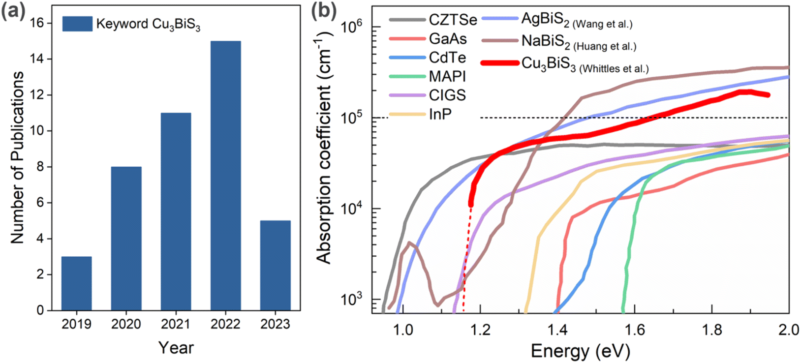 | ||
| Fig. 1 (a) Number of publications on Cu3BiS3-related papers in the period 2019 to 2023 (source: Scopus; keyword: Cu3BiS3, assessed on 02 June 2023). (b) Optical absorption coefficient of Bi-based chalcogenide materials. References inserted from Wang et al.,13 Huang et al.,14 and Whittles et al.15 | ||
CBS is a stable phase with a low melting point (∼527 °C), demonstrating the feasibility for grain growth at a low temperature.11 CBS exhibits remarkable optoelectronic properties such as a strong absorption coefficient (α > 105 cm−1) in the visible region (>1.6 eV), p-type conductivity, and an energy band gap value of ∼1.10–1.86 eV12 in the optimum range for different applications. Accordingly, bismuth-based chalcogenides have emerged as promising light absorbers with high optical absorption coefficient; namely AgBiS2 and NaBiS2. Fig. 1b shows the optical absorption coefficient of established semiconducting light absorbing materials. The optical absorption of CBS shows a steep increase close to the band edge, similar to halide perovskites and NaBiS2, and further increases >105 cm−1 above 1.7 eV, which is presumed to be the direct band edge of CBS.13–15 Moreover, it also indicates the peculiar high optical absorption behavior of Bi-based chalcogenide absorbers, which requires further attention.
The absorption coefficient together with the refractive index can be used to estimate the absorber layer thickness required for a given absorptance using the relation shown in eqn (1).
| a = (1 + [4n2αd]−1)−1, (in the presence of light scattering) | (1) |
Although the above-mentioned properties make CBS a promising candidate for PV and PEC application, they are not necessarily sufficient to achieve a superior performance. Indeed, CBS-based solar cells have demonstrated a power conversion efficiency of only 1.7%, which is far from its Shockley–Queisser limit (∼32.9% efficiency, 1.4 eV).17,18 Alternatively, the impressive solar-to-hydrogen (STH) conversion efficiency of 2.04% has been reported for a CBS photocathode-based PEC device, demonstrating excellent prospects for photoelectrocatalysis.19 Recently, Moon et al.20 achieved a solar-to-hydrogen efficiency of 2.33% under unassisted conditions using a Bi2S3–Cu3BiS3 mixed phase interlayer. The results displayed a high onset potential of 0.9 V (vs. RHE) and three-times higher photocurrent density (7.8 mA cm−2, at 0 V vs. RHE) compared to the single-phase Cu3BiS3-photocathode. Besides, the photocathode showed great stability for over 20 h. Notably, there is no report on photoelectrochemical CO2 reduction to date. This highlights the need to understand the property-performance gap in CBS compounds. Accordingly, more research is needed to enhance the functionality and versatility of the CBS photoabsorber, which can be achieved by understanding its optoelectronic properties by combining theoretical and experimental results. In this review, we employ a concerted and integrated theoretical and experimental approach to present an overall assessment of CBS compounds and their underlying challenges.
This review consists of three sections, as follows: (i) discussion on the crystallographic phase and electronic properties, (ii) synthetic methods (thin films and nanostructure), and (iii) assessment of photovoltaic and photo(electro)catalysis devices. Finally, a summary and outlook are presented.
2 Crystallographic structure and electronic properties of CBS with particular interest in solar energy conversion
2.1 Crystal structure and phase boundaries
The ternary copper chalcogenide system of CuxBiySz (CBS) is comprised of various phases, where among them, Cu3BiS3 is the most interesting, but still lacks extensive investigation. Historically, wittichenite was discovered in the early 19th century, but only artificially synthesized in 1947.21 The first fundamental work regarding the characterization of the crystal structure of wittichenite was published by Kocman and Nuffield.22 CBS crystallizes in an orthorhombic structure with the crystal symmetry belonging to the P212121 space group, which differs from the traditional cubic and hexagonal structures of the most important semiconductors.23 The details regarding its crystal structure parameters are shown in Table 1. All the lattice constants presented are experimental values and are in good agreement with other experimental and theoretical studies.24–27| Material | ||
|---|---|---|
| Parameter | CBS | |
| Crystal structure | Orthorhombic | |
| Space group | P212121 | |
| Lattice constant | a (Å) | 7.723 |
| b (Å) | 10.395 | |
| c (Å) | 6.716 | |
| ∝ = β = γ = 90° | ||
Fig. 2a depicts the crystal structure of wittichenite. Although Bi is trivalent in the CBS structure, similar to In and Ga in CIGS, it presents a distorted lattice. CBS shows a distorted tetrahedral structure with BiS3 units. In this structure, the Bi atom is located at one vertex of the tetrahedron and is bonded with three sulfur atoms. The Cu atom also has three-fold coordination to sulfur, which forms a trigonal distorted structure near the planar CuS3 unit. This distortion is due to the presence of a post-transition-metal cation (Bi3+) with an ns2 electronic configuration.28 Considering the Gillespie–Nyholm symmetry theory, also known as the valence-shell electron-pair repulsion (VSEPR) rule, s2 induces the distortion due to the presence of Bi 6s2 lone pairs, which causes the distortion of the crystal structure based on the interaction of empty states with the antibonding orbitals, resulting in an asymmetric electron density.
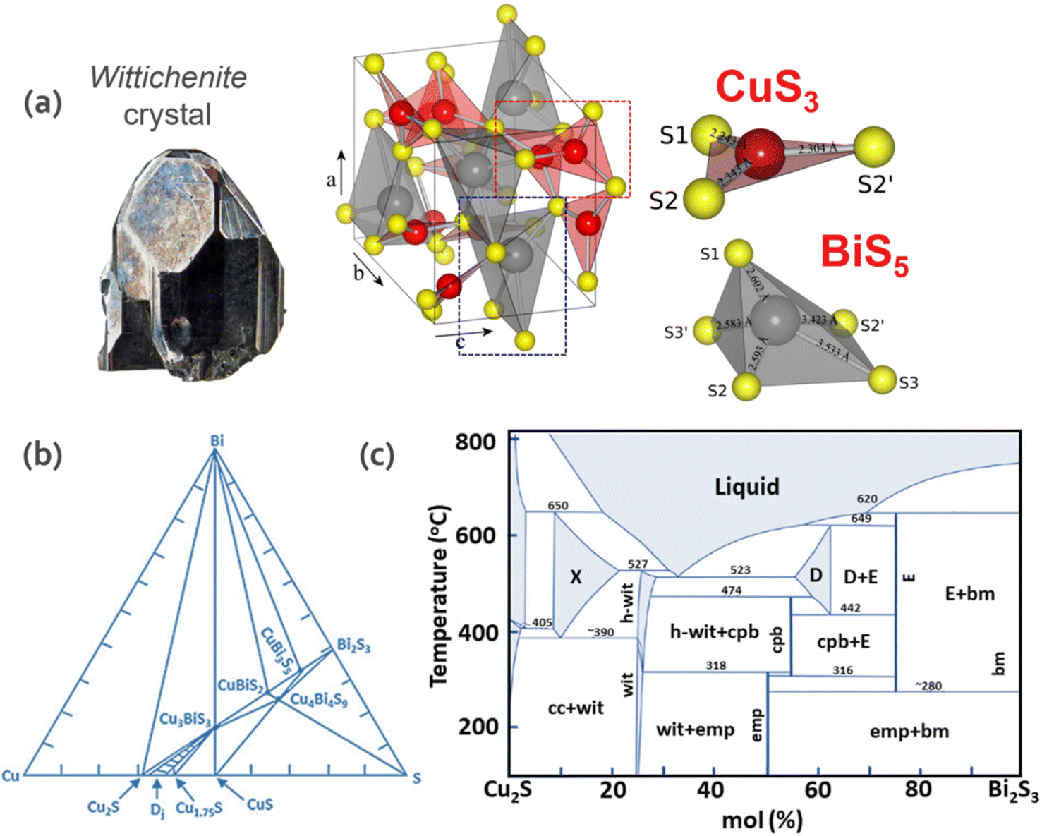 | ||
| Fig. 2 (a) Orthorhombic crystal structure of wittichenite (CBS), trigonal planar CuS3 unit showing distances between Cu (red) and S (yellow) atoms and distorted square pyramidal BiS5 unit showing distances between Bi (grey) and S (yellow) atoms. Adapted with permission from ref. 31 Copyright 2012 Elsevier B.V. (b) Triangle phase diagram of the Cu–Bi–S system at 300 °C. Adapted from the thesis of Chamorro et al.32 (c) Binary phase diagram of the Cu2S–Bi2S3 system. wit = CBS, h-wit = high form CBS, emp = emplectite, cpb = Cu4Bi7S12, X = Cu9BiS6, D = Cu3Bi5S9, E = CuBi3S5 cc = Cu2S, and bm = Bi2S3.33 | ||
The pseudo binary phase diagram of the Cu2S–Bi2S3 system and ternary phase diagram of the Cu–Bi–S system are depicted in Fig. 2b and c, respectively. To understand the phase transformation of the Cu–Bi–S system, they are discussed in terms of composition and temperature. In the CBS system, stoichiometric changes result in synthetic compounds with different phases. Among them, the Cu2S (chalcocite), Cu3BiS3 (wittichenite), Cu4Bi7S12 (cuprobismutite), CuBiS2 (emplectite) and Bi2S3 (bismuthinite) compounds are found in nature, while the Cu9BiS6, Cu3Bi5S9 and CuBi3S5 compounds have not been found to date. The former two present thermal stability in the range of 390–650 °C and 442–620 °C, respectively (Sugaki & Shima, 1972). Regarding the latter, CuBi3S5, to date there is no theoretical report and only one experimental report related to the synthesis of this phase29 showing n-type behavior with a carrier concentration and band gap of 3.75 × 10⁻¹⁷ cm−3 and 0.77 eV, respectively. CuBi3S5 exists as a stable and pure phase in the temperature range of 280–649 °C and it is expected to gain more attention in the future. CBS is thermally stable in the range of 350–527 °C, while CuBiS2 presents thermal stability below 317 °C, while at higher temperatures, it decomposes to wittichenite, covellite (CuS) and cuprobismutite, as shown in the reaction in eqn (2), demonstrating the challenge to obtain this phase.30 Consequently, while CuBiS2 is only stable at T < 319 °C, cuprobismutite is synthesized at higher temperatures.
| 8CuBiS2 ↔ Cu4Bi7S12 + Cu3BiS3 + CuS | (2) |
Although the compounds present in the Cu–Bi–S system are stable in a very narrow range, they exhibit interesting optoelectronic properties and show great potential to be applied in various energy systems. Therefore, further studies are needed to controllably synthesize and characterize these distinct observed phases. Regarding this, more information will be described in the following sections.
2.2 Electronic structure and optoelectronic properties: character of band edges, optical absorption, effective masses, and bandgaps
The electronic structure of CBS is governed by the fundamental differences in the chemical bonding between Cu, Bi and S in CuxBiySz compounds. The bonding and antibonding hybrid states form the conduction band minimum (CBM) and the valence band maximum (VBM), respectively. The antibonding character is formed by the interaction of the active ns2 lone pairs. This electronic structure is unusual compared to other semiconductor materials (bonding VBM and antibonding CBM). For this type of semiconductor, the electronic energy levels of an element are in resonance with the band edges. Accordingly, the removal or insertion of an element in the crystal structure leads to the formation of shallow states close to the band edges instead of deep defect states in the gap (i.e., trap centers, which restrict the charge transport). For this reason, the semiconductors containing antibonding states at the top of the valence band are also classified as defect tolerant.34 This implies that defect-tolerant semiconductors are insensitive to the presence of crystallographic defects (i.e., vacancies, interstitials) and have the capability to maintain their optoelectronic properties. Fig. 3a shows the orbital contributions from the individual atoms forming the electronic density of states for CuS, Bi2S3 and Cu3BiS3 compounds. In the case of CuS, the valence band maximum (VBM) and the conduction band minimum (CBM) consist of Cu d and S p states and Cu s with S p states, respectively.35 While for Bi2S3, the VBM and CBM are derived from Bi s with S p states and Bi p with S p states, respectively.36,37 Interestingly, in CBS, which contains contributions from both Cu and Bi, its VBM results from the coupling of the Cu d and S p states and its CBM is characterized by Bi p and S p states.15,25 According to the density of states (DOS) of CBS, as shown in Fig. 3b, it is possible to observe that the predominant contribution to the valence band comes from the Cu d orbital with some S p contribution. In CBS, the Bi s orbitals are fully occupied; hence, the empty Bi p orbitals are free to hybridize with the S p orbitals, forming the conduction band.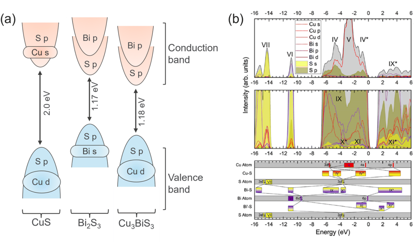 | ||
| Fig. 3 (a) Illustration of the main orbitals and their occupancy in the valence and conduction band for CuS, Bi2S3 and CBS. Blue and red colors correspond to occupied orbitals in VB and CB, respectively. (b) Density of states (DOS) curves for CBS material. Adapted with permission from ref. 15 Copyright 2019, the American Chemical Society. The top part shows the total and partial electronic DoS curves, where the black curve with gray shading is the total summed DoS. The middle part presents the zoomed region showing the underlying orbitals. The bottom part is the configuration energy (CE) for the valence orbitals, containing the bonding hybridizations. | ||
High optical absorption is a characteristic trait of CBS. The origin of its high optical absorption is related to the peculiar nature of its electronic bands. The optical absorption is governed by the transition matrix (VB|Ĥ|CB) and joint density of states (JDOS) at a given photon energy, which are related by Fermi's Golden rule, as shown in eqn (3):38
 | (3) |
Perovskites show excellent absorption characteristics owing to their direct band gap and p → p transition. The less dispersive p character of the perovskite CB, unlike the s-like more dispersive CB of CIS and CdTe, favors a high absorption coefficient.39 Thus, the p–p transition is highly desirable to achieve efficient optical absorption, which is possible for compounds having cations with a lone pair of s electrons,40e.g., the Pb2+ lone pair in perovskite. Interestingly, in the case of CBS, its optical transition is dominated by the p–p transition from the S p to Bi p states, which may be responsible for its high absorption. The presence of the Bi 6s2 lone pair promotes the p character of the VB similar to perovskite. Fig. 4 shows the density of states and corresponding schematic optical absorption from several materials including MAPbI3, CuInSe2, CdTe, and Cu3BiS3. As shown in Fig. 4d, it is clear that the VB of CBS resembles that of CIS, while its CB shows similar character to the perovskite CB. This makes it ideal for efficient optical transition, explaining the excellent absorption coefficient of CBS. The optical absorption of CBS originates from the dipole transition between the Cu-d/S-p orbitals (with a small contribution from the Bi s state due to the presence of the lone pair mechanism)15 of the VBM states and Bi-p/S-p of the CBM states. It is worth noting that a strong spin–orbit coupling (SOC) is expected in CBS due to the presence of the heavy Bi. However, the presence of SOC and its impact on the optical absorption of CBS are unknown.
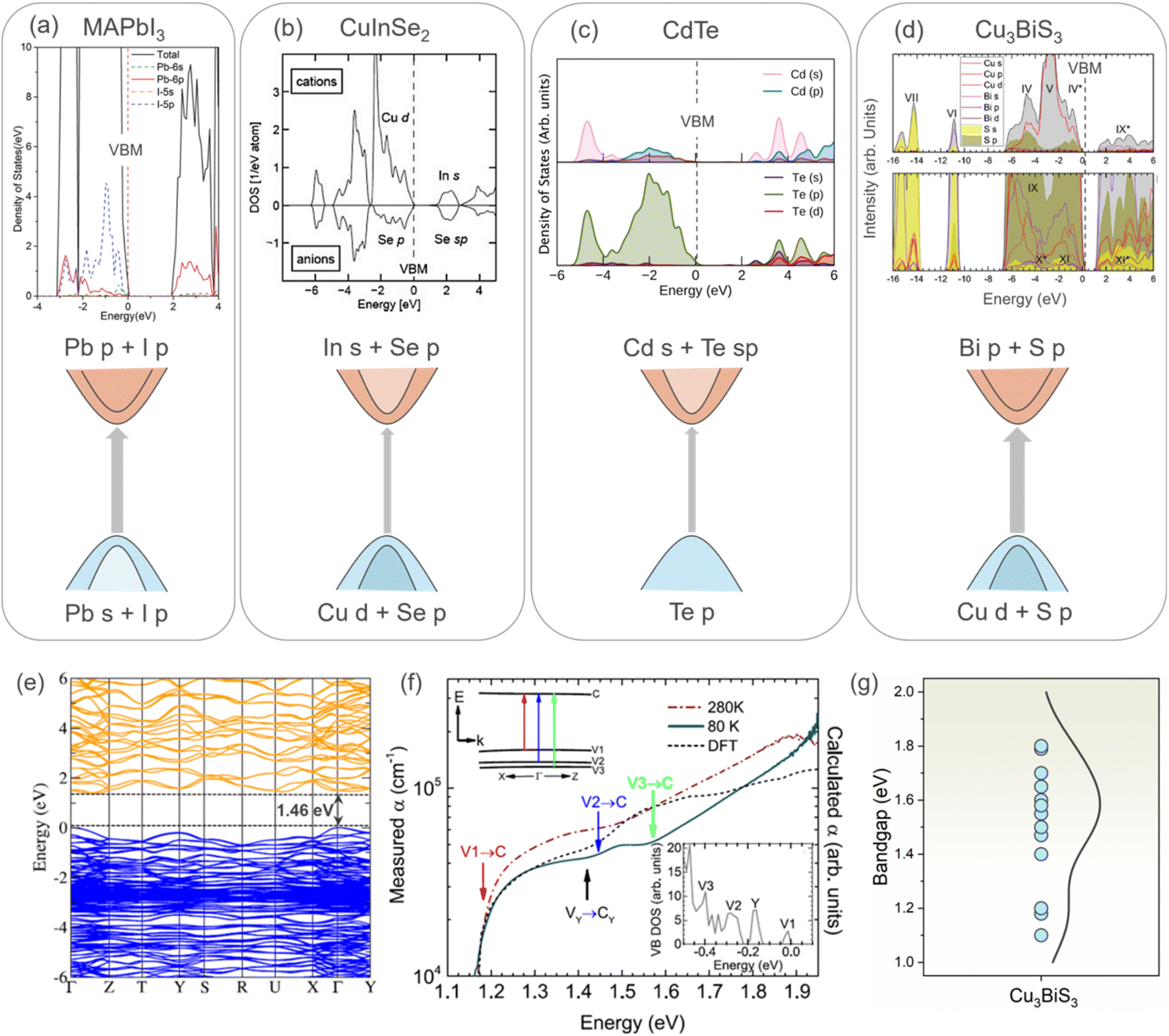 | ||
| Fig. 4 Density of states (DOS) and corresponding schematic of the optical absorption for (a) perovskite (MAPbI3). Reproduced with permission from ref. 61 Copyright 2019, The Royal Society of Chemistry. (b) Chalcopyrite CuInSe2. Reproduced with permission from ref. 62 Copyright 2010, John Wiley & Sons, Ltd. (c) CdTe. Reproduced under the terms of the CC-BY-4.0 license from ref. 63 Copyright 2021, the American Chemical Society. (d) Cu3BiS3.15 The dashed line indicates the valence band (zero energy). The grey arrow indicates the strength of the optical absorption. (e) Calculated electronic band structure for CBS using HSE06 + SOC DFT, VB and CB, as depicted in blue and orange, respectively. VBM is set as a reference in both cases. Figures (b), (c), and (d) reproduced with permission from ref. 15 Copyright 2019, the American Chemical Society. (f) Temperature-dependent optical absorption spectra of CBS (at 80 and 280 K, dark red and green lines, respectively). Inserted figure corresponds to DFT DoS at the top of the VB.15 (g) Bandgap energy values reported for CBS in the literature.15,26,45,53,57,58,60,64–67 | ||
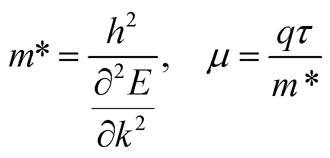
Fig. 4e shows the band structure of CBS, which was calculated using HSE06 + spin–orbit coupling (SOC). Both the VBM and CBM are located at the Γ point of the Brillouin zone for CBS. For most copper-based chalcogenide materials, such as CBS, s–p or p–d hybridization is present. The effective mass  carriers are related to the curvature of the individual bands. Thus, strongly curved wide bands (VBM and CBM more dispersive) suggest a lower effective mass, and hence higher carrier mobility.41 Also, the overlapping orbitals on neighboring atoms promotes larger delocalization, which leads to extended states/band, favoring the transport of free charge carriers and resulting in higher carrier mobility (specially desirable for photoabsorbers with an indirect bandgap).
The carrier mobility (μ) of a given material is related to the width and intrinsic dispersion of its conduction and valence bands. Eqn (4) describes the relationship between μ and effective mass (m*). In the case of n-type (or p-type) conductivity, m* is the electron effective mass  (or hole effective mass
  ). Both the carrier concentrations and mobilities can be determined from electrical Hall and thermoelectric measurements. Regarding
  there are only a few reports on CBS in the literature, and it was not discussed in detail, where
  was estimated to be 0.35 by Hall-voltage and thermoelectric Seebeck-coefficient measurements.42,43 Besides, the effective mass can play a crucial role in the net photo-current, and hence the cell efficiency for different applications (PV or PEC).44
 | (4) |
Table 2 shows the carrier concentration and carrier mobility values for CBS materials prepared by different synthesis methods. Most of the reports indicate p-type conductivity, similar carrier concentration (106–107 cm−3) and low carrier mobility (0.4–4.0 cm2 V−1 s−1), except for the study by Li et al.,45 Fazal et al.,46 and Lee et al.47 A low carrier mobility indicates the active role of electronic defects in the material. Defects are known to act as recombination centers and affect the carrier transport in different ways through the scattering process within the grain interior and/or at the grain boundaries (GB).48 It is known that the grain boundaries can be regulated by changing the synthesis method and minimizing the transport barriers, limiting the conductivity of the film.42 The fact that low mobility values are obtained regardless of the synthesis route (solution or vacuum processed) indicates the intrinsic nature of the defects in CBS. Although most of the studies report that the presence of defects has a negative impact on the electronic properties of materials, defect engineering can be an optimal approach for some specific applications, specifically photoelectrocatalysis.49–51
| Ref. | Chemistry | Composition/synthesis method | Carrier type | Carrier concentration (cm−3) | Carrier mobility (cm2 V−1 s−1) |
|---|---|---|---|---|---|
| 27 | Solution processing | CBS/CuO and Bi2S3 dissolved in thiol-amine and dried at 400 °C | p-type (Hall measurements) | 4.2 × 10¹⁷ | 0.4 |
| 42 | Vapor phase synthesis | CBS/Co-evaporation of Cu, Bi, and S onto a substrate at 300 °C | p-type (Hall measurements) | 2.00 × 10¹⁶ | 4.00 |
| 45 | Solution processing | CBS/DMSO*-based solution processed, short-time drying of spin-coated precursor film | p-type (Hall measurements) | 5.65 × 10¹⁶ | 52.83 |
| 46 | Chemical bath deposition | CBS/deposited for 12 h | p-type (four-probe method) | 6.07 × 10¹⁶ | 34.90 |
| 57 | Solution processing | CBS/Spin-coating Cu and Bi oxides followed by sulfurization | p-type (Hall measurements) | 5.10 × 10¹⁶ | 3.73 |
| 58 | Vapor phase synthesis | CBS/co-evaporation precursors followed by annealing process | p-type (Hall measurements) | 2.80 × 10¹⁶ | 1.50 |
| 59 | Vapor phase synthesis | CBS/one-stage co-evaporation process | p-type (Hall measurements) | 7.48 × 10¹⁶ | 3.95 |
| 60 | Solution processing | CBS/spin coating precursor solution, followed by annealing on a hotplate | p-type (Hall measurements) | 6.39 × 10¹⁷ | 3.09 |
| 47 | Solution processing | CBS/chemical bath deposition technique | p-type (Hall measurements) | 2.57 × 10¹⁶ | 71.20 |
The fundamental bandgap energy (Eg) is established as the energetic difference between the VBM and CBM. Upon illumination, the photogenerated charge carriers at the CBM relax to the VBM through radiative transitions in direct bandgap semiconductors. In contrast, for indirect bandgap semiconductors, the absorbed light is emitted as a nonradiative transition via phonons, thus losing its energy. The bandgap of CBS is under debate in the literature due to the ill-defined nature of its band edges and possibly the presence of defect states, emphasizing the necessity for further investigations. In the literature, there is a spread in the experimental value of the reported data (1.0–1.8 eV), showing a direct bandgap for CBS. In contrast, theoretical studies predict an indirect band gap for CBS. Fig. 4g shows both the experimental and theoretical band gap energy values reported for CBS. Notably, a significant difference is observed in the value of the bandgap, which may be due to the synthesis method (hence defect) adopted. Most of the studies rely on optical absorption spectroscopy to determine the bandgap. The variation in the bandgap value may originate from the measurement itself given that it is difficult to unambiguously ascertain the bandgap for indirect semiconductors from their absorption onset alone. In the case of a small energy difference between the direct and indirect band edge and/or the presence of defect states near the band edge, the bandgap appears to be pseudo-direct. Additionally, this variation can be due to the crystallinity of the material or the crystal orientation. For instance, a single crystal exhibits a lower band gap compared to thin films.52
For materials targeted for application in solar conversion, i.e., as semiconductors or photovoltaics, strong optical absorption is crucial. CuxBiySz shows an ideal photo absorption in the visible wavelength region with an optimal absorption coefficient (>105 cm−1) compared to other Cu–S-based materials, such as CIGS and CZTS. However, according to the band structure (Fig. 4e), from the Γ and X points of the Brillouin zone, it is observed that the low density of states (DoS) reduces the absorption extent of the CBS material. The fundamental bandgap energy for CBS is 1.372 eV and indirect;15 however, its absorption is dominated by photon absorption with higher energy direct transitions of >1.4 eV (V2 → C, inset in Fig. 4e) due to the large contribution given by the presence of density of states at the valence band maximum.
Besides, to measure the bandgap, very thin films of CBS are currently being used in several experimental studies. In the case of indirect bandgap materials, a large thickness is required to realize the complete absorption of the incident light, which can also be another reason for the huge disparity among the reported results.
Unfortunately, the methods used to measure the band gap energy are not suitable to determine its nature given that it gets non-trivial due to the presence of many peaks close to the VB. Thus, other techniques must be explored to reliably determine the bandgap such as photoluminescence (PL), photothermal deflection spectroscopy (PDS), and quantum efficiency measurements. There are very few studies reporting a measurable PL for CBS,53–56 given that the PL quantum yield of the material is expected to be quite low due to its indirect bandgap or presence of deep defects, which is highly likely in this compound. Considering the above-mentioned arguments, the defect tolerance of CBS has to be scrutinized and more studies are required to understand the nature of its intrinsic defects.
2.3 Energy band alignment
The other essential criteria for the optoelectronic properties of materials towards device applications are the energetic band edges offsets and Fermi level (EF) (i.e., ionization potential, work function, and electron affinity). In a device, its interface/junction determines the transport of charge carriers (electrons and holes). Therefore, it is important to have both materials energetically aligned for efficient charge transfer. For most CBS studies reported in the literature, CdS (n-type) is commonly used as an n-type buffer layer to form a heterojunction, given that it shows great results for CIGS and CZTS. However, as shown in Fig. 5a, the energy band positions of CdS are not properly aligned with respect to CBS. Thus, it can be inferred that the low solar cell efficiencies observed in CBS devices are due to the lack of understanding of the above-mentioned issue and the improper choice of n-type layer. Similarly, hole-selective layers should also be investigated. Fig. 5b illustrates an ideal band alignment scheme for the CBS material.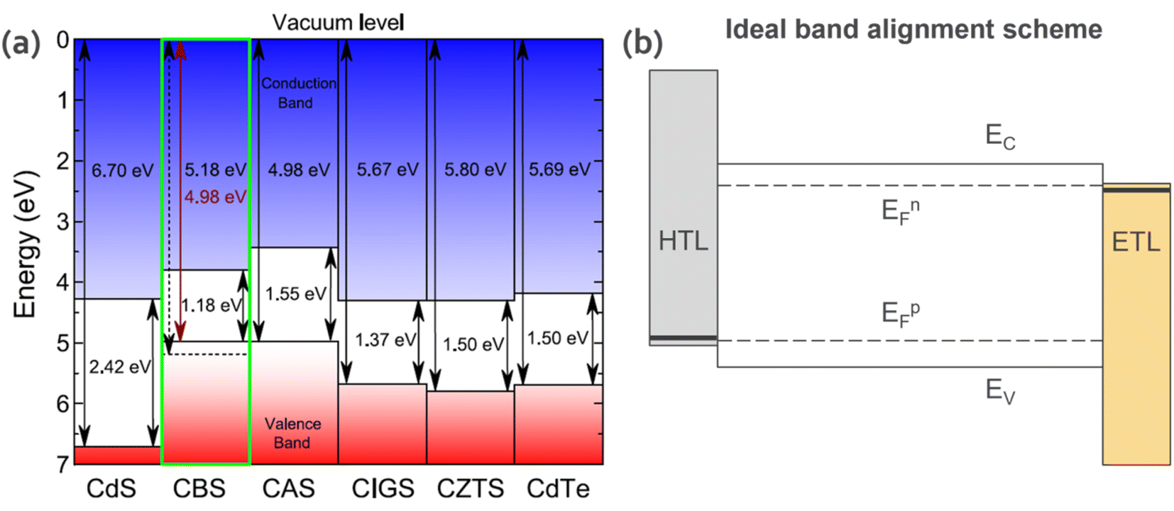 | ||
| Fig. 5 (a) Vacuum-aligned band diagram between CBS and other common absorber layers. Reproduced with permission from ref. 15 Copyright 2019, the American Chemical Society. (b) Ideal band alignment scheme for CBS. HTL = hole transport layer; ETL = electron transport layer; EFp = Fermi energy level for p-type material; EFn = Fermi energy level for n-type material; EC = conduction band energy level; and EV = valence band energy level. | ||
3 Synthesis methods
3.1 Nanocrystals
The synthesis of Cu–Bi–S nanocrystals is challenging due to the high level of difficulty in controlling their growth and their features, such as size, shape, and configuration. In colloidal synthesis, specific parameters (i.e., nucleation and growth kinetics) lead to the formation of uniform nanocrystals. This is done by optimizing the material preparation conditions and the type of capping ligands used.The first report on the synthesis of CBS nanocrystals by Yan et al.68 employed a hot-injection method based on colloidal synthesis using copper(II) acetylacetonate, bismuth(III) nitrate pentahydrate [atomic ratio Cu:Bi = 3] and oleylamine (OLA) ligand. High-quality CBS nanocrystals showed good crystallinity and an average particle size in the range of 8–11 nm. Bi2S3 and CuS phases were identified as key intermediate steps to form CBS NCs and the shape of the nanocrystal could be tuned by varying the precursor concentration and reaction temperature. Besides, the optical bandgap of the CBS nanocrystal (1.56 eV) was found to be larger than that of the CBS bulk (1.40 eV) due to the quantum confinement effect. Also, the CBS nanocrystals showed a good photo response, signifying their potential to be used as a thin film for solar energy conversion.
In another study, Chakraborty et al.65 obtained pure CBS semiconducting nanoflowers (450–500 nm) and nanospheres (6–9 nm) using a facile hot injection method. The precursors, reaction temperature and ligand type play a key role in dictating the morphology and the proposed reaction mechanism is shown in Fig. 6a. Specifically, 1-DDT (dodecanethiol) is the determinant in the formation of CBS nanoflowers, given that it leads to particle agglomeration, which is favorable for the growth of nanoflowers. The photo-response from CBS nanoflowers showed a prominent current under illumination compared to nanospheres, further demonstrating the potential of nanocrystals in optoelectronic devices.
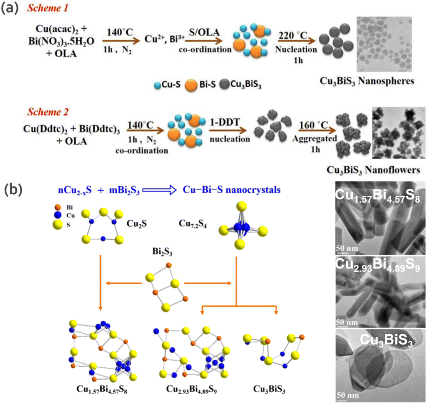 | ||
| Fig. 6 (a) Schematic mechanism of the growth and optimum conditions for obtaining CBS nanosphere and nanoflower-shaped NCs. Reproduced with permission from ref. 65 Copyright 2019, Elsevier B.V. (b) Composition and phase-controlled synthesis scheme of CBS nanocrystals synthesized by Cu2−xS with Bi2S3 of different ratios. Reproduced with permission from ref. 69 Copyright 2018, Wiley-VCH Verlag GmbH & Co. KGaA, Weinheim. | ||
Although CBS is the most studied compound in the Cu–Bi–S phase, other phases have also gained interest with particular focus on Bi-rich phases. Ren et al.69 fabricated three Cu–Bi–S nanocrystal phases (Cu1.57Bi4.57S8, Cu2.93Bi4.89S9 and CBS), in which the structure and bandgap of two phases (they were only discovered as a mineral) were reported for the first time. Cu–Bi–S phase formation proceeds through the following reaction: aCu2−xS + bBi2S3 → cCu–Bi–S NCs. This is due to the fact that Bi3+ is very sensitive to the redox environment in the reaction (i.e., presence of ligands DDT or OAm) and copper has affinity towards sulfur, which leads to the reduction of Bi3+ to the zerovalent state.70 Thus, to address this limitation, the Bi–S chemical bond was stabilized, as illustrated in Fig. 6b. In the proposed scheme, CBS was obtained from Bi2S3 precursor containing different amounts and types of Cu2−xS (Cu2S or Cu7.2S4) reactants in DDT. To obtain Cu1.57Bi4.57S8 and Cu2.93Bi4.89S9 compounds, Cu2S and Cu7.2S4 were used as precursors, respectively. For the initial Cu:Bi ratio of 2:1, CBS nanoplates were obtained. Cu1.57Bi4.57S8 and Cu2.93Bi4.89S9 showed a nanorod morphology and direct band gap of 1.12 and 1.27 eV, respectively, while CBS showed a polygonal nanoplate morphology and band gap of 1.64 eV.
Deshmukh and collaborators71 studied the formation of flower-like CBS with nanoflakes formed on glass substrates via the chemical bath deposition technique, using CuCl2·2H2O, Bi(NO3)3·5H2O, and CH4N2S as the precursors and hexamethylenetetramine (HMT) as the complexing agent. This process is based on the slow release of Cu2+, Bi3+, and S2− ions in the precursor solution, which forms CBS when these ions exceed the solubility product of CBS. The nanoflowers presented a diameter of 1052 nm (using the Debye–Scherrer formula). The as-prepared CBS showed a bandgap of 1.57 eV; however, after annealing treatment, a direct bandgap of 1.42 was obtained. The decrease in the bandgap was attributed to the phase transformation from an amorphous to polycrystalline structure.
3.2 Thin film
The synthesis of CuxBiySz thin films has been well explored in the literature, and hence a variety of techniques have been reported. Mesa and Gordillo16 prepared CBS thin films via a two-step co-evaporation process. The first step involved the formation of a BixSy layer by the co-evaporation of Bi and S elements (substrate temperature of 300 °C). Subsequently, Cu was evaporated in the second step to convert BixSy to CBS (at around 300 °C). The results showed a high optical absorption (>104 cm−1) and bandgap of 1.41 eV. In the study by Hu et al.,72 CBS thin films were prepared via low-temperature (100–150 °C) hydrothermal (HD) synthesis using copper and bismuth-based compounds and thiourea (Tu). The material consisted of whisker-like particles. The best-quality CBS was obtained at the growth temperature of 120 °C for <8 h. Better homogeneity was realized by liquid-solution diffusion due to the formation of [Cu(Tu)x]+ and [Bi(Tu)y]3+ complexes, which reduced the dissociation of ions, and thus inhibited the formation of secondary phases (Cu2S and Bi2S3) in the solution.In another study by Koskela et al.,27 thiol-amine (1,2-ethanedithiol, EDT) was used to dissolve CuO and Bi2S3 precursors to form a colloidal ink (yellowish) for the preparation of CBS. The ink was solution-processed on a fluorine-doped tin oxide (FTO) substrate and annealed at 400 °C under N2 to form a pure-phase CBS film (Fig. 7a). The as-produced film exhibited a high absorption coefficient (α = 5 × 104 cm−1) and optical absorption bandgap of 1.47 eV, as shown in the inverse logarithmic derivative (ILD) plot in Fig. 7b. Besides, the resistivity of CBS follows typical semiconducting characteristics with temperature, as shown in Fig. 7c.
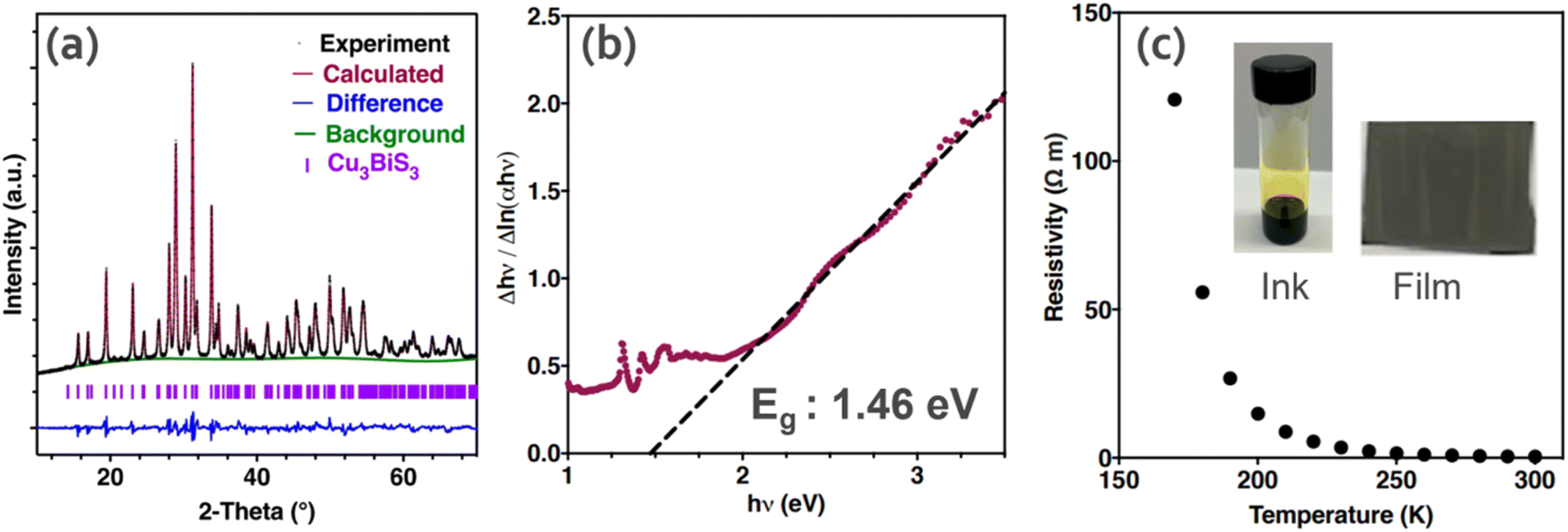 | ||
| Fig. 7 (a) X-ray diffraction pattern for pure-phase Cu3BiS3. (b) Inverse logarithmic derivative plot from absorption spectra derived from transmittance. The dashed black line corresponds to the linear regression used to estimate the optical band gap. (c) Resistivity versus temperature for CBS synthesized by solution processing. (Inserted) picture of semiconductor ink containing CuO and Bi2S3 dissolved and Cu3BiS3 thin film. Reproduced with permission from ref. 27 Copyright 2021, the American Chemical Society. | ||
Chen et al.73 prepared an Au–In2S3/CBS thin film heterostructure using a combination of simple spray pyrolysis deposition (SPD) on molybdenum-coated glass (Mo-SLG) and chemical bath deposition. Firstly, a CBS precursor solution was prepared using a simple solution of Cu(NO3)2·3H2O (99.9%) and Bi(NO3)3·5H2O (99.9%) in HNO3. Then, the precursor was sprayed (controlled at 7 min) on an Mo/SLG substrate (reaction controlled at 380 °C). After this step, the precursor film was sulfurized in a tube furnace at 550 °C for 1 h. The In2S3 layer was prepared via the chemical bath deposition method, using InCl3, thioacetamide and acetic acid in water. The bath was heated at 65 °C for 30 min, followed by annealing at 100 °C for 20 min to obtain In2S3/CBS. Mott–Schottky analysis confirmed the p-type semiconductor characteristics. The band gap was calculated to be 1.58 eV.
Fazal et al.46 reported the preparation of a CBS thin film by the complexation of Cu2+ and Bi3+ ions with EDTA to form [Cu(EDTA)]−2 and [Bi(EDTA)]−1. Then, the S2− ions released from thioacetamide reacted with Bi3+, accompanied by a change in the color of the solution to grayish brown, indicating the successful synthesis of CBS by ion consumption and integration into the Bi2S3 lattice. The slower kinetics posed a major limitation in obtaining a thicker film. This issue was solved by increasing the deposition time from 6 to 12 h. The proposed reaction mechanism is shown in eqn (5) and (6).
 | (5) |
 | (6) |
The spray pyrolysis technique is very attractive to produce thin films given that it is a versatile method that enables facile control of the thickness. CBS was successfully deposited on a glass substrate using BiCl3, CuCl2 and thiourea precursor solutions74 with varying substrate temperatures in the range of 250–400 °C. The optical bandgap was estimated to be 1.72 and 1.65 eV for the films synthesized at 250 °C to 300 °C, and 350 °C to 400 °C, respectively. All the thin-films showed p-type conductivity. In another approach, spray pyrolysis was performed using bismuth tris(4-methylbenzodithioate) [Bi(4-MBDT)3] mixed with copper(I) acetate and 1,2-ethanedithiol precursors.75 In this work, CBS was synthesized on a glass substrate maintained at 150 °C ≤ Tdep ≥ 200 °C (at higher temperatures, unknown phases appeared, and at lower temperatures, the complete conversion of the precursor to CBS was not obtained). This technique allowed the formation of films with an easily controlled and reproducible thickness. The optimum condition to spray the precursor solution was identified to be 175–200 °C with 12 deposition cycles. The authors observed a broad light absorption up to 1000 nm. However, it was not possible to determine the bandgap of the material due to the unclear absorption onset energy. Attempts to fabricate a functioning photovoltaic device remain unsuccessful. The authors highlighted the necessity to identify suitable hole-transporting materials for CBS.
The choice of synthesis method depends on the desired properties of the material being synthesized. Table 3 shows the correlation between some targeted properties (particle, compositional, thickness control, and uniformity) and the synthesis method that could be more suitable to achieve it.
| Synthesis Method | Type | Composition and phase control | Particle size control | Scalability | Suitable for | Comment |
|---|---|---|---|---|---|---|
| Hot injection | NCs |

|

|

|
PEC | Limited yield |
| Chemical bath deposition | TF |

|

|

|
PV, PEC | Slower growth kinetics, crystallinity control is difficult |
| Hydrothermal synthesis | NCs |

|

|

|
PEC | Considerations required for substrate |
| Spray pyrolysis | TF |

|

|

|
PV, PEC | Less control overgrowth kinetics |
| Co-evaporation | TF |

|

|

|
PV, PEC | High throughput is a challenge |
4 Applications
4.1 Thin-film photovoltaic device
Thin-film photovoltaics (PV) is excellent technology with a thinner light absorber layer, which makes it lighter, flexible and reduces the material consumption. The potential of CBS material in the field of solar PV was only recognized in 1997.76 There are promising findings on the structural, morphology, synthesis, and optoelectronic properties of the CBS material; however, its extension to the device level is still sporadic, with limited architectures explored in the literature.Yin and Jia et al.77 successfully fabricated CBS nanosheet films (30 nm thick) on TiO2 nanorod arrays on FTO substrate via the solvothermal route, forming a p–n heterojunction. The photoelectric properties of the CBS/TiO2 composite film exhibit a fill factor of 60.8%, Jsc of 4.449 mA cm−2, Voc of 442 mV and energy conversion efficiency of 1.281%, which is 2.5-times higher than the TiO2 standalone device. The reported energy conversion efficiency of the CBS/TiO2 thin-film solar cell is very promising.
Li et al.45 reported a facile and low-toxic solution route for the deposition of CBS films without post sulfurization. They also proposed a prototype glass/Mo/CBS/CdS/ZnO/ITO/Al solar cell. This device showed a short-circuit current density (Jsc) of 2.37 mA cm−2, open-circuit voltage (Voc) of 0.19 V, fill factor (FF) of 37.56% and conversion efficiency of 0.17% (Fig. 8a and b). The authors mentioned that the low Jsc may be due to the poor collection of photogenerated charges carriers, which is probably limited by the improper junction between CBS and CdS (more information can be found in the report by Whittles et al.15).
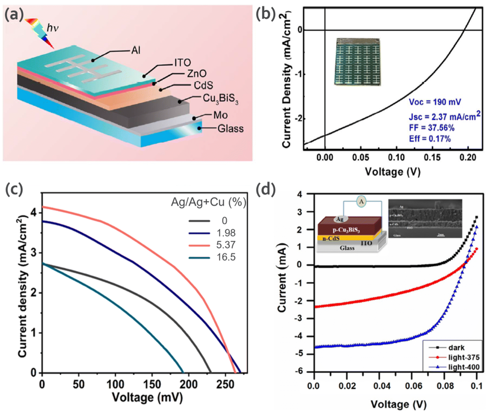 | ||
| Fig. 8 (a) Schematic diagram of the CBS solar cell device. (b) J–V curve of the CBS solar cell under AM 1.5G simulated irradiation. The inset shows an image of the fabricated device. Reproduced with permission from ref. 45 Copyright 2017, Elsevier B.V. (c) J–V curves for different Ag/(Ag + Cu) ratio values. Reproduced with permission from ref. 60 Copyright 2021, Elsevier Ltd (d) Typical I–V curves for the CBS thin film solar cell device at 375 °C and 400 °C obtained under illumination of 100 mW cm−2. The inserted figure shows a schematic diagram and cross-sectional SEM image of the device. Reproduced with permission from ref. 59 Copyright 2019, Elsevier B.V. | ||
Yang et al.58 studied the effect of the atomic ratio of the Cu/Bi precursors (1.0–3.0) and the annealing temperature in the range of 350 °C to 475 °C for CBS thin films prepared via the co-evaporation of bismuth and CuS materials in a vacuum system, followed by an annealing process. In this work, the samples annealed at 450 °C showed better results. The Cu/Bi atomic ratio of 1.5 showed improved mobility and carrier density (1.5 cm2 V−1 s−1 and 2.8 × 1016 cm−3, respectively). The CBS thin film showed a high absorption coefficient of 1.5 × 105 cm−1 at 600 nm. The device structure of Glass/Mo/CBS/CdS/ZnO/ZnO:Al/Ni/Al yielded a Voc of 0.32 V and FF of 18.2 mA cm−2 with 1.7% power conversion efficiency, which is the highest performance reported to date.
Zhao and collaborators60 studied the impact of Ag doping on CBS, aiming to optimize the material properties for photovoltaic applications. The CBS-Ag absorber layer was prepared by solution processing. To control the Ag concentration in individual precursor solutions, the mole ratio of Ag/(Ag + Cu) was varied to be 0%, 1.98%, 5.37%, 16.5% and 35.8%, which was denoted as A0, A1, A2, A3 and A4, respectively. The devices were fabricated based on the structure of SLG/Mo/CBS/CdS/ZnO/ITO/Al. Fig. 8c shows the illuminated current density–voltage (J–V) curves for the A0–A3 samples. The sample with 5.37% Ag/(Ag + Cu) showed a Voc of 263 mV, Jsc of 4.15 mA cm−2 and FF of 44.1%. A power energy conversion of 0.48% was obtained. Compared to A0 (no doping), an improvement of ∼85% by 5.37% Ag doping was clearly evident.
In another study by Hussain et al.,59 CBS thin films were deposited on a soda-lime glass substrate via a one-stage co-evaporation process using Cu2S and Bi2S3 sources at different deposition temperatures (room temperature and in the range of 275–400 °C). The crystalline quality of the films increased with an increase in the deposition temperature. The CBS films were applied in solar cell structures (glass/ITO/n-CdS/p-CBS/Al). Fig. 8d shows the performance of the CBS thin film solar cell devices deposited at 375 °C and 400 °C. The results showed photovoltaic behavior and an increase in the photocurrent from 1.0 to 3.0 mA under illumination at 0.09 V. To date, CBS has shown a relatively poor solar cell performance with a maximum of 1.7%, which is way far from the Shockley–Queisser limit (∼33.7% efficiency, 1.3 eV).17 The theoretical device simulation study by Mesa et al.78 showed a Voc of 0.712 V, Jsc of 36.25 mA cm−2, FF of 79.54% and efficiency of 19.86%, which are quite far from the experimental studies.
Thus, the performance-limiting factors of CBS devices need to be identified. The role of intrinsic defects in carrier recombination and energy band alignment requires attention to realize the potential of CBS-based devices we believe that this material continues to generate interest and more exploration is required in this front.
4.2 Photoelectrocatalysis
Photoelectrocatalysis (PEC) has been used in many different applications such as disinfection, degradation of contaminant compounds, CO2 reduction, and water splitting. Typically, a p-type semiconductor is used as a photocathode to drive photoelectrochemical reactions. Briefly, when a p-type semiconductor is immersed in an electrolyte, charge transfer occurs due to the chemical potential equilibrium (Fermi level, EF) of the semiconductor and the redox potential of the electrolyte. This process results in an electric field, manifested by band bending (downward for p-type) of the semiconductor, as shown in the scheme presented in Fig. 9. Upon illumination, the excited electrons are driven towards the interface due to the gradient of the quasi–Fermi levels, where they can reduce the different redox species at the surface, such as water or CO2, to hydrogen or hydrocarbons. Simultaneously, the other half reaction is balanced by the oxidation reaction at the anode (counter electrode). The photovoltage required to drive the electrochemical reaction can be achieved either by a single material with the optimum bandgap or tandem systems (i.e., heterojunction and Z-scheme). Readers are encouraged to refer to Walter et al.79 for a focused discussion on photoelectrochemistry.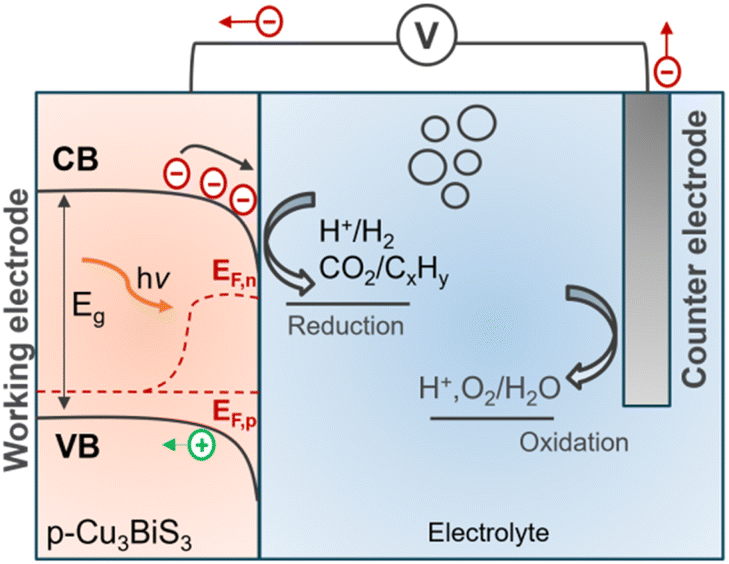 | ||
| Fig. 9 Schematic of the PEC setup showing the band bending and quasi–Fermi levels for electrons (EF,n) and holes (EF,p) for a typical p-type semiconductor. | ||
Cu–Bi–S compounds have not been well investigated as photocatalysts although they present outstanding optoelectronic properties. There are few reports on water splitting and/or hydrogen evolution reaction employing CBS. Kamimura and collaborators80 fabricated CBS on a molybdenum-coated glass substrate employing a simple electrodeposition method using Cu(NO3)2·3H2O and Bi(NO3)3·5H2O as precursors. An n-type buffer layer, In2S3, was deposited by chemical bath atop CBS films, followed by the deposition of Pt on In2S3/CBS films to improve the photocatalytic response given that Pt nanoparticles present a low overpotential. A band gap of 1.63 eV and shift in the onset potential towards a positive potential were observed for the Pt–In2S3/CBS material compared to Pt-CBS. However, the applied potential necessary for PEC hydrogen evolution was +0.55 (∼+0.6 V) vs. RHE in 0.1 M Na2SO4 (pH 6) aqueous solution. At a higher potential, the film suffered from degradation, which was ascribed to the self-reduction and/or reduction of the In2S3 buffer layer. The faradaic efficiency of 90% was maintained after 60 min of light illumination.
Li et al.81 reported the fabrication of a CBS nanorod/TiO2 (C@T) heterojunction (Fig. 10a) via a solution dip-coating method. To analyze the photo-response of CBS nanorods/C@T towards water-splitting potential, PEC measurements were performed under illumination for 10 s. The device showed a higher photocurrent response (∼10−4 A cm−2) for the C@T heterojunction compared to bare CBS nanorods (Fig. 10b). The improvement was due to the formation of a heterojunction, which enhanced the separation and transfer of photogenerated charge carriers, decreased the recombination, and consequently increased the photocurrent.
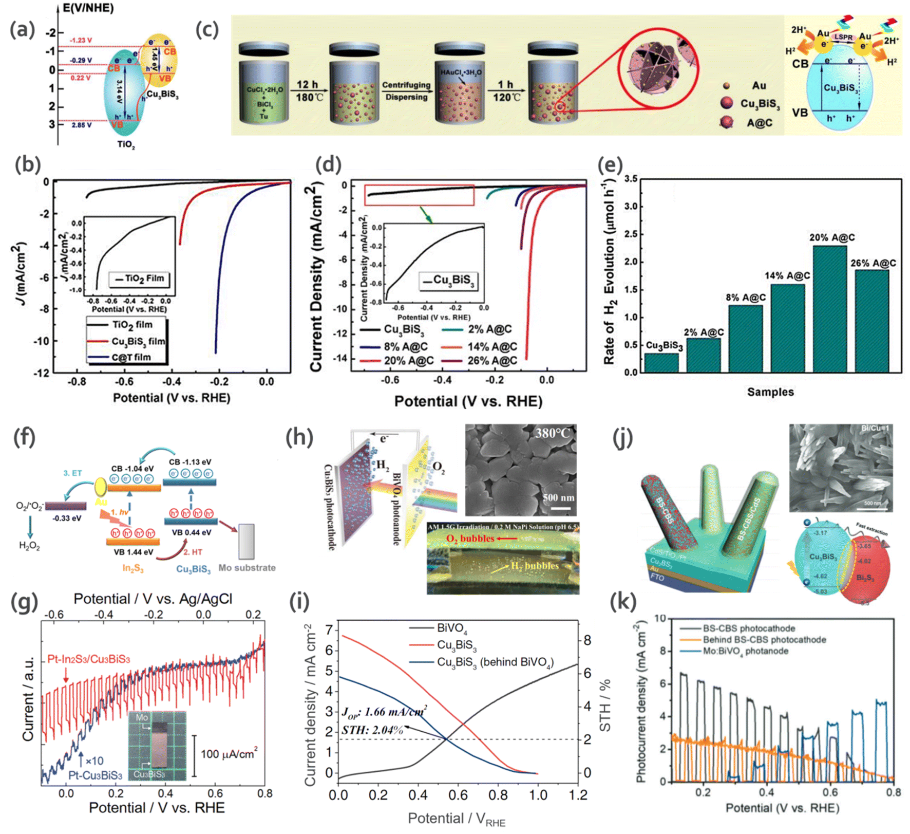 | ||
| Fig. 10 (a) Schematic illustration of the band diagram of TiO2 and CBS heterojunction towards carrier separation and transfer process. (b) LSV polarization curves for TiO2, CBS nanorods and C@T heterojunction. (Inset) Magnified polarization curves for TiO2. Reproduced with permission from ref. 81 Copyright 2018, The Royal Society of Chemistry. (c) Schematic illustration of the fabrication of flower-like CBS and A@C composite. (d) LSV polarization curves of CBS and A@C samples. (Inset): magnified polarization curves for CBS. (e) Rate of H2 production by photoelectrocatalysis for CBS and A@C (Au/CBS) samples with different mass ratios. Reproduced with permission from ref. 87 Copyright 2021, The Royal Society of Chemistry. (f) Energy diagram for Au–In2S3/CBS electrodes depicting the process of H2O2 formation. (g) Current–potential curves for Pt-CBS3 and Pt–In2S3/CBS. Na2SO4 solution (pH 6) was used as the electrolyte, under chopped illumination from AM 1.5 G solar simulator. (Inset): picture of the fabricated Cu3BiS3 material. Reproduced with permission from ref. 73 Copyright 2022, Elsevier B.V. (h) SEM of CBS film sprayed on substrate at the temperature of 380 °C, and working diagram of CBS-BiVO4 tandem cell. (i) J–V curves for CBS photocathode, BiVO4 photoanode and CBS photocathode behind the BiVO4 photoanode. (Inset: Jop = operation point photocurrent density and STH = solar to hydrogen efficiency). Reproduced under the terms of the CC-BY-4.0 license from ref. 19 (j) Schematic for BS/CBS (Bi2S3/CBS) photocathode and band diagram calculated from UPS. (k) Photocurrent density versus potential for BS-CBS photocathode, BiVO4 photoanode, and BS-CBS photocathode behind the BiVO4 photoanode. Reproduced under the terms of the CC-BY license from ref. 20. | ||
In another study by Li et al.,45 they investigated the HER. They fabricated flower-like CBS using a Cu and Bi-based solution mixed with Tu. Nanocomposites of Au-CBS (A@C) were also prepared via the direct growth of Au NPs on the surface of CBS via a one-step solvothermal method (Fig. 10c). Pure CBS presented inactive photoelectrocatalytic behavior (0.35 μmol h−1 of H2), as shown in Fig. 10d. In contrast, all the A@C composites exhibited enhanced catalytic activity for H2 evolution with an increasing load of Au NPs (Fig. 10e) due to their higher contact area and active sites. Besides, the difference in work function between CBS and Au and higher conductivity of Au accelerated the separation of photogenerated charges.
Recently, Chen and collaborators73 fabricated a uniform polycrystalline Au/In2S3/CBS thin film via spray pyrolysis (more details of the synthesis presented in Section 3.2) for the generation of hydrogen peroxide (H2O2). Fig. 10f shows the energy band diagram for the studied material. The selectivity for O2 and H2O2 photoelectrochemical formation improved due to the presence of Au nanoparticles, where 5.5 mg L−1 h−1 cm−1 of H2O2 was produced with a Faraday efficiency of 71%. To the best of our knowledge, this is the first time that CBS was used to produce H2O2, which shows its versatility for different photoelectrochemical applications. The current–voltage curves for Pt–Cu3BiS3 and Pt–In2S3/Cu3BiS3 are shown in Fig. 10g.
In a recent study by Huang et al.,82 they fabricated CBS employing one-step spray pyrolysis and tested it for the PEC hydrogen evolution reaction (HER). The influence of the substrate temperature (360–420 °C) and Cu:Bi molar ratio (1:1, 2:1, 4:1 and 5:1) in the precursor solution was investigated. Among them, the Cu:Bi molar ratio of 3:1 matched well with the reference pattern for CBS without showing secondary phases, while the other Cu:Bi ratios presented secondary phases (Cu2−xS and Cu3Bi3S7). The 3:1 Cu:Bi thin-film at 380 °C showed better photocatalytic behavior upon further coating with CdS, TiO2 and Pt nanoparticles. The device was coupled to a BiVO4 photoanode to build a tandem cell (CBS-BiVO4). For this device, they achieved high stability (over 60 h) and STH efficiency (2.04%) for the bias-free standalone system. An illustration of the cell and the J–V curves of the materials are presented in Fig. 10h and I, respectively.
The presence of mixed phases can result in structural instability, which can lead to a loss in the photocatalytic activity and overall performance. However, recently, in a report by Moon et al.,20 it was shown that mixed phases can actually allow better band alignment with the n-type layer (band diagram showing the relative energy positions of each of the semiconductors is shown in Fig. 10j). This changes the band structure of the material, which leads to an improvement in charge transport. The Bi2S3–Cu3BiS3 (BS-CBS) mixed phase with elongated 1D nanorods achieved a high onset potential of 0.9 V and showed three-times higher performance compared to the single-phase CBS. Thus, the BS-CBS internal heterojunction facilitated charge separation. A standalone PEC–PEC tandem device was proposed by coupling the BS-CBS photocathode with a BiVO4-based photoanode. Fig. 10k shows the J–V curves for BS-CBS, Mo:BiVO4, and BS-CBS photocathode behind the BiVO4 photoanode. The BS-CBS-based tandem cell showed an efficiency of 2.33% and stability of over 21 h.
The photo(electro)reduction of CO2 using CBS has not been demonstrated to date. The first work on CO2 reduction using photo electrocatalysis was reported by Halmann et al.,83 in which CO2 was converted to methanol, formic acid and formaldehyde by a GaP electrode. Since then, various studies have been proposed. The complex dependence among the reaction products and intermediates, supporting electrolyte, applied potential, pH gradient, and reaction kinetics is not well understood. Besides, in the CO2RR, losses are caused by band bending (kinetic), resistance (electrolyte) and the overvoltage potential, and therefore an energy input of higher than 1.7 eV is necessary to overcome this limitation. In this case, a material presenting a bandgap of >1.8–2.0 eV is required for CO2 photo electroreduction application, and therefore CBS is a potential candidate for CO2 reduction, given that it fulfills most of the above-mentioned criteria. However, the low photovoltage and aqueous stability of CBS require detailed studies in this front. It is well known that copper-based materials suffer from photo corrosion (photo instability). For instance, copper oxide suffers from redox instabilities and photodegradation due to the oxidation/reduction of Cu+ (Cu2O) to form Cu2+ (CuO) or Cu0, respectively.84–86 There are many strategies to overcome this limitation, which includes the creation of a p–n heterojunction to avoid the recombination of photogenerated charge carriers and multifunctional coatings to protect the surface and improve the long-term durability.
5 Future perspectives
Bi-based chalcogenides have attracted significant attention, presenting interesting optoelectronic properties and multifunctionalities, which make them suitable for application in solar cells and PECs. We observed that while the low Voc of CBS-based photocathodes in solar cells is a major limitation, their show an excellent photoelectrochemical performance with a high onset potential. The defect tolerance from the electronic configuration needs to be experimentally scrutinized. Although antibonding VBM states generally lead to shallow defect levels in the band gap for specific point defects (e.g., Cu vacancy in CuInSe2 forms a shallow acceptor level due to the antibonding p-d states), it is paramount to consider all the possible point defects to examine the recombination centers or traps, given that some of them can act as recombination centers or carrier traps. Deep defects have been observed in Cu3N (interstitial defect Cui) and CIGSe(S)2 (antisite (In,Ga)Cu) semiconductors despite having a defect tolerant electronic configuration.88–90 Addressing the Voc deficit in CBS requires an in-depth understanding of the factors responsible for the Voc losses, as follows: (i) phase purity and doping control, (ii) identification of deep defects, (iii) determination of carrier lifetime and mobility limiting mechanism, (iv) role of intrinsic disorder and band tails, and (v) knowledge of energy band positions to construct heterojunctions with minimized interface recombination.Here, we provide possible solutions towards the development of CBS.
(i) Phase purity and stoichiometric control: although many reports claim the synthesis of phase-pure CBS based on XRD analysis, it is possible that a low concentration of impurity phases may be excluded in the traditional XRD measurements. In this case, the more sensitive Raman spectroscopy will be useful to rule out the presence of secondary phases. Moreover, the complex carbon-containing precursors in the commonly used solution processing and relatively low processing temperatures can lead to nanoscale amorphous phase impurities, which remain undetected in XRD and Raman measurements. Accordingly, high-resolution transmission electron microscopy and sensitive magnetic measurements will be useful to identify these defects and amorphous phase domains. It is worth investigating single crystals and vacuum processed polycrystalline thin films to make a comparative study on the inevitability of certain defects and phase impurities in CBS.
(ii) Open questions on intrinsic properties and defects: the fundamental properties such as the electronic band structure, nature of the optical bandgap, charge carrier diffusion lengths (carrier mobility and lifetimes), doping, intrinsic defects and their respective energies in the bandgap are not well understood. The lack of control of the electronic properties explains the poor performance of photovoltaic devices. It is important to establish whether the carrier mobilities are limited by phonon scattering or impurity scattering. A recent study reported a low carrier lifetime of 0.7 ns, indicating high recombination losses.20 This clearly suggests the active role of deep defects in the material.
Theoretical studies will be highly useful to gain insights into the optoelectronic properties of CBS and validate experimental conclusions. For instance, experimental results show direct bandgap behavior for CBS, while theoretical calculations predict indirect behavior. Thus, this discrepancy needs to be addressed. Furthermore, the role of deep defects and their importance is still lacking. Atomic-level insights into defects can be obtained by advanced characterization techniques such as scanning transmission microscopy (STM) and X-ray photoelectron spectroscopy (XPS). STM allows the direct visualization of lattice defects and XPS enables the measurement of the chemical and electronic states of the elements. Spectroscopic techniques such as photoluminescence and femtosecond transient spectroscopy will be useful to analyze the performance-limiting deep defects and carrier dynamics in CBS. The knowledge of performance-limiting defects is necessary to engineer high-performing devices and develop passivation strategies.
(iii) Improving the optoelectronic properties and charge transport: control of the doping and morphology is critical to improve the optoelectronic properties. An effective doping strategy may be guided by leveraging the knowledge of doping in common chalcogenide absorbers (CIGS and CZTS). Varying the growth conditions from Cu-poor (Bi-rich) to Cu-rich (Bi-poor), cation substitution with Ag/Na, anion substitution with oxygen/selenium, and alkali doping are promising routes in this regard. Besides doping, control of the morphology is desirable for specific applications. It is worth emphasizing that the impurity phases, which are otherwise considered detrimental, may have better optical and electrical properties than wittichenite CBS itself. Thus, the controllable synthesis of different phases may open new avenues for the Cu–Bi–S phase. The knowledge of energy band alignment with common ETL and HTL contact layers is essential to enhance the charge carrier transport and maximize the carrier extraction efficiency. The application of the conventionally used buffer layers, such as CdS, may not be suitable in terms of band alignment. In this case, alternative buffer layers such as Zn(O,S), In2S3, and (Zn,Sn)O may be interesting to explore. Besides the buffer layers, the band offsets can also be changed by tuning the energy band of CBS by alloying and/or cation/anion substitution. However, explicit observation via experimental measurement for tuning the band edge energies of CBS is lacking to date.
(iv) Interface-engineered device architectures: there are few reports on CBS photovoltaic devices, and most of them show a low efficiency. Thus, more studies on high-quality and defect-passivated CBS absorbers91 are required. More device architectures need to be explored to assess the full potential of CBS. Fig. 11 shows the feasible device architectures.
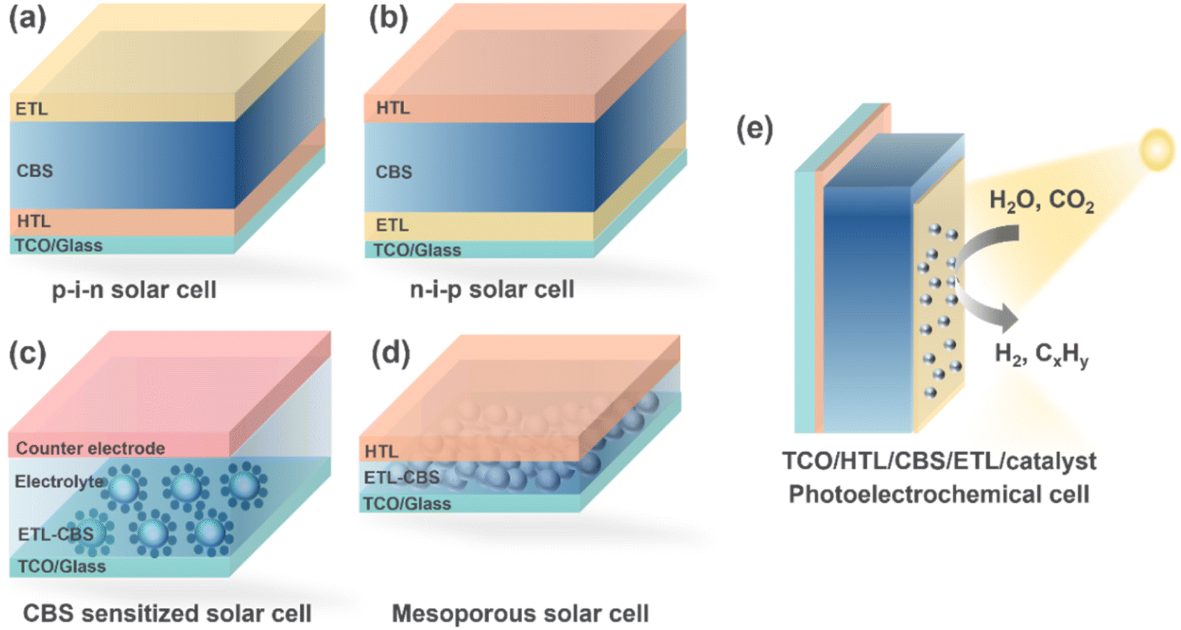 | ||
| Fig. 11 CBS device architecture engineering for (a) p-i-n solar cell, (b) n-i-p solar cell, (c) CBS-sensitized solar cell, (d) mesoporous solar cell and (e) photoelectrochemical cell. ETL = electron transport layer; HTL = hole transport layer; and TCO = transparent conductive oxide. | ||
(v) Long-term stability: the stability of the photocathode is a major concern in photoelectrochemical applications, which may be due to the environment (oxidation) and aqueous medium (redox instability). Additionally, photoinduced degradation (photocorrosion) is also a major cause of the degradation of many photocathodes, such as Cu2O. A protection barrier is required to prevent the degradation in PC and PEC devices. Laminating the surface with hybrid polymeric encapsulants embedded with catalysts provides higher operational stability. Atomic layer deposition (ALD) is also an option to suppress corrosion or add functionality to the device (i.e., MoS2 exhibits intrinsic catalytic activity). Finally, the construction of heterostructures or Z-schemes can also be an alternative to enhance the stability for (photo)electrocatalytic reactions.
6 Concluding remarks
In summary, the CuxBiySz system remains unexplored, requiring further studies on this front. In particular, the Cu3BiS3 compound exhibits excellent optical absorption characteristics and suitable bandgap for solar cell and photoelectrochemical applications. CBS offers new opportunities for both domains. Although photovoltage limitations have hampered the development of CBS-based solar cells, promising results on photoelectrochemical water splitting have opened new avenues. More complex photoelectrochemical reactions, such as CO2 reduction can be targeted with modified interfaces and surfaces. Nevertheless, fundamental studies with innovative device designs are required to fully harness the potential of the CBS absorber. The development of an effective and stable visible light active photocatalyst is crucial to achieve high efficiency in (photo)electrochemical reactions.Author contributions
Daniely S. and Sudhanshu S.: conceptualization, writing – original draft. Sudhanshu S. and Bart V.: reviewing and editing, supervision. Bart V.: funding acquisition.Conflicts of interest
There are no conflicts to declare.Acknowledgements
The authors acknowledge Catalisti VLAIO (Vlaanderen Agentschap Innoveren & Ondernemen) for their funding through the Moonshot SYN-CAT project (HBC.2020.2614). SS acknowledges funding from the European Union's Horizon Europe program under the Marie Skłodowska-Curie Grant Agreement No. 101067667.References
- NREL, Best Research-Cell Efficiency Chart, https://www.nrel.gov/pv/cell-efficiency.html, accessed 20-07-2022.
- B. Zohuri and P. McDaniel, in Introduction to Energy Essentials, ed. B. Zohuri and P. McDaniel, Academic Press, 2021, pp. 255–276 Search PubMed.
- S. Ikeda, High Temp. Mater. Processes, 2021, 40, 446–460 CrossRef CAS.
- A. Redinger, D. M. Berg, P. J. Dale and S. Siebentritt, J. Am. Chem. Soc., 2011, 133, 3320–3323 CrossRef CAS PubMed.
- T. Tanaka, T. Sueishi, K. Saito, Q. Guo, M. Nishio, K. M. Yu and W. Walukiewicz, J. Appl. Phys., 2012, 111, 053522 CrossRef.
- E. Deady, C. Moon, K. Moore, K. M. Goodenough and R. K. Shail, Ore Geol. Rev., 2022, 143, 104722 CrossRef.
- R. Mohan, Nat. Chem., 2010, 2, 336 CrossRef CAS PubMed.
- U. S. G. Survey, Bismuth. Mineral Commodity Summaries, 2021 Search PubMed.
- U. S. G. Survey, Bismuth Mineral Commodity Summaries, 2014 Search PubMed.
- 5NPlus, 2019 Annual Report, 2019 Search PubMed.
- Y. Fang, W. Zhao, W. Li and X. Han, Appl. Phys. A, 2021, 127, 9 CrossRef CAS.
- S. G. Deshmukh and V. Kheraj, Nanotechnol. Environ. Eng., 2017, 2, 15 CrossRef.
- Y. Wang, S. R. Kavanagh, I. Burgués-Ceballos, A. Walsh, D. O. Scanlon and G. Konstantatos, Nat. Photonics, 2022, 16, 235–241 CrossRef CAS.
- Y.-T. Huang, S. R. Kavanagh, M. Righetto, M. Rusu, I. Levine, T. Unold, S. J. Zelewski, A. J. Sneyd, K. Zhang, L. Dai, A. J. Britton, J. Ye, J. Julin, M. Napari, Z. Zhang, J. Xiao, M. Laitinen, L. Torrente-Murciano, S. D. Stranks, A. Rao, L. M. Herz, D. O. Scanlon, A. Walsh and R. L. Z. Hoye, Nat. Commun., 2022, 13, 4960 CrossRef CAS PubMed.
- T. J. Whittles, T. D. Veal, C. N. Savory, P. J. Yates, P. A. E. Murgatroyd, J. T. Gibbon, M. Birkett, R. J. Potter, J. D. Major, K. Durose, D. O. Scanlon and V. R. Dhanak, ACS Appl. Mater. Interfaces, 2019, 11, 27033–27047 CrossRef CAS PubMed.
- F. Mesa and G. Gordillo, J. Phys.: Conf. Ser., 2009, 167, 012019 CrossRef.
- W. Shockley and H. J. Queisser, J. Appl. Phys., 1961, 32, 510–519 CrossRef CAS.
- S. Rühle, Sol. Energy, 2016, 130, 139–147 CrossRef.
- D. Huang, L. Li, K. Wang, Y. Li, K. Feng and F. Jiang, Nat. Commun., 2021, 12, 3795 CrossRef CAS PubMed.
- S. Moon, J. Park, H. Lee, J. W. Yang, J. Yun, Y. S. Park, J. Lee, H. Im, H. W. Jang, W. Yang and J. Moon, Adv. Sci., 2023, 10, 2206286 CrossRef CAS PubMed.
- E. W. Nuffield, Econ. Geol., 1947, 42, 147–160 CrossRef CAS.
- V. Kocman and E. W. Nuffield, Acta Crystallogr., Sect. B: Struct. Crystallogr. Cryst. Chem., 1973, 29, 2528–2535 CrossRef CAS.
- K. W. Böer and U. W. Pohl, in Semicond. Phys., ed. K. W. Böer and U. W. Pohl, Springer International Publishing, Cham, 2018, vol. 3, pp. 59–108 Search PubMed.
- J. Capistrán-Martínez, D. Loeza-Díaz, D. Mora-Herrera, F. Pérez-Rodríguez and M. Pal, J. Alloys Compd., 2021, 867, 159156 CrossRef.
- M. Kumar and C. Persson, J. Renewable Sustainable Energy, 2013, 5, 031616 CrossRef.
- A. B. Kehoe, D. J. Temple, G. W. Watson and D. O. Scanlon, Phys. Chem. Chem. Phys., 2013, 15, 15477–15484 RSC.
- K. M. Koskela, A. C. Tadle, K. Chen and R. L. Brutchey, ACS Appl. Energy Mater., 2021, 4, 11026–11031 CrossRef CAS.
- A. Walsh, D. J. Payne, R. G. Egdell and G. W. Watson, Chem. Soc. Rev., 2011, 40, 4455–4463 RSC.
- F. Miao, S. Wan, Q. Zhang, X. Lu, G. Gu and S. Yin, Chin. J. Quantum Electron., 2011, 28, 558 CAS.
- M. F. Razmara, C. M. B. Henderson, R. A. D. Pattrick, A. M. T. Bell and J. M. Charnock, Mineral. Mag., 1997, 61, 79–88 CrossRef CAS.
- D. Colombara, L. M. Peter, K. Hutchings, K. D. Rogers, S. Schäfer, J. T. R. Dufton and M. S. Islam, Thin Solid Films, 2012, 520, 5165–5171 CrossRef CAS.
- W. Chamorro, F. Mesa, M. Hurtado and G. Gordillo, Study of structural and morphological properties of ZnS films deposited on Cu3BiS3, in 25th European Photovoltaic Solar Energy Conference and Exhibition, Spain, 2010, pp. 575−579, DOI:10.4229/25thEUPVSEC2010-1DV.3.8.
- A. Kitakaze, Phase Relations of Some Sulfide Systems, Mem Fac Eng Yamaguchi Univ, 2017 Search PubMed.
- A. Zakutayev, C. M. Caskey, A. N. Fioretti, D. S. Ginley, J. Vidal, V. Stevanovic, E. Tea and S. Lany, J. Phys. Chem. Lett., 2014, 5, 1117–1125 CrossRef CAS PubMed.
- R. M. Córdova-Castro, M. Casavola, M. van Schilfgaarde, A. V. Krasavin, M. A. Green, D. Richards and A. V. Zayats, ACS Nano, 2019, 13, 6550–6560 CrossRef PubMed.
- H. Ben Abdallah and W. Ouerghui, Opt. Quantum Electron., 2021, 54, 20 CrossRef.
- R. S. Silva, H. D. Mikhail, E. V. Guimarães, E. R. Gonçalves, N. F. Cano and N. O. Dantas, Molecules, 2017, 22, 1142 CrossRef PubMed.
- C. Kittel, Introduction to Solid State Physics, Wiley, 2004 Search PubMed.
- J. Y. Kim, J.-W. Lee, H. S. Jung, H. Shin and N.-G. Park, Chem. Rev., 2020, 120, 7867–7918 CrossRef CAS PubMed.
- W.-J. Yin, T. Shi and Y. Yan, J. Phys. Chem. C, 2015, 119, 5253–5264 CrossRef CAS.
- R. v. d. Krol and M. Graetzel, Electronic Materials, Science & Technology, Photoelectrochemical Hydrogen Production, 2012 Search PubMed.
- F. Mesa, G. Gordillo, T. Dittrich, K. Ellmer, R. Baier and S. Sadewasser, Appl. Phys. Lett., 2010, 96, 082113 CrossRef.
- B. Murali, M. Madhuri and S. B. Krupanidhi, J. Appl. Phys., 2014, 115, 173109 CrossRef.
- B. B. Dumre, N. J. Szymanski, V. Adhikari, I. Khatri, D. Gall and S. V. Khare, Sol. Energy, 2019, 194, 742–750 CrossRef CAS.
- J. Li, X. Han, Y. Zhao, J. Li, M. Wang and C. Dong, Sol. Energy Mater. Sol. Cells, 2018, 174, 593–598 CrossRef CAS.
- T. Fazal, S. Iqbal, M. Shah, Q. Mahmood, B. Ismail, H. O. Alsaab, N. S. Awwad, H. A. Ibrahium and E. B. Elkaeed, Results Phys., 2022, 36, 105453 CrossRef.
- D. Lee, H. Ahn, S. Park, H. Shin and Y. Um, Nanosci. Nanotechnol. Lett., 2018, 10, 1–4 CrossRef CAS.
- A. M. Russell and K. L. Lee, in Structure-Property Relations in Nonferrous Metals, 2005, pp. 18–27 Search PubMed.
- T. Wei, Y.-N. Zhu, X. An, L.-M. Liu, X. Cao, H. Liu and J. Qu, ACS Catal., 2019, 9, 8346–8354 CrossRef CAS.
- D. Maarisetty and S. S. Baral, J. Mater. Chem. A, 2020, 8, 18560–18604 RSC.
- Z. Wang, M. Xiao, J. You, G. Liu and L. Wang, Acc. Mater. Res., 2022, 3, 1127–1136 CrossRef CAS.
- S. Trivedi, D. Prochowicz, N. Parikh, A. Mahapatra, M. K. Pandey, A. Kalam, M. M. Tavakoli and P. Yadav, ACS Omega, 2021, 6, 1030–1042 CrossRef CAS PubMed.
- J. Zhong, W. Xiang, Q. Cai and X. Liang, Mater. Lett., 2012, 70, 63–66 CrossRef CAS.
- M. V. Yakushev, P. Maiello, T. Raadik, M. J. Shaw, P. R. Edwards, J. Krustok, A. V. Mudryi, I. Forbes and R. W. Martin, Thin Solid Films, 2014, 562, 195–199 CrossRef CAS.
- O. C. Olatunde and D. C. Onwudiwe, Results Chem., 2022, 4, 100273 CrossRef CAS.
- Y. Pan, H. Deng, D. Zheng, J. Chen, Y. Zhong, J. Tao, P. Yang and J. Chu, J. Mater. Sci.: Mater. Electron., 2022, 33, 585–595 CrossRef CAS.
- L. Zhang, X. Jin, C. Yuan, G. Jiang, W. Liu and C. Zhu, Appl. Surf. Sci., 2016, 389, 858–864 CrossRef CAS.
- Y. Yang, X. Xiong, H. Yin, M. Zhao and J. Han, J. Mater. Sci.: Mater. Electron., 2019, 30, 1832–1837 CrossRef CAS.
- A. Hussain, J. T. Luo, P. Fan, G. Liang, Z. Su, R. Ahmed, N. Ali, Q. Wei, S. Muhammad, A. R. Chaudhry and Y. Q. Fu, Appl. Surf. Sci., 2020, 505, 144597 CrossRef CAS.
- W. Zhao, Y. Fang, W. Li and X. Han, Sol. Energy, 2021, 221, 109–113 CrossRef CAS.
- Y.-B. Lu, W.-Y. Cong, C. Guan, H. Sun, Y. Xin, K. Wang and S. Song, J. Mater. Chem. A, 2019, 7, 27469–27474 RSC.
- S. Siebentritt, M. Igalson, C. Persson and S. Lany, Prog. Photovoltaics, 2010, 18, 390–410 CAS.
- S. R. Kavanagh, A. Walsh and D. O. Scanlon, ACS Energy Lett., 2021, 6, 1392–1398 CrossRef CAS PubMed.
- S. U. Rahayu and M.-W. Lee, AIP Conf. Proc., 2020, 2221, 030005 CrossRef CAS.
- M. Chakraborty, R. Thangavel, P. Komninou, Z. Zhou and A. Gupta, J. Alloys Compd., 2019, 776, 142–148 CrossRef CAS.
- E. Verónica, M. T. S. Nair and P. K. Nair, Semicond. Sci. Technol., 2003, 18, 190 CrossRef.
- N. J. Gerein and J. A. Haber, Chem. Mater., 2006, 18, 6297–6302 CrossRef CAS.
- C. Yan, E. Gu, F. Liu, Y. Lai, J. Li and Y. Liu, Nanoscale, 2013, 5, 1789–1792 RSC.
- X. Ren, L. Yuan, Q. Liang, R. Xie, Z. Geng, Y. Sun, L. Wang, K. Huang, T. Wu and S. Feng, ChemPlusChem, 2018, 83, 812–818 CrossRef CAS PubMed.
- S.-K. Han, C. Gu, M. Gong and S.-H. Yu, J. Am. Chem. Soc., 2015, 137, 5390–5396 CrossRef CAS PubMed.
- S. G. Deshmukh, S. J. Patel, K. K. Patel, A. K. Panchal and V. Kheraj, J. Electron. Mater., 2017, 46, 5582–5588 CrossRef CAS.
- J. Hu, B. Deng, C. Wang, K. Tang and Y. Qian, Mater. Chem. Phys., 2003, 78, 650–654 CrossRef CAS.
- C. Chen, M. Yasugi, L. Yu, Z. Teng and T. Ohno, Appl. Catal., B, 2022, 307, 121152 CrossRef CAS.
- S. Liu, X. Wang, L. Nie, L. Chen and R. Yuan, Thin Solid Films, 2015, 585, 72–75 CrossRef CAS.
- N. Pai, J. Lu, D. C. Senevirathna, A. S. R. Chesman, T. Gengenbach, M. Chatti, U. Bach, P. C. Andrews, L. Spiccia, Y.-B. Cheng and A. N. Simonov, J. Mater. Chem. C, 2018, 6, 2483–2494 RSC.
- P. K. Nair, L. Huang, M. T. S. Nair, H. Hu, E. A. Meyers and R. A. Zingaro, J. Mater. Res., 1997, 12, 651–656 CrossRef CAS.
- J. Yin and J. Jia, CrystEngComm, 2014, 16, 2795–2801 RSC.
- F. Mesa and D. Fajardo, Can. J. Phys., 2014, 92, 892–895 CrossRef CAS.
- M. G. Walter, E. L. Warren, J. R. McKone, S. W. Boettcher, Q. Mi, E. A. Santori and N. S. Lewis, Chem. Rev., 2010, 110 Search PubMed.
- S. Kamimura, N. Beppu, Y. Sasaki, T. Tsubota and T. Ohno, J. Mater. Chem. A, 2017, 5, 10450–10456 RSC.
- J. Li, X. Han, M. Wang, Y. Zhao and C. Dong, New J. Chem., 2018, 42, 4114–4120 RSC.
- Y.-T. Huang, S. R. Kavanagh, D. O. Scanlon, A. Walsh and R. L. Z. Hoye, Nanotechnology, 2021, 32, 132004 CrossRef CAS PubMed.
- M. Halmann, Nature, 1978, 275, 115–116 CrossRef CAS.
- T. Baran, A. Visibile, M. Busch, X. He, S. Wojtyla, S. Rondinini, A. Minguzzi and A. Vertova, Molecules, 2021, 26, 7271 CrossRef CAS PubMed.
- S. Tiwari, S. Kumar and A. K. Ganguli, J. Photochem. Photobiol., A, 2022, 424, 113622 CrossRef CAS.
- Q. Peng, S. Zhang, H. Yang, B. Sheng, R. Xu, Q. Wang and Y. Yu, ACS Nano, 2020, 14, 6024–6033 CrossRef CAS PubMed.
- J. Li, Y. Zhao, X. Han and D. Xiao, New J. Chem., 2021, 45, 1231–1239 RSC.
- Y. S. Yee, H. Inoue, A. Hultqvist, D. Hanifi, A. Salleo, B. Magyari-Köpe, Y. Nishi, S. F. Bent and B. M. Clemens, Phys. Rev. B, 2018, 97, 245201 CrossRef CAS.
- Q. Cao, O. Gunawan, M. Copel, K. B. Reuter, S. J. Chey, V. R. Deline and D. B. Mitzi, Adv. Energy Mater., 2011, 1, 845–853 CrossRef CAS.
- S. Shukla, M. Sood, D. Adeleye, S. Peedle, G. Kusch, D. Dahliah, M. Melchiorre, G.-M. Rignanese, G. Hautier, R. Oliver and S. Siebentritt, Joule, 2021, 5, 1816–1831 CrossRef CAS.
- F. Mesa, A. Dussan, B. A. Paez-Sierra and H. Rodriguez-Hernandez, Univ. Sci., 2014, 19, 99–105 Search PubMed.
| This journal is © The Royal Society of Chemistry 2023 |