
InCl3-modified SnO2 as an electron transporting layer for Cd-free antimony selenide solar cells†
Lei
Huang‡
ab,
Junjie
Yang‡
ab,
Yujian
Xia‡
c,
Peng
Xiao
ab,
Huiling
Cai
ab,
Aoxing
Liu
ab,
Yan
Wang
ab,
Xiaosong
Liu
*c,
Rongfeng
Tang
 *ab,
Changfei
Zhu
ab and
Tao
Chen
*ab
*ab,
Changfei
Zhu
ab and
Tao
Chen
*ab
aHefei National Research Center for Physical Sciences at the Microscale, CAS Key Laboratory of Materials for Energy Conversion, School of Chemistry and Materials Science, University of Science and Technology of China, Hefei, Anhui 230026, China. E-mail: rftang@ustc.edu.cn; tchenmse@ustc.edu.cn
bInstitute of Energy, Hefei Comprehensive National Science Center, Hefei, China
cNational Synchrotron Radiation Laboratory (NSRL), University of Science and Technology of China, Hefei, Anhui 230029, China. E-mail: xsliu19@ustc.edu.cn
First published on 20th July 2023
Abstract
Solar cells based on Sb2Se3 have attracted increasing attention due to its excellent optoelectronic properties and low-cost fabrication. Up to now, high-efficiency Sb2Se3 solar cells with a superstrate structure have always used CdS as an electron transport layer (ETL). However, the parasitic absorption caused by CdS reduces the light absorption of the Sb2Se3 absorber layer, and combined with the toxicity of the Cd element, jointly causes its limitation in practical application. Tin oxide (SnO2) is a wide-bandgap ETL and has been widely used in solar cells due to its suitable energy level, high electron mobility, and good stability. However, Sb2Se3 films deposited on metal oxides always exhibit poor quality. In this study, we demonstrate a facile strategy to improve the quality of an Sb2Se3 film by modifying a SnO2 layer with InCl3. We find that InCl3 post-treatment can optimize the band alignment between SnO2 and Sb2Se3, improve the quality of the SnO2/Sb2Se3 heterojunction, and reduce deep-level defects. As a result, the PCE improves from 1.51% to 5.52%. Thus, this work offers a simple and effective way to improve the quality of Sb2Se3 films deposited on SnO2 ETLs and provides a new path towards fabricating Cd-free Sb2Se3 solar cells.
Introduction
Binary antimony selenide (Sb2Se3), consisting of earth-abundant and low-toxicity elements, is considered as a promising light-absorbing material due to its excellent optoelectronic properties, such as an ideal optical band gap (∼1.0–1.3 eV), a high light absorption coefficient (>105 cm−1 in the visible region) and decent carrier mobility (∼10 cm2 V−1 s−1).1 According to the Shockley–Queisser (S–Q) limit, the maximum power conversion efficiency (PCE) of an Sb2Se3 single-junction solar cell can reach 33.3%.2 The narrow band gap of Sb2Se3 suggests that it can also be used as a bottom active layer in tandem solar cells, indicating its great potential in photovoltaic applications.3Since 2013, Sb2Se3 solar cells have experienced rapid progress, when a solution-processed sensitized type device with a power conversion efficiency (PCE) of 3.21% was fabricated, while Tang et al. prepared the first planar-type Sb2Se3 solar cells with a PCE of 2.26% in the same year.4,5 Since then, the focus has been mainly on planar Sb2Se3 solar cells including superstrate and substrate configurations, so studies in terms of the deposition of the active layer, optimization of the device structure, and the passivation of defects were conducted.6–9 Up to now, the PCEs of Sb2Se3 solar cells based on superstrate and substrate configurations have both exceeded 10%, where Sb2Se3 films were prepared by chemical bath deposition (CBD) and closed-space sublimation (CSS) methods, respectively.7,10 The melting point of Sb2Se3 is only about 608 °C, which leads to a high saturation vapor pressure below this temperature. This feature indicates that vapor deposition methods are promising routes to prepare high-quality Sb2Se3 films.11 For the superstrate structure, substrates, i.e. electron transport layers (ETLs), play an important role in the quality of the subsequently deposited Sb2Se3 film.12,13
At present, high-efficiency Sb2Se3 solar cells usually use CdS as the ETL.7,9 However, the narrow band gap of CdS (2.4 eV) usually causes parasitic absorption in the wavelength range below 520 nm, which reduces the light absorption of the Sb2Se3 absorber layer. This characteristic ultimately leads to a decrease in the short-circuit current density (JSC) of the solar cells.14 On the other hand, the toxicity of Cd largely limits its practical applications.15 Thus, it is of great significance to replace CdS substrates and develop efficient Cd-free Sb2Se3 solar cells. In this regard, metal oxide semiconductors, including TiO2, ZnO, SnO2, etc. have been used as ETLs for Sb2Se3 solar cells. Combined with doping and interface modification strategies, the PCEs of devices based on TiO2 and ZnO ETLs have reached 7.62% and 5.93%, respectively.16,17 While for the wide-bandgap tin oxide (SnO2) semiconductor, its suitable energy level, high electron mobility and good stability determine its great potential as an electron transport layer for solar cells.18,19 Leng et al. demonstrated that hot electron extraction at the SnO2/Sb2Se3 interface was much faster than that at the CdS/Sb2Se3 interface, which can successfully suppress the trapping process.20 However, the Sb2Se3 film deposited on SnO2 is not as good as that on CdS, which gives rise to a poor heterojunction interface between SnO2 and Sb2Se3 layers.21 Interface modification is an effective way to improve the quality of the heterojunction.22–26 For instance, Wang et al. treated TiO2 ETLs with CdCl2, increasing the nucleation sites on the TiO2 thin film, which improved the quality of the heterojunction.27 In addition, Wang et al. passivated TiO2 ETLs with TiCl4, which could adjust the energy band arrangement of the interface and the crystal orientation of the Sb2Se3 film, thereby reducing interface defects and improving device performance.28
Inspired by the above studies, we employed SnO2 as the ETL in Sb2Se3 solar cells. Here, we propose a new interface strategy of using InCl3 solution to treat SnO2, followed by a post-annealing treatment, to prepare InCl3 modified SnO2, as illustrated in Scheme 1. Subsequently, Sb2Se3 films were deposited through a thermal evaporation deposition. Notably, the InCl3-modified SnO2 not only significantly improved the crystallinity of Sb2Se3 films and increased the grain size, but also optimized the band alignment between SnO2 and Sb2Se3. Furthermore, the deep-level defects in Sb2Se3 were reduced, and thus prolonged the carrier lifetime of the absorber layer. As a result, the efficiency of the solar cell improves to 5.52%, which is the highest PCE among completely Cd-free Sb2Se3 solar cells prepared by vacuum thermal evaporation.
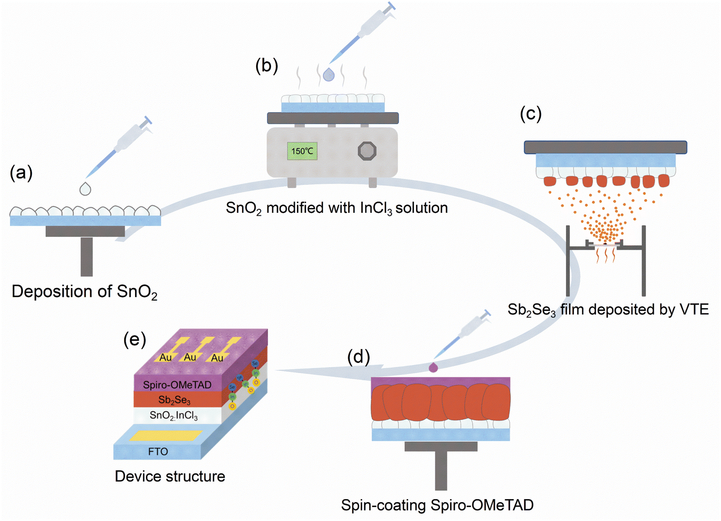 | ||
| Scheme 1 The fabrication process of an Sb2Se3 based solar cell. (a) Deposition of SnO2. (b) SnO2 modified with InCl3 solution. (c) Sb2Se3 film deposited by VTE. (d) Spin-coating Spiro-OMeTAD. (e) Device structure. | ||
Experimental
Preparation of SnO2 and InCl3 modified SnO2 layers
Before the deposition of SnO2 and the modification of SnO2 with InCl3, FTO-coated glasses should be cleaned with deionized (DI) water, isopropanol, acetone, and ethanol for 40 minutes sequentially. A UV ozone cleaner (HF-Kejing, PCE-22-LD) was employed to clean the organic residues on the surface of FTO-coated glasses. Then, the SnO2 film was prepared by spin coating SnO2 precursor solution at 2000 rpm for 40 s and, subsequently, a post annealing treatment at 200 °C for 30 min. In this process, the SnO2 precursor solution was prepared by mixing a commercial SnO2 aqueous colloidal dispersion (15 wt%, Alfa Aesar) with deionized water (1![[thin space (1/6-em)]](https://www.rsc.org/images/entities/char_2009.gif) :1 v/v). The InCl3 modified SnO2 layer was prepared by spin-coating InCl3 solution at 3000 rpm for 30 s and baking in a N2 atmosphere at 200 °C for 30 min. In this process, the InCl3 solution was obtained by dissolving 20 mg of InCl3·4H2O powder into 1 mL absolute alcohol and then stirring until the powder was dissolved completely.
:1 v/v). The InCl3 modified SnO2 layer was prepared by spin-coating InCl3 solution at 3000 rpm for 30 s and baking in a N2 atmosphere at 200 °C for 30 min. In this process, the InCl3 solution was obtained by dissolving 20 mg of InCl3·4H2O powder into 1 mL absolute alcohol and then stirring until the powder was dissolved completely.
Fabrication of Sb2Se3 solar cells
The Sb2Se3 films were deposited on FTO/SnO2 substrates with or without InCl3 treatment by vacuum thermal evaporation under a vacuum pressure of 5.0 × 10⁻⁴ Pa. The substrate temperature was controlled at 300 °C. High-purity Sb2Se3 powder (99.99%, Zhongnuoxincai) was used as the evaporation source and the evaporation rate was 40–120 nm s−1. Then, the as-deposited Sb2Se3 thin film was annealed at 300 °C for 30 min. After the post-annealing treatment, Spiro-OMeTAD was spin-coated on the surface of Sb2Se3 films at 3000 rpm for 30 s and baked at 100 °C for 10 min. Finally, a Au electrode was deposited using a thermal evaporator under a pressure of 5.0 × 10⁻⁴ Pa. The active area of the device was defined as 0.105 cm2.Chemical and morphological characterization
X-Ray diffraction (XRD) patterns were recorded using a Bruker Advance D8 diffractometer with Cu Kα radiation (λ = 1.5406 Å). The surface and cross-sectional images of SnO2, Sb2Se3 thin films, and the devices were recorded using a field emission scanning electron microscope (SEM, Hitachi SU8220) equipped with an energy dispersive spectroscopy (EDS) module (Bruker). X-Ray photoelectron spectroscopy (XPS, Thermal Scientific K-Alpha+ an instrument equipped with a monochromatic Al Kα X-ray source) were used to characterize the chemical composition of SnO2 and Sb2Se3. The synchrotron radiation photoemission spectroscopy (SRPES) spectra of Sn 3d and O 1s were measured at the BL11U beamline in the National Synchrotron Radiation Laboratory (NSRL) in Hefei, China. Atomic force microscope (AFM) measurement (Bruker Dimension Edge) was performed to characterize the roughness of SnO2 and Sb2Se3 films. Ultraviolet-visible (UV-vis) spectroscopy (SOLID3700) was used to measure the light absorption of SnO2 and Sb2Se3 thin films. Ultraviolet photo-electron spectroscopy (UPS) were measured conducted to detect the Fermi level and valence band of SnO2 and Sb2Se3 using a PHI5000 VersaProbe III (Scanning ESCA Microprobe) SCA (Spherical Analyzer) and a He(I) discharge lamp (21.2 eV). Raman spectra were recorded using a Renishaw Raman spectrometer with 532 nm laser excitation. Secondary ion mass spectrometry (SIMS) was conducted to analyse the distribution of In and Cl elements at the interfaces and their diffusion into the Sb2Se3 film.Optical and electrical characterization studies of the devices
Current density–voltage (J–V) curves of the Sb2Se3 solar cells were recorded using a standard xenon lamp solar simulator illumination with a Keithley 2400 digital Source-Meter under AM 1.5G illuminations (100 mW cm−2) in ambient air at room temperature. A halogen lamp single source illumination system combined with a monochromator is used to measure the incident photon-to-current conversion efficiency (model SPIEQ200). Electrochemical impedance spectroscopy (EIS) were obtained using a Zahner Mess System PP211 electrochemical workstation at a bias potential of −0.5 V in the dark. Transient absorption spectroscopy (TAS) of the Sb2Se3 thin films were measured using a commercial Helios setup from Ultrafast Systems. Additionally, the pump and probe laser pulses were generated by frequency doubling the fundamental output (Coherent Vitesse, 80 MHz, Ti-sapphire laser) and through white light generated with a sapphire plate, respectively. The decay kinetics are fitted using the biexponential model y = ∑Aiexp(−x/τi), and carrier lifetime (τ) was obtained using equation τ = ∑Aiτi2/∑Aiτi (i = 2). Deep level transient spectrum (DLTS) measurement was performed via a Phystech FT-1230 HERA DLTS system equipped with a 10 mW red laser (laser pulse with 635 nm wavelength & pulse voltage: 0.5 V). A modified Boonton 7200 capacitance meter (1–75 kHz) was used to examine dynamic capacitance. The DLTS temperature scan range was from 120 to 420 K with 2 K heating intervals. The pulse mode was set as electrical (pulse voltage) and optical (laser excitation) double pulses, and they were exerted and removed simultaneously. In detail, the reverse bias, pulse voltage, pulse width (electric and optical), and period width were −0.4 V, 0.2–0.6 V, 10 ms, and 100 ms, respectively.
Results and discussion
Chemical and morphological characterization studies
In this work, SnO2 films were prepared by spin-coating a diluted commercial SnO2 aqueous colloidal dispersion, as illustrated in Scheme 1. The specific details of the preparation are presented in the Experimental section. After thermal annealing at 150 °C for 30 min, we observed that the deposited SnO2 film on FTO-coated glasses is composed of nanoparticles (Fig. 1a) and exhibited uniform and compact morphology. After treating SnO2 with InCl3, the film becomes denser and flatter (Fig. 1b), corresponding to a decrease in root-mean-square roughness (Rq) from 19.1 nm of SnO2 to 17.4 nm of InCl3 modified SnO2 (Fig. S1a and b†). The decrease in Rq is mainly due to the diffusion of the In element into the SnO2 film during the annealing process, which slightly changes its surface morphology. Here, for convenience of discussion, the SnO2 film treated with InCl3 is denoted as SnO2:InCl3.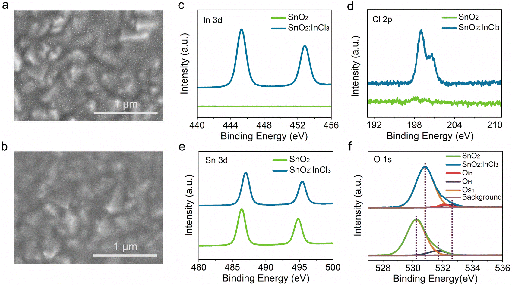 | ||
| Fig. 1 Surface SEM images of (a) SnO2 and (b) SnO2:InCl3 films. (c) High-resolution XPS spectra of (c) In 3d, (d) Cl 2p, (e) Sn 3d, and (f) O 1s elements in SnO2 and SnO2:InCl3 films. | ||
To study the surface components and chemical states of SnO2:InCl3 and SnO2, we conducted X-ray photoelectron spectroscopy (XPS) characterization. The high-resolution XPS spectra of In 3d, Cl 2p, Sn 3d and O 1s core-level regions are displayed in Fig. 1c–f. All XPS results are corrected using the reference of C 1s (284.8 eV). Notably, in the SnO2:InCl3 film, two peaks with binding energies of 445.2 eV and 452.8 eV are detected (Fig. 1c), which correspond to In 3d5/2 and In 3d3/2, respectively. Meanwhile, we detected a signal belonging to Cl 2p (Fig. 1d). The presence of In and Cl elements is due to the InCl3 post-treatment. Furthermore, the peaks at 486.4 eV and 494.8 eV can be assigned to Sn 3d5/2 and Sn 3d3/2 of the SnO2 film (Fig. 1e), while the two peaks in the SnO2:InCl3 film shift 0.6 eV towards high binding energy. This phenomenon is mainly due to the doping of the In element into SnO2 as an electron acceptor, which leads to the electron transfer from Sn to In, thereby increasing the binding energy of Sn. Likewise, as shown in Fig. 1f, the O 1s peak of the SnO2:InCl3 film can be divided into three peaks at 530.8 eV, 532.1 eV and 532.6 eV, corresponding to O–Sn (OSn), O–In (OIn) and adsorbed oxygen (OH), respectively. Compared with pristine SnO2, the OSn and OH peaks in the SnO2:InCl3 film also exhibit higher binding energy due to the formation of an In–O bond. Combined with the detected In and Cl elements, we demonstrate the formation of an InOXCl3−2X phase.29 Furthermore, we applied synchrotron radiation photoemission spectroscopy (SRPES) to measure the Sn Cl 3d and O 1s at different photon energies (Fig. 2Sa and b†). The elemental composition at different depths was detected by adjusting incident photon energies of 600, 800, 1486, and 2984 eV. With an increase in incident photon energy, that is, the detection depth deepened, the Sn 3d and O 1s peaks moved towards low binding energy, which indicates that In is mainly enriched on the surface of the SnO2 film and gradually decreases with an increase in the depth.30
The transmittance spectra of FTO, FTO/SnO2, and FTO/SnO2:InCl3 are shown in Fig. 2a. Notably, the deposited SnO2 layer improves the transmittance of FTO glass in the wavelength range from 300 nm to 700 nm. This result is due to the decrease in surface roughness of FTO/SnO2, reducing the light scattering and improving the flat transmittance of light.31 After treatment with InCl3, FTO/SnO2 exhibits no significant change in transmittance compared to pristine SnO2, which is due to the wider band gap of the formed InOXCl3−2X that avoids additional absorption. As shown in Fig. S3a and b,† the calculated bandgaps (Eg) of SnO2 and SnO2:InCl3 are both 3.94 eV according to the Tauc plot.
| (αhν)n = A(hν − Eg) |
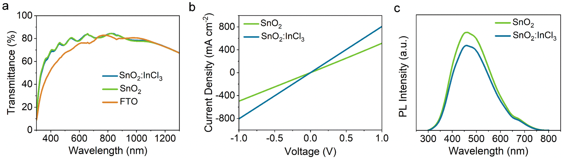 | ||
| Fig. 2 (a) Transmission spectra of FTO substrates, and the FTO substrates coated with SnO2 and SnO2:InCl3 layers. (b) Current density–voltage curves of SnO2 and SnO2:InCl3 films. (c) PL spectra of SnO2 and SnO2:InCl3 films. | ||
In order to study the influence of InCl3 treatment on the electrical properties of the SnO2 ETL, we tested the conductivity of SnO2 and SnO2:InCl3. Fig. 2b shows the current density–voltage (J–V) curves of the devices with structures of FTO/SnO2/Au and FTO/SnO2:InCl3/Au. From the slopes of the curves, we obtained the conductivity (σ0) of the films according to equation I = σ0Ad−1V, where A and d represent the area and thickness of the samples, respectively. From this, a larger slope indicates a higher conductivity. After the InCl3 treatment, SnO2:InCl3 exhibits a steeper slop than pristine SnO2, indicating that InCl3 treatment reduces the defect concentration. The corresponding J1/2–V curves are presented in Fig. S4† and the carrier mobilities are calculated using the Mott–Gurney formula J = 9/8ε0εrμ![[V with combining circumflex]](https://www.rsc.org/images/entities/i_char_0056_0302.gif) 2/
2/![[d with combining circumflex]](https://www.rsc.org/images/entities/i_char_0064_0302.gif) 3, where J, ε0, εr, μ, V, and d represent the current density, the vacuum dielectric constant, the relative dielectric constant of the electron transport layer, the electron mobility, the voltage, and the film thickness, respectively. Accordingly, the carrier mobilities of SnO2 and SnO2:InCl3 were calculated to be 2.96 × 10⁻⁴ cm2 V−1 s−1 and 1.88 × 10⁻⁴ cm2 V−1 s−1, respectively. The increase in conductivity and carrier mobility can be attributed to the passivation of deep-level defects in SnO2 films, which is beneficial for improving charge transfer at the interface of Sb2Se3/ETLs. Subsequently, steady-state photoluminescence (PL) spectroscopy was conducted to demonstrate the changes in defects in SnO2 films before and after InCl3 treatment. As shown in Fig. 2c, the SnO2 film treated with InCl3 shows a weakened PL signal. Since the PL intensity is proportional to the defect concentration, the decreased intensity indicates that InCl3 treatment reduces the defect concentration as well as the carrier recombination in SnO2 ETLs.32
3, where J, ε0, εr, μ, V, and d represent the current density, the vacuum dielectric constant, the relative dielectric constant of the electron transport layer, the electron mobility, the voltage, and the film thickness, respectively. Accordingly, the carrier mobilities of SnO2 and SnO2:InCl3 were calculated to be 2.96 × 10⁻⁴ cm2 V−1 s−1 and 1.88 × 10⁻⁴ cm2 V−1 s−1, respectively. The increase in conductivity and carrier mobility can be attributed to the passivation of deep-level defects in SnO2 films, which is beneficial for improving charge transfer at the interface of Sb2Se3/ETLs. Subsequently, steady-state photoluminescence (PL) spectroscopy was conducted to demonstrate the changes in defects in SnO2 films before and after InCl3 treatment. As shown in Fig. 2c, the SnO2 film treated with InCl3 shows a weakened PL signal. Since the PL intensity is proportional to the defect concentration, the decreased intensity indicates that InCl3 treatment reduces the defect concentration as well as the carrier recombination in SnO2 ETLs.32
In superstrate solar cells, an ETL is not only used for transporting electrons, but also has a significant impact on the quality of the subsequent deposited absorber layer. To investigate the influence of substrates on the absorber layer of Sb2Se3, we deposited Sb2Se3 films on SnO2 and SnO2:InCl3 by thermal evaporation. For convenience, the Sb2Se3 films deposited on SnO2 and SnO2:InCl3 are denoted as SnO2/Sb2Se3 and SnO2:InCl3/Sb2Se3, respectively. The XRD patterns of the two samples are shown in Fig. 3e. Except for the peaks from the FTO substrate, all peaks can be indexed to orthorhombic Sb2Se3 (JCPDS no. 15-0681). In the Raman spectrum (Fig. S5†), both films exhibit three dominant peaks corresponding to the Sb2Se3 phase at 151, 189, and 209 cm−1. Based on the above results, we confirm that the Sb2Se3 films deposited by VTE have high purity.
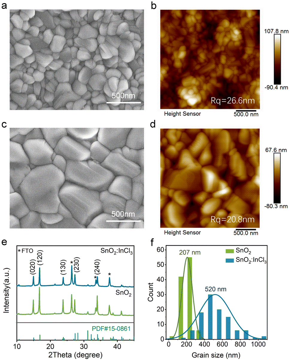 | ||
| Fig. 3 Surface SEM images of Sb2Se3 films on (a) SnO2 and (c) SnO2:InCl3 layers. AFM images of Sb2Se3 films on (b) SnO2 and (d) SnO2:InCl3. (e) XRD patterns of the Sb2Se3 films that were deposited on SnO2 and SnO2:InCl3 films, with FTO as the substrate. (f) Statistical distribution of the grain size in Sb2Se3 films on SnO2 and SnO2:InCl3 films. | ||
Furthermore, the treatment of SnO2 ETLs significantly changed the morphology of Sb2Se3 films, as shown in the SEM images in Fig. 3a–c. The InCl3-modified SnO2 increases the average grain size of Sb2Se3 from about 200 nm to 500 nm (Fig. 3f and S6†), which can reduce the recombination loss at grain boundaries (GBs). Moreover, compared with the Sb2Se3 film on SnO2, the surface morphology of the Sb2Se3 film deposited on SnO2:InCl3 is flatter, with Rq decreasing from 26.6 to 20.8 nm (Fig. 3b–d), which is favourable to improving the contact between the absorber layer and hole transport layer, thereby reducing the leakage current of the solar cell.
To probe the impact of InCl3 post-treatment on the energy level alignment between SnO2 and Sb2Se3, ultraviolet photoelectron spectroscopy (UPS) was used to measure the valence band maximum (VBM) and Fermi level (EF). As shown in Fig. 4a–d, the EF of SnO2 and SnO2:InCl3 are measured to be −3.95 and −4.28 eV, respectively. By linear extrapolation of the low binding energy region, the gaps (EP) between the Fermi level and valence band maximum are estimated to be 3.55 and 3.38 eV for SnO2 and SnO2:InCl3, respectively. Combined with the same optical band gap of 3.94 eV (Fig. S3†), the conduction band minimum (CBM) corresponding to SnO2 and SnO2:InCl3 is calculated to be −3.56 eV and −3.72 eV, respectively. Similarly, the Eg, EF, EP and CBM of Sb2Se3 deposited on the SnO2 and SnO2:InCl3 substrates are measured to be 1.25 eV, −4.70 eV, 0.47 eV, and −3.97 eV and 1.25 eV, −4.54 eV, 0.51 eV, and −3.85 eV, respectively (Fig. 4b–d).22 The schematic diagrams of energy level alignment between the ETL and Sb2Se3 films are shown in Fig. 4e and f. Consequently, the conduction band offset (CBO) of SnO2/Sb2Se3 and SnO2:InCl3/Sb2Se3 heterojunctions is calculated to be −0.41 eV (−ΔEC) and −0.13 eV (−ΔEC), respectively. Notably, both interfaces have “spike” like energy level alignment, while a mild spike (0.1 ≤ ΔEC ≤ 0.2 eV) is believed to reduce the carrier recombination.33 Therefore, the improved band alignment between SnO2:InCl3 and Sb2Se3 can facilitate efficient carrier transport in a solar cell and is expected to improve the device efficiency.
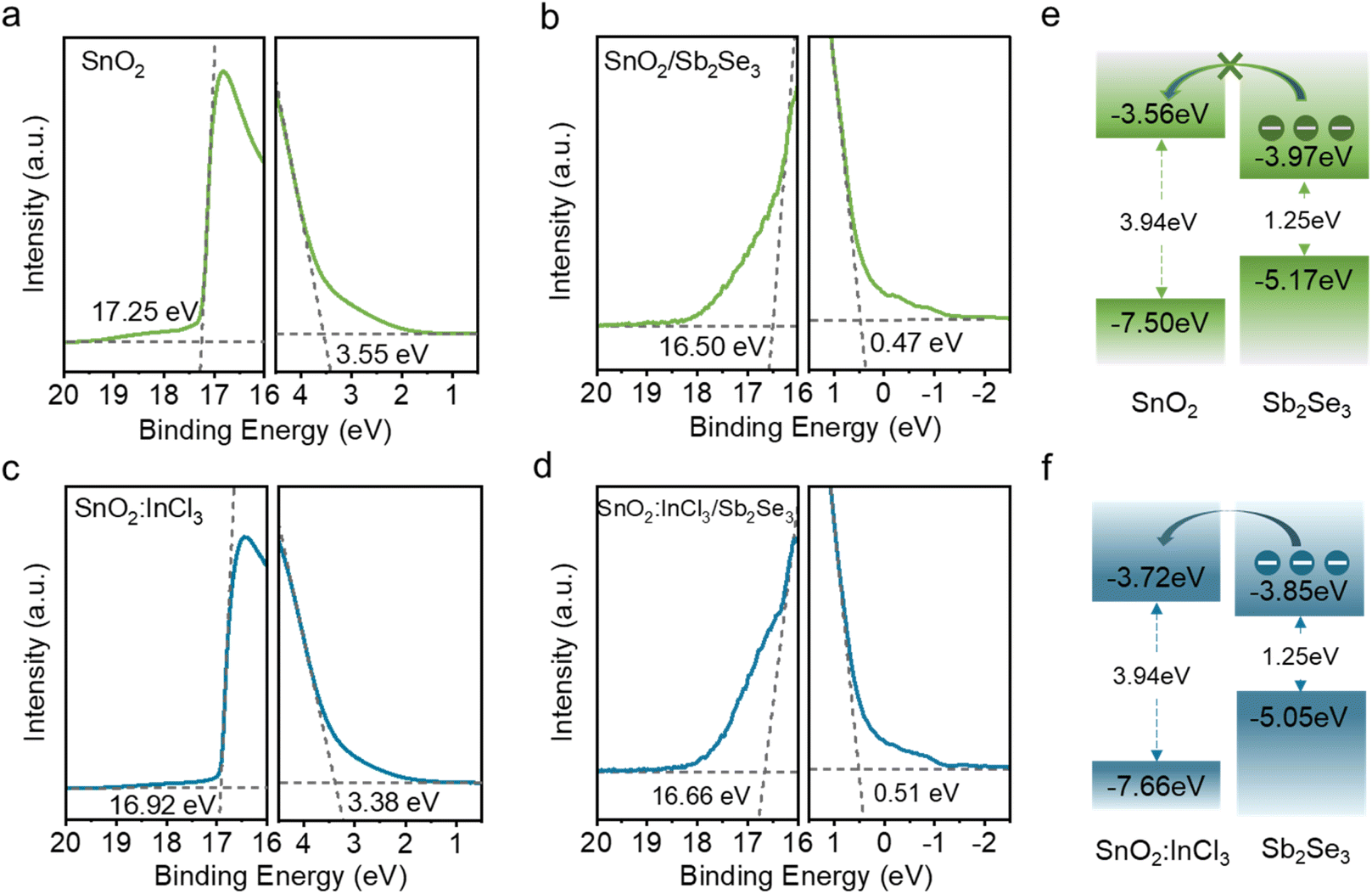 | ||
| Fig. 4 The UPS spectra of (a) SnO2, (b) SnO2/Sb2Se3, (c) SnO2:InCl3, and (d) SnO2:InCl3/Sb2Se3. A diagram of the energy band alignments at the interfaces between Sb2Se3 and (e) SnO2 and (f) SnO2:InCl3. | ||
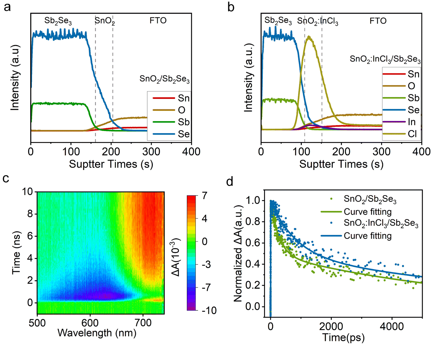
After interface treatment of SnO2, the quality of subsequently deposited Sb2Se3 films was significantly improved. In order to gain insight into the improvement mechanism of the film quality, we utilized secondary ion mass spectrometry (SIMS) to detect the vertical distribution of elements in ETLs/Sb2Se3. As shown in Fig. 5a, we observe severe diffusion of Se into the SnO2 layer in the absence of InCl3 treatment, which may lead to the formation of SnO2−xSex, resulting in a poor heterojunction.16 In contrast, InCl3 treatment hinders the diffusion of the Se element into SnO2, while allowing the Cl element to diffuse into Sb2Se3, which is beneficial for passivating defects in the absorption layer, as demonstrated in previous studies (Fig. 5d).34 Afterwards, we analyzed the bonding information at the interface through XPS. When 3 nm of the Sb2Se3 film was deposited on the SnO2:InCl3 substrate, we detected the presence of the In element in Sb2Se3 (Fig.S7†). In specific, the In 3d peak can be divided into three kinds of peaks. The peaks at 444.5 eV and 451.9 eV, 445.2 eV and 452.7 eV, and 446.0 eV and 453.5 eV can be assigned to In3+ that bonded with Se2−, O2− and Cl−, respectively. The formed In–Se and In–O bonds indicate that In serves as a bridge between SnO2 and Sb2Se3, which can improve the carrier extraction and transport at the interface.22 Thus, transient absorption spectroscopy (TAS) was performed to compare the kinetics of carrier transport at the interface of ETLs/Sb2Se3. In this measurement, a 360 nm pump pulse laser is selected as the source to excite the ground-state charge carrier in the Sb2Se3 films, and TAS spectra are obtained (Fig. 5c and S8†). Then, transition dynamics of the samples are extracted from the TAS spectrum near 690 nm wavelength and well fitted according to the double exponential decay equation, as shown in Fig. 5d. The fitted average lifetime of FTO/SnO2/Sb2Se3 and FTO/SnO2:InCl3/Sb2Se3 is 5.960 and 7.877 ns, respectively. Compared with FTO/SnO2/Sb2Se3, FTO/SnO2:InCl3/Sb2Se3 exhibits a prolonged carrier lifetime. This may be attributed to the modification of the SnO2 ETL with InCl3 improving the quality of Sb2Se3, thereby reducing the existing defects in the film.
 | ||
| Fig. 5 The secondary ion mass spectroscopy (SIMS) spectra of (a) SnO2/Sb2Se3 and (b) SnO2:InCl3/Sb2Se3. (c) TAS mapping of SnO2:InCl3/Sb2Se3. (d) Transient decay kinetics (scatter) and fit (solid lines) monitored at 690 nm for Sb2Se3 films deposited on SnO2 and SnO2:InCl3. | ||
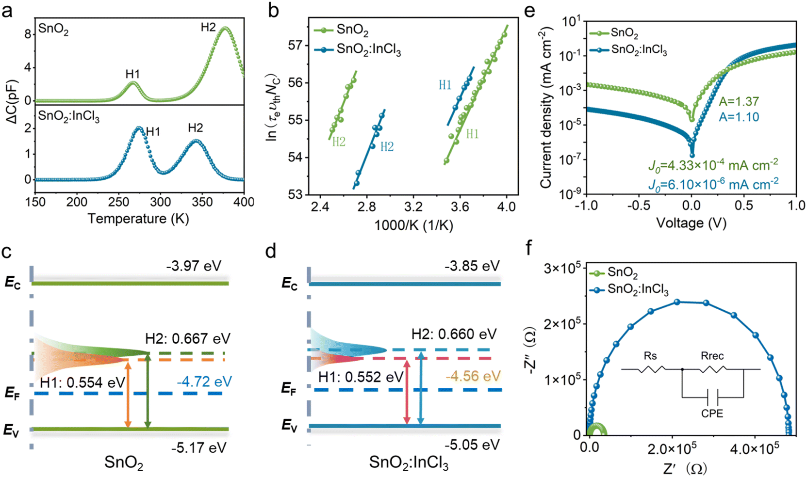
To explore the deep-level defects in the films, we conducted the deep-level transient spectroscopy (DLTS) measurement. The number of defects was identified from the DLTS signal using the Fourier deconvolution algorithm, and the corresponding trap density was calculated (the characterization details are provided in Note 1 in the ESI†). The Sb2Se3 films deposited by the vacuum thermal evaporation method in this work display p-type conductivity. Thus, the positive and negative peaks in the DLTS spectra represent hole traps (acceptor defects) and electron traps (donor defects), respectively. As shown in Fig. 6a, both samples are detected to have two dominant deep-level acceptor defects. The detailed defect parameters including the trap energy level (ET), capture cross section (σ), trap density (NT), and carrier density (NS) extracted from the DLTS spectra are summarized in Table 1. Notably, the activation energies of the trap defects in the two devices are similar, indicating that the origins of these defects are the same due to the same synthesis method. Accordingly, these two kinds of defects in the devices can be denoted as H1 and H2. Combined with the calculation results, the traps H1 and H2 located at about 0.55 and 0.66 eV above the VBM (Fig. 6c and d) can be assigned to the antimony vacancy (VSb) and selenium substitutes for antimony anti-site defects (SeSb), respectively. Both acceptor defects act as hole traps or recombination sites, which can hinder the charge transport and shorten the carrier lifetime. After the modification of SnO2 with InCl3, the trap state densities in the absorb layer are reduced compared with the control sample. The reduced defect density demonstrates that SRH recombination in the SnO2:InCl3 based device is effectively suppressed.
 | ||
| Fig. 6 Dual-pulse mode DLTS signals at variable pulse voltage (0.2–0.6 V) for (a) SnO2/Sb2Se3 and (b) SnO2:InCl3/Sb2Se3 devices. Schematic diagram of the energy band and defect level of (c) Sb–SnO2/Sb2Se3 and (d) SnO2:InCl3/Sb2Se3 devices. EC, EV, and EF stand for the CBM, Fermi level and VBM, respectively. (e) Dark J–V curves of SnO2/Sb2Se3 and SnO2:InCl3/Sb2Se3 devices. (f) Nyquist plots (under dark conditions at 0.50 V) of SnO2/Sb2Se3 and SnO2:InCl3/Sb2Se3 devices. | ||
| Devices | Trap | Defect | E T (eV) | σ (cm2) | N T (cm−3) | N S (cm−3) |
|---|---|---|---|---|---|---|
| SnO2/Sb2Se3 | H1 | VSb | E V + 0.554 | 1.71 × 10⁻¹⁴ | 5.42 × 10¹⁴ | 4.74 × 10¹⁶ |
| H2 | SeSb | E V + 0.667 | 4.53 × 10⁻¹⁶ | 6.53 × 10¹⁴ | ||
| SnO2:InCl3/Sb2Se3 | H1 | VSb | E V + 0.552 | 7.37 × 10⁻¹⁵ | 3.81 × 10¹⁴ | 4.56 × 10¹⁶ |
| H2 | SeSb | E V + 0.660 | 6.94 × 10⁻¹⁵ | 5.87 × 10¹³ |
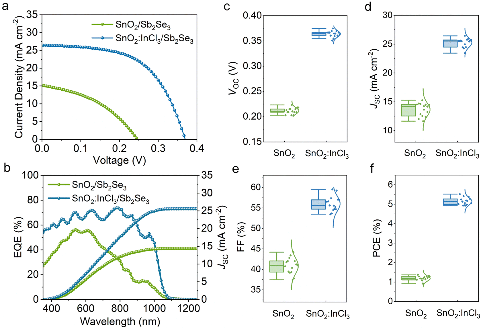
In order to explore the effect of InCl3-modified SnO2 on device performance, solar cells with the structure of FTO/SnO2 (or SnO2:InCl3)/Sb2Se3/Spiro-OMeTAD/Au were fabricated. The corresponding cross sectional SEM image of the device is shown in Fig. S9.† Current density–voltage (J–V) curves of the devices based on SnO2 and SnO2:InCl3 ETLs were measured under one solar illumination (100 mW cm−2). The J–V curves of the best devices are shown in Fig. 7a, and the detailed parameters are listed in Table 2. Notably, the SnO2-based device delivers an open circuit voltage (VOC), a short-circuit current density (JSC), a fill factor (FF), and a power conversion efficiency (PCE) of 0.243 V, 15.20 mA cm−2, 40.72%, and 1.51%, respectively. In comparison, the SnO2:InCl3-based device delivers enhanced photovoltaic parameters, corresponding to a VOC of 0.367 V, JSC of 26.44 mA cm−2, FF of 56.95%, and PCE of 5.52%. The box statistical distribution of photovoltaic parameters for the two types of devices is shown in Fig. 7c–f, which further demonstrates that using InCl3 to treat an SnO2 ETL can improve the VOC, JSC, FF, as well as PCE of Sb2Se3 devices. To understand the increase in JSC, we recorded the external quantum efficiency (EQE) spectrum of the devices (Fig. 7b). Compared with the SnO2-based device, the SnO2:InCl3-based Sb2Se3 device exhibits a higher photo-response in the wavelength range from 350 to 1050 nm, which leads to an increase in the integrated current density from 14.41 to 25.57 mA cm−2.
 | ||
| Fig. 7 a) Current density–voltage (J–V) characteristics and (b) external quantum efficiency (EQE) spectra of the optimal SnO2/Sb2Se3 and SnO2:InCl3/Sb2Se3 devices. Statistical boxplots of (c) conversion efficiency (%), (d) VOC (V), (e) fill factors (%), and (f) JSC (mA cm−2) for SnO2/Sb2Se3 and SnO2:InCl3/Sb2Se3 solar cells. | ||
| Devices | V OC (V) | J SC (mA cm−2) | FF (%) | PCE (%) |
|---|---|---|---|---|
| SnO2/Sb2Se3 | 0.243 | 15.20 | 40.72 | 1.51 |
| SnO2:InCl3/Sb2Se3 | 0.367 | 26.44 | 56.95 | 5.52 |
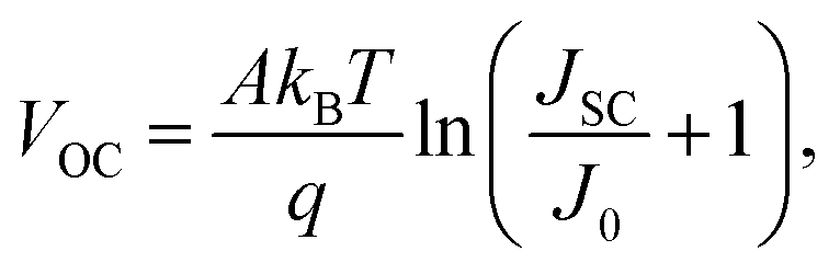
Dark J–V curves were tested to investigate the reverse saturation current (J0) and diode ideal factor (n) of the solar cells (Fig. 6e). For the SnO2:InCl3-based device, the J0 and n are estimated to be 6.10 × 10⁻⁶ mA cm−2 and 1.37, respectively, while for the SnO2-based device, J0 and n are 4.33 × 10⁻⁴ mA cm−2 and 1.10, respectively. Notably, n reflects the defect-assisted Shockley–Read–Hall (SRH) recombination properties of the film. Thus, the decreased n value indicates that Shockley–Read–Hall (SRH) recombination is effectively suppressed in the SnO2:InCl3 device due to the improvement of the interfacial contact and the reduced point defects in the Sb2Se3 film. In addition, J0 is also significantly reduced after SnO2 is treated with InCl3. According to the following equation:
We further apply EIS to characterize the interfacial charge transfer in the device. Nyquist plots and a fitting equivalent electronic circuit of the solar cells are presented in Fig. 6f, where RS and RREC correspond to series resistance and recombination resistance of the device, respectively. The device with InCl3 treatment exhibits a larger RREC of 57.84 kΩ cm2 and smaller RS of 12.83 Ω cm2 when compared with the SnO2-based device, which correspond to a RREC of 42.09 kΩ cm2 and RS of 22.57 Ω cm2. The increased RREC and decreased RS indicate that the carrier recombination in the device is effectively inhibited by using InCl3 to modify the SnO2 ETL. This result is mainly attributed to the effective passivation of defects and the improved interfacial heterojunction, thus significantly improving the efficiency of the Sb2Se3 based solar cells.
Conclusions
In summary, we demonstrated an InCl3 modified SnO2 film and its application as an ETL in Sb2Se3 solar cells. InCl3 post-treatment not only effectively prevents the diffusion of Se, but also guides the subsequent growth of Sb2Se3. The improvement of the quality of the Sb2Se3 film and the SnO2/Sb2Se3 heterojunction resulted in a device efficiency of 5.52% for Sb2Se3 solar cells, which is currently the highest efficiency among Sb2Se3 solar cells based on SnO2 electron transport layers. Thus, this work offers a simple and effective method for improving the quality of Sb2Se3 films deposited on metal oxide substrates and provides a new path towards fabricating Cd-free Sb2Se3 solar cells.Author contributions
T. C., R. F. T. and L. H. conceived and designed the study. L. H. provided samples for the study. J. J. Y. performed the DLTS experiment and analysed the data. P. X. performed the TAS experiment and analysed the data. A. X. L. performed the XRD experiments. R. F. T. and Y. W. performed the XPS experiments and analysed the data. Y. J. X. performed the SRPES experiments and analysed the data. H. L. C. provided the method for preparing SnO2 films. T. C., C. F. Z., R. F. T. and H. L. interpreted the data. T. C., R. F. T. and X. S. L. revised the manuscript. All authors contributed to the general discussion.Conflicts of interest
The authors declare no conflict of interest.Acknowledgements
This work was supported by the National Key Research and Development Program of China (2019YFA0405600), National Natural Science Foundation of China (22005293, U19A2092 and 22275180), Institute of Energy, Hefei Comprehensive National Science Center (Grant No. 21KZS212), and Collaborative Innovation Program of Hefei Science Center, CAS.Notes and references
- R. Tang, X. Wang, W. Lian, J. Huang, Q. Wei, M. Huang, Y. Yin, C. Jiang, S. Yang, G. Xing, S. Chen, C. Zhu, X. Hao, M. A. Green and T. Chen, Nat. Energy, 2020, 5, 587–595 CrossRef CAS.
- A. Polman, M. Knight, E. C. Garnett, B. Ehrler and W. C. Sinke, Science, 2016, 352, aad4424 CrossRef PubMed.
- J. Zhang, W. Lian, Y. Yin, X. Wang, R. Tang, C. Qian, X. Hao, C. Zhu and T. Chen, Sol. RRL, 2020, 4, 2000048 CrossRef CAS.
- Y. C. Choi, T. N. Mandal, W. S. Yang, Y. H. Lee, S. H. Im, J. H. Noh and S. I. Seok, Angew. Chem., 2014, 53, 1329–1333 CrossRef CAS.
- Y. Zhou, M. Leng, Z. Xia, J. Zhong, H. Song, X. Liu, B. Yang, J. Zhang, J. Chen, K. Zhou, J. Han, Y. Cheng and J. Tang, Adv. Energy Mater., 2014, 4, 1301846 CrossRef.
- X. Liang, Y. Feng, W. Dang, H. Huang, X. Wang, Y. Guo, K. Shen, R. E. I. Schropp, Z. Li and Y. Mai, ACS Energy Lett., 2022, 8, 213–221 CrossRef.
- Z. Duan, X. Liang, Y. Feng, H. Ma, B. Liang, Y. Wang, S. Luo, S. Wang, R. E. I. Schropp, Y. Mai and Z. Li, Adv. Mater., 2022, 34, e2202969 CrossRef PubMed.
- G. Liang, Y. Luo, S. Chen, R. Tang, Z. Zheng, X. Li, X. Liu, Y. Liu, Y. Li, X. Chen, Z. Su, X. Zhang, H. Ma and P. Fan, Nano energy, 2020, 73, 104806 CrossRef CAS.
- C. Jiang, R. Tang, C. Zhu and T. Chen, J. Univ. Sci. Technol., 2020, 50, 1383 CAS.
- Y. Zhao, S. Wang, C. Li, B. Che, X. Chen, H. Chen, R. Tang, X. Wang, G. Chen, T. Wang, J. Gong, T. Chen, X. Xiao and J. Li, Energy Environ. Sci., 2022, 15, 5118–5128 RSC.
- Y. Yin, C. Jiang, Y. Ma, R. Tang, X. Wang, L. Zhang, Z. Li, C. Zhu and T. Chen, Adv. Mater., 2021, 33, e2006689 CrossRef.
- Y. Zhou, L. Wang, S. Chen, S. Qin, X. Liu, J. Chen, D.-J. Xue, M. Luo, Y. Cao, Y. Cheng, E. H. Sargent and J. Tang, Nat. Photonics, 2015, 9, 409–415 CrossRef CAS.
- X. Jin, Y. Fang, T. Salim, M. Feng, Z. Yuan, S. Hadke, T. C. Sum and L. H. Wong, Adv. Mater., 2021, 33, e2104346 CrossRef PubMed.
- C. Liu, S. Wu, Y. Gao, Y. Feng, X. Wang, Y. Xie, J. Zheng, H. Zhu, Z. Li, R. E. I. Schropp, K. Shen and Y. Mai, Adv. Funct. Mater., 2022, 32, 2209601 CrossRef CAS.
- Y. Zhao, C. Li, J. Niu, Z. Zhi, G. Chen, J. Gong, J. Li and X. Xiao, J. Mater. Chem. A, 2021, 9, 12644–12651 RSC.
- L. Wang, D.-B. Li, K. Li, C. Chen, H.-X. Deng, L. Gao, Y. Zhao, F. Jiang, L. Li, F. Huang, Y. He, H. Song, G. Niu and J. Tang, Nat. Energy, 2017, 2, 1903914 Search PubMed.
- K. Li, C. Chen, S. Lu, C. Wang, S. Wang, Y. Lu and J. Tang, Adv. Mater., 2019, 31, 1903914 CrossRef CAS PubMed.
- L. Xiong, Y. Guo, J. Wen, H. Liu, G. Yang, P. Qin and G. Fang, Adv. Funct. Mater., 2018, 28, 1802757 CrossRef.
- J. Tao, X. Hu, Y. Guo, J. Hong, K. Li, J. Jiang, S. Chen, C. Jing, F. Yue, P. Yang, C. Zhang, Z. Wu, J. Tang and J. Chu, Nano Energy, 2019, 60, 802–809 CrossRef CAS.
- Z. Zhang, M. Hu, T. Jia, J. Du, C. Chen, C. Wang, Z. Liu, T. Shi, J. Tang and Y. Leng, ACS Energy Lett., 2021, 6, 1740–1748 CrossRef CAS.
- W. Wang, L. Yao, J. Dong, L. Wu, Z. Cao, L. Hui, G. Chen, J. Luo and Y. Zhang, Adv. Mater. Interfaces, 2022, 9, 2102464 CrossRef CAS.
- X. Meng, X. Cui, M. Rager, S. Zhang, Z. Wang, J. Yu, Y. Harn, Z. Kang, B. Wagner, Y. Liu, C. Yu, J. Qiu and Z. Lin, Nano Energy, 2018, 52, 123–133 CrossRef CAS.
- Y. Ma, X. Meng, K. Li, L. Zhang, Y. Du, X. Cai and J. Qiu, ACS Catal., 2023, 13, 1290–1298 CrossRef CAS.
- X. Meng, C. Yu, X. Song, J. Iocozzia, J. Hong, M. Rager, H. Jin, S. Wang, L. Huang, J. Qiu and Z. Lin, Angew. Chem., Int. Ed., 2018, 57, 4682–4686 CrossRef CAS.
- S. Bi, X. Leng, Y. Li, Z. Zheng, X. Zhang, Y. Zhang and H. Zhou, Adv. Mater., 2019, 31, 1805708 CrossRef CAS.
- Z. Gao, Y. Wang and W. Choy, Adv. Energy Mater., 2022, 12, 2104030 CrossRef CAS.
- Y. Wang, R. Tang, L. Huang, C. Qian, W. Lian, C. Zhu and T. Chen, ACS Appl. Mater. Interfaces, 2022, 14, 33181–33190 CrossRef CAS.
- W. Wang, Z. Cao, H. Wang, J. Luo and Y. Zhang, J. Mater. Chem. A, 2021, 9, 26963–26975 RSC.
- X. Guo, J. Du, Z. Lin, J. Su, L. Feng, J. Zhang, Y. Hao and J. Chang, Chem. Eng. J., 2021, 407, 127997 CrossRef CAS.
- J. Ge, D. He, W. Chen, H. Ju, H. Zhang, T. Chao, X. Wang, R. You, Y. Lin, Y. Wang, J. Zhu, H. Li, B. Xiao, W. Huang, Y. Wu, X. Hong and Y. Li, J. Am. Chem. Soc., 2016, 138, 13850–13853 CrossRef CAS.
- Y. Zhao, J. Duan, H. Yuan, Y. Wang, X. Yang, B. He and Q. Tang, Sol. RRL, 2019, 3, 1800284 CrossRef.
- C. Chen, Y. Zhao, S. Lu, K. Li, Y. Li, B. Yang, W. Chen, L. Wang, D. Li, H. Deng, F. Yi and J. Tang, Adv. Energy Mater., 2017, 7, 1700866 CrossRef.
- H. Shiel, O. S. Hutter, L. J. Phillips, J. E. N. Swallow, L. A. H. Jones, T. J. Featherstone, M. J. Smiles, P. K. Thakur, T.-L. Lee, V. R. Dhanak, J. D. Major and T. D. Veal, ACS Appl. Energy Mater., 2020, 3, 11617–11626 CrossRef CAS.
- S. Chen, M. Li, Y. Zhu, X. Cai, F. Xiao, T. Ma, J. Yang, G. Shen, A. Ke, Y. Lu, W. Liang, H. Hsu, C. Chen, J. Tang and H. Song, Adv. Energy Mater., 2022, 12, 2202897 CrossRef CAS.
Footnotes |
| † Electronic supplementary information (ESI) available. See DOI: https://doi.org/10.1039/d3ta03358a |
| ‡ These authors contributed equally to this work. |
| This journal is © The Royal Society of Chemistry 2023 |