
 Open Access Article
 This Open Access Article is licensed under a Creative Commons Attribution-Non Commercial 3.0 Unported Licence
SbSeI and SbSeBr micro-columnar solar cells by a novel high pressure-based synthesis process†
Ivan
Caño
*ab,
Alejandro
Navarro-Güell
ab,
Edoardo
Maggi
ab,
Maria
Barrio
c,
Josep-Lluís
Tamarit
 bc,
Simon
Svatek
d,
Elisa
Antolín
d,
Shunya
Yan
e,
Esther
Barrena
e,
Beatriz
Galiana
f,
Marcel
Placidi
ab,
Joaquim
Puigdollers
ab and
Edgardo
Saucedo
ab
bc,
Simon
Svatek
d,
Elisa
Antolín
d,
Shunya
Yan
e,
Esther
Barrena
e,
Beatriz
Galiana
f,
Marcel
Placidi
ab,
Joaquim
Puigdollers
ab and
Edgardo
Saucedo
ab
aUniversitat Politècnica de Catalunya (UPC), Photovoltaic Lab – Micro and Nano Technologies Group (MNT), Electronic Engineering Department, EEBE, Av Eduard Maristany 10-14, Barcelona 08019, Catalonia, Spain. E-mail: ivan.cano.prades@upc.edu
bUniversitat Politècnica de Catalunya (UPC), Barcelona Centre for Multiscale Science & Engineering, Av Eduard Maristany 10-14, Barcelona 08019, Catalonia, Spain
cUniversitat Politècnica de Catalunya (UPC), Group of Characterization of Materials (GCM), Physics Department, EEBE, Av Eduard Maristany 10-14, Barcelona 08019, Catalonia, Spain
dInstituto de Energía Solar, Universidad Politécnica de Madrid (UPM), Av. Complutense, 30, Madrid 28040, Spain
eInstitut de Ciència de Materials de Barcelona (ICMAB), Carrer dels Til·lers, Bellaterra 08193, Spain
fUniversidad Carlos III de Madrid, Physics Department, Av. Universidad 40, Leganés 28911, Spain
First published on 20th July 2023
Abstract
Van der Waals chalcogenides and chalcohalides have the potential to become the next thin film PV breakthrough, owing to the earth-abundancy and non-toxicity of their components, and their stability, high absorption coefficient and quasi-1D structure, which leads to enhanced electrical anisotropic properties when the material is oriented in a specific crystalline direction. However, quasi-1D semiconductors beyond Sb2(S,Se)3, such as SbSeX chalcohalides, have been scarcely investigated for energy generation applications, and rarely synthesised by physical vapor deposition methodologies, despite holding the promise of widening the bandgap range (opening the door to tandem or semi-transparent devices), and showing enticing new properties such as ferroelectric behaviour and defect-tolerant nature. In this work, SbSeI and SbSeBr micro-columnar solar cells have been obtained for the first time by an innovative methodology based on the selective halogenation of Sb2Se3 thin films at pressure above 1 atm. It is shown that by increasing the annealing temperature and pressure, the height and density of the micro-columnar structures grows monotonically, resulting in SbSeI single-crystal columns up to 30 μm, and tuneable morphology. In addition, solar cell prototypes with substrate configuration have shown remarkable Voc values above 550 mV and 1.8 eV bandgap.
Introduction
Despite some studies in the 80s pointing to their promise to develop photoelectrochemical solar cells (see R. N. Bhattacharya and P. Pramanik),1 quasi-1D van der Waals semiconductors have been largely overlooked as potential photoabsorbers for photovoltaics (PV). However, since the first Sb2Se3 PV conversion efficiencies were reported in 2009, their performance has increased consistently, triplicating between 2014 and 2023, and surpassing the 10% threshold in 2022.2–5 In addition, quasi-1D chalcogenides entail many benefits compared to other PV thin film systems, including the earth-abundancy and low toxicity of their components, their high stability, large absorption coefficients (up to 105 cm−1) and anisotropic crystal structure, which results in unique electrical properties that can enhance the PV performance when the material is correctly oriented.6Surprisingly, van der Waals semiconductors beyond Sb2Se3 and Sb2S3 have been barely investigated for energy generation applications. However, it is expected that combinations of chalcogenides and halides with group V cations, having differences in electronegativity smaller than 1.7 eV, will result in quasi-1D materials with an analogous structure to Sb2Se3, yet comprising a broad range of optoelectronic properties, including variable bandgap and conductivity. For instance, recent studies have demonstrated that cation-substitution with Bi – (Sb1−xBix)2Se3 – leads to semiconductors with bandgaps below 1.0 eV,7,8 while SbSeX chalcohalides (X = I, Br) have bandgaps in the wider 1.7–2.0 eV range;9,10 making them ideal for tandem or semi-transparent PV applications. Chalcohalides have also been reported to possess ferroelectric properties, whereby a small displacement along their c-axis switches between centrosymmetric and non-centrosymmetric structures (Pnam to Pna21 respectively) resulting in a ferroelectric transition.11 Ferroelectricity in chalcohalides has been known for a long time. Indeed, E. Fatuzzo reported as early as in 1962 that “SbSI is the first ferroelectric material which is also photoconductive”.12 Surprisingly, the impact of photoferroics in PV laid largely dormant until the discovery of ferroelectric oxide perovskites (BaTiO3 or BiFeO3), which show open-circuit voltages exceeding the value of the bandgap.13,14 This abnormal photovoltaic effect, which is still the object of scientific inquiry, might originate from the presence of a non-zero dipole in the crystal unit cell, resulting in ferroelectric domains. Thus, if the gradients in the electrical potential do not cancel each other, a voltage generated across the crystal could exceed the value of bandgap. In light of the above, ferroelectric chalcohalides may offer new opportunities (or an alternative to perovskites) to improve electron–hole separation by means of a spontaneous polarization, as well as achieving higher photovoltages.
In addition, it has been reported that SbSeX and SbSX materials might have excellent defect-tolerant properties suitable for PV. Indeed, first-principle calculations have shown that group V chalcohalides exhibit a similar band structure to that of the successful MAPbI3 perovskite, the defect-tolerant nature of which likely emerges from having bonding orbitals at the conduction band, and antibonding orbital contributions at the valence band maximum.15 However, this is a necessary but not sufficient condition towards defect-tolerance, and band alignment or structural considerations may also have an impact on the likelihood of a material to produce deep levels leading to adverse recombination processes.16 Overall, SbSeX chalcohalides meet all the requirements to develop excellent photoabsorbers for PV, as well as for other state-of-the-art applications including thermoelectrics, piezo-, and triboelectrics.17
The first attempts to synthesise these materials for PV implementation have been essentially focused on low temperature (<300 °C) and atmospheric pressure solution-based chemical routes, although PV performance of the resulting devices has been overall low. Y. C. Choi and K. W. Jung have demonstrated a natural tendency of the SbSeI to form one-dimensional columnar-like structures, with high crystalline quality, when prepared from a mixture of SbCl3 and selenourea, and SbI3 solutions.18 They have also reported a similar two-step process to synthesise Sb(S,Se)I.19 Following this procedure, SbSeI solar cells were manufactured with efficiencies slightly above 0.2%. However, recent progresses by R. Nie et al., have yielded conversion efficiencies above 4%, using an organic–inorganic hybrid solar cell architecture, with SbSeI grown in a matrix of mesoporous (mp)-TiO2.20 Interestingly, SbSeI can also be synthesised by a topotactic conversion from Sb2Se3, highlighting its flexibility in terms of processing.21
Nonetheless, no attempts have yet been reported to prepare chalcohalide solar cells by physical vapor deposition (PVD) methodologies, although they have been the most successful techniques for synthesizing high-efficiency chalcogenide devices including Sb2Se3,4,22 and provide many advantages and opportunities. For instance, they do not involve solvents or organic chemicals, leading to a cleaner approach to materials synthesis, largely avoiding contamination and formation of unwanted phases. Also, their high reproducibility and versatility make them particularly suitable to explore compositions and alloys that would be difficult to achieve by chemical routes, as well as combinatorial experiments.
It is likely that the higher volatility of halogen/halide compounds, compared to those of Sb or even Se, has been the bottleneck to the development of SbSeI by vacuum-based methods. Indeed, I2 and SbI3 have larger vapor pressures than Se or Sb's at any temperature, see Fig. 1a.23 Consequently, finding the suitable annealing conditions to achieve the necessary halide reactive atmosphere to synthesise the material poses a number of distinct challenges. In particular, due to their high vapor pressure, in a vacuum system it is indeed highly complex to establish an appropriate configuration to obtain stable compositions, as well as to effectively tune the growth conditions and morphology of the material. In order to have a more controlled, reproducible and scalable system, here we propose the synthesis of chalcohalide samples by using a novel process based on a selective iodination/bromination of Sb2Se3 thin films at pressures higher than 1 atm. Thus, we expand the versatility of the method by including the possibility of adjusting the growth conditions by three variables (time, temperature, pressure), with an extended pressure range above atmospheric conditions. Working under such conditions increases the halide's sublimating point (solid + vapor equilibrium), hence reducing its volatility, which allows to prepare materials containing Se and iodine/bromine-based compounds for an extended heating time without loss of neither halide nor chalcogen, achieving stable stoichiometric compositions. Moreover, the coordinated variation of temperature and pressure opens the door to the development of new strategies to adjust the morphology and structure of the sample in a more precise and fine way.
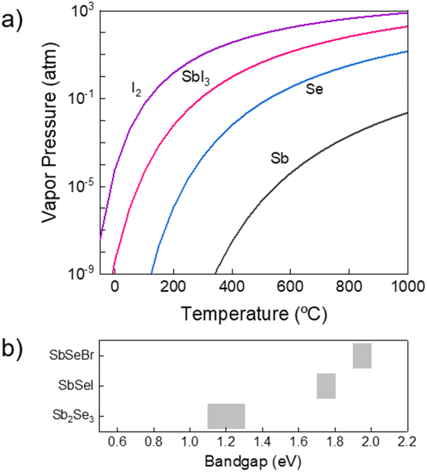 | ||
| Fig. 1 (a) Vapor pressure of I2, Se and Sb as a function of temperature. (b) Bandgap range of Sb2Se3, SbSeI and SbSeBr from literature.25–28 | ||
In this work, SbSeX (X = I, Br) samples have been successfully synthesised for the first time using this high-pressure method under different growing conditions, developing single-crystal micro-columnar structures, whose height and density can be tuned by finely varying the annealing temperature and pressure. In addition, its formation mechanism has been studied, pointing towards new synthesis routes and a broader understanding of the material. Optoelectronic properties have been studied in two ways. First, electrical measurements of single crystals show n-type conductivity (which is studied by comparing the current–voltage response of the absorber in a metal/semiconductor junction with lower and higher work function metals), and a diode response with photoactive performance. Finally, SLG/Mo/SbSeI/CdS/ZnO/ITO prototype solar cell devices have been fabricated, showing bandgap in the 1.7–2.0 eV range, and photogenerated voltages above 550 mV, which are amongst the highest reported for chalcohalide solar cells. Although the carrier collection is still poor due to an unoptimized device architecture, these results demonstrate the potential of a novel emerging earth-abundant PV technology based on SbSeI micro-columnar absorbers.
Overall, we believe that the novel high pressure-based PVD procedure holds potential to be extended to further chalcohalide compositions involving volatile components, such as SbSX (X = Cl, Br, I) and Bi chalcohalides (e.g. BiSX BiSeX), opening the field of a diverse and promising new family of wider-bandgap van der Waals materials. However, Br and I are the most interesting halides specifically for PV applications, since the bandgaps resulting from these elements lie in the 1.5 to 2.0 eV range (visible spectrum, see Fig. 1b), while Cl or F would give rise to wider bandgap materials.24 Likewise, as a rule, in order to ensure the crucial covalent bonding leading to quasi-1D structure,7 difference between electronegativities of cations and anions needs to be lower than 1.7 eV, which is not the case for F, thus we do not consider fluorine as a viable candidate to form Sb/Bi-based van der Waals materials.
Experimental procedure
Synthesis of SbSeI and SbSeBr samples by a high-pressure based methodology
The synthesis methodology of SbSeX (X = I, Br) samples consists of two steps: precursor synthesis (Sb2Se3), and halogenation of the precursor to obtain the chalcohalide.Sb2Se3 was deposited on commercial glass/Mo substrates by co-evaporation from elemental sources of Sb (Sigma-Aldrich, 100 mesh, 99.5%) and Se (Thermo-Scientific, 200 mesh, 99.999%), which were heated at 550 °C and 230 °C respectively, while the substrate was kept at a constant temperature of 280 °C. For a thickness of 600 nm, the evaporation process was carried out for 30 min, with a base vacuum of 10−7 mbar. Secondly, the Sb2Se3 precursor was subjected to an annealing treatment under reactive atmosphere, which was obtained with an SbI3 or SbBr3 vapor saturated atmosphere. For this process, borosilicate Petri dishes have been used, in which the glass/Mo/Sb2Se3 sample was placed, together with 15 mg of Sb halide, which is in excess with respect to the moles of precursor to achieve a saturated atmosphere throughout the process. Then, the Petri dish was introduced in a temperature-stable region of a steel tubular furnace, and the pressure was raised to different values above 1 atm by inletting argon into the tube. During the annealing, the furnace is fully closed (no gas flow or outlet), so that the internal pressure increases with the temperature until it reaches a maximum value, which is the one considered for the process optimization study.
Preparation of devices
Two classes of devices have been prepared: semiconductor/metal junction devices using individual single crystals (columnar-shaped), and prototype solar cells using CdS as the ETL (electron transport layer). In the first case, the measuring devices have been prepared by contacting SbSeI columns with Au and Pt pre-patterned contacts on a Si/SiO2 wafer. The SbSeI crystals were ripped from the substrate upon which the material was grown, and then transferred to the metal-patterned wafer. Secondly, prototype photovoltaic devices have been fabricated with the following device architecture: glass/Mo/SbSeX/CdS/ZnO/ITO/Ag (X = Br, I), a structure based on Sb2Se3 solar cells.29 The CdS ETL was deposited by chemical bath deposition, followed by intrinsic ZnO and ITO deposition by DC-pulsed magnetron sputtering (Alliance Concept CT100). Individual cells were then defined by mechanical scribing (Micro Diamond MR200 OEG), with a scribe line width of 20 nm, and Ag upper contacts were deposited by thermal evaporation.Materials and device characterization
Powder X-ray diffraction (PXRD) patterns have been obtained with two different instruments. For routine tests and qualitative analysis, they were acquired with a Bruker D8 Advance equipment in Bragg–Brentano configuration, using CuKα (λ = 1.54187 Å) radiation and 2θ range from 10° to 80°, with step size 0.02°. The patterns have been analysed with X'Pert HighScore software. For structural characterization and Rietveld refinement, high-resolution powder X-ray powder diffraction (PXRD) data were recorded by a horizontally mounted INEL cylindrical position-sensitive detector (CPS-120), using Debye–Scherrer geometry (angular step of 0.029° over a 2θ-range from 2° to 115°), and monochromatic Cu Kα1 radiation (λ = 1.5406 Å). The powder samples of SbSeI were obtained by mechanically releasing the micro-columnar crystals grown on a thin film, and were placed into a 0.3 mm-diameter Lindemann capillary, which was rotating around its axes during data collection to reduce the effects of preferred orientation. The 4096 detector channels were converted to 2θ degrees through a calibration by cubic spline fitting of the diffraction pattern of the cubic phase of Na2Ca2Al2F4. Finally, the peak positions were determined after pseudo-Voigt fitting of the peaks. Rietveld refinement was performed using the FullProf suite.30 Thermogravimetry (TG) analyses were conducted with a TA Q50 from TA Instruments (New Castle, Delaware, US). Sample masses ranged between 1 mg and 12 mg, and heating rates between 5 to 10 K min−1 were used. Measurements were performed using Pt pans, also from TA Instruments.Scanning electron microscopy (SEM) micrographs have been obtained in top-view and cross-section configuration using a Zeiss Series Auriga field-emission microscope, with acceleration voltage of 5 kV and working distances ranging between 3 to 5 mm. On the other hand, high-resolution transmission electron microscopy (HR-TEM) images and patterns have been obtained with a Titan (FEI Company) microscope. Fast Fourier transform (FFT) has been carried out on selected HR-TEM images using Digital Micrograph software to achieve the theoretical electron diffraction pattern for crystallography analysis. Furthermore, Energy-dispersive X-ray spectroscopy (EDX-TEM) measurements have been performed for chemical analysis. Sample preparation for TEM was done with a focused ion beam (FIB), with which an ultra-thin lamella was obtained from a glass/Mo/SbSeI sample. In the process for obtaining the lamella, an SEM scan was first conducted to localize an area which included a SbSeI micro-column arranged horizontally on the substrate, then a small layer of Pt was deposited on the chosen column, the FIB was used to mill the area around the Pt strip, and finally the lamella was removed with a micro-manipulator and placed in the TEM sample holder, see Fig. S1.†
Optoelectronic characterization was performed on micro-scale devices measuring the current–voltage (J–V) characteristics of SbSeI micro-columnar structures, forming metal/semiconductor junctions with Pt and Au electrodes. Measurements have been carried out in 3 different configurations: Au contacts, Pt contacts (both source and drain electrodes), and Au as source and Pt as drain electrodes. Likewise, J–V curves of these micro-devices have been measured both in dark and illuminated conditions, using a halogen lamp equivalent to 40 suns. In order to prepare them, SbSeI micro-columns were exfoliated from the substrate in which they were grown by consecutively pressing a viscoelastic polydimethylsiloxane (PDMS) stamp onto a SbSeI sample, and then they were transferred onto a SiO2/Si wafer with pre-patterned Au and Pt contacts (Cr/Au 10 nm + 60 nm and Cr/Pt 10 nm + 60 nm). The transfer was accomplished by placing the PDMS stump with the SbSeI crystals on the wafer, in order that a number of micro-columns could be effectively deposited on the new substrate, resulting in a random distribution of the deposited micro-columns. Finally, the Si wafer was subjected to a heating treatment at 180 °C in air for 20 minutes, thus removing any organic remains and securing the SbSeI micro-columns to proceed with the measurements.
Kelvin-probe force microscopy (KPFM) measurements were performed at room temperature under N2 inert atmosphere, using a Cypher ES Environmental atomic force microscope (AFM) from Oxford Instruments. Measurements were conducted in amplitude modulation (AM-KPFM) with an AC voltage of 1 V at the frequency of the first eigenmode in two-pass procedure. First, a topographic contour line was recorded in dynamic mode (at constant amplitude). Secondly, KPFM was measured, upon which the mechanical excitation was switched off and the tip was made to follow the same contour line, shifted in z-direction by a selected height. Local surface potential (SP) was determined by adjusting the voltage on the probe tip to nullify the amplitude of the oscillatory electrostatic force. For the setup employed, where voltage bias was applied to the tip, higher (lower) SP corresponds to lower (higher) surface work function. To perform these measurements, SbSeI micro-columns were ripped off from their substrate, and then transferred to a gold-coated Si wafer using a micro-manipulator. However, because the SbSeI crystals were weakly attached to the gold and could be easily moved with the tip, the oscillation amplitude and height for SP acquisition were optimized to achieve the least perturbative conditions. The SP map reflects the local variation of the work function, where the work function of the polycrystalline gold film was used as an in situ reference to determine that of the SbSeI crystals. Si tips with a Ti/Ir (5/20) coating and a nominal spring constant of 2.8 N m−1 were used (ASYELEC-01-R2). Igor Pro software was used to analyse the images, including topography and SP measurements. All SP images have been presented as raw data without any modification.
Finally, the current–voltage characteristics of prototype solar cells were characterized using simulated AM1.5G spectrum from a Sun 3000 AAA-class Abet solar simulator, showing uniform illumination in an area of 15 × 15 cm2 (calibrated with a Si reference cell). Quantum efficiency measurements were performed using a Bentham PVE300 system calibrated with Si and Ge photodiodes.
SbSeI: Results and discussion
Formation process of SbSeI micro-columnar samples
In the first part of this work, a series of SLG/Mo/SbSeI samples have been prepared following the procedure described above, although varying the annealing conditions (temperature and pressure), see Fig. 2a. With the naked eye, a change in the colour of the films can be clearly observed, which becomes darker as the temperature increases, while turning to greyer shades as pressure goes from 2 bar to 14 bar. This dark grey/black colour is accordant with the “black needle” appearance of SbSeI crystals cited elsewhere.31 The set of samples was characterized by PXRD, see Fig. 2b, where we observe Bragg peaks belonging to SbSeI and Sb2Se3 orthorhombic phases. Notably, for the samples prepared at lower temperatures (i.e. 250 °C to 300 °C), coexistence of Sb2Se3 (precursor) and SbSeI can be detected. However, the Bragg reflections corresponding to Sb2Se3 (purple-shaded) decrease in intensity as the temperature increases, and disappears for samples prepared at T > 300 °C, indicating the complete conversion to SbSeI (green-shaded). Moreover, the very sharp and intense SbSeI reflections (see FWHM values in Table S1†) suggest that the micro-columnar structures are highly crystalline and present a stable composition. These results were also confirmed by top-view and cross-sectional SEM analyses, revealing the formation of micro-columnar structures, see Fig. 2c; which were identified as SbSeI crystals by EDX analysis, see Fig. S2† – e.g., sample IV (T = 450 °C, P = 2 bar) shows 29.5 at% Se, 35.5 at% Sb and 35.0 at% iodine, close to the expected one-third stoichiometric for each element (the small Sb and I surplus may result from the use of excess SbI3, which leads to Se-poor conditions, while Sb2Se3 is the limiting reagent).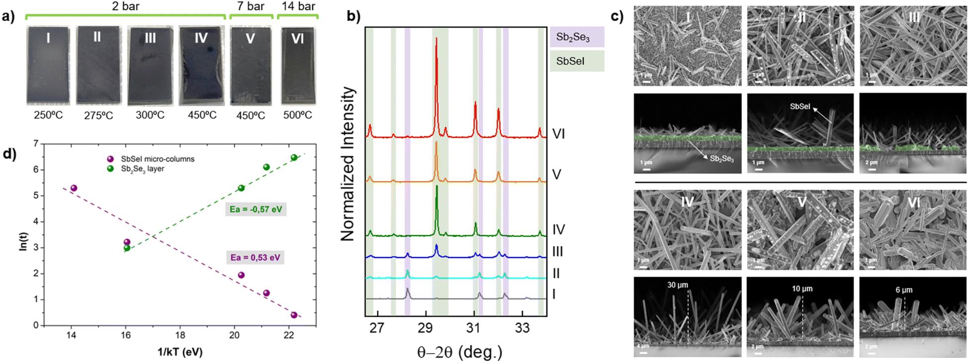 | ||
| Fig. 2 (a) Image of 2 × 1 cm SLG/Mo/SbSeI samples prepared under different annealing conditions. (b) X-ray diffractograms of the SLG/Mo/SbSeI series. Shaded areas indicate the 2θ reflections of Sb2Se3 (JCPDS-00-015-0861) and SbSeI (JCPDS-01-076-1354). (c) Top-view and cross-sectional SEM images of the SLG/Mo/SbSeI series. (d) Logarithm of the height and thickness (t) of SbSI micro-columns and Sb2Se3 layer respectively, as a function of the inverse of annealing temperature (1/kT). | ||
In addition to the SbSeI micro-columns, cross-sectional SEM images also show an unreacted Sb2Se3 layer, with a clearly defined structure for the low temperature treatments (I and II), whose thickness and uniformity decreases sequentially as the annealing temperature increases. At 450 °C no remains of this layer can be distinctly identified – except for sample VI, which presents a small characteristic Sb2Se3 peak, indicating that at higher pressures the 15 min annealing might not be enough to complete the reaction. On the other hand, the height and density of the micro-columnar structures increases with the annealing temperature, resulting in columns as large as 30 μm, and 1 μm thick approximately (IV). Alternatively, expanding the pressure to 7 and 14 bar, the height of the micro-columns decreases, but their width increases, see Fig. 2c (samples V and VI). It is thus demonstrated that the morphology of SbSeI samples can be tuned by precisely modifying the annealing conditions, such as coordinately varying temperature and pressure. All these results also suggest that the SbSeI formation and Sb2Se3 consumption are intimately linked processes, and that the transformation to SbSeI occurs sequentially as SbI3 vapor reacts with successive Sb2Se3 layers. Fig. 2d shows a linearization of the height of the micro-columns (purple line) and thickness of the unreacted Sb2Se3 layer (green line) as a function of the annealing temperature (for this plot, we have used values extracted from the SEM micrographs of samples I, II, III and IV). Interestingly, the activation energy Ea of both processes (extracted from the Arrhenius equation) is very similar, suggesting that they are indeed closely correlated. Moreover, the low value, ca. 0.50 eV, indicates that the conversion to SbSeI is a highly favourable chemical transformation.
Finally, TGA measurements were performed to determine precisely the reaction involved in the SbSeI formation. Considering that Sb2Se3 has a melting point of 611 °C (higher than any temperature used in this work), thermogravimetric analyses of SbI3 and SbSeI were carried out, see Fig. 3. Importantly, SbI3 presents a single weight loss process, which corresponds to the sublimation of the whole initial mass at 200 °C. Therefore, the reaction involves SbI3 vapor and Sb2Se3, rather than SbI3 decomposing into I2. Conversely, SbSeI decomposes at 300 °C, most likely into the binary compounds, since the TGA weight losses correspond accurately to the equivalent amounts of SbI3 and Sb2Se3. Also, the SbI3–Sb2Se3 phase diagram shows no stable stoichiometric phases aside from SbSeI and the binaries.32 Thus, it is reasonable to assume that the formation of the chalcohalide involves one mole of SbI3 and Sb2Se3 each, to form three moles of SbSeI, in accordance with eqn (1). This mechanism is consistent with the experiment shown in Fig. 2, where a direct correlation is observed between Sb2Se3 consumption and the formation of SbSeI as temperature increases, starting above 200 °C, upon which SbI3 sublimates, setting off the topologic transformation of the Sb2Se3 layer into SbSeI.
| SbI3 + Sb2Se3 → 3 SbSeI | (1) |
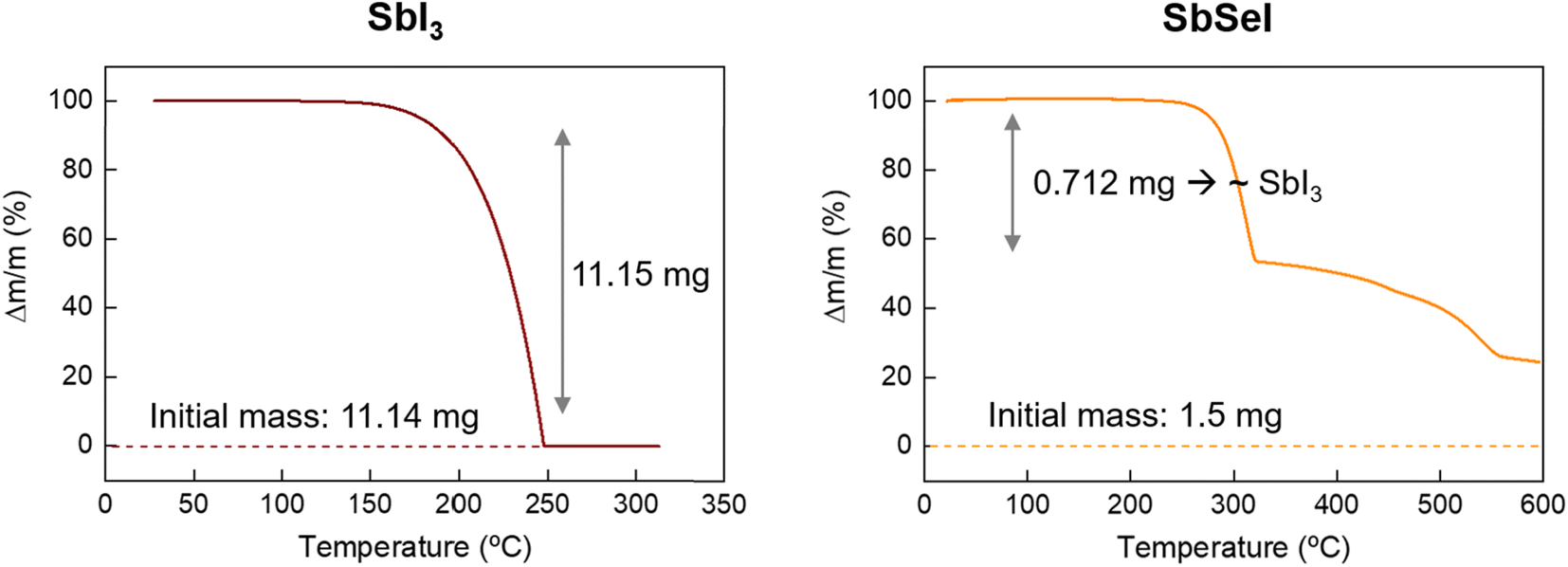 | ||
| Fig. 3 Thermogravimetric analysis curves of SbI3 and SbSeI. | ||
Structural and compositional characterization
The crystalline structure of SbSeI crystals (obtained from a sample synthesised at 450 °C and 2 bar) was studied by PXRD analysis in transmission mode. The crystal structure of SbSeI was stablished from single-crystal analysis in the early 1980s at room temperature. SbSeI crystallizes in orthorhombic cell, space group Pnma and volume 374.20 Å3 with Z = 4, which is maintained until 40 K.33 Accordingly, our measured spectrum was refined in the standard group Pnma, and the atomic coordinates obtained from the former study were used as starting values for the Rietveld analysis. The final refined pattern is depicted in Fig. 4a together with the experimental and refined pattern difference. The obtained cell parameters, a = 8.71154(0.00031) Å, b = 4.13299(0.00019) Å, c = 10.42534(0.00043) Å and V = 375.362(0.027) Å3 match well with those obtained by the single-crystal. Consequently, the unit cell structure was obtained and represented with VESTA software, see Fig. 4b.34 Note that the material forms covalently-bonded chains or ribbons along the b direction, resulting in an anisotropic low-dimensional (quasi-1D) crystalline structure.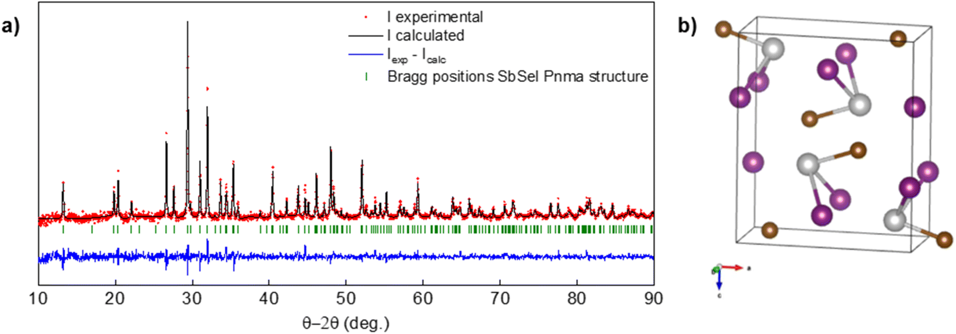 | ||
| Fig. 4 (a) Experimental (red points) and Rietveld (black) refined patterns, along with the difference profile (blue curve) and Bragg reflections (green sticks) of SbSeI crystalline powder. (b) SbSeI unit cell structure obtained from XRD analysis, represented with the VESTA software: grey – Sb, brown – Se, purple – I. | ||
HR-TEM-EDX analyses have been performed on a lamella obtained from an SbSeI sample prepared at 450 °C and 2 bar (similar to sample IV in Fig. 2a). The lamella (preparation process described in the Experimental procedure section and shown in Fig. S1†) has been expressly manipulated to include a longitudinal section of a micro-column and several cross-sectional cuts, see Fig. 5a – i.e. there is one column lying down as well as other ones passing through the lamella. Fig. 5b presents the HR-TEM image corresponding to an area inside the red square in Fig. 5a, confirming that SbSeI micro-columnar structures are indeed constituted by a continuous crystalline layer extending through several microns, with no evidence of grain boundaries or structural defects, therefore suggesting that they are formed by single crystals (Fig. S3† includes other TEM images with different magnification). Note that the black markings which can be seen in some images correspond to different orientations of the crystal, possibly due to undulations of the crystal occurred during the lamella preparation, and not to grain boundaries, which would appear as clear changes in the direction of the interference fringes. Fig. 5c shows the fast Fourier transform of the image Fig. 5b, representing the theoretical electron diffraction pattern, which can be identified as those of an orthorhombic structure on the [001] zone axis, in which 〈200〉, 〈220〉 and 〈020〉 are clearly indexed, confirming the structure determined by PXRD. Finally, EDX profile analysis has been performed on one of the transversally cut columns (Fig. 5d), revealing a very uniform composition with minimal variations in the relative atomic amounts of Sb, Se and I, which correspond to approximately one third each, as expected of SbSeI (36%, 33% and 31% respectively), see the profile map in Fig. 5e. Interestingly, a slight increase in the Se content is found on the column's surface, which might indicate the presence of elemental Se as an amorphous secondary phase, since it was not detected by PXRD. In addition, other areas of the lamella have been analysed, including the longitudinally cut column, showing a similar distribution, see Fig. S4.† Curiously, Fig. S4d† shows a very significant increase in Se amount along the Mo interface, which could result from a small amount of unreacted Sb2Se3, or the presence of a MoSe2 layer, which is known to form spontaneously during annealing under Se atmosphere.35
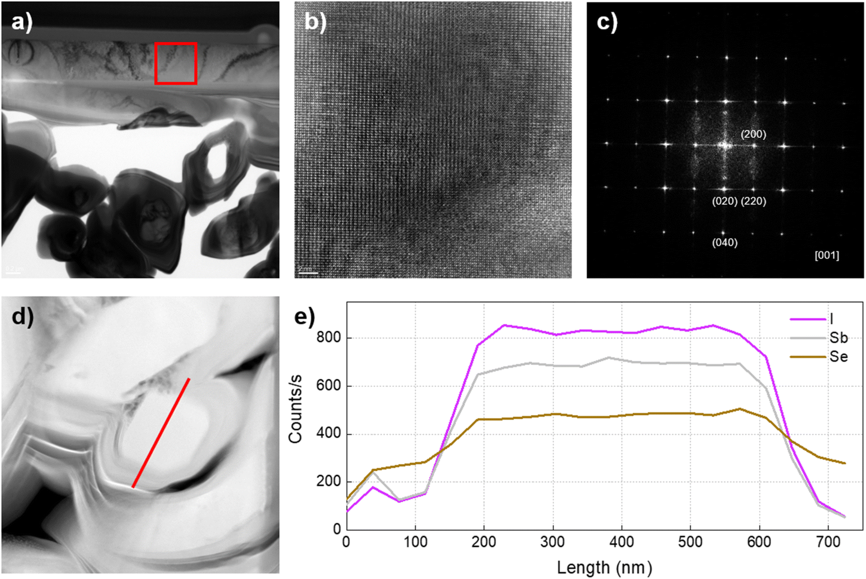 | ||
| Fig. 5 TEM and EDX analysis of a Mo/SbSeI sample prepared at 450 °C and 2 bar. (a) [001] HR-TEM cross-sectional image in the region marked with a red square. (b) HR-TEM image with high magnification. (c) FFT of image (b). (d) Cross-sectional image of an SbSeI column severed transversally. (e) EDX profile mapping of the column in (d) along the red line. | ||
Similar TEM-EDX analyses have also been performed on samples prepared at 450 °C and 7 bar, and 275 °C and 2 bar (equivalent to V and II, respectively). For the 450 °C and 7 bar sample, analogous results from those in Fig. 5 are observed, revealing an excellent crystallinity and uniform composition, see Fig. S5.† Nonetheless, for the 275 °C and 2 bar sample, no integer SbSeI micro-column has been successfully preserved in the lamella – instead, we observe a polycrystalline layer of unreacted Sb2Se3, see Fig. S6.† Note in Fig. S6c–e† that, in this case, grain boundaries of Sb2Se3 can be clearly identified as regions where the interference fringes present an abrupt pattern discontinuity.
The performed structural and compositional analyses clearly demonstrate that the transformation of a Sb2Se3 layer to SbSeI micro-columnar structure is a highly favourable process, and that the amount of transformed material depends largely on the synthesis conditions. In particular, selectively adjusting temperature and pressure allows to tune the morphology, crystallinity and purity of the SbSeI phase. Furthermore, using a high pressure-based synthesis procedure has been shown to be crucial to avoid iodine loss and to refine the annealing conditions to develop a systematic method to fabricate samples with reproducible features.
Electronic and optoelectronic characterization
One of the main motivations to develop chalcohalide materials by vacuum-based techniques is to use their electronic properties for applications such as photovoltaics or electro-photocatalysis. To achieve this goal, it is necessary to develop devices that allow an efficient separation and extraction of photo-generated carriers, using electron and hole transport layers for optimum selectivity of each. To build a suitable architecture of layers, considerations such as band alignment, conduction type, or chemical compatibility can either boost or kill the optoelectronic performance of the device. Therefore, studying the properties of the absorber alone can be very helpful to make an educated choice of the complementary layers. Also, given the atypical columnar morphology of SbSeI samples, we believe that characterizing single crystals (i.e. micro-columns) will shed additional light on their properties and potential.In order to perform specific electrical characterization on individual micro-columns, a sample of pure SbSeI on glass/Mo was exfoliated with the help of a PDMS stamp, resulting in a non-uniform coverage of the PDMS surface. Then, the PDMS stamp was used to transfer the SbSeI structures to a Si/SiO2 substrate with prepatterned Au and Pt contacts. Observe in Fig. 6a that the columnar crystals are scattered all over the SiO2 and metallic surfaces. Note however that in the red circled areas there are individual columns bridging between adjacent contacts, which allows to perform I–V measurements, applying a voltage sweep with and without illumination, see insets in Fig. 6b. To correctly interpret these results, it is required to understand precisely why p or n-type semiconductors conduct differently when they are contacted with metals of different work function, such as gold and platinum. The discussion is presented in the ESI, see Annex 1.†
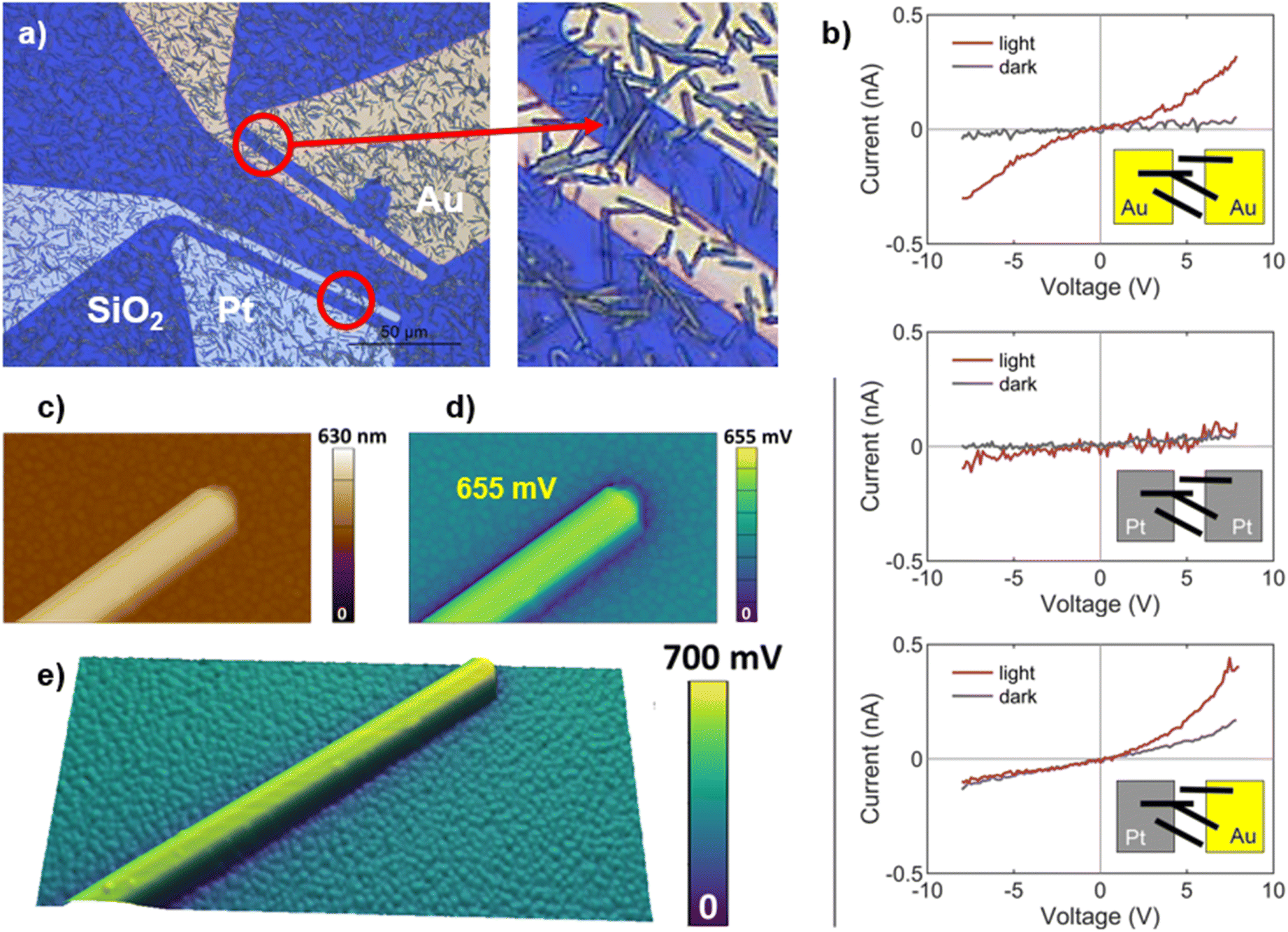 | ||
| Fig. 6 (a) Optical microscope image of SbSeI crystals deposited on a Si/SiO2 substrate with prepatterned Au and Pt contacts. (b) J–V measurements performed on a SbSeI micro-column connected to metal contacts by Schottky barrier. The following metals have been used: Au contacts, Pt contacts, Au and Pt contacts (Au as source). (c) and (d) show the topographical and surface potential map of a micro-column lying on a polycrystalline gold surface. The color scale reflects the difference of SP respect to the surrounding gold surface. (e) KPFM image – corresponds to surface potential colour map overlapped with height topology image. Height of the column is 787 nm and the SP 700 mV. | ||
By I–V measurements, it is observed that SbSeI micro-columns present a clear diode response when combined with Au contacts, which is further enhanced under illumination (Fig. 6a). On the other hand, Pt electrodes lead to a significantly reduced performance, both under dark and light conditions. Besides, the signal to noise ratio in the latter case is very low, making it difficult to distinguish whether the observed variations are due to diode behaviour or instrumental noise (Fig. 6b). Indeed, note that when applying 5 V, the measured current with Au is several times higher than Pt. This is consistent with Schottky barriers forming at the micro-column/metal interfaces, that are higher in the case of Pt than in the case of Au. Considering that Au has a work function of 5.1 eV, while Pt's is higher at 6.4 eV, and according to the discussion in the ESI (Annex 1),† these results indicate that SbSeI could be an n-type semiconductor. Otherwise, keep in mind that the measurements here presented should not be interpreted as the actual photovoltaic performance of chalcohalide materials, since they are not based on any optimized device architecture, instead corresponding to metal–semiconductor junctions.
I–V measurements have also been performed connecting each end of an SbSeI micro-column with a different metal – Au as the source electrode and Pt as the drain. Using this configuration, the system also shows a diode response, with higher current under illumination conditions, see Fig. 6b (third inset). Remarkably, the fact that I–V curves have been obtained using the Au–Pt contacts can also be explained by our hypothesis that SbSeI is an n-type material, since electron conduction should not be hampered by any energy barrier in this configuration (see Annex 1†).
In addition to current–voltage measurements, the work function of SbSeI crystals was also studied by Kelvin probe force microscopy (KPFM). In this case, a micro-manipulator was used to select individual crystals from a sample prepared at 450 °C, and then placed on a polycrystalline Au film. As described in the Experimental procedure section, for the setup employed, higher (lower) SP corresponds to lower (higher) surface work function (ϕ). The Fig. 6c shows the topographical image of a micro-column lying-down on the surface, displaying a height of 630 nm. The surface potential map (Fig. 6d) indicates that its surface potential is higher than that of the surrounding surface by 650 mV. Hence, considering the polycrystalline gold as a reference for the work function with a value of 4.9 eV,36 the work function of the of SbSeI microcrystals can be estimated at ∼4.25 eV. By measuring several micro-columns, we found a variation in the SP values ranging in ∼150 mV. The 3D image in the Fig. 6e provides a 3D visualization of another micro-column, where the surface potential variation is overlaid with the topography. Interestingly, the fact that the work function of SbSeI is lower than that of gold may be due to the material being an n-type semiconductor, in line with the discussion above.
As additional evidence of the suggested n-type behaviour, the valence band has been determined by X-ray photoemission spectroscopy (XPS), see Fig. S7.† Considering that the bandgap of SbSeI material is approximately 1.7 eV, and the measured valence band energy is −1.04 eV with respect to the Fermi level, these results imply that the Fermi level is slightly closer to the conduction band (see the energy diagram in Fig. S7b†), suggesting that SbSeI might be indeed an n-type semiconductor. Nevertheless, this hypothesis needs further validation by conductivity or capacitance measurements, such as Hall effect characterization or the Seebeck coefficient.37
Finally, solar cell prototypes have been prepared using the SLG/Mo/SbSeI/CdS/intrinsic-ZnO/ITO/Ag structure, where CdS acts as ETL. Different conditions have been considered for SbSeI synthesis: 300 °C at 2 bar, and 275 °C at 2 bar. Due to the complicated columnar morphology of SbSeI samples, different individual cells yielded a wide dispersion of results. Thus, for simplicity, we present the average and maximum values in Fig. 7a and b (see Fig. S8† for the complete set of results). For the 275 °C sample, efficiency of 0.8% is obtained with average Voc values of 350 mV. Nevertheless, from the double hump-like EQE curve it is clear that a lower bandgap material (Eg ∼ 1.25 eV) and a wider bandgap material (Eg ∼ 1.6–1.7 eV) are contributing to the current generation (see Fig. 7c), in line with the SEM and PXRD analyses where coexistence of SbSeI and Sb2Se3 was found for the samples prepared at annealing temperatures below 300 °C (Fig. 2b and c). On the other hand, samples annealed at 300 °C show impressive Voc values up to 560 mV, which are amongst the highest reported for SbSeI with any synthesis process. However, a very low Jsc (1.9 mA cm−2 mean) leads to efficiencies around 0.3% – which nonetheless corresponds to a record efficiency for substrate Mo/SbSeI/CdS-based device, to the best of our knowledge –, suggesting that the solar cell might be limited by poor carrier collection. In this case, a bandgap of 1.78 eV has been extracted from the EQE curve, confirming that the chalcohalide is the dominant phase. The bandgap has also been confirmed from the absorption spectra by photothermal deflection spectroscopy (PDS), which has been fitted with the Tauc–Urbach model to obtain a direct bandgap of 1.74 eV, see spectra in Fig. S9.†38
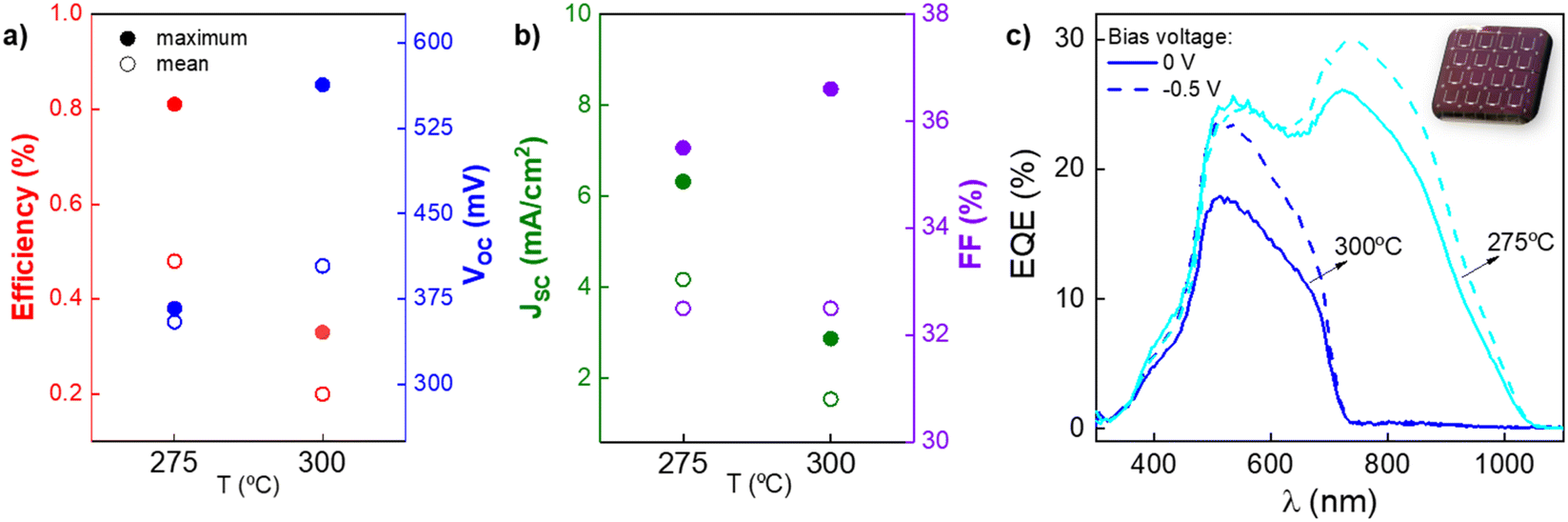 | ||
| Fig. 7 Optoelectronic parameters of MoSbSeI/CdS/i-ZnO/ITO solar cells under different annealing conditions: (a) PCE and Voc, (b) Jsc and FF, (c) EQE (with applied 0 V and −0.5 V). | ||
As seen in the SEM images (Fig. 2c), the columnar morphology causes that in many regions there is no phase continuity, which could lead to situations where the CdS is in direct exposure with the Mo back contact. Also, chemical bath deposition is not a conformal technique, thus it cannot be ruled out that a partial CdS coverage may lead to a poor contact, physically isolating some parts of the cell from the short circuit, this possibly being at the origin of a deficient carrier collection and extremely low Jsc. This effect could also be the cause of the broad dispersion of optoelectronic parameters, since different regions of the sample (i.e. different cells) may have fluctuating density and orientation of the micro-columnar structures.
Moreover, although this architecture has been previously implemented with SbSeI for investigating its PV performance, possibly due to its good matching with similar quasi-1D materials such as Sb2(S,Se)3 or Sb2Se3, it might not be entirely suitable for chalcohalides. Indeed, unlike SbSeI, Sb chalcogenides are typically accepted as p-type semiconductors, and they have lower bandgap (between 1.2 and 1.6 eV). Therefore, neither the carrier transport layers have been optimized for this n-type semiconductor, nor is the band alignment optimal, as SbSeI has a larger bandgap. Despite these important drawbacks, PV effect has been consistently observed with Voc higher than most quasi-1D semiconductors, proving the potential of SbSeI to build efficient and versatile solar cell thin films, provided that a suitable device architecture will be developed.
SbSeBr: Results and discussion
In addition to the synthesis and characterization of SbSeI micro-columnar samples, SLG/Mo/SbSeBr have also been prepared in accordance with the procedure described in the Experimental procedure section. Following an optimization study, testing the process under different conditions of temperature and pressure, it was determined that the optimal conditions to obtain SbSeBr are 300 °C at 4 bar. Note in Fig. 8a that the PXRD pattern has been indexed according to an orthorhombic structure (space group Pnma) compatible with SbSeBr, being this structure equivalent to that of SbSeI. A spurious Bragg reflection to the chalcohalide phase has been detected at 29° (the peak at 40.5° belongs to the Mo substrate), which may correspond to metallic Sb. This can be expected to a certain extent, since in the current synthesis conditions, Sb2Se3 is used as a precursor and SbBr3 in excess. SEM images also show the formation of anisotropic columnar-like structures, although the sample presents a more compact morphology, see Fig. 8b. This may be due to the fact that the electronegativity difference between halide and Sb is larger with Br, resulting in a less anisotropic structure (as explained above, experimental evidence indicates that the quasi-1D nature of van der Waals materials is connected to presenting a small difference in electronegativity between cation and anions). Moreover, crystals are smaller and tend to grow parallel to the substrate. Importantly, these results represent one of the first successful attempts to fabricate SbSeBr thin films. So far, chemical routes have not been favourable due to the lower dissociative capacity of SbBr3 in polar solvents such as DMF, and its low melting point (96.6 °C), which makes it difficult to find suitable conditions to synthesise the chalcohalide without loss of bromide. In this regard, working under a controlled environment by our high-pressure method has proven to be especially effective.39,40 Additional research is required to further understand the formation mechanism and to explore the possibilities of tuning the morphology.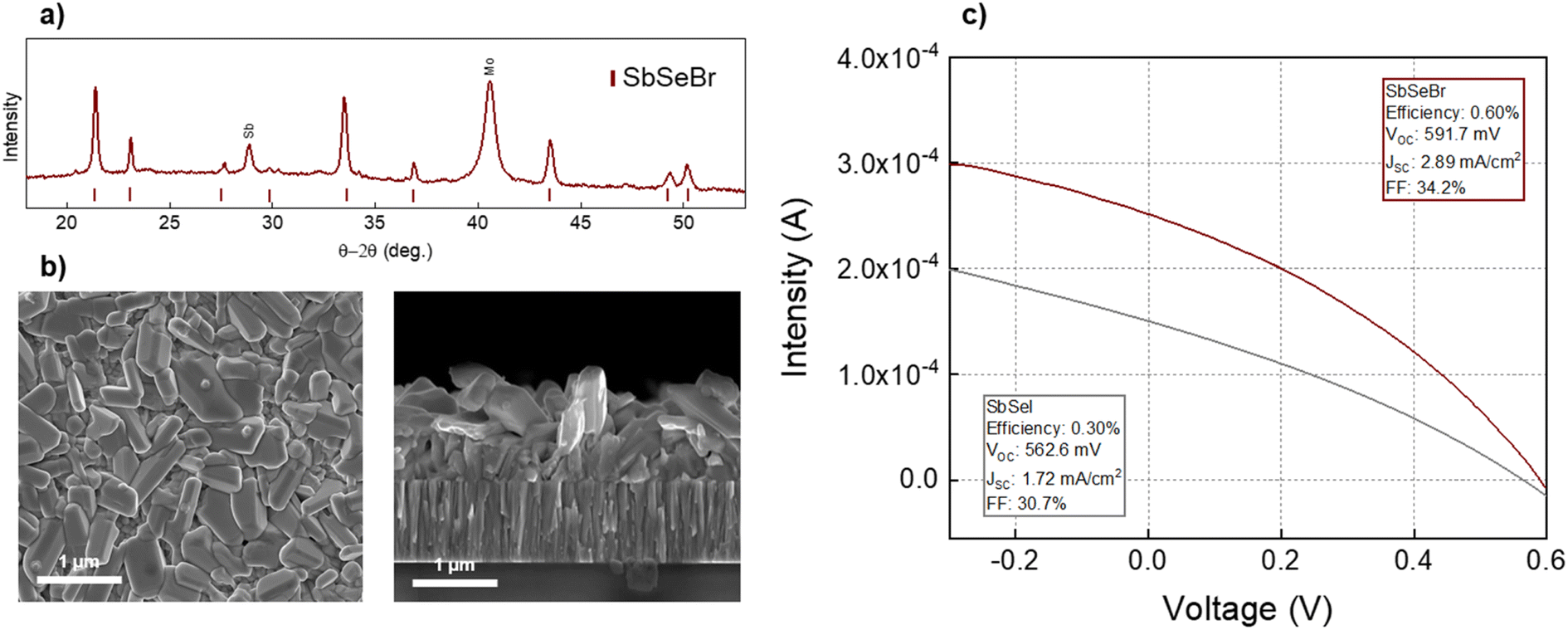 | ||
| Fig. 8 (a) XRD pattern of the SLG/Mo/SbSeBr sample, (b) SEM top-view and cross-section micrographs of the SLG/Mo/SbSeBr sample, (c) intensity–voltage curves of SbSeBr and SbSeI prototype solar cells. | ||
Finally, a solar cell prototype has been prepared using the SLG/Mo/SbSeBr/CdS/intrinsic-ZnO/ITO/Ag structure. Significantly, high Voc values up to 600 mV have been obtained with efficiency of 0.6% (the highest reported, to the best of our knowledge). Nevertheless, a very low Jsc is still the main limitation of the device, in line with results from SbSeI above, which can be attributed to a poor carrier collection (deficient contact or inadequate band structure). Still, the J–V curve of SbSeBr presents improvements with respect to SbSeI, likely due to the more benign morphology of the former, see Fig. 8c. Overall, these results demonstrate that the high-pressure synthesis methodology presented in this work opens the door to the fabrication of a large family of chalcohalide materials whose formula is MCX – M = metal (Sb, Bi), C = chalcogen, X = halogen. Likewise, preliminary results of optoelectronic properties for SbSeI and SbSeBr show a high Voc and photoactive response, demonstrating their potential for photovoltaic applications.
Conclusions
This work presents the first successful attempt to synthesise SbSeX (X = I, Br) micro-columnar samples by a high-pressure PVD-based methodology. By working at pressures above 1 atm, a new synthesis variable has been introduced, through which it is possible to constrain the evaporation rate of halide reagents, avoiding the decomposition and re-evaporation of volatile compounds. Likewise, it has been shown that the coordinated variation of temperature, pressure and annealing time allows to tune the morphology and structure of SbSeX crystals, achieving variances of the order of several microns in the length and thickness of these crystals. Significantly, by this method it has been possible to prepare SbSeI samples (which had previously been synthesised by chemical routes), showing high crystalline quality, outstanding compositional uniformity, and phase purity. Also, we have successfully obtained SbSeBr polycrystalline layers with stable structure and composition. Through an in-depth study of the structure as a function of annealing time and T, as well as thermogravimetric analyses, it has been shown that the material is formed by a reaction between SbX3 and Sb2Se3, resulting in 3 moles of SbSeX. For this work, a strategy has also been designed to study the electronic properties of chalcohalide micro-devices, based on SbSeI single crystals contacted with metals of different work function. Thereby, it has been demonstrated that micro-scale devices with Au electrodes present a clear diode response, which is enhanced under illumination, suggesting that the semiconductor could be n-type. This hypothesis is supported by KPFM measurements, showing that SbSeI has lower work function than that of Au. However, more characterization is needed to validate the hypothesis. Finally, prototype solar cells have yielded large Voc around 600 mV, among the highest reported for this family of materials, although the low conversion efficiency may result from a poor contact with the ETL, and inefficient band structure. Despite this circumstance, the high Voc, evidence of photoactivity, and the SbSeBr results (being the first results of PV activity in this material, to the best of our knowledge), show the potential of these materials as high-performance crystalline semiconductors with interest for applications in energy and electronics.Author contributions
Ivan Caño: writing – original draft, methodology, investigation, formal analysis, conceptualization. Alejandro Navarro: methodology, investigation. Edoardo Maggi: methodology, investigation. Maria Barrio: investigation (PXRD measurements). Josep Lluís Tamarit: investigation (TG measurements), writing – review and editing. Simon Svatek & Elisa Antolín: investigation, formal analysis (micro-scale devices). Shunya Yan & Esther Barrena: investigation, formal analysis (KPFM measurements). Beatriz Galiana: formal analysis (HR-TEM analysis). Marcel Placidi: writing – review and editing, funding acquisition, supervision. Joaquim Puigdollers: resources, funding acquisition. Edgardo Saucedo: writing – review and editing, methodology, conceptualization, validation, resources, funding acquisition, supervision.Conflicts of interest
There are no conflicts to declare.Acknowledgements
This research has received funding from the European Union H2020 Framework Program under through the SENSATE project: Low dimensional semiconductors for optically tunable solar harvesters (grant agreement number 866018). Other funding from the Ministry of Science and Innovation of the Government of Spain under the MATER-ONE (PID2020-116719RB-C41) and MIRACLE projects. I. C. acknowledges UPC and Banco Santander for his FPI-UPC PhD scholarship. A. N. acknowledges the acknowledges the Ministry of Science and Innovation for his FPI PhD scholarship. E. B. acknowledges node DME (Cadiz, Spain) of ICTS “ELECMI”. M. P. acknowledges the financial support from Ministry of Science and Innovation within the Ramon y Cajal program (RYC-2017-23758). E. S. acknowledges the ICREA Academia program.References
- R. N. Bhattacharya and P. Pramanik, Sol. Energy Mater., 1982, 6, 317–322 CrossRef CAS.
- A. Mavlonov, T. Razykov, F. Raziq, J. Gan, J. Chantana, Y. Kawano, T. Nishimura, H. Wei, A. Zakutayev, T. Minemoto, X. Zu, S. Li and L. Qiao, Sol. Energy, 2020, 201, 227–246 CrossRef CAS.
- S. Messina, M. T. S. Nair and P. K. Nair, J. Electrochem. Soc., 2009, 156, H327 CrossRef CAS.
- Z. Duan, X. Liang, Y. Feng, H. Ma, B. Liang, Y. Wang, S. Luo, S. Wang, R. E. I. Schropp, Y. Mai and Z. Li, Adv. Mater., 2022, 34, 2202969 CrossRef CAS.
- Y. Zhao, S. Wang, C. Jiang, C. Li, P. Xiao, R. Tang, J. Gong, G. Chen, T. Chen, J. Li and X. Xiao, Adv. Energy Mater., 2022, 12, 2103015 CrossRef CAS.
- Y. Zhou, L. Wang, S. Chen, S. Qin, X. Liu, J. Chen, D. J. Xue, M. Luo, Y. Cao, Y. Cheng, E. H. Sargent and J. Tang, Nat. Photonics, 2015, 9, 409–415 CrossRef CAS.
- I. Caño, P. Vidal-Fuentes, A. G. Medaille, Z. Jehl, A. Jiménez-Arguijo, M. Guc, V. Izquierdo-Roca, C. Malerba, M. Valentini, M. Jiménez-Guerra, M. Placidi, J. Puigdollers and E. Saucedo, Sol. Energy Mater. Sol. Cells, 2023, 251, 112150 CrossRef.
- T. P. Weiss, P. Arnou, M. Melchiorre, M. Guennou, D. Siopa, C. Pauly, I. Peral Alonso, P. J. Dale and S. Siebentritt, Phys. Rev. Appl., 2020, 14, 1–11 Search PubMed.
- K. T. Butler, S. McKechnie, P. Azarhoosh, M. Van Schilfgaarde, D. O. Scanlon and A. Walsh, Appl. Phys. Lett., 2016, 108, 112103 CrossRef.
- B. Peng, K. Xu, H. Zhang, Z. Ning, H. Shao, G. Ni, J. Li, Y. Zhu, H. Zhu and C. M. Soukoulis, Adv. Theory Simul., 2018, 1, 1700005 CrossRef.
- K. T. Butler, J. M. Frost and A. Walsh, Energy Environ. Sci., 2015, 8, 838–848 RSC.
- E. Fatuzzo, G. Harbeke, W. J. Merz, R. Nitsche, H. Roetschi and N. Ruppet, Phys. Rev., 1962, 127, 2036 CrossRef CAS.
- M. Coll, J. Gazquez, I. Fina, Z. Khayat, A. Quindeau, M. Alexe, M. Varela, S. Trolier-Mckinstry, X. Obradors and T. Puig, Chem. Mater., 2015, 27, 6322–6328 CrossRef CAS.
- W. Koch, R. Munser, W. Ruppel and P. Wurfel, Solid State Commun., 1975, 17, 847–850 CrossRef CAS.
- R. E. Brandt, V. Stevanović, D. S. Ginley and T. Buonassisi, MRS Commun., 2015, 5, 265–275 CrossRef CAS.
- R. C. Kurchin, P. Gorai, T. Buonassisi and V. Stevanović, Chem. Mater., 2018, 30, 5583–5592 CrossRef CAS.
- B. Toroń, K. Mistewicz, M. Jesionek, M. Kozioł, M. Zubko and D. Stróż, Energy, 2022, 238, 122048 CrossRef.
- Y. C. Choi and K. W. Jung, Nanomaterials, 2021, 11, 3206 CrossRef CAS.
- K. W. Jung and Y. C. Choi, ACS Appl. Energy Mater., 2021, 5, 5348–5355 CrossRef.
- R. Nie, M. Hu, A. M. Risqi, Z. Li and S. Il Seok, Adv. Sci., 2021, 8, 2003172 CrossRef CAS.
- S. K. Balakrishnan, P. C. Parambil and E. Edri, Chem. Mater., 2022, 34, 3468–3478 CrossRef CAS.
- C. Jiang, J. Zhou, R. Tang, W. Lian, X. Wang, X. Lei, H. Zeng, C. Zhu, W. Tang and T. Chen, Energy Environ. Sci., 2021, 14, 359–364 RSC.
- C. L. Yaws, The Yaws Handbook of Vapor Pressure Antoine Coefficients 2nd edn, 2015 Search PubMed.
- Z. Ran, X. Wang, Y. Li, D. Yang, X. G. Zhao, K. Biswas, D. J. Singh and L. Zhang, npj Comput. Mater., 2018, 4(14) DOI:10.1038/s41524-018-0071-1.
- J. F. Alward, C. Y. Fong, M. El-Batanouny and F. Wooten, Solid State Commun., 1978, 25, 307–310 CrossRef CAS.
- S. A. Park, M. Y. Kim, J. Y. Lim, B. S. Park, J. D. Koh and W. T. Kim, Phys. Status Solidi B, 1995, 187, 253–260 CrossRef CAS.
- Z. Li, X. Liang, G. Li, H. Liu, H. Zhang, J. Guo, J. Chen, K. Shen, X. San, W. Yu, R. E. I. Schropp and Y. Mai, Nat. Commun., 2019, 10, 1–9 CrossRef.
- K. Yang, B. Li and G. Zeng, Superlattices Microstruct., 2020, 145, 106618 CrossRef CAS.
- P. Vidal-Fuentes, M. Placidi, Y. Sánchez, I. Becerril-Romero, J. Andrade-Arvizu, Z. Jehl, A. Pérez-Rodríguez, V. Izquierdo-Roca and E. Saucedo, Sol. RRL, 2020, 4, 1–11 Search PubMed.
- J. Rodríguez-Carvajal, T. Roisnel and J. Gonzales-Platas, Laboratoire Léon Brillouin CEA-CNRS, CEN Saclay, France, 2005 Search PubMed.
- F. Palazon, Sol. RRL, 2022, 6, 2100829 CrossRef CAS.
- Z. S. Aliev, S. S. Musaeva, D. M. Babanly, A. V. Shevelkov and M. B. Babanly, J. Alloys Compd., 2010, 505, 450–455 CrossRef CAS.
- G. P. Voutsas and P. J. Rentzeperis, Z. Kristallogr., 1982, 161, 111–118 CrossRef CAS.
- K. Momma and F. Izumi, J. Appl. Crystallogr., 2011, 44, 1272–1276 CrossRef CAS.
- I. Caño, P. Vidal-Fuentes, L. Calvo-Barrio, X. Alcobé, J. M. Asensi, S. Giraldo, Y. Sánchez, Z. Jehl, M. Placidi, J. Puigdollers, V. Izquierdo-Roca and E. Saucedo, ACS Appl. Mater. Interfaces, 2022, 14, 11222–11234 CrossRef PubMed.
- H. Kawano, Prog. Surf. Sci., 2022, 97, 100583 CrossRef CAS.
- T. D. C. Hobson, L. J. Phillips, O. S. Hutter, H. Shiel, J. E. N. Swallow, C. N. Savory, P. K. Nayak, S. Mariotti, B. Das, L. Bowen, L. A. H. Jones, T. J. Featherstone, M. J. Smiles, M. A. Farnworth, G. Zoppi, P. K. Thakur, T. L. Lee, H. J. Snaith, C. Leighton, D. O. Scanlon, V. R. Dhanak, K. Durose, T. D. Veal and J. D. Major, Chem. Mater., 2020, 32, 2621–2630 CrossRef CAS.
- A. J. Lopez-Garcia, C. Voz, J. M. Asensi, J. Puigdollers, V. Izquierdo-Roca and A. Pérez-Rodríguez, Sol. RRL, 2023, 7, 2200928 CrossRef CAS.
- S. K. Balakrishnan, P. C. Parambil and E. Edri, Chem. Mater., 2022, 34, 3468–3478 CrossRef CAS.
- C. Airoldi, P. L. O. Volpe and J. M. M. de M. Lira, Polyhedron, 1983, 2, 1125–1129 CrossRef CAS.
Footnote |
| † Electronic supplementary information (ESI) available. See DOI: https://doi.org/10.1039/d3ta03179a |
| This journal is © The Royal Society of Chemistry 2023 |