
Critical role of 1D materials in realizing efficient and stable perovskite solar cells
Yu
Chen†
a,
Baibai
Liu†
a,
Qian
Zhou
a,
Danqing
Ma
a,
Xiao
Han
a,
Dongmei
He
*a,
Shi
Chen
 *b,
Yuelong
Li
c,
Shirong
Lu
d,
Zong-Xiang
Xu
e,
Cong
Chen
*f,
Hua
Yu
*a and
Jiangzhao
Chen
*ag
*b,
Yuelong
Li
c,
Shirong
Lu
d,
Zong-Xiang
Xu
e,
Cong
Chen
*f,
Hua
Yu
*a and
Jiangzhao
Chen
*ag
aKey Laboratory of Optoelectronic Technology & Systems (Ministry of Education), College of Optoelectronic Engineering, Chongqing University, Chongqing 400044, China. E-mail: hedongmei@cqu.edu.cn; yuhua@cqu.edu.cn; jiangzhaochen@cqu.edu.cn
bJoint Key Laboratory of the Ministry of Education, Institute of Applied Physics and Materials Engineering, University of Macau, Avenida da Universidade, Taipa, Macau 999078, China. E-mail: shichen@um.edu.mo
cInstitute of Photoelectronic Thin Film Devices and Technology of Nankai University, Key Laboratory of Photoelectronic Thin Film Devices and Technology of Tianjin, Solar Energy Research Center of Nankai University, Tianjin 300350, China
dDepartment of Material Science and Technology, Taizhou University, Taizhou 318000, China
eDepartment of Chemistry, Southern University of Science and Technology, Shenzhen 518055, China
fState Key Laboratory of Reliability and Intelligence of Electrical Equipment, School of Materials Science and Engineering, Hebei University of Technology, Tianjin 300401, China. E-mail: chencong@hebut.edu.cn
gFaculty of Materials Science and Engineering, Kunming University of Science and Technology, Kunming 650093, China
First published on 17th August 2023
Abstract
Perovskite solar cells (PSCs) have obtained great triumph in photovoltaic technologies due to their excellent optoelectronic properties. In particular, the use of one-dimensional (1D) materials including 1D perovskites (defined according to crystal structures) and 1D carrier transport materials (defined according to morphology) has been widely demonstrated to be able to effectively enhance the power conversion efficiency (PCE) and stability of PSCs because of their some unique properties. In view of the huge contributions of 1D materials in PSCs, a comprehensive understanding of 1D materials in PSCs is necessary. In this review, we first introduce the structure, properties, and synthesis of 1D perovskites. Then, we discuss the recent development of PSCs based on 1D/3D perovskite heterojunctions including bulk 1D/3D perovskite heterojunctions and interfacial 1D/3D perovskite heterojunctions. Subsequently, we discuss the 1D carrier transport layers. Finally, we give a plausible conclusion and outlook of 1D materials in PSCs which can further facilitate the advancement of PSCs.
1. Introduction
Perovskite solar cells (PSCs) have become one of the most promising next-generation photovoltaic technologies owing to their brilliant optoelectronic properties including high light absorption coefficient, tunable bandgap, and small exciton binding energy.1–7 With the continuous efforts of scientists, the power conversion efficiency (PCE) was boosted from 3.9% to 25.8% in the past ten years.8,9 Thus, the development of PSCs is of significant importance for photovoltaic technologies and green energy.The single-junction PSCs are either a normal structure (n-i-p) or inverted structure (p-i-n), consisting of electrodes (transparent electrode and back electrode), carrier transport layers (electron transport layer (ETL) and hole transport layer (HTL)), and the perovskite absorber layer; the perovskite light-harvesting layer is sandwiched between the ETL and HTL. The quality of each layer is crucial for the overall performance and stability of PSCs. Among these layers, the preparation of high-quality perovskite layers is relatively difficult. Due to the rapid crystal growth process and ionic nature of perovskites, there are numerous defects at grain boundaries (GBs) and the surface of the perovskite film. These defects not only hinder carrier transport and cause nonradiative recombination but also are very sensitive to oxygen and water, which has a significant negative impact on the photovoltaic performance and stability of PSCs.10,11 Moreover, the mismatched thermal expansion coefficients between perovskite layers and carrier transport layers would lead to lattice distortion at grain boundaries, the residual lattice strain, and facilitated ion migration due to reduced ion migration activation energy, which is deleterious to the operational stability of PSCs.12–16 In addition to the perovskite layer, a suitable charge transport layer is also necessary. A suitable charge transport layer (CTL) should not only require efficient charge extraction and transport but also provide good substrates for perovskite crystallization and growth. Therefore, developing appropriate CTL materials to ameliorate the quality of the perovskite layer is necessary. In order to mitigate or overcome the above issues, various strategies have been developed, mainly including interface engineering,16–18 precursor and antisolvent engineering,19,20 additive engineering,21–24 perovskite grain engineering,25 composition engineering,25,26 dimensionality engineering,25,27,28 nonstoichiometric approach,25etc. Various materials with multiple functional groups have been employed through these strategies. Among them, low-dimensional (LD) perovskite materials such as zero-dimensional (0D),29 one-dimensional (1D),29 and two-dimensional (2D)30–34 have drawn much attention because they usually exhibited better moisture stability than 3D perovskites. Except for intrinsic moisture stability, it was widely revealed that LD perovskites could effectively passivate the defects within 3D perovskites, suppress ion migration and mitigate residual strain at grain boundaries and interfaces.28,34–36 Although 0D and 2D perovskites have made great contributions, this review only focused on discussing the progress of 1D perovskites in PSCs. In addition to 1D perovskites (defined according to the crystal structure), 1D carrier transport layers (according to morphology) are also very attractive, which can not only provide a direct pathway for electron transport but also provide a porous network for better pore-filling of perovskites.37 Therefore, 1D materials play an important role in PSCs. In view of the huge contributions of 1D materials in PSCs, a comprehensive understanding of 1D materials in PSCs is necessary.
Although 1D materials have been frequently applied in PSCs and great progress has been obtained, there are few reviews concentrated on summarizing and discussing the development of 1D materials in PSCs.38–44 It is imperative to summarize the recent developments of this topic and provide meaningful insights for researchers. In this review, we first introduced the structure, properties, and synthesis of 1D perovskites. Then we discussed the recent development of PSCs based on 1D/3D perovskite heterojunctions including bulk 1D/3D perovskite heterojunctions and interfacial 1D/3D perovskite heterojunctions. Subsequently, we discussed the 1D carrier transport layers. Finally, we gave a plausible conclusion and outlook of 1D materials in PSCs that could improve future work in this field.
2. 1D perovskites
2.1 Structures and properties of 1D perovskites
For the organic–inorganic metal halide perovskites, the [PbX6]4− octahedron is the basic structure unit. According to the connectivity of the [PbX6]4− octahedron, the perovskite could be divided into 3D, 2D, 1D and 0D perovskites.43 The chemical formula of 3D perovskites is ABX3. The 3D network is constructed by the corner-shared [PbX6]4− octahedron, and small-sized A+ cations (such as Cs+, CH3NH3+, etc.) occupy the gap formed by adjacent [BX6]4− octahedra, maintaining the electrical neutrality of the system.45–47 When the small-sized A+ cation is substituted by a larger cation, the [BX6]4− octahedron extended in the 3D direction will be isolated, thus forming a special layered structure with alternating organic and inorganic layers. When the layer becomes extremely thin, the chemical formula changed from An+1BnX3n+1.48 These layered structures are similar to 3D perovskites, with two A cations terminated at the top and bottom. It is well known that the 2D perovskites could be classified into Ruddlesden–Popper (RP) 2D perovskites, Dion–Jacobson (DJ) 2D perovskites and alternating cations in the interlayer (ACI) 2D perovskites. Their chemical formulae are A′2An−1BnX3n+1, A′An−1BnX3n+1 and A′AnBnX3n+1 for RP, DJ and ACI 2D perovskites, respectively, where A′ represents organic amine cations. The [BX6]4− octahedron layer is sandwiched between organic layers to form periodic repeating units, which are stacked vertically by the van der Waals forces. In 1D perovskites, the edge/corner/face-shared [BX6]4− octahedron is connected in chains, which exhibits a linear arrangement. The chemical formula of 1D perovskites is A′BX3, and the morphologies of 1D perovskites are commonly nanorods or nanowires.The unique crystal structure of 3D perovskites endows them with numerous physical and chemical properties, but the coupling properties of the octahedron in three directions in space lead to low exciton binding energy, and excitons can be easily dissociated into free carriers. 3D perovskite crystals are prone to decompose under ultraviolet radiation, high temperatures, and aqueous environments, which can accelerate the decomposition of perovskites, and result in inferior device operational stability.49–51 Compared to 3D perovskites, low-dimensional perovskites have some additional properties, due to the quantum confinement effect and shape diversity. Due to the confinement effect, when the electron and hole pairs are in a 2D plane, the coulombic force between electrons and holes would be enhanced, leading to higher binding energy.52 In addition, in 2D perovskites, the [BX6]4− octahedra are isolated by the large organic cations, which protects perovskites from moisture. Thus, 2D perovskites exhibit better humidity stability than their 3D counterparts. However, the large organic cations form a potential barrier to charge carrier transport in inorganic networks. The bulk organic cations in 2D perovskites act as an insulating spacer and 2D perovskites usually grow parallel to the substrate, which results in limited out-of-plane charge transport and finally leads to inferior device performance.53–58 The structure of 0D materials (nanoparticles) is often disordered at the GBs of 3D perovskite films, causing the scattering of free electrons and thereby reducing electron mobility.59–61 1D perovskites with edge/corner/face-shared [BX6]4− have higher stability than 3D perovskites due to the linear arrangement of [BX6]4− in a shoulder-to-shoulder manner and improved skeleton strength of the perovskite lattice, which can protect the 1D perovskite from invading by moisture and oxygen. Meanwhile, the 1D perovskite often has a preferential orientation, which could improve the crystallization and passivate the defects in GBs, leading to high-quality perovskite films and accordingly high-performance devices.
2.2 Synthesis of 1D perovskites
3. 1D/3D perovskite heterojunctions
Although 3D perovskites have excellent optoelectronic properties, the solution process leads to numerous defects in GBs and surfaces. In addition, the intrinsic characteristics of ion nature and low formation energy induce ion migration and degradation during the operation condition. In contrast, 1D perovskites have enhanced lattice strength and are protected by organic cations, which enables 1D perovskites to have better stability than 3D perovskites. Furthermore, 1D perovskites can ameliorate charge transfer and reduce nonradiative recombination because of their conductive properties. Thus, combining 1D perovskites and 3D perovskites is expected to improve the PCE and stability of PSCs. Here, we discussed the advancements of 1D/3D perovskite heterostructures in PSCs from the perspective of bulk or interfacial heterojunctions (Table 1).| 1D perovskites | Device structure | J SC (mA cm−2) | V OC (V) | FF (%) | PCE (%) | Ref. |
|---|---|---|---|---|---|---|
| PbBr2-PZPY and PbI2-FAI-PZPY | FTO/c-TiO2/m-TiO2/PVSK/PTAA/Au | 21.70 | 1.080 | 77.00 | 18.10 | 77 |
| DEAECPbI3 | ITO/SnO2/PVSK/spiro-OMeTAD/Ag | 24.00 | 1.220 | 78.00 | 22.90 | 78 |
| HAPbI2Br | FTO/c-TiO2/m-TiO2/PVSK/spiro-OMeTAD/Au | 24.69 | 1.108 | 78.00 | 21.20 | 79 |
| TFPbI3 | FTO/c-TiO2/m-TiO2/PVSK/ZrO2/carbon | 23.26 | 1.012 | 73.70 | 17.42 | 56 |
| TPPbI3 | ITO/PTAA/PVK/C60/BCP/Cu | 24.70 | 1.150 | 81.00 | 22.90 | 80 |
| EMIMPbI3 | FTO/c-TiO2/SnO2/PVSK/spiro-OMeTAD/Ag | 23.10 | 1.069 | 78.10 | 22.14 | 81 |
| TAPbI3 | ITO/SnO2/PVSK/spiro-OMeTAD/Au | 25.10 | 1.180 | 81.00 | 23.87 | 82 |
| FEAPbI3 | FTO/m-TiO2/PVSK/spiro-OMeTAD/Au | 21.20 | 1.06 | 79.00 | 18.00 | 83 |
| TBPPbI3 | FTO/c-TiO2/m-TiO2/SnO2/PVK/spiro-OMeTAD/Au | 23.90 | 1.06 | 76.00 | 19.30 | 84 |
| Me3SPbI3 | ITO/SnO2/PVSK/spiro-OMeTAD/Ag | 24.64 | 1.140 | 78.57 | 22.07 | 85 |
| FA(CBA)PbI4 | ITO/SnO2/PVSK/spiro-OMeTAD/MoO3/Ag | 25.00 | 1.148 | 76.47 | 21.95 | 86 |
| (m-PBA)Pb2I6 | ITO/SnO2/PVSK/spiro-OMeTAD/Au | 25.52 | 1.155 | 80.88 | 23.84 | 87 |
| TAPbI3 | FTO/c-TiO2/PVSK/spiro-OMeTAD/Au | 22.81 | 1.080 | 77.00 | 18.97 | 88 |
| BnPbI3 | ITO/PTAA/PVSK/C60/BCP/Ag | 23.72 | 1.130 | 78.99 | 21.17 | 89 |
| PbI2(Phen) | ITO/SnO2/PVSK/spiro-OMeTAD/Ag | 25.40 | 1.120 | 82.00 | 23.3 | 90 |
| iprPbI3 | FTO/SnO2/PVSK/spiro-OMeTAD/Au | 25.77 | 1.170 | 80.70 | 24.43 | 91 |
3.1 Bulk 1D/3D perovskite heterojunctions
Notorious defects always exist in GBs and inside of perovskite filmS, leading to nonradiative recombination and resulting inferior performance of PSCs.4,82,92–94 Thus, effectively passivating defects to reduce nonradiative recombination and improve PCE has always been a focus of science researchers.95 Fan and co-authors first reported bulk 1D/3D perovskite heterojunctions by introducing 2-(1H-pyrazol-1-yl)pyridine (PZPY) into the 3D perovskite precursor solution.77 After the incorporation of PZPY, the PZPY group reacted with FAI via conjugated hydrogen bonds, and as an insert cation along both sides of the [PbX6]4− (Fig. 1a). The 1D PbBr2-PZPY and 1D PbI2-FAI-PZPY perovskites were formed, and the dendritic morphology 1D perovskite exhibited a linear arrangement [PbX6]4− octahedra connected in a chain along one direction, which effectively passivated the defects at GBs, leading to stronger photoluminescence (PL) intensity and longer carrier lifetime. As a result, the device with PZPY realized a champion PCE of 18.1%. Kong and co-authors introduced 2-diethylaminoethylchloride hydrochloride (DEAECCl) into the 3D perovskite precursor and formed a 1D DEAECPbI3 perovskite.78 With the increased concentration of DEAECCl, the peak intensity ratio of (001/011) of perovskite increased, which indicates that the DEAECCl had a preferential orientation growth in the (001) direction. In addition, the binding energy of Pb2+ was shifted to the lower area. As shown in Fig. 1b and c, the modified film also showed a stronger PL intensity and a longer PL lifetime compared to the control film, indicating that the defects passivated and suppressed the nonradiative recombination. Thus, they achieved a champion PCE of 22.9%, while the control was 20.9%. Yu and co-authors utilized the hydrazinium (HA+) cation as the additive to form the 1D HAPbI2Br perovskite.79 When HA+ was added into 3D perovskite, the HA+ was prone to coordinate with [PbX6]4− through strong hydrogen bonds at the GBs (Fig. 1d), improving the crystallinity and grain size. In addition, the 1D ribbon structure prevented the formation of δ-FAPbI3 and promoted the growth of α-FAPbI3 through cation exchange. Further, the 1D ribbon filled the GBs, effectively passivating the defects at GBs and suppressing nonradiative recombination. Therefore, the HA+-modified perovskite film displayed a higher PL intensity and prolonged carrier lifetime. Based on this modification, they realized a champion PCE of 21.20%, higher than the control of 19.36%. Wu and co-authors incorporated thiopheniformamidine hydrochloride (TFCl) as the passivator in the perovskite film.56 After adding the TFCl into the 3D perovskite film, the X-ray photoelectron spectroscopy (XPS) showed that the binding energy of Pb2+ was shifted to the lower area and the characteristic peak of metallic Pb disappeared (Fig. 1e), demonstrating that the deep-level defects passivated, besides, the SCLC and TPV exhibited a lower trap density and longer carrier recombination lifetime (Fig. 1f), which is consistent with XPS. As a result, a champion PCE of 17.42% for the device with TFCl was achieved while the PCE of the device without TFCl was 12.01%.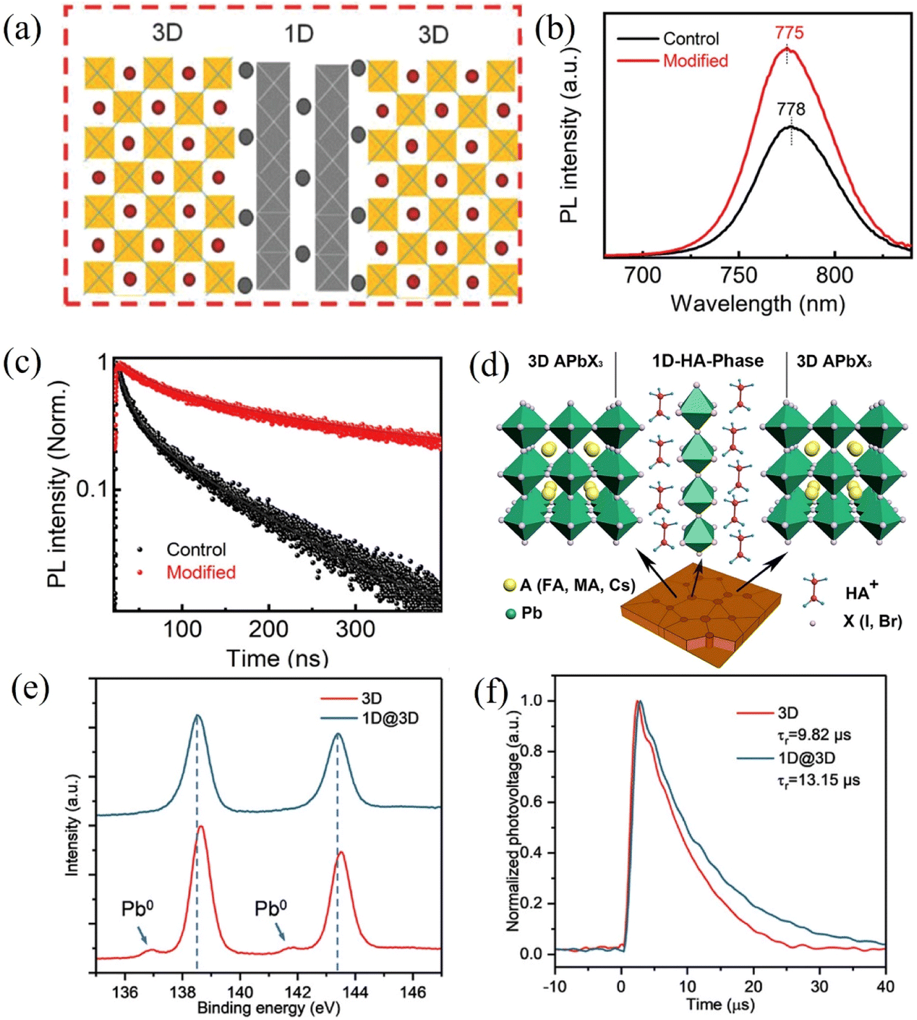 | ||
| Fig. 1 (a) Illustration of bulk 1D/3D perovskite heterojunctions.77 Copyright 2018, Wiley-VCH. (b and c) PL and TRPL spectra of control and DEAECCl-doped 1D/3D perovskite films.78 Copyright 2021, Wiley-VCH. (d) Illustration of the distribution of 1D perovskite in bulk 1D/3D perovskite heterojunctions.79 Copyright 2021, Elsevier. (e and f) Pb 4f XPS pattern and TPV spectra of both 3D and 1D/3D perovskite films.56 Copyright 2021, Wiley-VCH. | ||
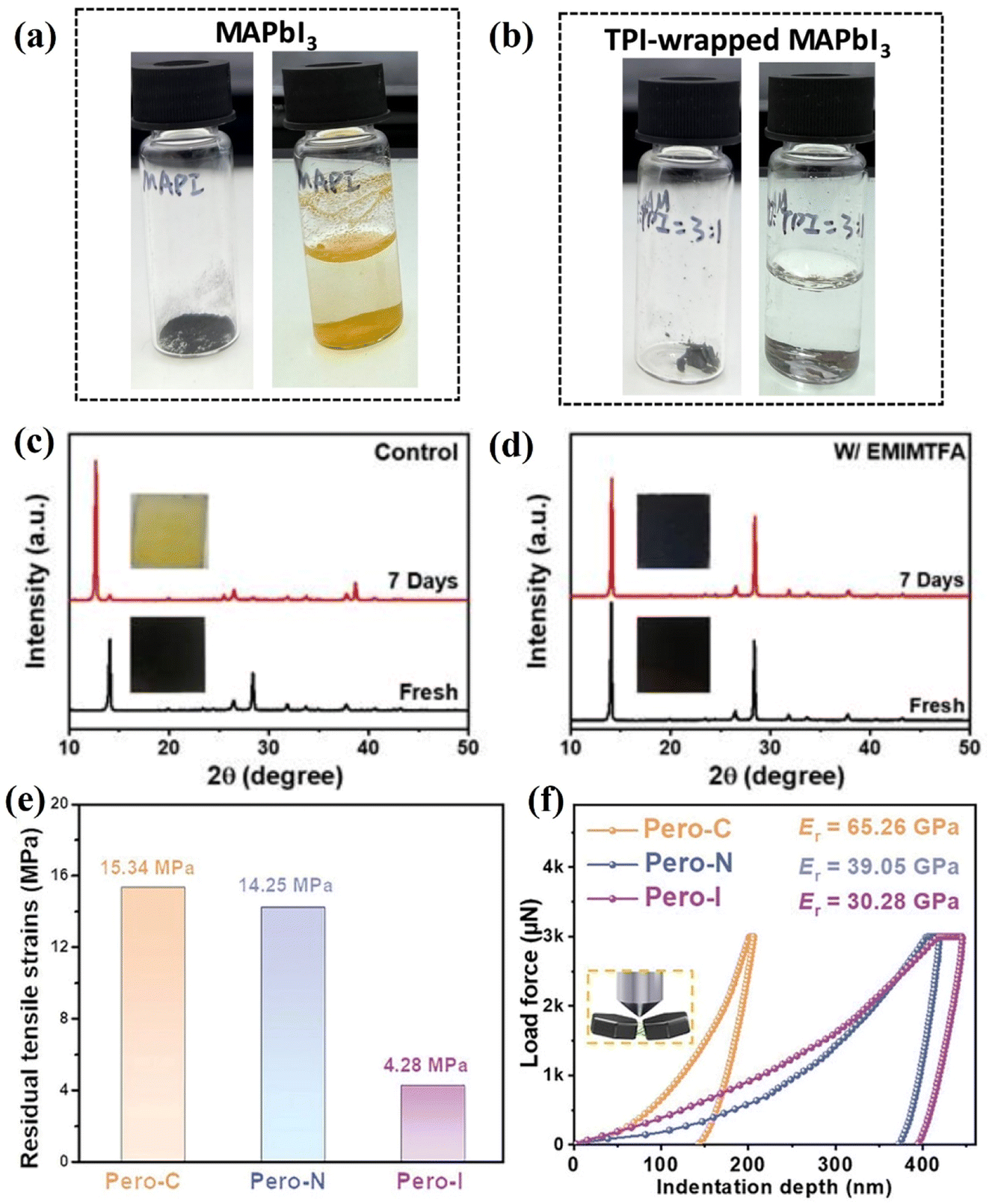
In addition to pursuing the high performance of PSCs, stability is also an indispensable part of PSCs. In order to ameliorate the situation, Jiao and co-authors introduced tributyl(methyl)phosphonium iodide (TPI) into a 3D perovskite precursor solution to convert perovskite GBs to 1D perovskite.80 As exhibited in Fig. 2a and b, the TPPbI3 powder had no clear color change after 12 h water soaking, while the MAPbI3 changed to yellow just within 10 s, which demonstrated that the 1D TPPbI3 perovskite had strong water resistance, which could protect the 3D perovskite from the moisture invade. Further, the TPI-treated 3D perovskite films also kept their original structure and no PbI2 appeared under 100 mW cm−2 light soaking in ambient air for 120 min (Fig. 2b). All of the above results showed that the 1D TPPbI3 perovskite could stabilize 3D perovskites in either moisture or light. In addition, the 3D perovskite film with TPI displayed a higher PL intensity and longer carrier recombination time than the control, demonstrating that the defects in GBs were effectively passivated. As a result, they realized a champion PCE of 22.9% higher than the control of 22.0%. And the device with TPI exhibited better stability and only a 7.8% reduction after 1900 h under 1 sun illumination at 55 °C, while the PCE of the control device decreased by 20.3% after 1877 h. Wei and co-authors employed the ionic liquid (IL) 1-ethyl-3-methylimidazolium trifluoroacetate (EMIMTFA) in perovskites to passivate defects and improve the stability of PSCs.81 After the incorporation of EMIMTFA, they found that the crystal structure had a stronger orientational preference in the vertical direction to the substrate than the control though grazing incidence wide-angle X-ray scattering (GIWAXS) measurement and there is a new diffraction ring at qz = 7.3 nm−1 corresponding to the 1D perovskite EMIMPbI3. The stronger PL intensity and elongated charge carrier lifetime imply the reduced defects density in 1D/3D perovskite heterojunction than the control. Further, the space-charge-limited current (SCLC) also showed that the trap density value decreased to 2.91 × 1015 cm−3 from 5.32 × 1015 cm−3. Thus, the defects in the perovskite film with EMIMTFA were passivated effectively. More importantly, the EMIMTFA-modified 3D perovskite film kept its initial properties either in the air at room temperature or 70 °C annealing for 7 days. As a result, the EMIMTFA-modified device obtained a champion PCE of 22.14% higher than the 18.93% for the control device. Even with continuous illumination for 550 h, 88% of its original PCE remained, while the control device only maintained about 40%. Chen and co-authors developed a cross-linkable monomer TA-NI for self-healing PSCs. The dynamic disulfide bonds, hydrogen bonds, and ammonium groups enable the TA-NI to have excellent mechanical properties. The low glass transition temperature further confirms the stretchability. When entering the elastic region, the TA-NI elastomer could fully recover. With the addition of TA-NI, the GIWAXS exhibited a new characteristic peak at q = 0.54 Å, and the PbI2 peak decreased significantly, which could be attributed to the 1D TAPbI3 perovskite. Based on the formation of 1D TAPbI3 perovskite, the residual tensile strains of the 3D perovskite film reduce from 15.34 MPa to 4.28 MPa and Young's modulus decreased from 65.26 GPa to 30.28 GPa. Thus, the 1D TAPbI3 perovskite could release the residual tensile strain through strain compensation. As a result, they achieve a champion PCE of 23.87% and 21.05% for rigid and flexible PSCs. Moreover, the flexible PSCs with a 1D/3D heterostructure maintained 94% of their initial PCE after bending 4000 times at a 5 mm radius, and with 1 h storage at room temperature, the PCE recovered to 97%.
 | ||
| Fig. 2 (a) Picture of 3D perovskite powder before and after soaking in water for 10 s. (b) Picture of 1D/3D perovskite powder before and after soaking in water for 12 h.80 Copyright 2022, Science. (c) XRD pattern of the 3D perovskite film before and after exposure to air at room temperature. (d) XRD pattern of the 1D/3D perovskite film before and after exposure to air at 70 °C.81 Copyright 2022, Wiley-VCH. (e) Residual tensile strains of the 3D and 1D/3D perovskite film. (f) Young's modulus of the 3D and 1D/3D perovskite film.82 Copyright 2023, Wiley-VCH. | ||
3.2 Interfacial 1D/3D perovskite heterojunctions
In addition to bulk 1D/3D perovskite heterojunctions, interfacial 1D/3D perovskite heterojunctions also play an important role in PSCs including passivating surface defects, modulating the energy level alignment and suppressing ion migration, leading to high performance and stability.33,35,91,96In 2016, Bi and co-authors employed the fluorinated cation CF3CH2NH3+ (FEA+) to tune the morphology of the perovskite layer.83 With the addition of FEAI, the perovskite film exhibited better morphology with low surface roughness, enhanced coverage, and more regular crystallites compared to the control film. The energy-dispersive X-ray spectrometry (EDS) showed that the fluorine element mainly existed on the surface of the crystal. Based on this distribution and the hydrophobicity of the fluorine alkyl group, the perovskite film with FEAI exhibited a large water contact than control, which implies that the perovskite film with FEAI had better moisture resistance. As a result, the FEAI-modified device achieved a champion PCE of 18.0%, and maintained 92% of its initial value after storage for 120 days in ambient air, while the PCE of control was 15.4% and declined 21% under the same storage conditions. Kaneko and co-author employed 4-tert-butylpyridinium iodide (TBPI) as the capping layer onto the perovskite film.84 After being spin-coated with TBPI, the gradient-structured 1D TBPPbI3 perovskite layer stacked parallel to the 3D perovskite, the XPS showed that the peak of Pb2+ shifted to lower binding energy, and the PL spectra exhibited enhanced intensity, and TRPL results displayed a longer carrier lifetime, demonstrating that the surface defects passivated and reduced nonradiative recombination. In addition, as a result, they achieved a maximum PCE of 19.3% higher than the control of 18.3%. Ge and co-authors added trimethylsulfonium iodide (Me3SI) into perovskite film and formed a 1D Me3SPbI3 nanoarray structure.85 After modification with Me3SI, the XPS pattern of the 1D/3D perovskite film showed that the binding energy of Pb2+ was lower, and the characteristic peak of Pb0 was diminished. Further, the PL intensity of the 1D/3D perovskite film was more uniform and higher than the control, and the TRPL showed a longer carrier lifetime, implying that the 1D perovskite passivated the surface defects, reduce the nonradiative recombination, and facilitate charge extraction and transport. As a result, they realized a maximum PCE of 22.07%. In addition, the 1D perovskite displayed better aprotic properties due to the enhanced water contact angle, and the device kept 97% of its original PCE after storage at ambient with 50% relative humidity (RH) for 1000 h. Wang and co-authors introduced 4-chlorobenzamidine hydrochloride (CBAH) to passivate the surface defects.86 Upon CBAH treatment, the binding energy of Pb2+ shifted to a higher area, confirming that CBAH reacted with PbI2, arching on the surface of the perovskite film and forming a 1D nanorod structure (Fig. 3a) and thus the surface defects passivated. Further, the higher PL intensity and elongated carrier lifetime revealed that the nonradiative recombination was suppressed, which agrees with the XPS result. As a result, the CBAH-treated device realized a champion PCE of 21.95%. The Lewis base or acid could be coordinated with Pb2+, which enabled it a good defect passivator in the PSCs. Chen and co-authors introduced 1,3-bis(aminomethyl)benzene dihydroiodide (m-PBAI2) to form 1D (m-PBA)Pb2I6 perovskite as the capping layer on 3D perovskite.87 With the modification of 1D perovskite, the ultraviolet photoemission spectroscopy (UPS) showed a valence band maximum (VBM) of −6.00 eV for the 1D/3D heterojunction, while the that of the control is −5.92 eV, implying that the capping layer could cause effective charge carrier quenching and Shockley–Read–Hall recombination. In addition, the XPS showed the Pb2+ characteristic peak at lower binding energy, thus the Pb-related defects are passivated by the introduced m-PBAI2. And the enhanced PL intensity and elongated carrier lifetime further confirmed that the defects were effectively passivated. As a result, they obtained a champion PCE of 23.84%. Moreover, with the capping layer, the water contact angle was increased from 52.91° to 76.03°, leading to better water resistance and thus the PSCs kept their 90% initial PCE after aging for 2000 h in ambient air.
 | ||
| Fig. 3 (a) Illustration of surface defect passivation of the 3D perovskite film.86 Copyright 2023, Wiley-VCH. (b) Energy dispersive spectra; Ag and I element analysis from the cross-section in (b) FTO/3D perovskite/Ag and (c) FTO/1D/3D perovskite/Ag device.88 Copyright 2019, American Chemical Society. (d and e) TOF-SIMS spectrum of 3D (d) and 1D/3D (e) perovskite films after 100 h 1 sun illumination with 85 °C heat.91 Copyright 2022, Wiley-VCH. | ||
Ion migration is a common problem, which induces lattice degradation during operation conditions and has been widely reported to be able to deteriorate device stability.25,97–102 Therefore, improving device stability not only enhances the water or/and oxygen resistance of perovskite film but suppresses ion migration is also important. Gao and co-authors utilized a short organic conjugated molecule thiazole ammonium iodide (TAI) to create a 1D TAPbI3 perovskite capping layer on 3D perovskite.88 With the TAI modification, the TAI reacted with PbI2 forming a smooth capping layer, which works as an encapsulating layer for the bulk 3D perovskite. Then, EDS was performed to determine the interdiffusion of silver (Ag) and iodine (I), as shown in Fig. 3b and c, there is almost no interdiffusion in the 1D/3D perovskite heterojunction structure, while in the control film, the Ag existed in 3D perovskite, and I migrated to the Ag layer, which confirmed that the 1D perovskite could effectively suppress ion migration. Besides, the PL and TRPL spectrum 1D/3D perovskite film displayed stronger intensity and longer carrier lifetime than the control, respectively, indicating that the 1D capping layer passivated the surface defects, and reduced nonradiative recombination. As a result, a champion PCE of 18.97% with negligible hysteresis had been obtained for the 1D/3D device and retained 92% of their initial PCE after aging for 1500 h in the dark with the temperature of 20 ± 5 °C and RH of 20 ± 10%. Zhan and co-authors introduced benzimidazole iodide (BnI) in the perovskite precursor solution.89 After incorporating BnI, the Bn+ coordinated with PbI2 through a Lewis acid–base reaction and formed 1D BnPbI3 perovskite, which was mainly distributed at the buried interface. With the 1D structure, the contact potential difference (ΔCPD) increased from 18 mV to 33 mV, resulting in lower surface potential than the bare 3D perovskite, facilitating charge extraction and transport and passivation of defects.102,103 In addition, when the perovskite film was illuminated from both sides, the 1D/3D perovskite film exhibited the same peak, while the 3D perovskite film showed a 4 nm shift, indicating that the 1D/3D perovskite film suppressed charge accumulation, enhancing the activation energy of ion migration. Further, the activation energy under an electro-strictive response was calculated to be 0.15 eV for the 1D/3D perovskite film, higher than that of the 3D perovskite film of 0.08 eV, and the ion conductivity decreased from 0.36 × 10⁻⁹ S cm−1 to 0.26 × 10⁻⁹ S cm−1, demonstrating that ion migration in the 1D/3D perovskite film was more difficult. As a result, the 1D/3D perovskite device achieved a champion PCE of 21.17% and retained 95.3% of its original PCE after 3072 h illumination under 1 sun in a nitrogen atmosphere. Chen incorporated 1,10-phenanthroline (Phen) to form 1D perovskite as a passivating layer.90 With Phen treatment, the 1D perovskite PbI2(Phen) formed on the surface of the 3D perovskite film through the reaction between Phen and excessive PbI2. The XRD showed that the Pb2+ peak of the 1D/3D perovskite film was lower than that of the control, indicating that the Pb-related defects were effectively passivated. More importantly, the XRD pattern of the perovskite/Ag sample showed the obvious peak of the δ-phase and AgI for the 3D perovskite film, while the signal in the 1D/3D perovskite film was quite low. Thus, the 1D structure not only passivated surface defects but alleviated the ion migration. As a result, the 1D/3D perovskite displayed a champion PCE of 23.3% and kept 80% of its original PCE after aging for 800 h in ambient air (50% RH). Chen and co-authors treated the surface of the perovskite film with benzimidazolium salts.91 After modification, the benzimidazolium group reacted with the [PbI6]4− chain and constructed 1D iprPbI3 perovskite, uniformly distributed on the surface of the 3D perovskite film. With the 1D perovskite, the 1D/3D film exhibited its original morphology after 50 h aging at 85 °C and 60% RH. In contrast, the 3D film exhibited an apparent yellow phase, confirming that the 1D/3D perovskite film had better water and thermal resistance. Further, when the device with and without the 1D perovskite was subjected to 100 h 1 sun illumination with 85 °C heat, the time-of-flight secondary ion mass spectrometry (TOF-SIMS) showed the signal of gold (Au) throughout the entire device in the bare 3D perovskite-based device, while the 1D/3D perovskite-based device showed almost no Au signal (Fig. 3d and e), demonstrating that the 1D perovskite film effectively suppressed ion migration. In addition, the 1D/3D perovskite film showed a stronger PL intensity with a smaller blueshift and longer τaverage compared to the 3D perovskite film, implying that the defects eliminated and suppressed nonradiative recombination. Further, the surface contact potential increased from −34.3 mV to 79.8 mV, and the VBM enhanced from −5.22 eV to −5.35 eV, facilitating the hole extraction and transfer. As a result, the 1D/3D perovskite-based device achieved a champion PCE of 19.61% for the 18 cm2 and 18.0% for 56 cm2 and the 1D/3D perovskite-based module retained 93% of its original PCE after aging for 1250 h under ambient conditions (25 °C, 40% RH).
4. 1D carrier transport layers
Carrier transport layers (CTL) play an important role in PSCs. The development of CTLs is critical to achieving stable and efficient PSCs. Traditional ETL or HTL films are usually based on mesoporous nanoparticles, which could not absorb light efficiently due to the short diffusion length (∼100 nm), and it is hard to fill the pore network with the perovskite. In contrast, the 1D CTL often has a single crystal or oriented structure, which could transport carriers effectively. Furthermore, the 1D CTL usually exhibits an open-pore structure that the perovskite could fully and uniformly fill into the pores, which could improve the contact and decrease the void, and finally ameliorate the performance of PSCs.104–109 Thus, the 1D CTL is a promising material for high-performance PSCs. Here, we discussed the recent progress of PSCs based on 1D CTLs as follows.Han and co-authors have grown 1D SnO2 nanowires (NWs) on the F:SnO2 (FTO) substrate through a vapor–liquid–solid reaction.106 Based on the adjustment of temperature, time and oxygen flow rate, they obtained the optimized SnO2 NWs with 300 nm long and 20 nm thickness. These SnO2 NWs are paralleled with axial direction with sparse stack, facilitating the perovskite pore-filling. After being integrated into the PSC device, the SnO2 NW-based device exhibited a higher electron diffusion coefficient than the traditional mp-ETL devices, leading to higher photon-to-current efficiency, confirming that the 1D SnO2 NWs had better electron-collection efficiency. As a result, they achieved a champion PCE of 14.2% with a higher fill factor (FF). Tao and co-authors employed 1D TiO2 NWs to ameliorate the interface.110 The 1D film showed a larger porosity and surface area, which was better for the pore-fill of perovskite, resulting in uniformly distributed perovskite crystals with a larger size than the nanoparticle ETL. Thus, the device with 1D TiO2 NWs obtained a champion PCE of 12.78%, while the nanoparticle-based device was 9.59%. Lee and co-authors 1D mesoporous silica (mSiO2) nanorods on the compact TiO2 layer through a modified Stöber method.111 The randomly stacked mSiO2 nanorods provided more voids for the penetration of perovskite, increasing the precursor infiltration and pore-filling. With the mSiO2 nanorods, the perovskite film showed stronger PL intensity and longer PL decay lifetime, indicating that the electron transport had been improved. In addition, electrochemical impedance spectroscopy (EIS) spectra showed a lower interfacial charge transfer resistance of the PSC device with mSiO2 nanorods compared to the device without mSiO2 nanorods. As a result, they obtained a champion PCE of 13.91% while that of the control was 12.36%. Wu and co-authors had grown 1D TiO2 on the FTO substrate via the solvothermal route as the ETL.37 The ETL exhibited an NW morphology with a diameter of 5–15 nm and an open structure. Besides, the 1D TiO2 NWs had a preferential orientation along the c-axis direction, which facilitated the perovskite pore-filling, inducing reduced charger carrier collection path length (Fig. 4a). Further, the 1D TiO2 NWs on the FTO substrate showed a higher optical transmittance and haze factor than the bare FTO, demonstrating that the 1D TiO2 NWs film ameliorates the light harvesting and trapping capability. Based on these properties, the PL of perovskite on the 1D TiO2 NWs quenched significantly compared to the perovskite film deposited on the bare FTO substrate, indicating that the fast charge extraction and transfer between the perovskite and the 1D TiO2 NW ETL. As a result, the PSC devices with 1D ETLs realized a champion PCE of 16.04%.
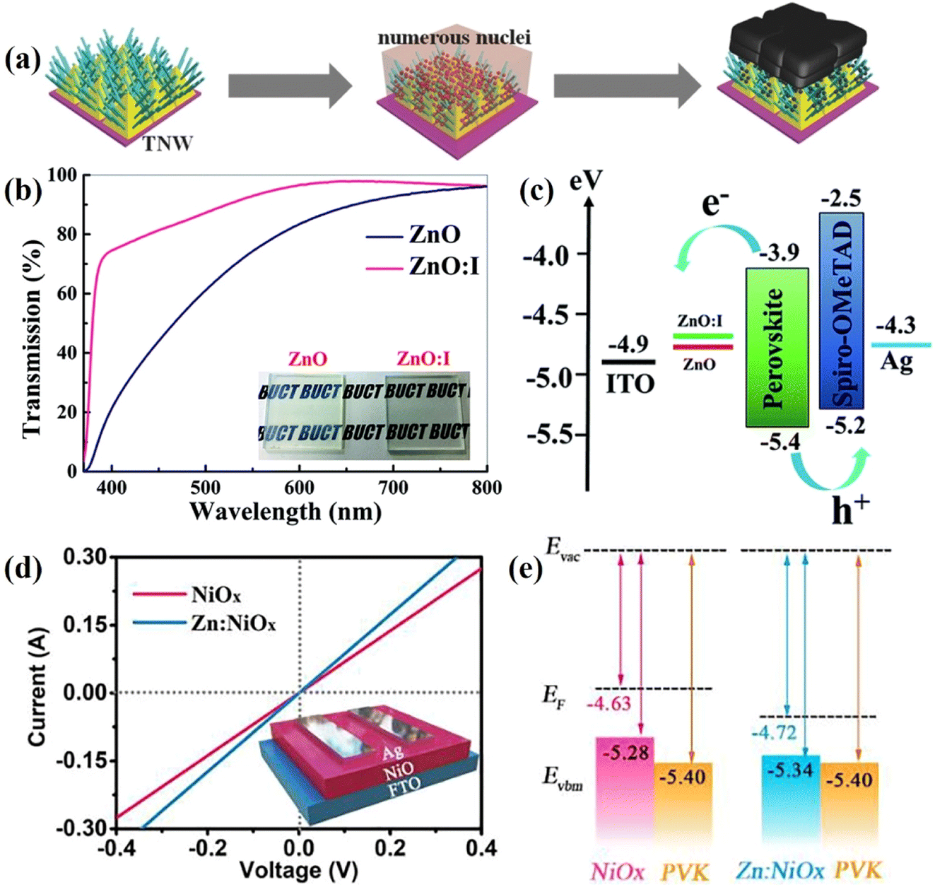 | ||
| Fig. 4 (a) Illustration of nuclei density and crystal growth of perovskite on TiO2 NWs.37 Copyright 2016, Wiley-VCH. (b) The transmittance of ZnO and ZnO:I film. (c) Energy level alignment of the PSCs with different ETLs.113 Copyright 2017, Royal Society of Chemistry. (d) I–V curve of the hole-only device with different HTLs. (e) Energy level diagram of two HTLs with perovskite.115 Copyright 2023, Elsevier. | ||
In addition to the better perovskite pore-filling, conductivity and energy level alignment are also important to the performance of PSCs. Batmunkh and co-authors incorporated single-walled nanotubes (SWNT) into the 1D TiO2 nanofiber (SWNT-TiO2 NFs) as the ETL to ameliorate the PCE of PSCs.112 With the doping of SWNTs, the sheet resistance (Rs) was decreased significantly, enhancing the conductivity and accelerating the charge transport. Moreover, the CBM of THE TiO2 ETL was calculated to be 0.58 eV, while the work function of the SWNT-TiO2 NFs ETL was 0.35 eV, higher than the CBM of the TiO2 ETL, leading to higher VOC. As a result, the SWNT-doped device realized a champion PCE of 14.03, while that of the control device was 8.16%. Zheng and co-authors utilized the iodine-doped ZnO (ZnO:I) nanorod as the ETL.113 With the incorporation of I, the ZnO:I ETL displayed an improved transmittance than the ZnO ETL, implying that the ZnO:I ETL ameliorated the light harvesting capability. Moreover, the work function of ZnO:I also decreased to 4.71 eV from 4.79 eV of ZnO, and the internal resistance of ZnO:I-based PSCs decreased to 33.5 Ω from 59.8 of ZnO-based PSCs, improving the electron extraction and transport. The PL and TRPL spectrum exhibited lower PL intensity and shorter PL lifetime, further confirming the efficient electron extraction between the ZnO:I ETL and perovskite interface. As a result, the ZnO:I-based PSCs achieved a champion PCE of 18.24%, higher than that of the ZnO-based PSCs of 10.79%. Hu and co-authors employed 1D cation-doped TiO2 nanorods with embedded fullerene (C60:M-TiO2, M = Fe, ferrum or Co, cobalt) as the ETL in inverted PSCs.114 With the treatment of metal cations, the conductivity slightly improved from 0.56 mS m−1 of pristine C60 to 0.66 mS m−1 of C60:Co-TiO2, leading to higher electron mobility. In addition, the doped metal cation alleviated the energy level mismatch. Before doping, the CBM difference between the perovskite and C60 was 170 meV, after incorporating the metal cation, the energy level mismatch decreased to 40 meV and 90 meV, and the ameliorated energy alignment led to efficient interfacial charge transfer. As a result, the device doped with Co cations achieved a champion PCE of 22.13%. Yin and co-authors Zn-doped NiOX (Zn:NiOX) to change the optoelectronic properties of NiOX.115 They utilize the template-assisted cation exchange strategy to convert the ZnO nanorod arrays into NiOX nanorod arrays. After Zn was doped into NiOX, the conductivity of Zn:NiOX was increased to 5.85 × 10⁻⁴ S cm−1, and the Fermi level and valence band maximum were reduced to 4.69 eV and −5.34 eV, which is more aligned with the perovskite (−5.40 eV). All of these facilitated the transportation of holes and reduced the recombination. The stronger PL quenching and shorter carrier lifetime of TRPL were also observed for the Zn:NiOX/perovskite sample, which is consistent with the above result. As a result, a champion PCE of 19.83% with an enhanced VOC of 1.14 V was achieved. Further, the stability is also improved and 82% of the initial PCE was maintained after storing for 600 h in ambient air.
5. Summary and outlook
This review is focused on the recent development of 1D material-based PSCs with high performance and stability. Although some achievements have been made in 1D material-based PSCs, there are still some issues that need to be addressed.Compared to 3D perovskites, systematic research on 1D perovskites is lacking. For example, the current synthesis method of 1D materials is still trial-and-error. With the existence of machine learning techniques,116–118 Lu and co-authors predicted numerous perovskite structures based on previous databases.119 Maybe these techniques could guide us to synthesize the perovskite structure we desired. Further, most of the 1D perovskites were obtained by additive engineering or interface modification. Although these methods are very simple, it is difficult to precisely control the size of 1D perovskites and their distribution in 3D perovskites. Thus, how to control the size and distribution needs in-depth research. In addition to the synthesis and distribution, the photophysical processes and optoelectronic properties of 1D materials also should be investigated deeply. Finally, it is highly expected to simultaneously construct 1D/3D bulk and interfacial heterojunctions in order to minimize bulk and interfacial nonradiative recombination losses.
Apart from 1D perovskites, developing 1D carrier transport layers is also very important for further enhancing photovoltaic performance by facilitating interfacial carrier extraction and transport and inhibiting interfacial nonradiative recombination. In spite of obtaining some advancements, the correlation between the structure and morphology of 1D carrier transport layers and device performance as well as interfacial carrier dynamics should be deeply uncovered. It is imperative and important to precisely control the orientation, size, morphology and optoelectronic properties of 1D carrier transport materials for maximizing their potential.
Last but not least, the stability of PSCs still has a long way to go before commercialization. Thus, the degradation mechanism based on different factors (oxygen, water, heat, etc.) should be investigated systematically. The stability enhancement mechanisms of 1D materials in PSCs should be clearly revealed in order to guide the design of more effective 1D materials to advance the development of perovskite photovoltaic technology.
Conflicts of interest
The authors declare no conflict of interest.Acknowledgements
This work was financially supported by the National Natural Science Foundation of China (62274018).References
- G. Xing, N. Mathews, S. Sun, S. S. Lim, Y. M. Lam, M. Grätzel, S. Mhaisalkar and T. C. Sum, Science, 2013, 342, 344–347 CrossRef CAS PubMed.
- A. R. b. Mohd Yusoff, M. Vasilopoulou, D. G. Georgiadou, L. C. Palilis, A. Abate and M. K. Nazeeruddin, Energy Environ. Sci., 2021, 14, 2906–2953 RSC.
- G. Tang and F. Yan, Nano Today, 2021, 39, 101155 CrossRef CAS.
- B. Chen, P. N. Rudd, S. Yang, Y. Yuan and J. Huang, Chem. Soc. Rev., 2019, 48, 3842–3867 RSC.
- J.-W. Lee, D.-J. Seol, A.-N. Cho and N.-G. Park, Adv. Mater., 2014, 26, 4991–4998 CrossRef CAS.
- C. Wehrenfennig, G. E. Eperon, M. B. Johnston, H. J. Snaith and L. M. Herz, Adv. Mater., 2014, 26, 1584–1589 CrossRef CAS PubMed.
- M. A. Green, Y. Jiang, A. M. Soufiani and A. Ho-Baillie, J. Phys. Chem. Lett., 2015, 6, 4774–4785 CrossRef CAS PubMed.
- A. Kojima, K. Teshima, Y. Shirai and T. Miyasaka, J. Am. Chem. Soc., 2009, 131, 6050–6051 CrossRef CAS PubMed.
- J. Park, J. Kim, H.-S. Yun, M. J. Paik, E. Noh, H. J. Mun, M. G. Kim, T. J. Shin and S. I. Seok, Nature, 2023, 616, 724–730 CrossRef CAS PubMed.
- B. Liu, R. Li, Q. Zhuang, X. Yu, S. Gong, D. He, Q. Zhou, H. Yang, X. Chen, S. Lu, Z.-X. Xu, Z. Zang and J. Chen, J. Energy Chem., 2023, 76, 277–287 CrossRef CAS.
- Q. Zhou, D. He, Q. Zhuang, B. Liu, R. Li, H. Li, Z. Zhang, H. Yang, P. Zhao, Y. He, Z. Zang and J. Chen, Adv. Funct. Mater., 2022, 32, 2205507 CrossRef CAS.
- D.-J. Xue, Y. Hou, S.-C. Liu, M. Wei, B. Chen, Z. Huang, Z. Li, B. Sun, A. H. Proppe, Y. Dong, M. I. Saidaminov, S. O. Kelley, J.-S. Hu and E. H. Sargent, Nat. Commun., 2020, 11, 1514 CrossRef CAS.
- W. Zhou, S. Chen, Y. Zhao, Q. Li, Y. Zhao, R. Fu, D. Yu, P. Gao and Q. Zhao, Adv. Funct. Mater., 2019, 29, 1809180 CrossRef.
- J. Jeong, M. Kim, J. Seo, H. Lu, P. Ahlawat, A. Mishra, Y. Yang, M. A. Hope, F. T. Eickemeyer, M. Kim, Y. J. Yoon, I. W. Choi, B. P. Darwich, S. J. Choi, Y. Jo, J. H. Lee, B. Walker, S. M. Zakeeruddin, L. Emsley, U. Rothlisberger, A. Hagfeldt, D. S. Kim, M. Grätzel and J. Y. Kim, Nature, 2021, 592, 381–385 CrossRef CAS PubMed.
- D. Liu, D. Luo, A. N. Iqbal, K. W. P. Orr, T. A. S. Doherty, Z.-H. Lu, S. D. Stranks and W. Zhang, Nat. Mater., 2021, 20, 1337–1346 CrossRef CAS PubMed.
- B. Liu, H. Bi, D. He, L. Bai, W. Wang, H. Yuan, Q. Song, P. Su, Z. Zang, T. Zhou and J. Chen, ACS Energy Lett., 2021, 6, 2526–2538 CrossRef CAS.
- T.-H. Han, S. Tan, J. Xue, L. Meng, J.-W. Lee and Y. Yang, Adv. Mater., 2019, 31, 1803515 CrossRef CAS PubMed.
- H. Bi, B. Liu, D. He, L. Bai, W. Wang, Z. Zang and J. Chen, Chem. Eng. J., 2021, 418, 129375 CrossRef CAS.
- J. Chen, Y. Xiong, Y. Rong, A. Mei, Y. Sheng, P. Jiang, Y. Hu, X. Li and H. Han, Nano Energy, 2016, 27, 130–137 CrossRef CAS.
- W. A. Dunlap-Shohl, Y. Zhou, N. P. Padture and D. B. Mitzi, Chem. Rev., 2019, 119, 3193–3295 CrossRef CAS PubMed.
- T. Li, Y. Pan, Z. Wang, Y. Xia, Y. Chen and W. Huang, J. Mater. Chem. A, 2017, 5, 12602–12652 RSC.
- F. Zhang and K. Zhu, Adv. Energy Mater., 2020, 10, 1902579 CrossRef CAS.
- J. Chen, S.-G. Kim, X. Ren, H. S. Jung and N.-G. Park, J. Mater. Chem. A, 2019, 7, 4977–4987 RSC.
- M. Li, H. Li, Q. Zhuang, D. He, B. Liu, C. Chen, B. Zhang, T. Pauporté, Z. Zang and J. Chen, Angew. Chem., Int. Ed., 2022, 61, e202206914 CrossRef CAS.
- J. Chen and N.-G. Park, Adv. Mater., 2019, 31, 1803019 CrossRef CAS PubMed.
- K. Wang, W. S. Subhani, Y. Wang, X. Zuo, H. Wang, L. Duan and S. Liu, Adv. Mater., 2019, 31, 1902037 CrossRef CAS.
- D. Thrithamarassery Gangadharan and D. Ma, Energy Environ. Sci., 2019, 12, 2860–2889 RSC.
- J. Chen, D. Lee and N.-G. Park, ACS Appl. Mater. Interfaces, 2017, 9, 36338–36349 CrossRef CAS PubMed.
- Y. Zhao, H. Xiang, R. Ran, W. Zhou, W. Wang and Z. Shao, J. Energy Chem., 2023, 83, 189–208 CrossRef CAS.
- Y. Gao, X. Dong and Y. Liu, Nano-Micro Lett., 2023, 15, 169 CrossRef CAS PubMed.
- X. Zhao, T. Liu and Y.-L. Loo, Adv. Mater., 2022, 34, 2105849 CrossRef CAS PubMed.
- Q. Zhou, B. Liu, X. Shai, Y. Li, P. He, H. Yu, C. Chen, Z.-X. Xu, D. Wei and J. Chen, Chem. Commun., 2023, 59, 4128–4141 RSC.
- J. Chen, J.-Y. Seo and N.-G. Park, Adv. Energy Mater., 2018, 8, 1702714 CrossRef.
- H. Li, C. Zhang, C. Gong, D. Zhang, H. Zhang, Q. Zhuang, X. Yu, S. Gong, X. Chen, J. Yang, X. Li, R. Li, J. Li, J. Zhou, H. Yang, Q. Lin, J. Chu, M. Grätzel, J. Chen and Z. Zang, Nat. Energy, 2023 DOI:10.1038/s41560-023-01295-8.
- S. Sidhik, Y. Wang, M. De Siena, R. Asadpour, A. J. Torma, T. Terlier, K. Ho, W. Li, A. B. Puthirath, X. Shuai, A. Agrawal, B. Traore, M. Jones, R. Giridharagopal, P. M. Ajayan, J. Strzalka, D. S. Ginger, C. Katan, M. A. Alam, J. Even, M. G. Kanatzidis and A. D. Mohite, Science, 2022, 377, 1425–1430 CrossRef CAS PubMed.
- R. Azmi, E. Ugur, A. Seitkhan, F. Aljamaan, A. S. Subbiah, J. Liu, G. T. Harrison, M. I. Nugraha, M. K. Eswaran, M. Babics, Y. Chen, F. Xu, T. G. Allen, A. u. Rehman, C.-L. Wang, T. D. Anthopoulos, U. Schwingenschlögl, M. De Bastiani, E. Aydin and S. De Wolf, Science, 2022, 376, 73–77 CrossRef CAS PubMed.
- W.-Q. Wu, F. Huang, D. Chen, Y.-B. Cheng and R. A. Caruso, Adv. Energy Mater., 2016, 6, 1502027 CrossRef.
- J. Feng, X. Zhu, Z. Yang, X. Zhang, J. Niu, Z. Wang, S. Zuo, S. Priya, S. Liu and D. Yang, Adv. Mater., 2018, 30, 1801418 CrossRef PubMed.
- D. Yao, M. T. Hoang and H. Wang, Small Methods, 2021, 5, 2001147 CrossRef CAS PubMed.
- L. Zhang, K. Wang, Y. Lin and B. Zou, J. Phys. Chem. Lett., 2020, 11, 4693–4701 CrossRef CAS PubMed.
- C. Zhou, H. Lin, Q. He, L. Xu, M. Worku, M. Chaaban, S. Lee, X. Shi, M.-H. Du and B. Ma, Mater. Sci. Eng. R Rep., 2019, 137, 38–65 CrossRef.
- P. Zhu and J. Zhu, InfoMat, 2020, 2, 341–378 CrossRef CAS.
- M. I. Saidaminov, O. F. Mohammed and O. M. Bakr, ACS Energy Lett., 2017, 2, 889–896 CrossRef CAS.
- C. Zhang, J. Chen, S. Wang, L. Kong, S. W. Lewis, X. Yang, A. L. Rogach and G. Jia, Adv. Mater., 2020, 32, 2002736 CrossRef CAS PubMed.
- G. E. Eperon, S. D. Stranks, C. Menelaou, M. B. Johnston, L. M. Herz and H. J. Snaith, Energy Environ. Sci., 2014, 7, 982–988 RSC.
- M. Kulbak, D. Cahen and G. Hodes, J. Phys. Chem. Lett., 2015, 6, 2452–2456 CrossRef CAS.
- N. J. Jeon, J. H. Noh, W. S. Yang, Y. C. Kim, S. Ryu, J. Seo and S. I. Seok, Nature, 2015, 517, 476–480 CrossRef CAS PubMed.
- D. B. Mitzi, S. Wang, C. A. Feild, C. A. Chess and A. M. Guloy, Sci. Adv., 1995, 267, 1473–1476 CAS.
- V. D'Innocenzo, G. Grancini, M. J. P. Alcocer, A. R. S. Kandada, S. D. Stranks, M. M. Lee, G. Lanzani, H. J. Snaith and A. Petrozza, Nat. Commun., 2014, 5, 3586 CrossRef PubMed.
- J. S. Manser and P. V. Kamat, Nat. Photonics, 2014, 8, 737–743 CrossRef CAS.
- A. Miyata, A. Mitioglu, P. Plochocka, O. Portugall, J. T.-W. Wang, S. D. Stranks, H. J. Snaith and R. J. Nicholas, Nat. Phys., 2015, 11, 582–587 Search PubMed.
- K. Tanaka, F. Sano, T. Takahashi, T. Kondo, R. Ito and K. Ema, Solid State Commun., 2002, 122, 249–252 CrossRef CAS.
- Y. Gao, Z. Wei, S.-N. Hsu, B. W. Boudouris and L. Dou, Mater. Chem. Front., 2020, 4, 3400–3418 RSC.
- Q. Chang, F. Wang, W. Xu, A. Wang, Y. Liu, J. Wang, Y. Yun, S. Gao, K. Xiao, L. Zhang, L. Wang, J. Wang, W. Huang and T. Qin, Angew. Chem., Int. Ed., 2021, 60, 25567–25574 CrossRef CAS PubMed.
- X. Li, G. Wu, M. Wang, B. Yu, J. Zhou, B. Wang, X. Zhang, H. Xia, S. Yue, K. Wang, C. Zhang, J. Zhang, H. Zhou and Y. Zhang, Adv. Energy Mater., 2020, 10, 2001832 CrossRef CAS.
- J. Wu, Y. Li, Y. Zhang, Y. Li, Y. Huang, Z. Jiang, Q. Ai, Y. Liu, L. Zhang, Y. Peng, X. Wang, B. Xu and C. Cheng, Small, 2022, 18, 2200130 CrossRef CAS PubMed.
- H. Tsai, W. Nie, J.-C. Blancon, C. C. Stoumpos, R. Asadpour, B. Harutyunyan, A. J. Neukirch, R. Verduzco, J. J. Crochet, S. Tretiak, L. Pedesseau, J. Even, M. A. Alam, G. Gupta, J. Lou, P. M. Ajayan, M. J. Bedzyk, M. G. Kanatzidis and A. D. Mohite, Nature, 2016, 536, 312–316 CrossRef CAS PubMed.
- N. Li, Z. Zhu, C.-C. Chueh, H. Liu, B. Peng, A. Petrone, X. Li, L. Wang and A. K.-Y. Jen, Adv. Energy Mater., 2017, 7, 1601307 CrossRef.
- P. Qin, M. Paulose, M. I. Dar, T. Moehl, N. Arora, P. Gao, O. K. Varghese, M. Grätzel and M. K. Nazeeruddin, Small, 2015, 11, 5533–5539 CrossRef CAS PubMed.
- P. E. de Jongh and D. Vanmaekelbergh, Phys. Rev. Lett., 1996, 77, 3427–3430 CrossRef CAS PubMed.
- D. Gao, R. Li, X. Chen, C. Chen, C. Wang, B. Zhang, M. Li, X. Shang, X. Yu, S. Gong, T. Pauporté, H. Yang, L. Ding, J. Tang and J. Chen, Adv. Mater., 2023, 2301028, DOI:10.1002/adma.202301028.
- J. Chen, S. Zhou, S. Jin, H. Li and T. Zhai, J. Mater. Chem. C, 2016, 4, 11–27 RSC.
- Y. Zhang, Y. Wang, Z.-Q. Xu, J. Liu, J. Song, Y. Xue, Z. Wang, J. Zheng, L. Jiang, C. Zheng, F. Huang, B. Sun, Y.-B. Cheng and Q. Bao, ACS Nano, 2016, 10, 7031–7038 CrossRef CAS PubMed.
- J. Chen, Y. Fu, L. Samad, L. Dang, Y. Zhao, S. Shen, L. Guo and S. Jin, Nano Lett., 2017, 17, 460–466 CrossRef CAS PubMed.
- S. T. Ha, X. F. Liu, Q. Zhang, D. Giovanni, T. C. Sum and Q. H. Xiong, Adv. Opt. Mater., 2014, 2, 838–844 CrossRef CAS.
- K. Park, J. W. Lee, J. D. Kim, N. S. Han, D. M. Jang, S. Jeong, J. Park and J. K. Song, J. Phys. Chem. Lett., 2016, 7, 3703–3710 CrossRef CAS PubMed.
- E. Horváth, M. Spina, Z. Szekrényes, K. Kamarás, R. Gaal, D. Gachet and L. Forró, Nano Lett., 2014, 14(12), 6761–6766 CrossRef PubMed.
- Y. P. Fu, H. M. Zhu, A. W. Schrader, D. Liang, Q. Ding, P. Joshi, L. Hwang, X. Y. Zhu and S. Jin, Nano Lett., 2016, 16, 1000–1008 CrossRef CAS PubMed.
- S. W. Eaton, M. L. Lai, N. A. Gibson, A. B. Wong, L. T. Dou, J. Ma, L. W. Wang, S. R. Leone and P. D. Yang, Proc. Natl. Acad. Sci. U. S. A, 2016, 113, 1993–1998 CrossRef CAS PubMed.
- Y. Tong, B. J. Bohn, E. Bladt, K. Wang, P. Muller-Buschbaum, S. Bals, A. S. Urban, L. Polavarapu and J. Feldmann, Angew. Chem., Int. Ed., 2017, 56, 13887–13892 CrossRef CAS PubMed.
- F. Zhu, L. Men, Y. J. Guo, Q. C. Zhu, U. Bhattacharjee, P. M. Goodwin, J. W. Petrich, E. A. Smith and J. Vela, ACS Nano, 2015, 9, 2948–2959 CrossRef CAS PubMed.
- D. D. Zhang, S. W. Eaton, Y. Yu, L. T. Dou and P. D. Yang, J. Am. Chem. Soc., 2015, 137, 9230–9233 CrossRef CAS PubMed.
- D. Zhang, Y. Yu, Y. Bekenstein, A. B. Wong, A. P. Alivisatos and P. Yang, J. Am. Chem. Soc., 2016, 138, 13155–13158 CrossRef CAS PubMed.
- D. D. Zhang, Y. M. Yang, Y. Bekenstein, Y. Yu, N. A. Gibson, A. B. Wong, S. W. Eaton, N. Kornienko, Q. Kong, M. L. Lai, A. P. Alivisatos, S. R. Leone and P. D. Yang, J. Am. Chem. Soc., 2016, 138, 7236–7239 CrossRef CAS PubMed.
- M. J. Ashley, M. N. O'Brien, K. R. Hedderick, J. A. Mason, M. B. Ross and C. A. Mirkin, J. Am. Chem. Soc., 2016, 138, 10096–10099 CrossRef CAS PubMed.
- S. Z. Oener, P. Khoram, S. Brittman, S. A. Mann, Q. Zhang, Z. Fan, S. W. Boettcher and E. C. Garnett, Nano Lett., 2017, 17, 6557–6563 CrossRef CAS PubMed.
- J. Fan, Y. Ma, C. Zhang, C. Liu, W. Li, R. E. I. Schropp and Y. Mai, Adv. Energy Mater., 2018, 8, 1703421 CrossRef.
- T. Kong, H. Xie, Y. Zhang, J. Song, Y. Li, E. L. Lim, A. Hagfeldt and D. Bi, Adv. Energy Mater., 2021, 11, 2101018 CrossRef CAS.
- S. Yu, H. Liu, S. Wang, H. Zhu, X. Dong and X. Li, Chem. Eng. J., 2021, 403, 125724 CrossRef CAS.
- H. Jiao, Z. Ni, Z. Shi, C. Fei, Y. Liu, X. Dai and J. Huang, Sci. Adv., 2022, 8, eabq4524 CrossRef CAS PubMed.
- N. Wei, Y. Chen, X. Wang, Y. Miao, Z. Qin, X. Liu, H. Wei and Y. Zhao, Adv. Funct. Mater., 2022, 32, 2108944 CrossRef CAS.
- Z. Chen, Q. Cheng, H. Chen, Y. Wu, J. Ding, X. Wu, H. Yang, H. Liu, W. Chen, X. Tang, X. Lu, Y. Li and Y. Li, Adv. Mater., 2023, 35, 2300513 CrossRef CAS PubMed.
- D. Bi, P. Gao, R. Scopelliti, E. Oveisi, J. Luo, M. Grätzel, A. Hagfeldt and M. K. Nazeeruddin, Adv. Mater., 2016, 28, 2910–2915 CrossRef CAS PubMed.
- R. Kaneko, H. Kanda, N. Shibayama, K. Sugawa, J. Otsuki, A. Islam and M. K. Nazeeruddin, Sol. RRL, 2021, 5, 2000791 CrossRef CAS.
- C. Ge, J.-F. Lu, M. Singh, A. Ng, W. Yu, H. Lin, S. Satapathi and H. Hu, Sol. RRL, 2022, 6, 2100879 CrossRef CAS.
- J. Wang, L. Liu, S. Chen, L. Qi, M. Zhao, C. Zhao, J. Tang, X. Cai, F. Lu and T. Jiu, Small, 2022, 18, 2104100 CrossRef CAS PubMed.
- J. Chen, Y. Yang, H. Dong, J. Li, X. Zhu, J. Xu, F. Pan, F. Yuan, J. Dai, B. Jiao, X. Hou, A. K.-Y. Jen and Z. Wu, Sci. Adv., 2022, 8, eabk2722 CrossRef CAS PubMed.
- L. Gao, I. Spanopoulos, W. Ke, S. Huang, I. Hadar, L. Chen, X. Li, G. Yang and M. G. Kanatzidis, ACS Energy Lett., 2019, 4, 1763–1769 CrossRef CAS.
- Y. Zhan, F. Yang, W. Chen, H. Chen, Y. Shen, Y. Li and Y. Li, Adv. Mater., 2021, 33, 2105170 CrossRef CAS PubMed.
- Q. Chen, K. Deng, Y. Shen and L. Li, InfoMat, 2022, 4, e12303 CAS.
- R. Azmi, E. Ugur, A. Seitkhan, F. Aljamaan, A. S. Subbiah, J. Liu, G. T. Harrison, M. I. Nugraha, M. K. Eswaran, M. Babics, Y. Chen, F. Xu, T. G. Allen, A. u. Rehman, C.-L. Wang, T. D. Anthopoulos, U. Schwingenschlögl, M. De Bastiani, E. Aydin and S. De Wolf, Science, 2022, 376, 73–77 CrossRef CAS PubMed.
- Y. Cai, J. Cui, M. Chen, M. Zhang, Y. Han, F. Qian, H. Zhao, S. Yang, Z. Yang, H. Bian, T. Wang, K. Guo, M. Cai, S. Dai, Z. Liu and S. Liu, Adv. Funct. Mater., 2021, 31, 2005776 CrossRef CAS.
- X. Yang, D. Luo, Y. Xiang, L. Zhao, M. Anaya, Y. Shen, J. Wu, W. Yang, Y.-H. Chiang, Y. Tu, R. Su, Q. Hu, H. Yu, G. Shao, W. Huang, T. P. Russell, Q. Gong, S. D. Stranks, W. Zhang and R. Zhu, Adv. Mater., 2021, 33, 2006435 CrossRef CAS PubMed.
- H. Zhang, Z. Shi, L. Hu, Y.-Y. Tang, Z. Qin, W.-Q. Liao, Z. S. Wang, J. Qin, X. Li, H. Wang, M. Gusain, F. Liu, Y. Pan, M. Xu, J. Wang, R. Liu, C. Zhang, R.-G. Xiong, W. E. I. Sha and Y. Zhan, Adv. Funct. Mater., 2021, 31, 2100205 CrossRef CAS.
- C. Ma, D. Shen, B. Huang, X. Li, W.-C. Chen, M.-F. Lo, P. Wang, M. Hon-Wah Lam, Y. Lu, B. Ma and C.-S. Lee, J. Mater. Chem. A, 2019, 7, 8811–8817 RSC.
- A. F. Xu, N. Liu, F. Xie, T. Song, Y. Ma, P. Zhang, Y. Bai, Y. Li, Q. Chen and G. Xu, Nano Lett., 2020, 20, 3864–3871 CrossRef CAS PubMed.
- J. Chen and N.-G. Park, ACS Energy Lett., 2020, 5, 2742–2786 CrossRef CAS.
- Y. Wang, T. Wu, J. Barbaud, W. Kong, D. Cui, H. Chen, X. Yang and L. Han, Science, 2019, 365, 687–691 CrossRef CAS PubMed.
- J. Zhao, Y. Deng, H. Wei, X. Zheng, Z. Yu, Y. Shao, J. E. Shield and J. Huang, Sci. Adv., 2017, 3, eaao5616 CrossRef PubMed.
- B. Chen, T. Li, Q. Dong, E. Mosconi, J. Song, Z. Chen, Y. Deng, Y. Liu, S. Ducharme, A. Gruverman, F. D. Angelis and J. Huang, Nat. Mater., 2018, 17, 1020–1026 CrossRef CAS PubMed.
- Q. Chen, H. Zhou, T.-B. Song, S. Luo, Z. Hong, H.-S. Duan, L. Dou, Y. Liu and Y. Yang, Nano Lett., 2014, 14, 4158–4163 CrossRef CAS PubMed.
- J. S. Yun, A. Ho-Baillie, S. Huang, S. H. Woo, Y. Heo, J. Seidel, F. Huang, Y.-B. Cheng and M. A. Green, J. Phys. Chem. Lett., 2015, 6, 875–880 CrossRef CAS PubMed.
- H. Chen, Y. Zhan, G. Xu, W. Chen, S. Wang, M. Zhang, Y. Li and Y. Li, Adv. Funct. Mater., 2020, 30, 2001788 CrossRef CAS.
- D.-Y. Son, K.-H. Bae, H.-S. Kim and N.-G. Park, J. Phys. Chem. C, 2015, 119, 10321–10328 CrossRef CAS.
- G. S. Han, S. Lee, J. H. Noh, H. S. Chung, J. H. Park, B. S. Swain, J.-H. Im, N.-G. Park and H. S. Jung, Nanoscale, 2014, 6, 6127–6132 RSC.
- G. S. Han, H. S. Chung, D. H. Kim, B. J. Kim, J.-W. Lee, N.-G. Park, I. S. Cho, J.-K. Lee, S. Lee and H. S. Jung, Nanoscale, 2015, 7, 15284–15290 RSC.
- J. T.-W. Wang, J. M. Ball, E. M. Barea, A. Abate, J. A. Alexander-Webber, J. Huang, M. Saliba, I. Mora-Sero, J. Bisquert, H. J. Snaith and R. J. Nicholas, Nano Lett., 2014, 14, 724–730 CrossRef CAS PubMed.
- H.-S. Kim, J.-W. Lee, N. Yantara, P. P. Boix, S. A. Kulkarni, S. Mhaisalkar, M. Grätzel and N.-G. Park, Nano Lett., 2013, 13, 2412–2417 CrossRef CAS PubMed.
- S. Lee, I. J. Park, D. H. Kim, W. M. Seong, D. W. Kim, G. S. Han, J. Y. Kim, H. S. Jung and K. S. Hong, Energy Environ. Sci., 2012, 5, 7989–7995 RSC.
- H. Tao, W. Ke, J. Wang, Q. Liu, J. Wan, G. Yang and G. Fang, J. Power Sources, 2015, 290, 144–152 CrossRef CAS.
- K. Lee, C.-M. Yoon, J. Noh and J. Jang, Chem. Commun., 2016, 52, 4231–4234 RSC.
- M. Batmunkh, T. J. Macdonald, C. J. Shearer, M. Bat-Erdene, Y. Wang, M. J. Biggs, I. P. Parkin, T. Nann and J. G. Shapter, Adv. Sci., 2017, 4, 1600504 CrossRef PubMed.
- Y.-Z. Zheng, E.-F. Zhao, F.-L. Meng, X.-S. Lai, X.-M. Dong, J.-J. Wu and X. Tao, J. Mater. Chem. A, 2017, 5, 12416–12425 RSC.
- X. Hu, C. Liu, Z. Zhang, X.-F. Jiang, J. Garcia, C. Sheehan, L. Shui, S. Priya, G. Zhou, S. Zhang and K. Wang, Adv. Sci., 2020, 7, 2001285 CrossRef CAS PubMed.
- X. Yin, L. Song, P. Du, B. Xu and J. Xiong, Chem. Eng. J., 2023, 457, 141358 CrossRef CAS.
- P. Bhatt, A. K. Pandey, A. Rajput, K. K. Sharma, A. Moyez and A. Tewari, WIREs Comput. Mol. Sci., 2023, e1677 CrossRef.
- X. Wu, H. Chen, J. Wang and X. Niu, J. Phys. Chem. C, 2023, 127, 11387–11395 CrossRef CAS.
- A. Chen, Z. Wang, J. Gao, Y. Han, J. Cai, S. Ye and J. Li, ACS Nano, 2023, 17(14), 13348–13357 CrossRef CAS PubMed.
- S. Lu, Q. Zhou, Y. Ouyang, Y. Guo, Q. Li and J. Wang, Nat. Commun., 2018, 9, 3405 CrossRef PubMed.
Footnote |
| † The authors equally contributed to this work. |
| This journal is © The Royal Society of Chemistry 2023 |