
Synergetic effect of TiO2/ZnO bilayer photoanodes realizing exceptionally high VOC for dye-sensitized solar cells under outdoor and indoor illumination†
Anooja
Jagadeesh
 ab,
Ganapathy
Veerappan
c,
P. Sujatha
Devi
ab,
K. N. Narayanan
Unni
ab and
Suraj
Soman
*ab
ab,
Ganapathy
Veerappan
c,
P. Sujatha
Devi
ab,
K. N. Narayanan
Unni
ab and
Suraj
Soman
*ab
aPhotosciences and Photonics Section, Chemical Sciences and Technology Division, CSIR-National Institute for Interdisciplinary Science and Technology (CSIR-NIIST), Thiruvananthapuram 695019, India. E-mail: suraj@niist.res.in
bAcademy of Scientific and Innovative Research (AcSIR), Ghaziabad 201002, India
cCentre for Solar Energy Materials, International Advanced Research Centre for Powder Metallurgy and New Materials (ARCI), Balapur, Hyderabad 500005, Telangana, India
First published on 7th June 2023
Abstract
Harnessing energy from the surrounding light using indoor photovoltaics has gained momentum to address the carbon footprint resulting from used and dead batteries. Dye-sensitized solar cells (DSCs) have emerged as one of the most efficient and sustainable indoor light harvesting alternatives which can significantly reduce the environmental impact of batteries. Energy harvesting and managing circuits in these devices demand higher open circuit potentials (VOC). Nevertheless, recombination losses frequently lower the open-circuit potential in DSCs, especially when illuminated indoors. We present an innovative TiO2/ZnO bilayer architecture capable of delivering higher VOC by carefully controlling the conduction band (CB) position and recombination losses. By sensitizing this innovative bilayer electrode with MS5 dye and a [Cu(dmp)2]1+/2+ redox mediator, we achieved a record VOC of 1.27 V from a single junction device under Air Mass 1.5 Global (AM 1.5G), 100 mW cm−2 solar irradiation and 1.295 V under higher intensity LED light (200 mW cm−2). These bilayer devices also demonstrated impressive VOC of 1.025 V under 1000 lux compact fluorescent light (CFL) and light emitting diode (LED) illumination and could autonomously power a temperature sensor using a single device of 0.24 cm2 active area. This work highlights the potential of modifying the semiconductor and device architecture to achieve higher VOC in DSCs, which is essential for integrating these photovoltaic devices with smart IoT devices making them autonomous and sustainable.
1. Introduction
The use of automation and digitization through the integration of the Internet of Things (IoT), Artificial Intelligence (AI), cloud computing, and Machine Learning (ML) into our everyday activities is becoming increasingly popular in the smart world of connected technologies driven by the fourth industrial revolution (industry 4.0).1,2 A large number of battery-operated electronic sensors and actuator nodes are required to realize uninterrupted communication between these various devices to ensure their efficient utilization in this intelligent connected ecosystem. The batteries in billions of these communication devices may eventually threaten the environment, with their frequent replacements adding an extra burden to the carbon economy and sustainability. This urges the need for battery-less energy-harvesting IoTs.3–5 State-of-the-art indoor/ambient light harvesting Dye-sensitized Solar Cells (DSCs) can be successfully utilized to supplement the energy demands of these low-power electronic devices, which are primarily deployed in indoor spaces, enabling them to become self-powered.6–10 In addition, the use of environmentally friendly materials, less energy-intensive manufacturing process, possibilities of fabricating these devices on flexible substrates like metal and plastics and the compliance for recycling and reusing further enhance the application possibilities and market penetration of DSCs.11–15 Electronic communication devices in the IoT ecosystem require only low current (in the μA to mA range) but a higher threshold voltage (>1 V) for continuous operation.16–18 This demands developing DSCs that deliver higher voltage, preferentially above 1 V under ambient/indoor illumination, from single junction devices, which will ultimately reduce the need for interconnection, thereby reducing the device's footprint and ownership cost. Of the various strategies employed, using alternate redox shuttles based on cobalt and copper metal complexes proved to be an efficient and successful method.8–10,19–24 Cobalt complexes, being bulky and mass transport limited, suffer from recombination and regeneration issues resulting in lower open circuit voltage (VOC) and short circuit current (ISC) values.25 Recently, by using copper redox mediators ([Cu(tmby)2]1+/2+) in combination with a custom-designed organic dye (MS5), Zhang et al. were successful in achieving a VOC of 1.24 V under one sun (100 mW cm−2) and 0.98 V under 1000 lux fluorescent light (CFL) illumination.26 In the present work, an innovative material and device engineering strategy is being explored to further enhance the VOC under full sun and indoor illumination.The semiconductor layer is critical in determining the VOC in DSCs, as it controls the charge transport and recombination at the interfaces formed with the dye and redox mediator. Nanoporous films made of titania (TiO2) are widely used owing to their favourable band gap, conduction band (CB) edge, high surface area, minimal defects, chemical stability, low cost and ease of availability.12,27 Compared to other alternative metal oxides (SnO2, Nb2O5, WO3, In2O3), zinc oxide (ZnO) with superior electron mobility and comparable band edges with TiO2 is used as a promising candidate for developing efficient DSCs.27–29 Hierarchical ZnO aggregates and 3D structures were used to improve dye loading and scattering, contributing to enhanced JSC.30–32 Compact ZnO blocking/buffer layers were also utilized to suppress recombination at the FTO/electrolyte and TiO2/dye/electrolyte interfaces.33,34 Nevertheless, ZnO-based DSCs suffer from performance losses owing to poor chemical stability, lower dye adsorption, faster dye degradation and higher recombination that retards charge separation at the ZnO/dye/electrolyte interface.35–37 Herein, we introduced a complementary device engineering strategy utilizing ZnO microstructures as overlayers above the TiO2 nanoporous layer, taking advantage of both materials that can deliver higher VOC by carefully controlling the conduction band (CB) position and reducing recombination losses. Using the standard Y123 organic sensitizer along with [Cu(dmp)2]1+/2+ electrolyte, a higher VOC of 1.13 V was achieved employing this new architecture compared to 1.02 V for the control device having a TiO2 layer alone. The effect was more pronounced at indoor illumination using CFL and LED light sources, where we could accomplish a VOC of 1.0 V at 1000 lux illumination using the newly introduced TiO2/ZnO bilayer stacked architecture. Stability issues due to the degradation of ZnO in the presence of electrolytes could also be resolved by introducing an ultrathin TiO2 blocking layer (BL) over the TiO2/ZnO bilayer.38 By sensitizing the new TiO2/ZnO bilayer photoanodes with MS5 dye instead of Y123, we succeeded in realizing a record VOC of 1.27 V under full sun (100 mW cm−2) irradiation, 1.295 V under higher intensity LED light (200 mW cm−2) and 1.025 V under 1000 lux CFL as well as LED illumination. Remarkably, this stands as the highest reported VOC under standard 1000 lux indoor lighting conditions to date. We have demonstrated the practical application of these high VOC DSCs by developing a battery-free, self-powered temperature sensor using a single device with 0.24 cm2 active area under indoor illumination, reducing reliance on batteries, thereby minimizing the carbon footprint.
2. Results and discussion
Conventional TiO2 photoanodes (T) and bilayer TiO2/ZnO stacked photoanodes (denoted as T + Z1, T + Z2 and T + Z3) were fabricated as detailed in the experimental procedures, ESI.† The TiO2/ZnO bilayer photoanode stacks employ the synthesized ZnO hierarchical structures (Z1, Z2 and Z3) as an overlayer above the conventional TiO2 layer. The fabrication scheme for the bilayer TiO2/ZnO devices is provided in Fig. 1(A), and the chemical structures of organic sensitizers and the copper redox mediator are given in Fig. 1(B). Fig. 1(C) depicts the alignment of energy levels of the semiconductor layer and electrolyte investigated in the present study. ZnO microstructures were synthesized following a facile wet chemical route using zinc nitrate hexahydrate and urea.39 Synthesis details are provided in the Experimental section, ESI.† The hierarchical microstructures of different morphologies were synthesized by changing the urea concentration in the reaction mixture. Three different concentrations of urea, viz. 0.03 M, 0.08 M and 0.8 M, were used to control the growth of hierarchical microstructures of three different morphologies, viz. mimosa flower-like (Z1), dandelion flower-like (Z2) and rose flower-like (Z3) morphologies, respectively. SEM images of Z1, Z2 and Z3 are provided in Fig. 2(A) and the particle size, crystallite size and BET surface area are detailed in Table S1, ESI.† HRTEM images of Z1, Z2 and Z3 microstructures (Fig. S1(A), ESI†) show that they are formed by the aggregation of oval-shaped nanoparticles having average sizes of 33.9 nm, 33.9 nm, and 32.9 nm, respectively. It is also seen that the nanocrystallites with different crystallographic alignments are randomly oriented, suggesting a heterogenous nucleation and coalescence mechanism for particle growth followed by a diffusion-limited cluster–cluster aggregation to form hierarchical structures.40 At a lower concentration of urea (0.03 M) in the reaction mixture, the nano-sized crystallites undergo coalescence to give nanofibers, and these nanofibers then aggregate together to form the mimosa flower-like hierarchical structure. With the increase in urea concentration (0.08 M), the coalescence of nanoparticles occurs in such a way that the length of the nanofiber is reduced while its width is increased to obtain 2D nanoribbons, which cluster together to form dandelion flower-like microstructures. A ten times increase in urea concentration (0.8 M) further reduces the length while increasing the nanoribbon's width, forming 2D nanoflakes, which assemble to form rose flower-like morphology. The selected area electron diffraction (SAED) patterns shown in the inset of Fig. S1(A), ESI† confirm the crystalline nature of the annealed samples of Z1, Z2 and Z3. The XRD patterns of ZnO samples obtained after annealing at 500 °C (Fig. S1(B), ESI†) show that all of them are crystalline, exhibiting a wurtzite phase with a hexagonal crystal structure (JCPDS no. 01-080-0074). Along the [100], [002] and [101] directions, Z1, Z2 and Z3 exhibited average crystallite sizes of 34.7 nm, 35.5 nm and 31.8 nm. The SEM images of the top and cross-sectional views of T, T + Z1, T + Z2 and T + Z3 electrodes are provided in Fig. 2(B). The approximate thickness of each layer was determined from the cross-sectional SEM (Table 1). The TiO2 layer thickness was ca. 6 μm, whereas the ZnO overlayers were seen to be slightly distorted after the blade coating (Fig. 2(B)), resulting in an average thickness of ca. 15 μm. The XRD pattern of the TiO2/ZnO bilayer stacks (Fig. 2(C)) shows peaks corresponding to anatase TiO2 and wurtzite ZnO (JCPDS no. 21-1272 and 01-075-1526). The dye loading for the different photoanodes (T, T + Z1, T + Z2, and T + Z3), determined as described in the Experimental section, ESI,† is listed in Table 1. The slightly better dye loading for the bilayer photoanodes may be attributed to the higher film thickness when compared to the T electrode. DSCs were initially fabricated employing standard organic dye (Y123) and a copper redox mediator ([Cu(dmp)2]1+/2+) using TiO2 and TiO2/ZnO bilayer electrodes. The device fabrication and characterization procedures are provided in detail in the Experimental section, ESI.†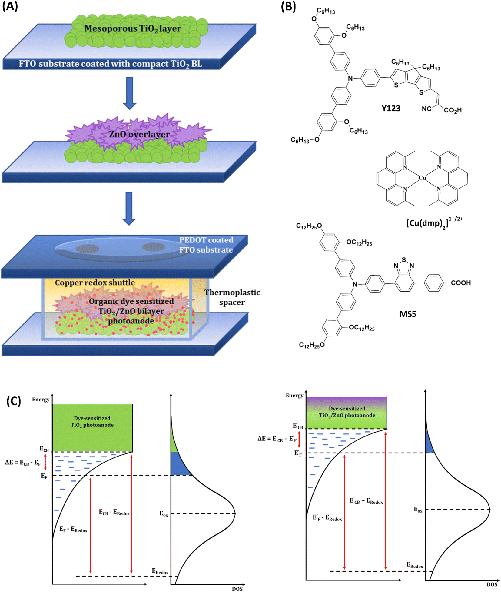 | ||
| Fig. 1 (A) Fabrication scheme and device architecture of DSCs employing bilayer TiO2/ZnO photoanodes. (B) Chemical structure of the organic sensitizers (Y123 and MS5) and the redox mediator ([Cu(dmp)2]1+/2+). (C) Alignment of energy levels of the semiconductor layer and electrolyte. A negative shift in the conduction band edge (ECB) of TiO2/ZnO electrodes results in reduced overlapping between the oxidized energy states of the electrolyte with the conduction band states (shaded in green) and the gap states (shaded in blue). | ||
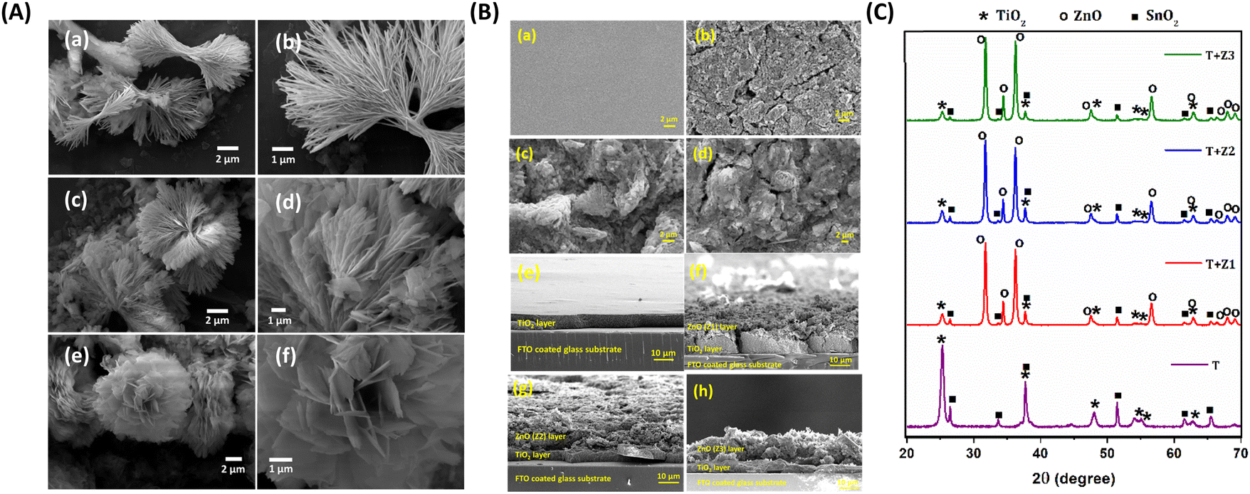 | ||
| Fig. 2 (A) SEM images of the as-synthesized samples of (a and b) mimosa flower-like microstructures (Z1); (c and d) dandelion flower-like microstructures (Z2); (e and f) rose flower-like microstructures (Z3). (B) SEM images of the top view of the photoanodes: (a) T, (b) T + Z1, (c) T + Z2, (d) T + Z3; and cross-sectional view of the photoanodes: (e) T, (f) T + Z1, (g) T + Z2, (h) T + Z3; and (C) XRD patterns of T, T + Z1, T + Z2 and T + Z3 layers coated over an FTO substrate. | ||
| Device code | Average layer thicknessa (μm) | Dye loading (mol cm−2) | V OC (V) | J SC (mA cm−2) | FFb | PCEb (%) | Integrated JSCc (mA cm−2) | α | n | V fb (V) |
|---|---|---|---|---|---|---|---|---|---|---|
a Average semiconductor layer thickness obtained from cross-sectional SEM analysis.
b
J–V parameters of champion cells and averages taken over five sets of samples (in parentheses) with a maximum mean deviation of ±0.01, ±0.31, ±0.02 and ±0.14 in VOC, JSC, FF and PCE respectively.
c
J
SC obtained by integrating the IPCE spectra.
d Obtained from the log![[thin space (1/6-em)]](https://www.rsc.org/images/entities/char_2009.gif) Cμversus VOC plot.
e Obtained from the VOCversus ϕ plot.
f Obtained from Mott–Schottky analysis. Cμversus VOC plot.
e Obtained from the VOCversus ϕ plot.
f Obtained from Mott–Schottky analysis.
|
||||||||||
| T | 6.3 | 0.94 × 10⁻⁷ | 1.02 (1.03) | 12.24 (12.01) | 0.64 (0.64) | 8.00 (7.92) | 11.60 | 0.11 | 2.51 | 0.69 |
| T + Z1 | 20.3 | 1.48 × 10⁻⁷ | 1.13 (1.13) | 9.88 (9.74) | 0.68 (0.68) | 7.61 (7.48) | 9.90 | 0.14 | 1.34 | 0.87 |
| T + Z2 | 21.5 | 1.43 × 10⁻⁷ | 1.11 (1.11) | 8.91 (9.04) | 0.67 (0.65) | 6.67 (6.60) | 9.60 | 0.13 | 1.50 | 0.81 |
| T + Z3 | 20.3 | 1.36 × 10⁻⁷ | 1.09 (1.09) | 8.63 (8.58) | 0.63 (0.62) | 5.96 (5.85) | 8.60 | 0.11 | 2.01 | 0.77 |
The current density versus voltage (J–V) curves for the standard device (T) along with the TiO2/ZnO bilayer devices (T + Z1, T + Z2 and T + Z3), measured under AM 1.5G simulated solar irradiation (100 mW cm−2), are given in Fig. 3(A), and the corresponding photovoltaic parameters are summarized in Table 1. The control device T with one layer of TiO2 exhibited a VOC of 1.02 V. With the introduction of a ZnO layer on top of TiO2, the VOC increased to 1.13 V, 1.11 V and 1.09 V for the T + Z1, T + Z2 and T + Z3 devices, respectively. Among the three bilayer devices, T + Z1 delivered the best photovoltaic performance of 7.61%, with a better VOC (1.13 V), JSC (9.88 mA cm−2) and FF (0.68). The IPCE spectra of the devices followed similar JSC trends (Fig. 3(B)) with matching values inside the permitted error limits for integrated JSC from IPCE, and JSC obtained from J–V measurements (Table 1). The observed blue shift in the IPCE spectra of T + Z devices, compared to the T device, can be ascribed to dye aggregation within the bilayer devices. On the other hand, the difference in onset of IPCE spectra between the different bilayer devices may be attributed to the difference in scattering effects caused by the utilization of various ZnO microstructure (Z1, Z2, and Z3) overlayers with varying particle size and layer thickness.
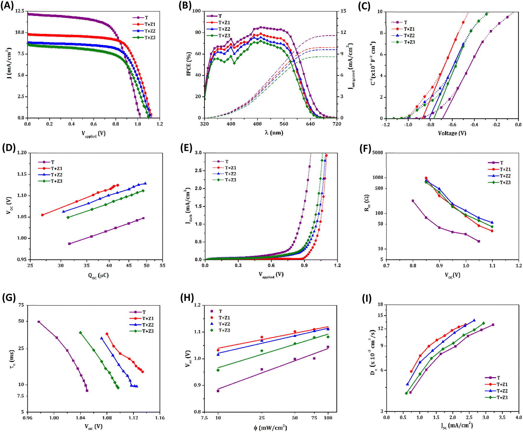 | ||
| Fig. 3 (A) The J–V curves measured under AM 1.5G 1 sun illumination (100 mW cm−2), (B) IPCE of the DSCs (the dotted line represents the integrated photocurrent density calculated from the IPCE and the standard solar emission spectrum), (C) Mott–Schottky (MS) plots, (D) charge extraction (CE) plots, (E) J–V curves measured in the dark, (F) charge transfer resistance (Rct) measured from EIS analysis under dark conditions plotted against corrected potential, (G) lifetime (τn) as a function of VOC obtained from transient photovoltage decay measurements, (H) intensity dependence plot of VOC, the solid line represents linear fits of the data and (I) diffusion coefficient (Dn) as a function of JSC. | ||
The flat band potentials (Vfb) of the semiconductor utilized in different devices were determined by extrapolating the linear region of the Mott–Schottky (MS) plots, as depicted in Fig. 3(C), to intersect the voltage axis.41–44 The obtained Vfb values for T + Z1, T + Z2, and T + Z3 are observed to be shifted towards more negative potentials compared to the standard T device (Table 1). This shift indicates that in the bilayer devices, specifically with the inclusion of a ZnO layer on top of the TiO2, the conduction band (CB) is shifted towards more negative potentials. It is well established that ZnO possesses a more negatively positioned CB edge relative to TiO2. Moreover, S.-S. Kim et al. have reported, based on cyclic voltametric studies, that the addition of ZnO to TiO2 results in a negative shift in the CB edge of TiO2.45 This upward shift in the CB can be attributed to the apparent charging of the ZnO layer due to the band alignment at the TiO2/ZnO interface.46,47 The negative shift in the CB for the TiO2/ZnO bilayer devices was further verified through charge extraction (CE) plots (Fig. 3(D)), which demonstrate an approximate 50–100 mV negative shift upon the introduction of ZnO layers. This negatively shifted CB may further contribute to the enhanced VOC in the TiO2/ZnO bilayer devices.
Electrochemical Impedance Spectroscopy (EIS) measurements were carried out to further investigate the charge carrier concentration in the bilayer devices and to probe recombination losses. The obtained Nyquist plots were fitted using a modified Randles circuit (Fig. S2(A), ESI†).48 The corresponding fitted parameters obtained at a bias of 1 V are listed in Table S2, ESI.† The chemical capacitance (Cμ) determined from EIS analysis plotted as a function of VOC, given in Fig. S2(B), ESI,† also shows a negative shift in the CB position for bilayer devices as observed previously from the MS and CE analysis. Cμ has an exponential dependence on VOC, as given by the relation,46,49
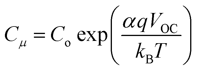 | (1) |
Cμversus VOC plot (Fig. S2(B), ESI†), and the obtained values (Table 1) showed a minimal difference between the standard and the bilayer devices. Hence, the variation in Cμ can be directly correlated with the shift in CB edges as per the relation,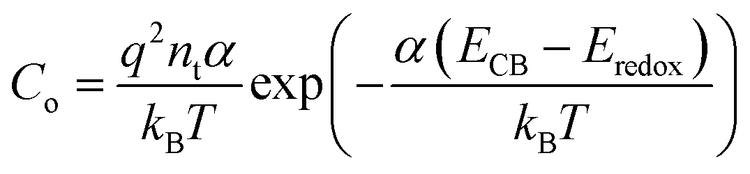 | (2) |
Empirically, the lower Cμ values for the bilayer devices (Fig. S2(B) and Table S2, ESI†) further substantiate the negative shift in CB.
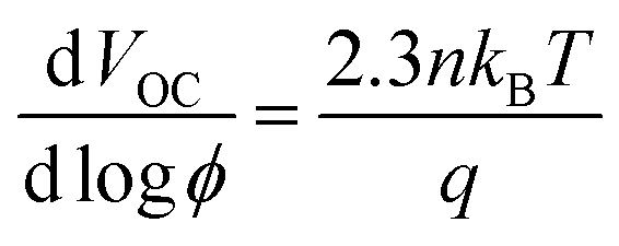
The negative shift in CB for the bilayer devices concomitantly reduces the overlap of the CB states and the sub-bandgap states/trap states of the semiconductor with the redox mediator's oxidized states, thereby suppressing electron transfer from the semiconducting layer to the electrolyte (Fig. 1(C)).50,51 This is evident from the lower dark current (Fig. 3(E)) and higher recombination resistance, Rct (Fig. 3(F) and Table S2, ESI†) for the TiO2/ZnO bilayer devices. The increased Rct in the bilayer devices can also be attributed to the formation of an energy barrier at the TiO2/ZnO interface, owing to the higher CB energy of ZnO.52 Altogether, these findings highlight the superior ability of the TiO2/ZnO bilayer devices to suppress charge recombination at the semiconductor/electrolyte interface compared to the standard TiO2 device. The charge carrier recombination losses were further studied by performing the transient photovoltage decay measurements, and the lifetime (τn) obtained as a function of VOC is provided in Fig. 3(G). Compared to the TiO2 alone device, the bilayer devices exhibited improved lifetime, again indicating efficient suppression of recombination. Notably, we observed the same trend in the lifetime for these devices by performing intensity modulated photovoltage spectroscopy (IMVS) measurements as well (Fig. S3(A), ESI†). Further, the role of trap states in the recombination was explored using intensity-dependent VOC measurements (Fig. 3(H)). The slope of the semi-logarithmic plot of VOCversus illumination intensity (ϕ) is used to estimate the ideality factor (n) of the devices using the equation,25,53
 | (3) |
The trap state-mediated recombination leads to non-linear recombination kinetics, which results in a deviation of n from the ideal value of unity. From the obtained values of n provided in Table 1, it is quite obvious that the trap state-assisted recombination is less for the bilayer devices; in particular, the T + Z1 device possesses an n value which is closer to unity. This explains our aforementioned notion that the negatively shifted CB in bilayer devices diminishes the electron transfer from the trap states to the electrolyte. Thus, the observed increase in VOC for the TiO2/ZnO bilayer devices can be predominantly associated with the collective effect of CB shift and suppressed recombination.
From Table S2, ESI,† it is observed that the resistance to the diffusion of redox species in the bulk of the electrolyte (Rd-bulk) is similar for all the devices, while that within the mesoporous layer (Rd-WE) is increased by more than three times for the TiO2/ZnO devices, owing to the higher layer thicknesses. In addition, the copper complex based electrolyte systems are reported to be mass transport limited. However, the similar current transient (CT) curves for T and T + Z devices under an illumination intensity of 100 mW cm−2 (Fig. S3(B), ESI†), and the linear nature of the JSCversus ϕ plots (Fig. S3(C), ESI†) for the T + Z devices indicates minimal influence of mass transport in these systems, despite the higher layer thickness. This may be attributed to the highly porous nature of the ZnO overlayer. Moreover, ZnO, being endowed with appreciable electron mobility, can act as an excellent electron transport layer in the DSC. Resultantly, the T + Z devices having ZnO overlayers exhibit better diffusion coefficients (Dn), when compared to the T device (as shown in Fig. 3(I)). Nonetheless, the JSC of T + Z devices is lower than that of T devices, which may be explained by the lower injection driving force associated with the upward-shifted CB edges in the bilayer devices. Further, the presence of Zn2+/dye aggregates within the ZnO layer, due to degradation of ZnO under acidic conditions, may also play a role in the injection challenges observed in the TiO2/ZnO bilayer devices.54,58,59 The comprehensive investigation mentioned above, encompassing diverse interfacial charge transfer studies in both standard and bilayer devices, establishes a clear correlation with the disparities observed in photovoltaic parameters between the two device configurations.
Among the bilayer devices, T + Z1 delivered the best performance with a ca. 15 μm thick ZnO (Z1) layer over TiO2 (Fig. 2B(f)). The effect of ZnO layer thickness on device performance was further investigated by fabricating T + Z1 devices with an average Z1 layer thickness of 5 μm, 15 μm and 25 μm (Fig. S4, ESI†). The obtained J–V curves under AM 1.5G 100 mW cm−2 illumination are shown in Fig. S5, ESI† and the photovoltaic parameters are summarized in Table S3, ESI.† The variation of ZnO layer thickness did not bring much difference in the photovoltaic parameters (Fig. 4(A)); however, a thickness of 15 μm was found to be optimal, giving the highest VOC and optimum PCE. A more negatively shifted CB edge (Fig. 4(B)) and higher Dn (Fig. 4(C)) contributed to the better performance of T + Z1 devices with a 15 μm thick Z1 layer.
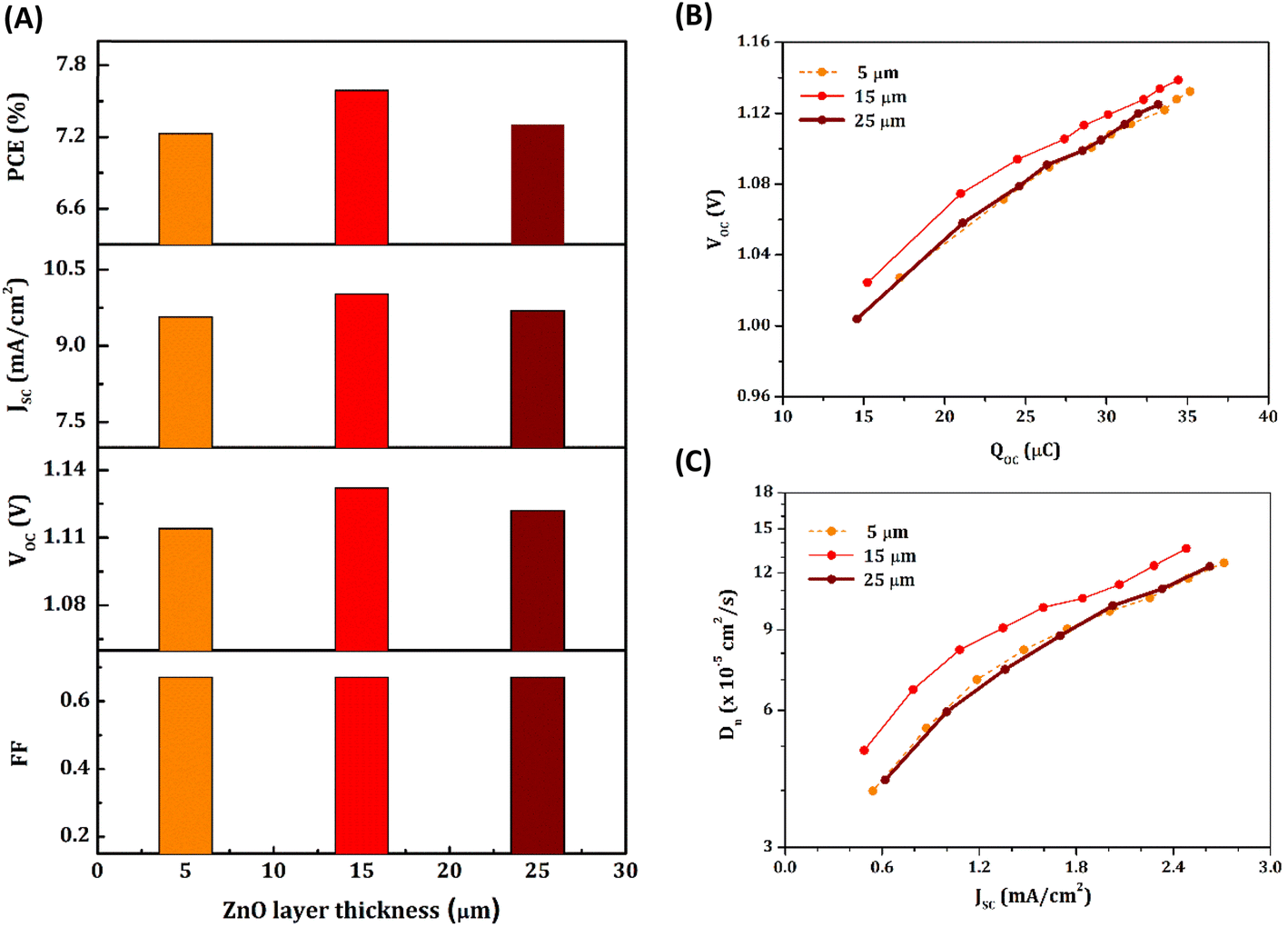 | ||
| Fig. 4 (A) Comparison of photovoltaic parameters (JSC, VOC, FF and PCE) of T + Z1 devices with different ZnO layer thicknesses. (B) VOC as a function of extracted charge and (C) diffusion coefficient (Dn) as a function of JSC obtained for T + Z1 devices with different ZnO layer thicknesses. | ||
Compact blocking layers (BLs) play a critical role in inhibiting leakage/recombination in DSCs, particularly employing bulky alternate metal complex redox mediators.55,56 The conventional method of depositing TiO2 BLs by TiCl4 treatment causes damage to the ZnO overlayers. Therefore, an ultrathin TiO2 BL was introduced over the bilayer architecture using commercial BL solution as described in the Experimental section, ESI.† Under AM 1.5G 100 mW cm−2 illumination, the bilayer devices with BL (T + Z1 + BL) fabricated using the Y123 sensitizer and [Cu(dmp)2]1+/2+ redox electrolyte delivered a PCE of 8.16% with VOC of 1.12 V, JSC of 10.29 mA cm−2 and FF of 0.70 (Fig. 5(A) and Table 2). Slightly improved JSC and FF were realized for the T + Z1 + BL device compared to T + Z1 (without BL) with a minor drop in VOC. Introduction of BLs resulted in a positive shift in CB, as evident from the CE plot (Fig. 5(B)), leading to a lower VOC. Additionally, this increases the overlap of CB states with the oxidized states in the redox system, which results in more recombination as observed from transient photovoltage decay (Fig. 5(C)), OCVD (Fig. S6(A), ESI†) and IMVS (Fig. S6(B), ESI†) measurements. On the other hand, the introduction of BL successfully inhibited electron leakage at the FTO/electrolyte interface, as reflected in the dark J–V plot (Fig. 5(D)), leading to better FF. It is already known that multiple trapping–detrapping events slow down the diffusion of charge carriers in semiconducting films.57 The TiO2 BL could efficiently passivate these traps in the TiO2/ZnO bilayer devices, reducing the transport time (τd) (Fig. S6(C), ESI†). This in turn contributes to enhanced Dn (Fig. 5(E)), leading to improved JSC, which is reflected in the IPCE plot (Fig. S6(D), ESI†) and integrated JSC values (Table 2), resulting in improved PCE for the T + Z1 + BL device.
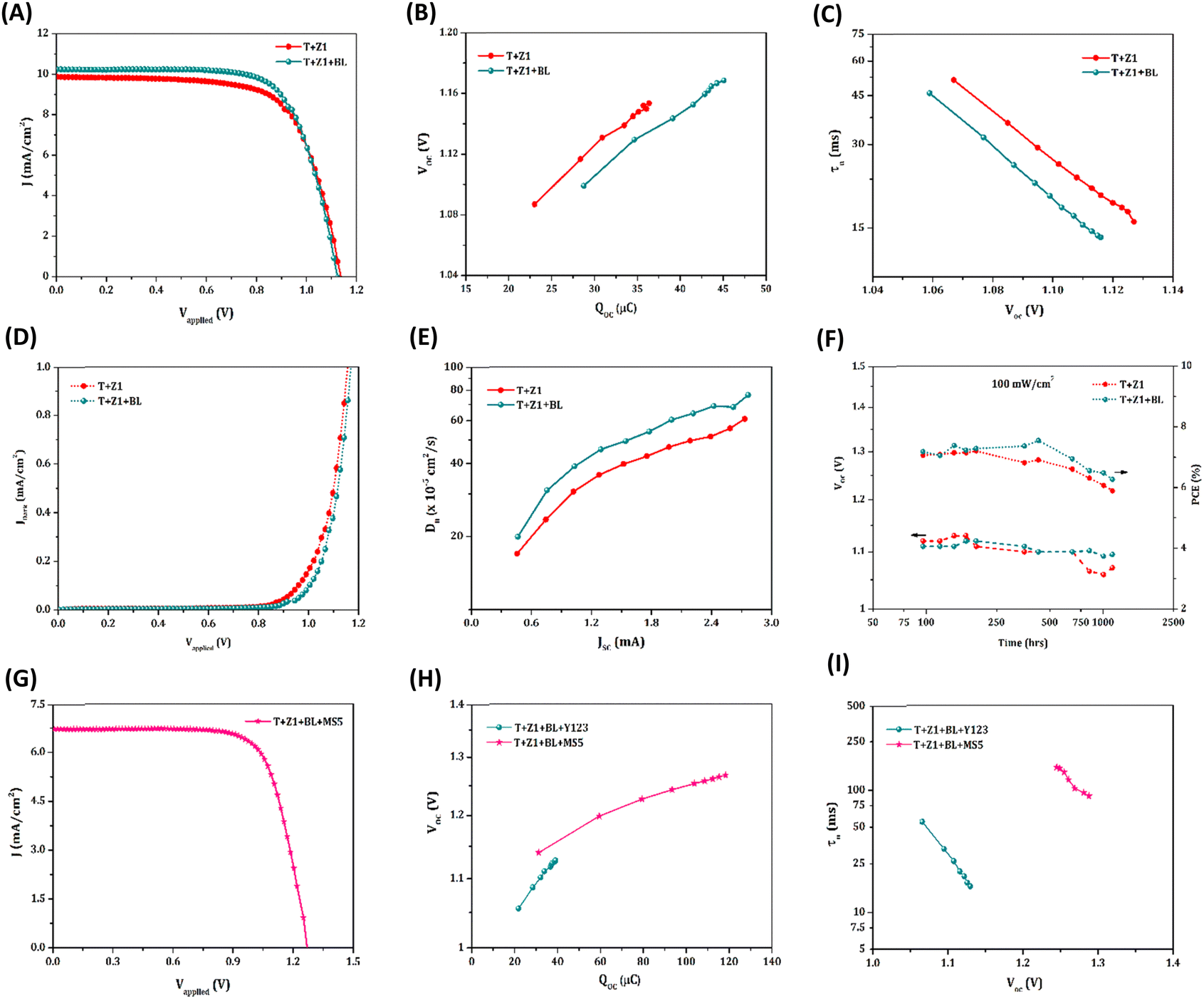 | ||
| Fig. 5 (A) J–V curves measured under AM 1.5G 1 sun illumination (100 mW cm−2), (B) charge extraction (CE) plots, (C) lifetime (τn) as a function of VOC obtained from transient photovoltage decay measurements, (D) J–V characteristics obtained under dark conditions, (E) diffusion coefficient (Dn) as a function of JSC obtained from transient photocurrent decay measurements and (F) stability data obtained for TiO2/ZnO bilayer DSCs with a blocking layer (T + Z1 + BL) and without the blocking layer (T + Z1), employing the Y123 sensitizer and [Cu(dmp)2]1+/2+ redox shuttle. (G) J–V curves measured under AM 1.5G 1 sun illumination (100 mW cm−2) for TiO2/ZnO bilayer DSCs with BL (T + Z1 + BL) employing the MS5 sensitizer and [Cu(dmp)2]1+/2+ redox electrolyte. (H) Charge extraction (CE) and (I) lifetime (τn) plots, obtained for TiO2/ZnO bilayer DSCs with BL (T + Z1 + BL) employing Y123 and MS5 sensitizers and the [Cu(dmp)2]1+/2+ redox electrolyte. | ||
| Device code | V OC (V) | J SC (mA cm−2) | FFa | PCEa (%) | Integrated JSCb (mA cm−2) |
|---|---|---|---|---|---|
| a J–V parameters of champion cells and averages taken over five sets of samples (in parentheses) with a maximum mean deviation of ±0.01, ±0.30, ±0.02 and ±0.15 in VOC, JSC, FF and PCE, respectively. b J SC obtained by integrating the IPCE spectra. | |||||
| T + Z1 + BL + Y123 | 1.12 (1.12) | 10.29 (10.33) | 0.70 (0.70) | 8.16 (8.12) | 10.20 |
| T + Z1 + BL + MS5 | 1.27 (1.26) | 6.75 (6.70) | 0.73 (0.72) | 6.23 (6.08) | 7.30 |
As emphasized in the introduction section, ZnO possesses advantages such as wider bandgap and higher electron mobility. However, its lower electrochemical stability under the working conditions of the solar cell, along with the presence of defects and trap states, contributes to more recombination and reduces the long-term stability of the ZnO based devices. Two major degradation mechanisms contribute to the reduction in performance of ZnO based DSCs. Firstly, when ZnO electrodes are immersed in the acidic dye solution for dye adsorption, the Zn2+ ions from the ZnO surface dissolve, forming Zn2+/dye aggregates that become trapped within the pores of the ZnO matrix. This limits electron injection and reduces the JSC of the device.58 Secondly, ZnO undergoes chemical degradation under illumination in the presence of electrolyte, releasing Zn2+ and O2− ions along with desorbed dye molecules into the electrolyte.59 This leads to a reduced number of adsorbed dye molecules, formation of defects on the ZnO surface, and aggregation of the dye, thereby affecting the JSC and PCE of the device. In our study, we successfully addressed the first degradation process by introducing the TiO2 BL over the ZnO film. This is evident from the improved JSC observed for the T + Z1 + BL device compared to the T + Z1 device, despite the reduced dye loading in the T + Z1 + BL film (1.2 × 10⁻⁷ mol cm−2), indicating reduced dye aggregation. Additionally, the introduction of the BL slowed down the rate of the second degradation process, as observed in the stability measurements (Fig. 5(F)). While the bare T + Z1 device experienced a drop in both the VOC and PCE after 200 hours, the T + Z1 + BL device retained approximately 98% of the initial VOC even after 1000 hours. However, the PCE of the devices began to decrease after 400 hours.
SEM and XRD analysis were carried out to identify the changes in the bilayer photoanode films during the stability test. The SEM images of T + Z1 and T + Z1 + BL electrodes after exposure to the electrolyte for over 1000 hours are presented in Fig. S7(A).† These images reveal an increased presence of cracks compared to the fresh electrode. Additionally, after prolonged contact with the electrolyte, both films exhibited a smoother surface compared to the fresh T + Z1 films. This can be attributed to the selective dissolution of ZnO from the film surface.60 XRD patterns of the Y123 dye adsorbed T + Z1 and T + Z1 + BL electrodes after 1000 hours of electrolyte soaking are shown in Fig. S7(B).† The corroded ZnO films still exhibited a crystalline nature, although some peak intensities, such as [100], [101], and [110], were reduced compared to the fresh T + Z1 films (Fig. 2(C)). However, no shift in peak positions or appearance of new peaks was observed in the XRD spectra of the degraded films. Hence, prolonged exposure to the electrolyte does not affect the crystallinity of the ZnO films but induces changes in the film surface due to the degradation of ZnO in both the bilayer electrodes with and without the BL.61 In conclusion, the exposure of the bilayer films to the electrolyte system for a long time, coupled with frequent illumination, likely resulted in the dissolution of ZnO and dye into the electrolyte, which might have led to a decrease in JSC and hence PCE of the T + Z1 + BL devices after 400 hours (as seen in Fig. 5(F)).
Eventually, by sensitizing our best-optimized bilayer architecture (T + Z1 + BL) with MS5 dye, we could realize a record VOC of 1.27 V (previous best – 1.24 V)26 under AM 1.5G solar illumination with a JSC of 6.75 mA cm−2, FF of 0.73 and PCE of 6.23% (Fig. 5(G) and Table 2). The JSC obtained by integrating the corresponding IPCE spectrum (Fig. S8(A), ESI†) matches the observed JSC within the permitted error limits. Switching the dye from the conventional Y123 to MS5 contributed to the negative shift in CB (Fig. 5(H)) and couple of orders of magnitude improvement in lifetime (Fig. 5(I)) owing to the retardation of recombination by the long alkyl chains present in the MS5 sensitizer. The MS5 sensitized T + Z1 + BL bilayer device could also achieve a VOC of 1.295 V under a higher-intensity LED illumination of 200 mW cm−2 (Fig. S8(B), ESI†).
DSCs proved to be among the most efficient indoor/ambient light harvesting PV technologies. The potential of the newly designed bilayer devices was tested under warm white CFL, and daylight LED illumination. Fig. S10, ESI† shows the custom-designed indoor PV characterization set-up and Fig. S11, ESI† shows the spectral irradiance and integrated power under 1000 lux and 500 lux CFL/LED illumination. The energy harvesting and management circuits in most IoT smart device applications demand higher open circuit potentials. By using the TiO2/ZnO bilayer architecture along with Y123 dye and [Cu(dmp)2]1+/2+, we were able to realize an improvement in VOC both under CFL and LED illumination (Fig. 6(A, B) and Table 3). Under 1000 lux CFL illumination, the T + Z1 device exhibited a VOC of 1.0 V (with a JSC of 78.7 μA cm−2, FF of 0.75, PCE of 20.9% and a maximum power output (Pmax) of 59.3 μW cm−2) compared to a VOC of 0.82 V for the standard T device (with a JSC of 103.9 μA cm−2, FF of 0.70, PCE of 21.2% and Pmax of 60.1 μW cm−2). Careful use of BLs further increased the current density without compromising the FF. Thus T + Z1 + BL devices delivered similar PCE (21.3%) and Pmax (60.3 μW cm−2) to those of the control T device, with a 20.7% improvement in VOC (0.99 V). Similar trends were observed under lower illumination intensity of 500 lux, where VOC improved from 0.79 V for T to 0.96 V for T + Z1 + BL devices, along with improvement in FF, PCE and Pmax.
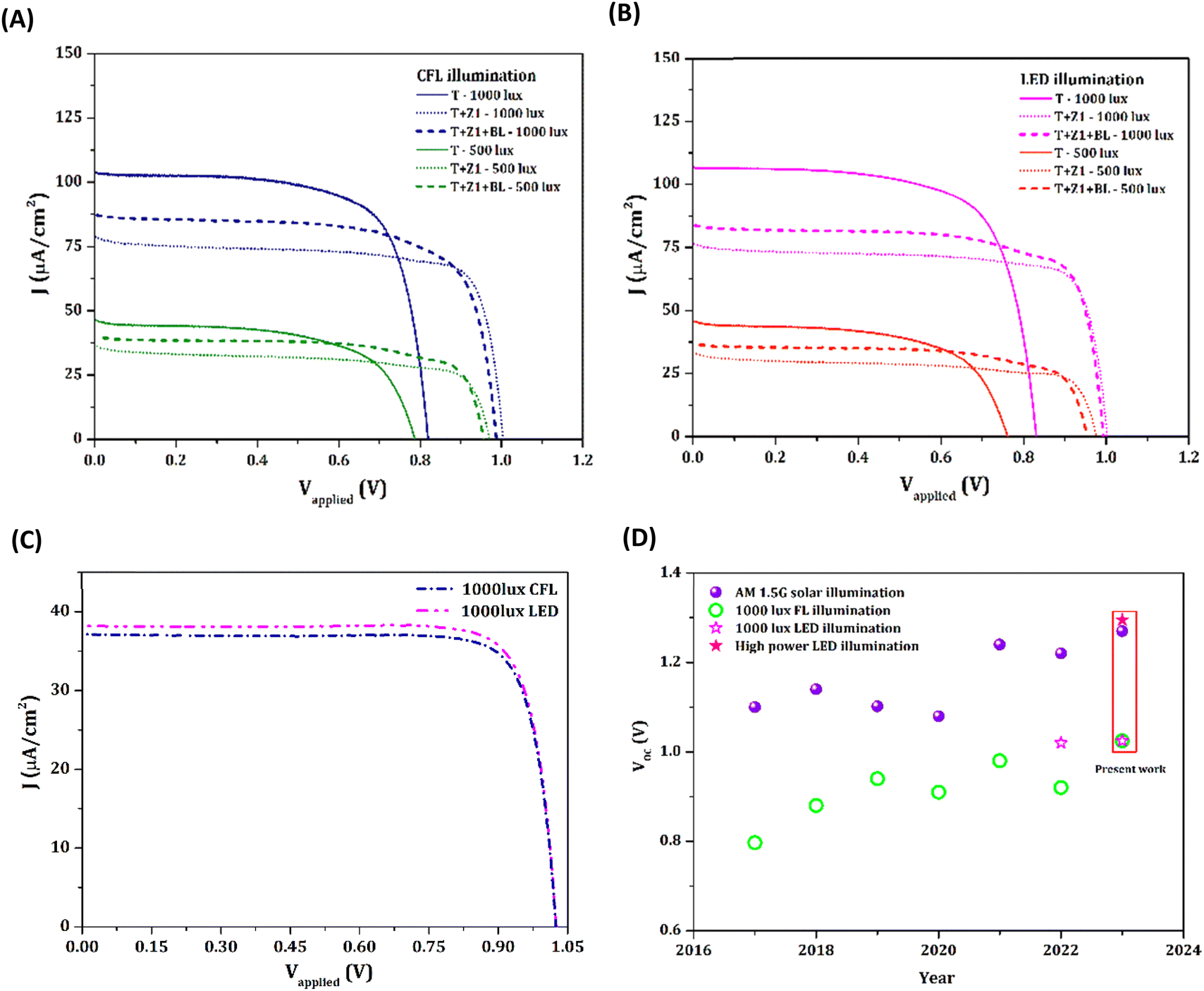 | ||
| Fig. 6 (A) J–V curves measured for T, T + Z1 and T + Z1 + BL DSCs employing the Y123 sensitizer and [Cu(dmp)2]1+/2+ redox electrolyte under 1000 lux and 500 lux CFL illumination. (B) J–V curves measured for T, T + Z1 and T + Z1 + BL DSCs employing the Y123 sensitizer and [Cu(dmp)2]1+/2+ redox electrolyte under 1000 lux and 500 lux LED illumination. (C) J–V curves measured for T + Z1 + BL DSCs employing the MS5 sensitizer and [Cu(dmp)2]1+/2+ redox electrolyte under 1000 lux CFL and LED illumination (obtained PV parameters are shown in the inset), and (D) representation of the highest VOC values reported in the literature yearly (since 2017) for DSCs using organic dyes and copper electrolyte under outdoor and indoor illumination. | ||
| Illumination source | Intensity | P in (μW cm−2) | Device code | V OC (V) | J SC (μA cm−2) | FFa | PCEa (%) | P max (μW cm−2) |
|---|---|---|---|---|---|---|---|---|
| a J–V parameters of champion cells and averages taken over five sets of samples (in parentheses) with a maximum mean deviation of ±0.01, ±3.2, ±0.02, ±0.5 and ±1.5 in VOC, JSC, FF, PCE and Pmax respectively. | ||||||||
| CFL | 1000 lux | 283 | T | 0.82 (0.81) | 103.9 (102.5) | 0.70 (0.70) | 21.2 (21.0) | 60.1 (59.6) |
| T + Z1 | 1.00 (0.99) | 78.7 (82.6) | 0.75 (0.73) | 20.9 (20.5) | 59.3 (58.1) | |||
| T + Z1 + BL | 0.99 (0.98) | 87.4 (86.4) | 0.70 (0.70) | 21.3 (21.1) | 60.3 (59.7) | |||
| 500 lux | 143 | T | 0.79 (0.78) | 46.0 (45.4) | 0.60 (0.60) | 15.2 (14.8) | 21.9 (21.1) | |
| T + Z1 | 0.97 (0.97) | 36.6 (35.8) | 0.65 (0.64) | 16.2 (15.8) | 23.2 (22.5) | |||
| T + Z1 + BL | 0.96 (0.95) | 40.8 (40.6) | 0.63 (0.63) | 17.5 (17.0) | 25.8 (24.3) | |||
| LED | 1000 lux | 313 | T | 0.83 (0.83) | 106.7 (107.2) | 0.70 (0.70) | 19.9 (19.8) | 62.2 (61.9) |
| T + Z1 | 1.00 (1.00) | 77.1 (76.4) | 0.76 (0.76) | 18.8 (18.6) | 58.9 (58.2) | |||
| T + Z1 + BL | 0.99 (0.99) | 84.6 (84.1) | 0.73 (0.72) | 19.7 (19.3) | 61.6 (60.3) | |||
| 500 lux | 156 | T | 0.76 (0.76) | 46.3 (45.6) | 0.60 (0.60) | 13.6 (13.4) | 21.2 (21.1) | |
| T + Z1 | 0.98 (0.97) | 33.5 (33.3) | 0.67 (0.65) | 14.0 (13.6) | 21.8 (21.2) | |||
| T + Z1 + BL | 0.95 (0.95) | 36.9 (37.3) | 0.66 (0.63) | 14.9 (14.4) | 23.3 (22.4) | |||
Under 1000 lux LED illumination, the T + Z1 device delivered a VOC of 1.0 V (JSC = 77.1 μA cm−2, FF = 0.76, PCE = 18.8% and Pmax = 58.9 μW cm−2) compared to a VOC of 0.83 V for the standard T device (JSC = 106.7 μA cm−2, FF = 0.70, PCE = 19.9% and Pmax = 62.2 μW cm−2). Using T + Z1 + BL, the current density was further improved to achieve a Pmax (61.6 μW cm−2) similar to that of T, but with 19.3% increased VOC (0.99 V). Under 500 lux LED illumination, VOC increased from 0.76 V for T to 0.98 V for T + Z1. The T + Z1 + BL device could further improve the JSC and PCE, leading to improved power output, without compromising much on the VOC. The performance of T + Z1 + BL devices employing MS5 dye and [Cu(dmp)2]1+/2+ electrolyte was also evaluated under indoor light, and they delivered a record VOC of 1.025 V under both 1000 lux LED and 1000 lux CFL illumination (Fig. 6(C) and Table S4†). However, the PCE was lower than for the devices fabricated using the Y123 sensitizer due to the loss in JSC, which could be attributed to the narrower absorption window of MS5 dye. Fig. 6(D) and Table S5† represent the highest VOC values reported in the literature yearly (since 2017) for DSCs using organic dyes and copper electrolyte under outdoor and indoor illumination. The champion VOC of 1.27 V under one sun, 1.295 V under higher intensity (200 mW cm−2) LED light and 1.025 V under 1000 lux CFL and LED illumination are the best open circuit potentials in DSCs reported to date. Ultimately, we could highlight the significance of this work by powering a temperature sensor (ACETEQ DC-2) completely autonomously using a single DSC (of active area 0.24 cm2) employing a TiO2/ZnO bilayer photoanode sensitized with MS5 dye (eliminating the need for co-sensitization) and [Cu(dmp)2]1+/2+ electrolyte, under CFL (Video S1†) as well as LED lighting conditions (Video S2 and Fig. S12, ESI†). The present design approach has been successful in developing indoor DSCs with smaller footprints contributing to reduced costs and higher open circuit potentials that enable better integration possibilities to realize self-powered IoT devices.
3. Conclusions
In summary, we present a novel architecture for dye-sensitized solar cells (DSCs), which involves the implementation of a layer of ZnO hierarchical microstructures over the conventional TiO2 active layer, resulting in a TiO2/ZnO bilayer photoanode. Our design aims to enhance the open-circuit voltage (VOC) of DSCs under one sun and indoor lighting conditions. Using an optimized bilayer electrode with a blocking layer (T + Z1 + BL) in combination with an MS5 sensitizer and [Cu(dmp)2]1+/2+ redox electrolyte, we have achieved a remarkable VOC of 1.27 V under AM 1.5G one sun illumination and 1.295 V under a higher intensity LED light of 200 mW cm−2, which are the highest VOC reported to date for a single junction DSC. Detailed interfacial charge transfer studies have revealed that the bilayer structure leads to a negatively shifted conduction band and improved electron lifetime, contributing significantly to the enhanced VOC. We have also succeeded in achieving a VOC of 1.025 V under both 1000 lux CFL and LED illumination using the MS5 sensitizer and [Cu(dmp)2]1+/2+ redox electrolyte employing the TiO2/ZnO bilayer photoanode (T + Z1 + BL). These promising results have inspired us to develop a battery-free temperature sensor that can be powered autonomously by a single DSC of 0.24 cm2 active area under indoor illumination. Overall, this work provides valuable material and device engineering strategies that can be used to realize higher VOC in conjunction with the appropriate combination of dyes and electrolytes. Achieving higher VOC is essential for operating innovative self-powered electronic applications. The majority of the energy harvesting and management circuits used in these smart devices require lower current (in μA) but demand higher voltage (above 1 V) for continuous operation, highlighting the fact that more than current and efficiency, VOC needs to be taken into consideration while designing DSCs for indoor photovoltaic applications. Furthermore, reducing the device's footprint without compromising the voltage opens up creative and imaginative possibilities for integrating indoor DSCs as a replacement for batteries contributing to carbon neutrality and sustainability.Author contributions
SS conceived the idea and coordinated the work. AJ synthesized the materials, carried out all of the characterization, fabricated the solar cells and conducted measurements and data analysis under one sun and indoor conditions. GV performed the SEM measurements. PSD and KNNU contributed to manuscript corrections and preparation. SS wrote the manuscript with support from AJ and revisions from other co-authors. All authors commented on the manuscript.Conflicts of interest
There are no conflicts to declare.Acknowledgements
We acknowledge financial support from the SERB CRG project (CRG/2020/001406), CSIR-FIRST project (MLP65), DST Solar Challenge Award (DST/ETC/CASE/RE5/2023/05 (C)), CSIR-FTT project (MLP74) and CSIR-Misson Project (HCP30). GV gratefully acknowledges financial support from DST-TRC (AI/1/65/ARCI/2014). AJ acknowledges CSIR for the research fellowship. AJ acknowledges support from Mr Sourava Chandra Pradhan in optimizing the copper electrolyte-based DSCs and Ms Sreelekshmy M. R. for support with device fabrication and measurements.References
- J. Gubbi, R. Buyya, S. Marusic and M. Palaniswami, Future Gener. Comput. Syst., 2013, 29, 1645–1660 CrossRef.
- M. Mohammadi and A. Al-Fuqaha, IEEE Commun. Mag., 2018, 56, 94–101 Search PubMed.
- D. Ma, G. Lan, M. Hassan, W. Hu and S. K. Das, IEEE Commun. Surv. Tutor., 2020, 22, 1222–1250 Search PubMed.
- J. Hester and J. Sorber, in SenSys 2017 – Proceedings of the 15th ACM Conference on Embedded Networked Sensor Systems, Association for Computing Machinery, Inc., 2017, vol. 2017 Search PubMed.
- H. Elahi, K. Munir, M. Eugeni, S. Atek and P. Gaudenzi, Energies, 2020, 13, 5528 CrossRef CAS.
- A. Aslam, U. Mehmood, M. H. Arshad, A. Ishfaq, J. Zaheer, A. Ul Haq Khan and M. Sufyan, Sol. Energy, 2020, 207, 874–892 CrossRef CAS.
- G. Gokul, S. C. Pradhan and S. Soman, Energy Environ. Sustain., 2019, 281–316 Search PubMed.
- Y. Cao, Y. Liu, S. M. Zakeeruddin, A. Hagfeldt and M. Grätzel, Joule, 2018, 2, 1108–1117 CrossRef CAS.
- H. Michaels, M. Rinderle, R. Freitag, I. Benesperi, T. Edvinsson, R. Socher, A. Gagliardi and M. Freitag, Chem. Sci., 2020, 11, 2895–2906 RSC.
- M. Freitag, J. Teuscher, Y. Saygili, X. Zhang, F. Giordano, P. Liska, J. Hua, S. M. Zakeeruddin, J. E. Moser, M. Grätzel and A. Hagfeldt, Nat. Photonics, 2017, 11, 372–378 CrossRef CAS.
- B. O'Regan and M. Grätzel, Nature, 1991, 353, 737–740 CrossRef.
- A. Hagfeldt, G. Boschloo, L. Sun, L. Kloo and H. Pettersson, Chem. Rev., 2010, 110, 6595–6663 CrossRef CAS PubMed.
- A. R. Yugis, R. F. Mansa and C. S. Sipaut, IOP Conf. Ser.: Mater. Sci. Eng., 2015, 78, 012003 Search PubMed.
- F. Schoden, A. K. Schnatmann, E. Davies, D. Diederich, J. L. Storck, D. Knefelkamp, T. Blachowicz and E. Schwenzfeier-Hellkamp, Materials, 2021, 14, 6622 CrossRef CAS PubMed.
- F. Schoden, A. K. Schnatmann, T. Blachowicz, H. Manz-Schumacher and E. Schwenzfeier-Hellkamp, Sustainability, 2022, 14, 15280 CrossRef CAS.
- A. Dewan, S. U. Ay, M. N. Karim and H. Beyenal, J. Power Sources, 2014, 245, 129–143 CrossRef CAS.
- H. Jayakumar, K. Lee, W. S. Lee, A. Raha, Y. Kim and V. Raghunathan, Proceedings of the International Symposium on Low Power Electronics and Design, 2015, pp. 375–380 Search PubMed.
- X. Cao, Y. Xiong, J. Sun, X. Zhu, Q. Sun and Z. L. Wang, Adv. Funct. Mater., 2021, 31, 210298 Search PubMed.
- S. M. Feldt, G. Wang, G. Boschloo and A. Hagfeldt, J. Phys. Chem. C, 2011, 115, 21500–21507 CrossRef CAS.
- J. H. Yum, E. Baranoff, F. Kessler, T. Moehl, S. Ahmad, T. Bessho, A. Marchioro, E. Ghadiri, J. E. Moser, C. Yi, M. K. Nazeeruddin and M. Grätzel, Nat. Commun., 2012, 3, 631 CrossRef PubMed.
- Y. Saygili, M. Söderberg, N. Pellet, F. Giordano, Y. Cao, A. B. Munoz-García, S. M. Zakeeruddin, N. Vlachopoulos, M. Pavone, G. Boschloo, L. Kavan, J. E. Moser, M. Grätzel, A. Hagfeldt and M. Freitag, J. Am. Chem. Soc., 2016, 138, 15087–15096 CrossRef CAS PubMed.
- Y. Saygili, M. Stojanovic, H. Michaels, J. Tiepelt, J. Teuscher, A. Massaro, M. Pavone, F. Giordano, S. M. Zakeeruddin, G. Boschloo, J. E. Moser, M. Grätzel, A. B. Muñoz-García, A. Hagfeldt and M. Freitag, ACS Appl. Energy Mater., 2018, 1, 4950–4962 CrossRef CAS.
- Y. Ren, D. Zhang, J. Suo, Y. Cao, F. T. Eickemeyer, N. Vlachopoulos, S. M. Zakeeruddin, A. Hagfeldt and M. Grätzel, Nature, 2023, 613, 60–65 CrossRef CAS PubMed.
- A. Grobelny, Z. Shen, F. T. Eickemeyer, N. F. Antariksa, S. Zapotoczny, S. M. Zakeeruddin and M. Grätzel, Adv. Mater., 2023, 35, 2207785 CrossRef CAS PubMed.
- S. C. Pradhan, A. Hagfeldt and S. Soman, J. Mater. Chem. A, 2018, 6, 22204–22214 RSC.
- D. Zhang, M. Stojanovic, Y. Ren, Y. Cao, F. T. Eickemeyer, E. Socie, N. Vlachopoulos, J. E. Moser, S. M. Zakeeruddin, A. Hagfeldt and M. Grätzel, Nat. Commun., 2021, 12, 1777 CrossRef CAS PubMed.
- Q. Zhang and G. Cao, Nano Today, 2011, 6, 91–109 CrossRef CAS.
- J. A. Anta, E. Guillén and R. Tena-Zaera, J. Phys. Chem. C, 2012, 116, 11413–11425 CrossRef CAS.
- C. C. Raj and R. Prasanth, J. Power Sources, 2016, 317, 120–132 CrossRef CAS.
- S. H. Ko, D. Lee, H. W. Kang, K. H. Nam, J. Y. Yeo, S. J. Hong, C. P. Grigoropoulos and H. J. Sung, Nano Lett., 2011, 11, 666–671 CrossRef CAS PubMed.
- R. Gao, Z. Liang, J. Tian, Q. Zhang, L. Wang and G. Cao, Nano Energy, 2013, 2, 40–48 CrossRef CAS.
- W. Peng, L. Han and Z. Wang, Chem.–Eur. J., 2014, 20, 8483–8487 CrossRef CAS PubMed.
- S. Sasidharan, S. Soman, S. C. Pradhan, K. N. N. Unni, A. A. P. Mohamed, B. N. Nair and H. U. N. Saraswathy, New J. Chem., 2017, 41, 1007–1016 RSC.
- N. Memarian, I. Concina, A. Braga, S. M. Rozati, A. Vomiero and G. Sberveglieri, Angew. Chem., 2011, 123, 12529–12533 CrossRef.
- A. K. Chandiran, M. Abdi-Jalebi, M. K. Nazeeruddin and M. Grätzel, ACS Nano, 2014, 8, 2261–2268 CrossRef CAS PubMed.
- E. Guillén, L. M. Peter and J. A. Anta, J. Phys. Chem. C, 2011, 115, 22622–22632 CrossRef.
- K. Keis, J. Lindgren, S. E. Lindquist and A. Hagfeldt, Langmuir, 2000, 16, 4688–4694 CrossRef CAS.
- M. Quintana, T. Marinado, K. Nonomura, G. Boschloo and A. Hagfeldt, J. Photochem. Photobiol., A, 2009, 202, 159–163 CrossRef CAS.
- S. Sasidharan, A. Jagadeesh, S. C. Pradhan, B. N. Nair, A. Azeez Peer Mohamed, K. N. Narayanan Unni, S. Soman and U. Nair Saraswathy Hareesh, Sol. Energy, 2021, 226, 214–224 CrossRef CAS.
- N. T. K. Thanh, N. Maclean and S. Mahiddine, Chem. Rev., 2014, 114, 7610–7630 CrossRef CAS PubMed.
- K. Gelderman, L. Lee and S. W. Donne, J. Chem. Educ., 2007, 84, 685–688 CrossRef CAS.
- A. Gopalraman, S. Karuppuchamy and S. Vijayaraghavan, RSC Adv., 2019, 9, 40292–40300 RSC.
- J. Zhang and H. Yu, J. Mater. Chem. A, 2021, 9, 4138–4149 RSC.
- J. Zhang, Y. Sun, C. Huang, B. Yu and H. Yu, Adv. Energy Mater., 2022, 12, 2202542 CrossRef CAS.
- S. S. Kim, J. H. Yum and Y. E. Sung, Sol. Energy Mater. Sol. Cells, 2003, 79, 495–505 CrossRef CAS.
- S. Borbón, S. Lugo, D. Pourjafari, N. Pineda Aguilar, G. Oskam and I. López, ACS Omega, 2020, 5, 10977–10986 CrossRef PubMed.
- K. Shen, K. Wu and D. Wang, Mater. Res. Bull., 2014, 51, 141–144 CrossRef CAS.
- R. Ruess, S. Haas, A. Ringleb and D. Schlettwein, Electrochim. Acta, 2017, 258, 591–598 CrossRef CAS.
- F. Fabregat-Santiago, G. Garcia-Belmonte, I. Mora-Seró and J. Bisquert, Phys. Chem. Chem. Phys., 2011, 13, 9083–9118 RSC.
- S. Rühle, M. Greenshtein, S. G. Chen, A. Merson, H. Pizem, C. S. Sukenik, D. Cahen and A. Zaban, J. Phys. Chem. B, 2005, 109, 18907–18913 CrossRef PubMed.
- P. Siva Gangadhar, A. Jagadeesh, A. S. George, G. Reddy, S. Prasanthkumar, S. Soman and L. Giribabu, Mol. Syst. Des. Eng., 2021, 6, 779–789 RSC.
- K. E. Kim, S. R. Jang, J. Park, R. Vittal and K. J. Kim, Sol. Energy Mater. Sol. Cells, 2007, 91, 366–370 CrossRef CAS.
- P. Salvador, M. G. Hidalgo, A. Zaban and J. Bisquert, J. Phys. Chem. B, 2005, 109, 15915–15926 CrossRef CAS PubMed.
- K. Keis, E. Magnusson, H. Lindström, S. E. Lindquist and A. Hagfeldt, Sol. Energy Mater. Sol. Cells, 2002, 73, 51–58 CrossRef.
- H. Yu, S. Zhang, H. Zhao, G. Will and P. Liu, Electrochim. Acta, 2009, 54, 1319–1324 CrossRef CAS.
- I. P. Liu, W. H. Lin, C. M. Tseng-Shan and Y. L. Lee, ACS Appl. Mater. Interfaces, 2018, 10, 38900–38905 CrossRef CAS PubMed.
- T. Pauporté and C. Magne, Thin Solid Films, 2014, 560, 20–26 CrossRef.
- K. Keis, J. Lindgren, S. E. Lindquist and A. Hagfeldt, Langmuir, 2000, 16, 4688–4694 CrossRef CAS.
- L. Ke, S. Bin Dolmanan, L. Shen, P. K. Pallathadk, Z. Zhang, D. M. Ying Lai and H. Liu, Sol. Energy Mater. Sol. Cells, 2010, 94, 323–326 CrossRef CAS.
- E. J. Canto-Aguilar, M. Rodríguez-Pérez, R. García-Rodríguez, F. I. Lizama-Tzec, A. T. De Denko, F. E. Osterloh and G. Oskam, Electrochim. Acta, 2017, 258, 396–404 CrossRef CAS.
- S. Ghosh, R. Sartape and J. Chakraborty, J. Mater. Sci.: Mater. Electron., 2020, 31, 2202–2220 CrossRef CAS.
Footnote |
| † Electronic supplementary information (ESI) available: Experimental section, supplementary figures (Fig. S1 to S12), supplementary tables (Tables S1 to S5), and supplementary videos (Videos S1 and S2). See DOI: https://doi.org/10.1039/d3ta02698a |
| This journal is © The Royal Society of Chemistry 2023 |