
Unique Pd/PdO–In2O3 heterostructures for the highly efficient detection of triethylamine†
Yumin
Zhang
a,
Zongming
Deng
a,
Jianhong
Zhao
*c,
Tong
Zhou
a,
Alain R.
Puente Santiago
 b,
Tianwei
He
a,
Jin
Zhang
a,
Qingju
Liu
*a and
Guangzhi
Hu
*c
b,
Tianwei
He
a,
Jin
Zhang
a,
Qingju
Liu
*a and
Guangzhi
Hu
*c
aYunnan Key Laboratory for Micro/Nano Materials & Technology, National Center for International Research on Photoelectric and Energy Materials, School of Materials and Energy, Yunnan University, Kunming 650091, China. E-mail: qjliu@ynu.edu.cn
bWalker Department of Mechanical Engineering, The University of Texas at Austin, Austin, TX 78712, USA
cInstitute for Ecological Research and Pollution Control of Plateau Lakes, School of Ecology and Environmental Science, Yunnan University, Kunming 650091, China. E-mail: zhaojianhong@ynu.edu.cn; guangzhihu@ynu.edu.cn
First published on 4th July 2023
Abstract
Triethylamine significantly harms the human body, so it is important to develop a triethylamine gas sensor with excellent performance for triethylamine detection. In this work, a Pd/PdO–In2O3 triethylamine gas sensor is developed by a simple, low-cost method, which exhibits improved comprehensive performance for triethylamine detection, including high sensitivity, fast response/recovery time, good selectivity, long-term stability, and certain moisture resistance. The unique method simultaneously realizes Pd loading and multiple PdO–In2O3 P–N heterojunctions, which accelerate the electron transport speed and increase electron transport channels, ultimately endowing Pd/PdO–In2O3 with excellent triethylamine sensing performance. This provides new methods and insights for preparing high-performance triethylamine sensors.
Introduction
Triethylamine (TEA) has a wide range of sources in daily life, it has a wide range of applications in the manufacturing process of many industrial products,1 such as cosmetics and personal care products, some drugs and medical devices, manufacturing of polyurethane, resin, dye, preservatives, foaming agents, etc. During the production and use of these industrial products, a certain concentration of triethylamine will inevitably be generated. In addition, seafood will produce TEA during the decay process, the higher the concentration of TEA, the greater the degree of decay, so the degree of decay of seafood can be determined by detecting the concentration of TEA.2TEA is volatile and studies have shown that once the human body inhales too much TEA gas, it will cause respiratory and blood system diseases and eye damage, long-term exposure to excessive TEA gas can easily cause asthma, emphysema, and even death.3,4 The development of an efficient TEA detection method is of great significance for people's physical health. When it comes to high-efficiency detection of TEA, semiconductor gas sensors have attracted attention due to their low cost, portability, and high sensitivity. Research and application of high-performance TEA sensors are expected to effectively monitor TEA gas in areas such as industrial pollution, seafood decay, indoor pollution, and medical fields (Fig. 1).
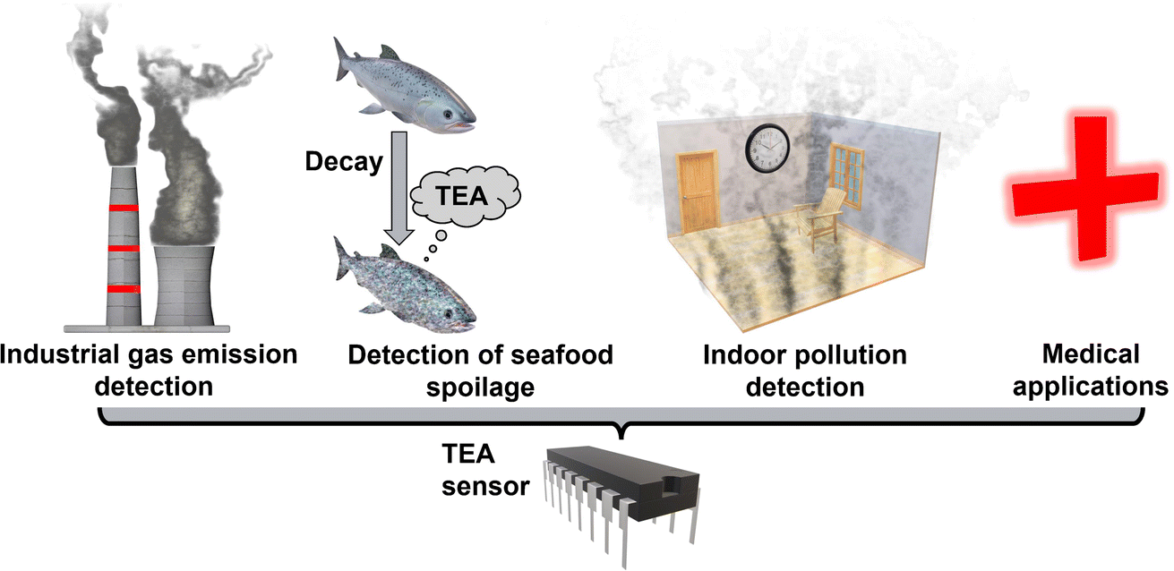 | ||
| Fig. 1 Application of TEA sensor. | ||
In the research of semiconductor TEA gas sensors, those based on different metal oxides have been widely studied, such as SnO2,5 In2O3,6 ZnO,7 CuO,8etc. Among them, In2O3 has been favored by researchers because of its good gas-sensing properties of TEA, however, there are still issues such as slow recovery time and high operating temperature.9 For In2O3-based TEA gas-sensing material, the current research mainly focuses on controlling the morphology of In2O3,10 doping with noble metals,11 forming heterojunctions with other oxides,12etc., wherein, the loading of Pd nanoparticles (NPs) is an effective method for modifying In2O3, where Pd NPs can influence the overall energy and catalytic activity, while also controlling the number of charge carriers (electrons and holes) in the suctor,13 lowering the activation energy of the system and promoting electron transfer,14–16 and ultimately improve the comprehensive gas sensing performance of In2O3.17–19 In addition to the catalytic effect of Pd NPs that can effectively improve the gas sensitivity of In2O3, PdO also plays an important role in improving the gas sensitivity of In2O3, PdO is a P-type semiconductor, it is easy to form a P–N heterojunction when combined with N-type semiconductor In2O3, which will increase the thickness of the electron depletion layer (EDL) of the material and form a carrier transport channel, which will help to provide more adsorption and reaction sites, and ultimately improve the gas sensing performance.20,21
For gas-sensing materials, the number of active sites and electron transport channels, and the electron transport efficiency have important impacts on the gas-sensing performance,20,22 so how to enhance the related properties has become a problem that researchers must face, and these properties can be improved through the preparation method of materials. Among the current common Pd species loading methods, the common ones are NaBH4 reduction method,17 ultraviolet light reduction method,23 one-pot method,24etc. These methods have their own advantages, and the Pd species loaded by these methods mainly play the role of surface modification or lattice doping, which promote the gas sensing performance by affecting the carrier distribution, reducing the reaction activation energy20 and increasing the active sites and electron transport channels. Although surface modification and lattice doping play a positive role, however, they cannot affect the specific surface area (SSA) and pore structure of the base material, which is closely related to the gas sensing performance. In addition, if the preparation time is too long, it is easy to occur the poisoning of precious metals, which is easy to lead to the reduction of the material's activity or even inactivation.20
In this study, Pd/PdO–In2O3 gas-sensing material were successfully prepared by a simple precursor-loaded Pd species and combined with a subsequent pyrolysis strategy, and exhibited excellent gas-sensing performance for TEA. Compared with NaBH4-reduced Pd–In2O3 gas-sensing material prepared in this study, Pd/PdO–In2O3 showed higher TEA sensitivity and faster response/recovery (res/rec) speed. Further analysis and characterization found that this unique precursor doping method causes Pd species to be oxidized to PdO during the pyrolysis process of the precursor, and due to the phase change and high temperature of the precursor, the Pd species distributed only on the surface of the precursor enters between the In2O3 nanoparticles and forms PdO, which not only forms a large number of P–N heterojunctions (PdO–In2O3) to accelerate electron transport, but also, PdO surrounded by In2O3 nanoparticles has the opportunity to form numerous electron transport channels and active sites to improve the gas sensing performance. At the same time, the stable property of PdO can effectively avoid the occurrence of noble metal poisoning and help to improve the long-term stability of the sensors. The current research ideas can further expand its scope of application and have reference significance for future related research.
Experimental section
As depicted in Fig. 2a, Pd species were loaded using two different methods (method 1: commonly used NaBH4 reduction method, method 2: precursor loading method). Fig. 2b shows a simple schematic diagram of the sensor and its performance testing device, the detailed schematics can be found in Fig. S1,† with detailed experimental details, analysis and the preparation process of the gas sensor can be obtained in the ESI.†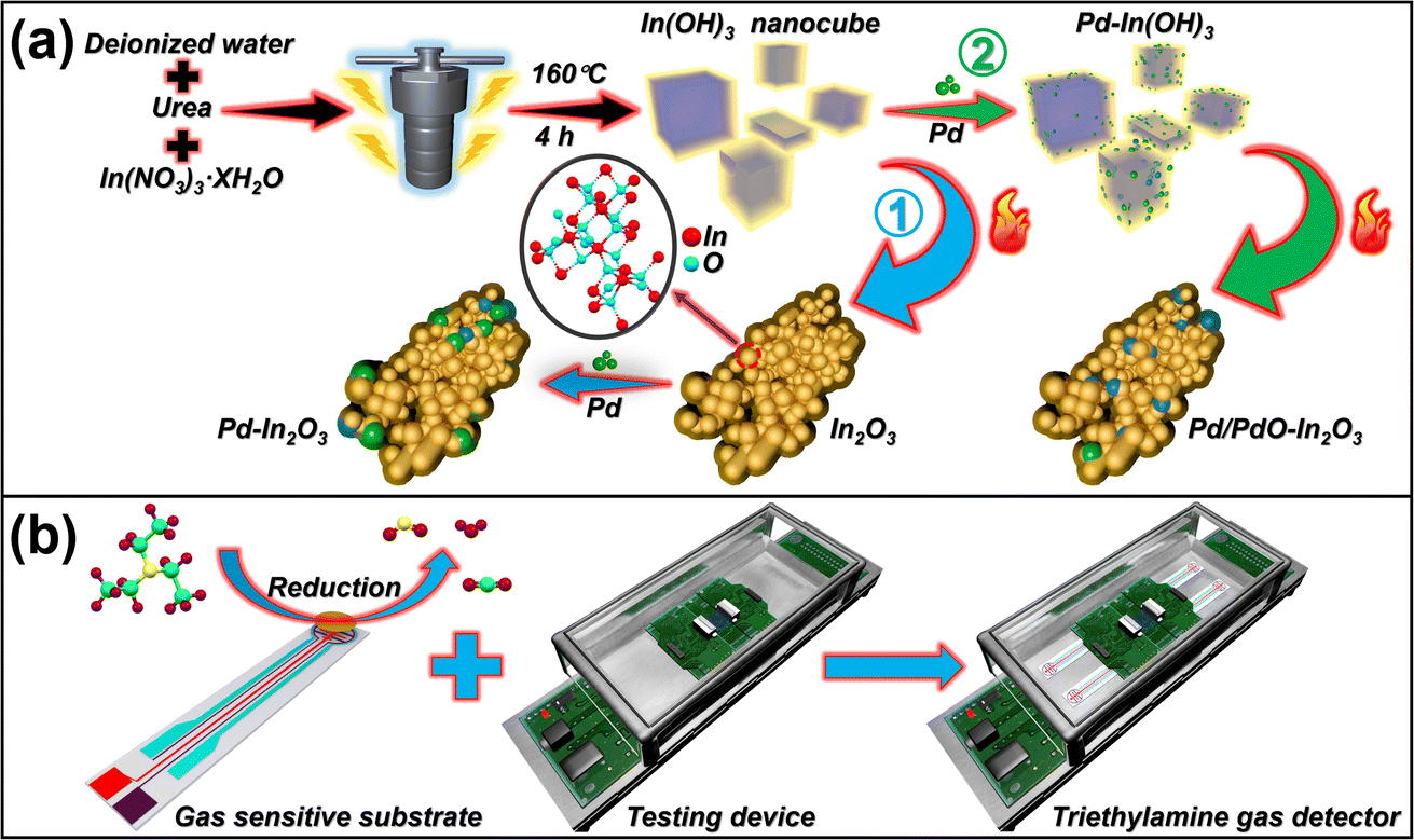 | ||
| Fig. 2 (a) Preparation process of Pd–In2O3 and Pd/PdO–In2O3, (b) sensor and performance testing device. | ||
Results and discussion
Structural and morphological characteristics
First, the phase structures of the corresponding samples were analyzed using X-ray diffraction (XRD). As illustrated in Fig. 3a, the as-prepared In(OH)3 exhibits a narrow and sharp diffraction peak that corresponds to the PDF standard card PDF#76-1463, indicating high crystallinity and large grain size, there is no noticeable impurity peak, suggesting that the sample has high purity. Upon calcination of the In(OH)3 precursor, the phase structure undergoes a change, and In(OH)3 is dehydrated into In2O3, from Fig. 3a, the four strongest peaks correspond to the PDF standard card PDF#71-2195 of In2O3, corresponding to the (222), (400), (440), (622) crystal planes, and also have narrow and sharp diffraction peaks, indicating that good crystallinity. At the same time, we analyzed the XRD patterns of Pd/PdO–In2O3 after loading Pd, it can be seen from Fig. 3b that the XRD curves of Pd/PdO–In2O3 with different loadings did not change significantly, which indicated that during the functionalization process, the phase of In2O3 is hardly affected.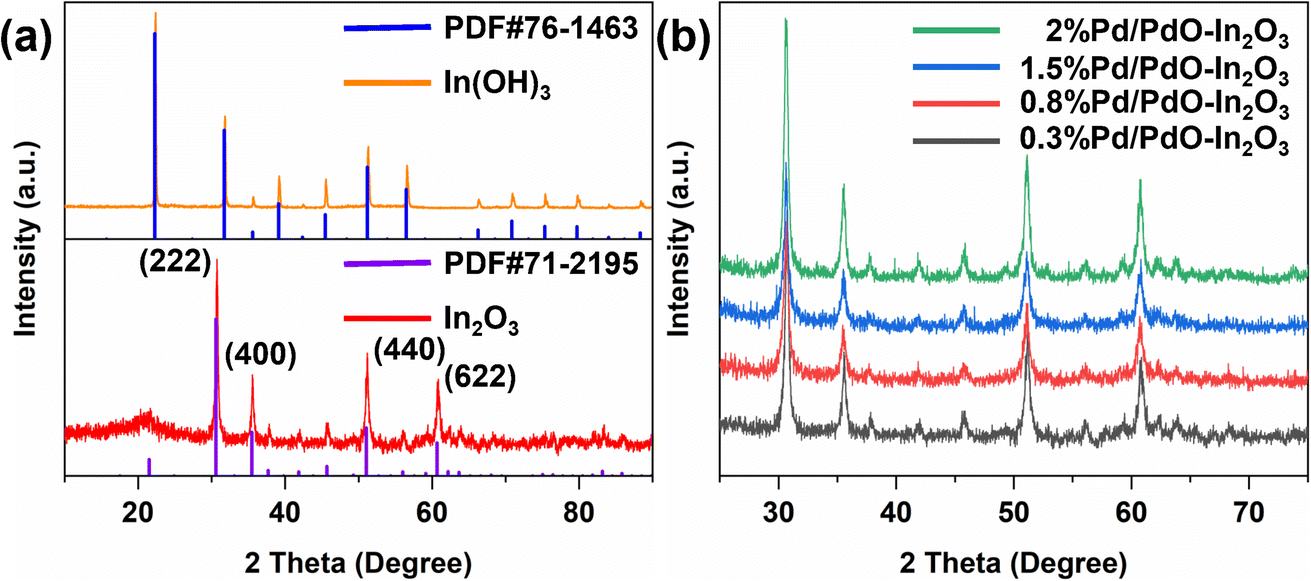 | ||
| Fig. 3 (a) XRD images of In(OH)3 and In2O3 and their PDF standard cards compared, (b) XRD contrast images of In2O3 with different Pd/PdO loadings. | ||
The morphology and structure of the samples were characterized. Fig. 4a is the scanning electron microscope (SEM) image of the In(OH)3 precursor, the SEM image shows that In(OH)3 exhibits a micro-nano cube structure, and the thermal gravimetric image of In(OH)3 (Fig. S2†) shows that In(OH)3 has no significant mass change after 350 °C, so we use 350 °C as the annealing temperature of the sample. Since In(OH)3 cubes are thermally decomposed into In2O3 and H2O, In(OH)3 nanocubes transform into In2O3 nanorods (Fig. 4b). The SEM images of Pd/PdO–In2O3 (Fig. 4c) shows no significant changes compared to In2O3, both exhibited a nanorod morphology at the microscopic level, this indicates that the modification of In2O3 by Pd/PdO did not cause major damage to its morphology, however, the uniformity of Pd/PdO–In2O3 was not as good as that of In2O3.
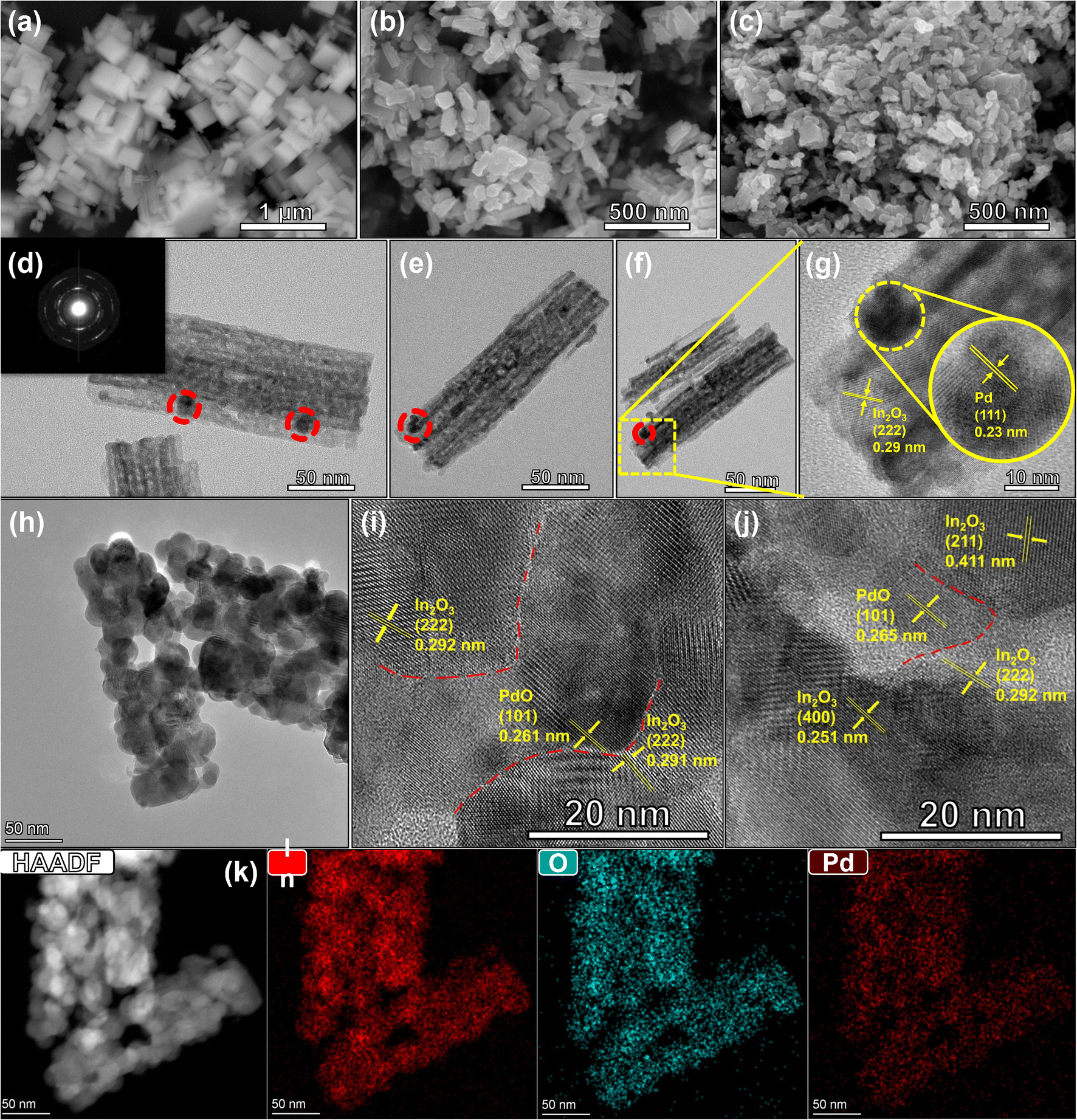 | ||
| Fig. 4 SEM images of (a) In(OH)3, (b) In2O3 nanorods, (c) 0.8% Pd/PdO–In2O3 nanorods, (d)–(f) TEM images of 0.8% Pd–In2O3, (g) HRTEM image of 0.8% Pd–In2O3, (h)–(j) HAADF-STEM images of 0.8% Pd/PdO–In2O3, (k) Mapping images of 0.8% Pd/PdO–In2O3. | ||
To analyze the differences between Pd–In2O3 and Pd/PdO–In2O3, we further analyzed the transmission electron microscope (TEM) images of the samples. First, we tested the TEM and high-resolution TEM (HRTEM) images of Pd–In2O3. Fig. 4d–f shows that Pd nanoparticles are almost all distributed on the surface of In2O3 nanorods (this can be predicted from the loading method of Pd nanoparticles, because Pd nanoparticles are directly reduced by NaBH4, so Pd nanoparticles are only distributed on the surface of In2O3 (ref. 17 and 25)), which mainly play a role in surface modification of In2O3 nanorods, the selected area electron diffraction (SAED) of 0.8% Pd–In2O3 showed obvious polycrystalline diffraction rings (Fig. 4d inset), indicating excellent crystallinity. For Pd/PdO–In2O3, due to the effect of annealing in air, most of the Pd species exist in the form of PdO. To observe the distribution of PdO in In2O3, we used high-angle annular dark-field STEM (HAADF-STEM) to characterize the samples, from Fig. 4h, it can be seen that there is almost no surface distribution of Pd nanoparticles, when the image is further enlarged, the presence of PdO can be observed (Fig. 4i and j), and PdO is surrounded by In2O3 nanoparticles, and an obvious multiple heterostructure is formed between PdO and In2O3 (shown by the red dotted line in Fig. 4i and j).
The SSA and pore size of the prepared samples were analyzed (Fig. 5a–c), the results showed a significant increase in the Brunauer–Emmett–Teller (BET) SSA of 0.8% Pd/PdO–In2O3 (Fig. 5c) compared to In2O3 (Fig. 5a) and 0.8% Pd–In2O3 (Fig. 5b) (67.58 m2 g−1 for 0.8% Pd/PdO–In2O3, compared to 48.75 m2 g−1 for In2O3 and 50.69 m2 g−1 for 0.8% Pd–In2O3). And the average pore size (APS) was significantly reduced (8.44 nm for 0.8% Pd/PdO–In2O3 (Fig. 5c inset), 13.40 nm for In2O3 (Fig. 5a inset), 13.09 nm for 0.8% Pd–In2O3 (Fig. 5b inset)). The increase of the SSA and the decrease of the pore size mean that the size/agglomeration of the In2O3 nanoparticles has changed, which indicates that the addition of PdO altered the size/agglomeration of In2O3 nanoparticles. In contrast, there was no significant difference in the BET SSA and APS between In2O3 and 0.8% Pd–In2O3, indicating that the surface modification of Pd nanoparticles had little effect on the BET SSA and pore size of In2O3.
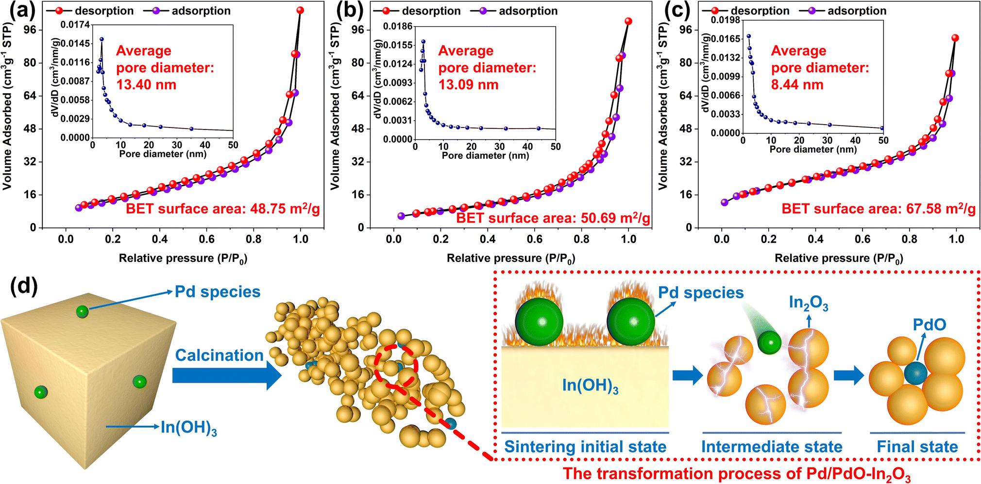 | ||
| Fig. 5 Nitrogen adsorption/desorption and pore size distribution curves: (a) In2O3 nanorods, (b) 0.8% Pd–In2O3 nanorods, (c) 0.8% Pd/PdO–In2O3 nanorods. (d) Formation mechanism of PdO–In2O3 heterojunction. | ||
In conclusion, the Pd species of Pd–In2O3 and Pd/PdO–In2O3 have obvious distribution differences, and the Pd nanoparticles in Pd–In2O3 are randomly distributed on the surface of In2O3 nanorods, which mainly play the role of surface modification for In2O3 nanorods. For Pd/PdO–In2O3, part of the PdO enters between the In2O3 nanoparticles, forming multiple heterojunction structures with the In2O3 nanoparticles, which indicates that under the dual effects of In(OH)3 phase transition and heat treatment, the Pd species is transformed into PdO, and the loading position changes, so that part of the Pd species that was only distributed on the surface of In(OH)3 before is transformed into PdO that enters the gap between In2O3 nanoparticles (Fig. 5d), this transformation not only changes the arrangement of In2O3 nanoparticles, which is conducive to the formation of more electron transport channels, but also facilitates the formation of p–n heterojunction between PdO and In2O3, thereby accelerating the transport of carrier.26,27
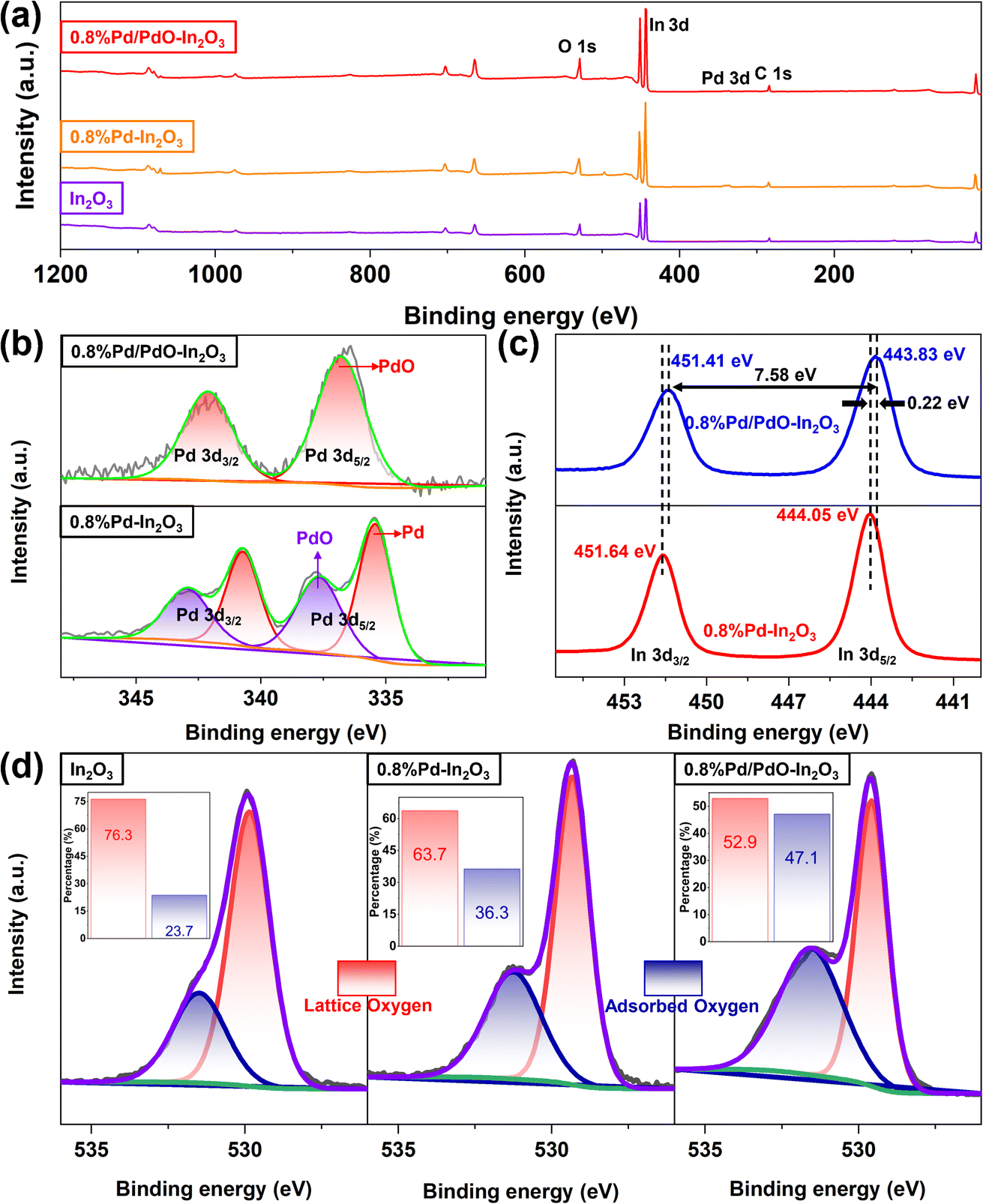
X-ray photoelectron spectroscopy (XPS) spectra of different samples were tested and all peaks were calibrated using the C 1s peak at 284.8 eV. Fig. 6a is the XPS full-spectrum image of different samples, no obvious impurity peaks were found in all samples, indicating that the samples were not contaminated by impurity elements during the preparation process. For 0.8% Pd/PdO–In2O3, its Pd 3d spectrum can be almost all assigned to PdO, which indicates that heat treatment and air oxidation almost convert most of the Pd to PdO (Fig. 6b). For 0.8% Pd–In2O3, the Pd 3d spectrum can be assigned to Pd and PdO (Fig. 6b), indicating that most of the Pd elements exist in the form of monovalent, which is consistent with the HRTEM image analysis results. For 0.8% Pd/PdO–In2O3, the electron spin coupling gap of In 3d is 7.58 eV (Fig. 6c), which indicates that the In element exists in the form of In2O3, notably, compared to 0.8% Pd–In2O3, the In 3d peak of 0.8% Pd/PdO–In2O3 shifted about 0.22 eV towards the low binding energy, this indicates an electron transfer from In2O3 to PdO.28 The O 1s spectra of In2O3, 0.8% Pd–In2O3, 0.8% Pd/PdO–In2O3 were compared (Fig. 6d), the results show that 0.8% Pd/PdO–In2O3 has a higher adsorbed oxygen content, which can provide more reactive species for the gas-sensing reaction,29,30 this is an important reason for the better gas-sensing performance of 0.8% Pd/PdO–In2O3.
 | ||
| Fig. 6 (a) XPS full spectrum image of different samples, XPS high-resolution images of (b) Pd 3d, (c) In 3d and (d) O 1s. | ||
The mass fraction of Pd element in several groups of samples was determined by inductively coupled plasma optical emission spectrometer (ICP-OES) (Table S1†) analysis, and the results showed that the Pd content in 0.8% Pd–In2O3 was higher than that in 0.8% Pd/PdO–In2O3, this may be due to phenomena such as solvent taking away part of the noble metal and thermal treatment losing noble metal in the process of material preparation, and the actual mass percentage of Pd in 0.8% Pd/PdO–In2O3 is 0.42%.
Gas-sensing performance
All gas sensitivity tests are carried out within the range of 30–50% RH (unless otherwise specified).Fig. 7a summarizes the relationship between the response values of different sensors and the operating temperature. It can be seen that the response value of 0.8% Pd/PdO–In2O3 reached the highest 1380 at 150 °C, and the response value of the Pd/PdO–In2O3 sensor is generally better than that of the Pd–In2O3 control group, and the response value of the Pd–In2O3 sensor has no obvious change compared with the response value of the In2O3 sensor, which means that the surface modification of Pd nanoparticles failed to effectively enhance the sensitivity of In2O3 to TEA, however, its recovery characteristics were improved (Fig. S3†). Fig. 7b shows that the res/rec time of the 0.8% Pd/PdO–In2O3 sensor is 30 s/90 s at a high response of 1380, showing a fast res/rec rate, this has a positive effect on the real-time detection of the sensor. The 0.8% Pd–In2O3 sensor has a response value of 215 to 10 ppm TEA at the optimal operating temperature and a res/rec time of 99 s/341 s (Fig. 7c), its response value and res/rec time are lower than 0.8% Pd/PdO–In2O3 sensor.
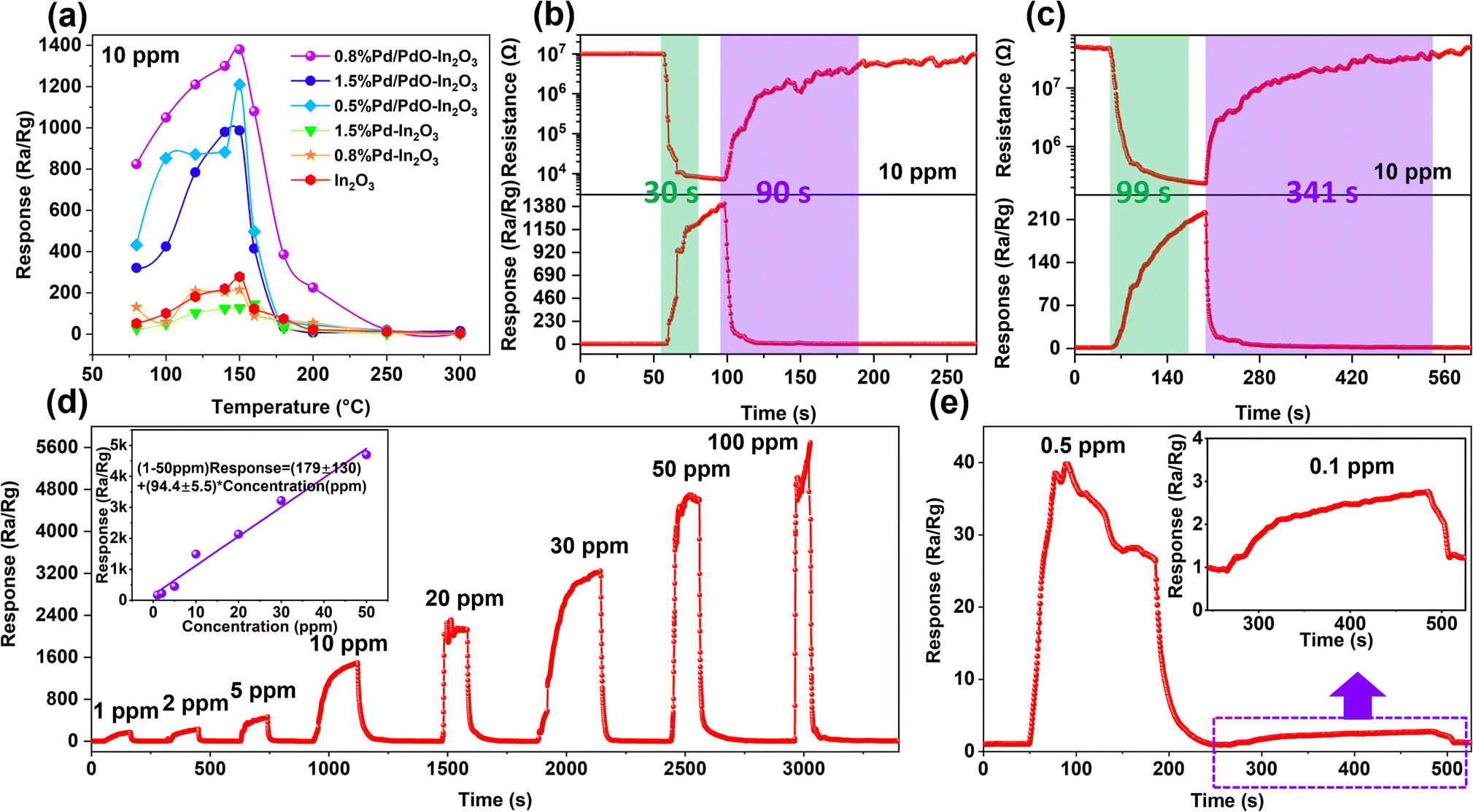 | ||
| Fig. 7 Relative humidity: 45%, (a) the relationship between response values and operating temperature of different sensors, (b) transient resistance curve and response-time curve of 0.8% Pd/PdO–In2O3 sensor, (c) transient resistance curve and response-time curve of 0.8% Pd–In2O3 sensor, (d) transient response curve of 0.8% Pd/PdO–In2O3 sensor to different TEA concentration (inset: linear fitting of sensor response values to 1–50 ppm TEA), (e) transient response curve of 0.8% Pd/PdO–In2O3 sensor to low concentration TEA. | ||
The response-time curves of the sensor to different concentrations of TEA were tested (Fig. 7d) to study the TEA concentration test range of the 0.8% Pd/PdO–In2O3 sensor, Fig. 7d shows that the sensor has a strong and rapid response to 1–100 ppm of TEA. When the TEA concentration increases to 100 ppm, the response value of the sensor does not increase significantly compared to 50 ppm. At the same time, we have performed a linear fitting on the response value of 1–50 ppm, it shows that the sensor has a good linear relationship of response value in the concentration range of 1–50 ppm TEA (Fig. 7d illustration). A low concentration of TEA was tested, and Fig. 7e shows that the sensor still has a certain response value to 0.1 ppm TEA, combined with Fig. 7d, it shows that the detection limit of the sensor is 0.1–100 ppm.
It can be observed from Fig. 8a that the response value of the 0.8% Pd/PdO–In2O3 sensor did not change significantly during the 11 consecutive cycle stability tests, the relative standard deviation (RSD) of its response value was 5.2%. Meanwhile, the changes in response/recovery time during 11 cycles were statistically analyzed (Fig. 8b), revealing that the response time remained relatively stable as the cycle number increased, while the recovery time showed an increasing trend, this may be related to the incomplete desorption of the material and the decrease in desorption pathways caused by the increase in TEA concentration in the air. The selectivity of different sensors was also tested (Fig. 8c), it can be seen that the 0.8% Pd/PdO–In2O3 sensor has no obvious response to other common gases except formaldehyde and ammonia, indicating that its selectivity is better, in contrast, the selectivity of 0.8% Pd–In2O3 and In2O3 sensors was also tested, it can be seen that the surface modification of In2O3 nanorods with Pd nanoparticles does not effectively improve its selectivity, both of them show relatively high sensitivity to TEA and ammonia.
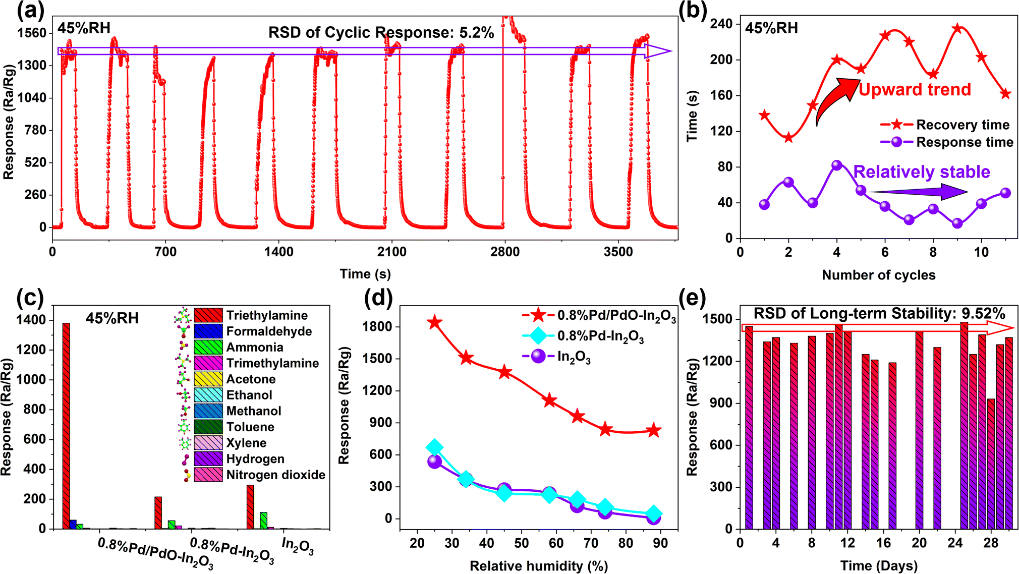 | ||
| Fig. 8 Test environment: (10 ppm, 150 °C). (a) 11-cycle stability of 0.8% Pd/PdO–In2O3 sensor. (b) Statistical analysis of response–recovery time variation trend in cycles. (c) Selective testing of different sensors. (d) Humidity resistance test. (e) Long-term stability of 0.8% Pd/PdO–In2O3 sensor. | ||
The moisture resistance test is shown in Fig. 8d, in contrast to the sharp decrease in the response value of the In2O3 and 0.8% Pd–In2O3 sensor after relative humidity (RH) augmentation, although the 0.8% Pd/PdO–In2O3 sensor also showed a decrease in response value, however, it still had a high response of 828 to 10 ppm TEA at 88% RH. The reason for the decrease in the response value is related to the fact that water molecules occupy the active sites of the material, excessive water molecules compete with the adsorption of oxygen molecules on the active sites of the material, which weakens the oxygen adsorption capacity of the material and causes the air resistance of the material to decrease,31 similarly, when the gas-sensing reaction is in progress, water molecules will also compete with TEA molecules for active sites, in summary, the competition between water molecules and oxygen molecules/TEA molecules reduces the response value of the sensor. Different from some research that uses highly conductive materials to resist the impact of humidity,32,33 in this study, the reason for the enhanced moisture resistance is related to the catalytic overflow effect of PdO, which increases the number of oxygen anions on the surface of In2O3,31 which helps reduce the impact of water molecules.
In terms of long-term stability, a random long-term stability test was carried out on the 0.8% Pd/PdO–In2O3 sensor within 30 days (Fig. 8e). The results showed that the response value of the sensor did not drop/rise significantly, the long-term stability of the sensor has a response value RSD of 9.52%, showing a certain degree of fluctuation. The reason of fluctuation is mainly related to the humidity of the test environment, the slight variation in gas concentration during each test and the stability of the test equipment, the stability of the sensor can be improved by methods such as further modification to enhance the material's humidity resistance, establishing a humidity control group to reduce the response value variation caused by humidity, reducing gas concentration variation caused by human factors, using testing instruments with stable output signals, etc. Finally, the gas-sensing performance of recent related works are listed and shown in Table S2,† it can be seen that the results from this work are superior.
Gas-sensing mechanism
It is well known that In2O3 and PdO are typical metal oxide semiconductor (MOS) materials, and the most intuitive manifestation of their sensing performance is the change of their resistance. Simply put, the gas sensing process is the process of interaction between the sensing material and the target gas, this process will produce a series of chemical and physical changes, fully understanding this series of changes is of positive significance for the development of high-performance gas sensors. In the current study, the gas-sensing mechanism of MOS is usually explained using the adsorbed oxygen model and the EDL theory. In this study, when the gas-sensing reaction has not yet started, Pd/PdO–In2O3 exposed to the air will adsorb oxygen in the air, and consume electrons in its own conduction band to convert the adsorbed oxygen molecules into oxyanions (Fig. 9a and b), since in this study, the optimal operating temperature of the sensor is 150 °C, the oxyanion species at this time may be O2−/O−,34,35 the oxygen adsorption process increases the thickness of the EDL of Pd/PdO–In2O3, so the sensor at this time exhibits high resistance. When Pd/PdO–In2O3 is exposed to TEA molecules (Fig. 9c), the adsorbed oxygen anions react with TEA molecules and return electrons to Pd/PdO–In2O3, resulting in thinning of the EDL of Pd/PdO–In2O3, this in turn reduces the resistance of the sensor. The process described above can be described by the following equation:| O2(g) → O2(ads) |
| O2(ads) + e− → O2−(ads)/O2(ads) + 2e− → 2O−(ads) |
| C6H15N + O2−/O− → CO2 + H2O + NO2 |
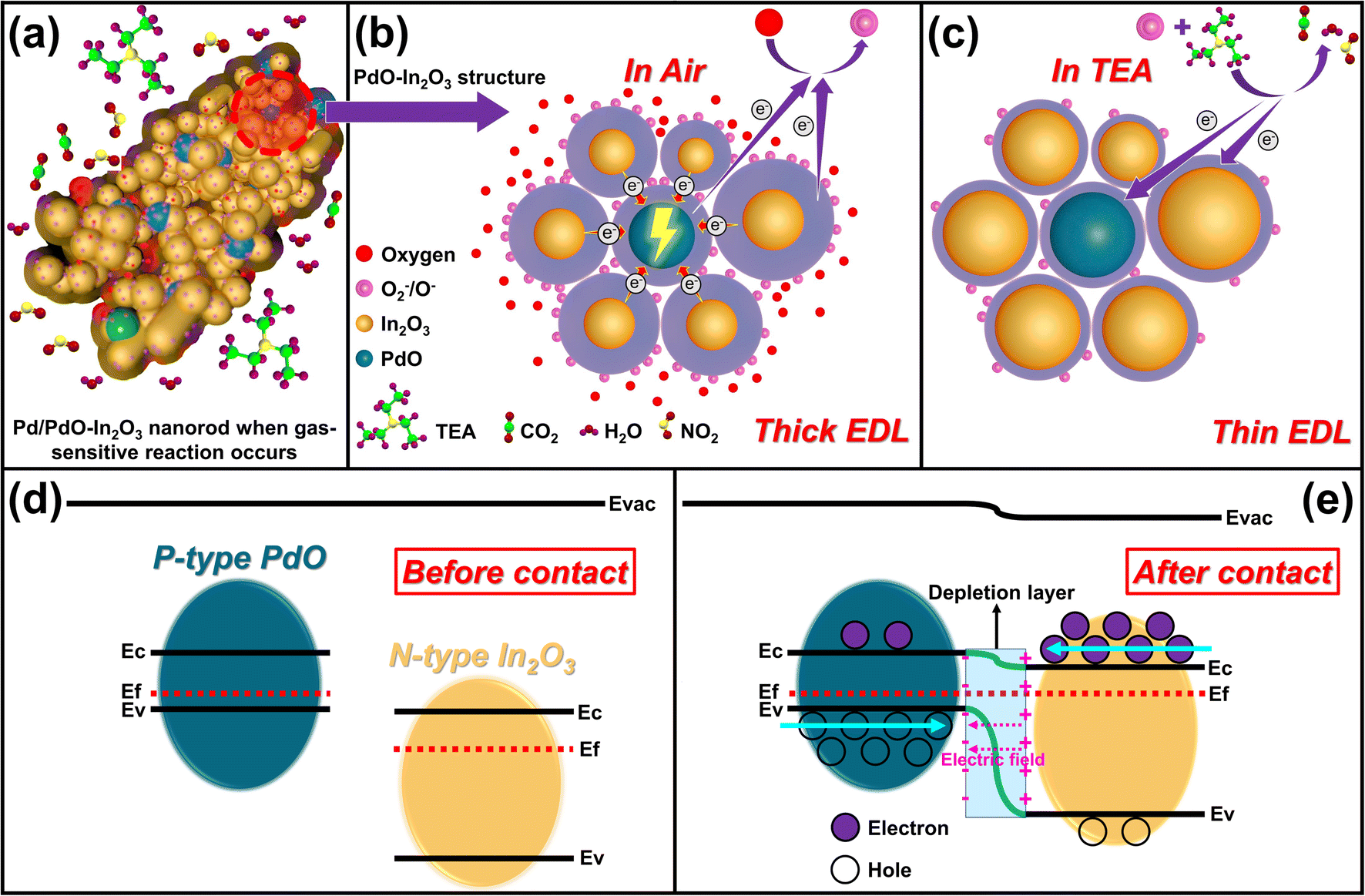 | ||
| Fig. 9 (a) Schematic diagram of Pd/PdO–In2O3 during gas sensing reaction. Schematic diagram of gas sensing mechanism: (b) EDL in air, (c) EDL in TEA, (d) band structure of PdO and In2O3 before contact, (e) band structure of PdO and In2O3 after contact. | ||
In this study, due to the introduction of Pd species, the gas sensing performance of Pd/PdO–In2O3 was significantly improved compared with the pristine In2O3 sensor, and the improvement of Pd/PdO–In2O3 sensing performance was mainly due to the unique distribution of Pd species, electronic sensitization, and chemical sensitization are related.
As mentioned earlier, compared with Pd–In2O3, the Pd species in Pd/PdO–In2O3 partly entered between In2O3 nanoparticles and mainly existed in the form of PdO. Different from the surface modification effect of Pd nanoparticles distributed only on the surface of In2O3, this unique distribution enables the formation of multiple heterostructures between PdO and In2O3 nanoparticles, this structure leads to an increase in the rate of electron transport and the number of electron transport channels in the material (Fig. 9b). At the same time, the unique distribution of PdO changes the distribution/accumulation of In2O3 nanoparticles, which significantly increases the SSA of the material, which is conducive to the attachment of more gases and participates in the gas-sensing reaction process, thus improving the gas-sensing performance.
Specifically, in terms of electronic sensitization, first of all, since PdO is a p-type semiconductor36 and In2O3 is an n-type semiconductor, a typical p–n heterojunction will be formed between them. Since the work function of PdO is higher than that of In2O3 (ref. 37 and 38) (Fig. 9d), the electrons in the conduction band of In2O3 will transfer to the work function of PdO, while the holes in the valence band of PdO will transfer to In2O3, which will eventually lead to the Fermi level balance of the two semiconductors,39 due to the transfer of electrons, a wider EDL will be formed, and the energy band bending will occur at the contact interface between PdO and In2O3 (Fig. 9e), and finally the air resistance (Ra) of the material will increase significantly (Fig. S4†), since PdO exists as a small amount of modifier, Pd/PdO–In2O3 behaves as an n-type semiconductor, so its response value is defined as Ra/Rg (Rg = gas resistance), electron sensitization mainly plays a role in increasing Ra.
Specifically, in terms of chemical sensitization, compared with pure In2O3 nanorods, the heterojunction between PdO and In2O3 forms a wider EDL, this is mainly the catalyst role of PdO to promote the transformation of oxygen molecules into O atoms (O2(gas) ↔ 2O(ads)), the increased oxygen atoms will partially spill over to the surface of In2O3, thus capturing electrons in the conduction band of In2O3 to form oxygen anions, which ultimately leads to an increase in the amount of oxygen adsorbed by Pd/PdO–In2O3. Increased oxyanions mean that more oxygen species can be provided for the gas-sensing reaction, increasing the probability of TEA molecules interacting with oxyanions. Therefore, the chemosensitization effect accelerates the sensing reaction and improves the sensing performance.
Conclusions
In conclusion, we successfully prepared Pd/PdO–In2O3 nanorods with unique PdO distribution by precursor loading of Pd species and combined with subsequent calcination strategy. Which shows excellent sensing performance for TEA. The 0.8% Pd/PdO–In2O3 sensor exhibited a high response of 1380 and a fast res/rec time of 30 s/90 s for 10 ppm TEA, and with good selectivity and stability at an optimal operating temperature of 150 °C, and a detection limit below 0.1 ppm. The gas sensing enhancement mechanism of PdO with unique distribution was further studied, the results show that the multiple heterojunctions formed between PdO particles and In2O3 provide more electron transport channels and accelerate electron transport, this is the main reason why the 0.8% Pd/PdO–In2O3 sensor has high response and fast res/rec characteristics. The Pd/PdO–In2O3 sensor has a good application prospect in TEA detection because of its good sensing performance.Conflicts of interest
There are no conflicts to declare.Acknowledgements
This work was funded by the National Key Research and Development Program of China (2022YFB3803600), the Key Research and Development Program of Yunnan Province (202302AF080002), Yunnan Yunling Scholars Project, Yunnan basic applied research project (202101AT070013), Young and middle-aged academic and technical leaders reserve talent project in Yunnan Province (202005AC160015). Authors thank the Electron Microscopy Center, the Advanced Computing Center, the Advanced Analysis and Measurement Center of Yunnan University for the sample testing and computations service.Notes and references
- L. L. Guo, B. Zhang, X. L. Yang, S. S. Zhang, Y. Wang, G. D. Wang and Z. Y. Zhang, Sens. Actuators, B, 2021, 343, 130126 CrossRef CAS.
- C. H. Hu, L. M. Yu, S. L. Li, M. L. Yin, H. B. Du and H. F. Li, Sens. Actuators, B, 2022, 355, 131246 CrossRef CAS.
- B. Akesson, I. Floren and S. Skerfving, Br. J. Ind. Med., 1985, 42, 848–850 Search PubMed.
- B. Gandu, K. Sandhya, A. G. Rao and Y. V. Swamy, Bioresour. Technol., 2013, 139, 155–160 CrossRef CAS PubMed.
- Y. H. Zou, S. Chen, J. Sun, J. Q. Liu, Y. K. Che, X. H. Liu, J. Zhang and D. J. Yang, ACS Sens., 2017, 2, 897–902 CrossRef CAS PubMed.
- S. X. Shi, F. Zhang, H. M. Lin, Q. Wang, E. B. Shi and F. Y. Qu, Sens. Actuators, B, 2018, 262, 739–749 CrossRef CAS.
- W. R. Li, H. Y. Xu, T. Zhai, H. Q. Yu, Q. Xu, X. P. Song, J. Q. Wang and B. Q. Cao, J. Alloys Compd., 2017, 695, 2930–2936 CrossRef CAS.
- Y. P. Wu, W. Zhou, W. W. Dong, J. Zhao, X. Q. Qiao, D. F. Hou, D. S. Li, Q. C. Zhang and P. Y. Feng, Cryst. Growth Des., 2017, 17, 2158–2165 CrossRef CAS.
- J. J. Liu, L. Y. Zhang, J. J. Fan and J. G. Yu, Small, 2022, 18, 2104984 CrossRef CAS PubMed.
- W. Yang, L. Feng, S. H. He, L. Y. Liu and S. T. Liu, ACS Appl. Mater. Interfaces, 2018, 10, 27131–27140 CrossRef CAS PubMed.
- L. L. Zheng, T. T. Ma, Y. Q. Zhao, Y. S. Xu, L. Sun, J. Zhang and X. H. Liu, Sens. Actuators, B, 2019, 290, 155–162 CrossRef CAS.
- Q. Ma, S. S. Chu, H. Li, J. Guo, Q. Zhang and Z. Q. Lin, Appl. Surf. Sci., 2021, 569, 151074 CrossRef CAS.
- V. Subramanian, E. E. Wolf and P. V. Kamat, J. Am. Chem. Soc., 2004, 126, 4943–4950 CrossRef CAS PubMed.
- Y. Guo, B. H. Liu, Z. H. Duan, Z. Yuan, Y. D. Jiang and H. L. Tai, Mater. Chem. Phys., 2023, 302, 127768 CrossRef CAS.
- T. Tang, Z. Li, Y. F. Cheng, H. G. Xie, X. X. Wang, Y. L. Chen, L. Cheng, Y. Liang, X. Y. Hu, C. M. Hung, N. D. Hoa, H. Yu, B. Y. Zhang, K. Xu and J. Z. Ou, J. Hazard. Mater., 2023, 451, 131184 CrossRef CAS PubMed.
- X. Duan, Z. Duan, Y. Zhang, B. Liu, X. Li, Q. Zhao, Z. Yuan, Y. Jiang and H. Tai, Sens. Actuators, B, 2022, 369, 132302 CrossRef CAS.
- X. J. Liu, K. R. Zhao, X. L. Sun, C. Zhang, X. P. Duan, P. Y. Hou, G. Zhao, S. W. Zhang, H. C. Yang, R. Y. Cao and X. J. Xu, Sens. Actuators, B, 2019, 285, 1–10 CrossRef CAS.
- Y. Wang, H. S. Zhang and J. L. Cao, Mater. Chem. Phys., 2022, 279, 124749 Search PubMed.
- J. H. Lee, J. H. Kim, J. Y. Kim, A. Mirzaei, H. W. Kim and S. S. Kim, Sensors, 2019, 19, 4276 CrossRef CAS PubMed.
- H. C. Ji, W. Zeng and Y. Q. Li, Nanoscale, 2019, 11, 22664–22684 RSC.
- Y. B. Luo, B. X. An, J. L. Bai, Y. R. Wang, X. Cheng, Q. Wang, J. P. Li, Y. F. Yang, Z. K. Wu and E. Q. Xie, J. Colloid Interface Sci., 2021, 599, 533–542 CrossRef CAS PubMed.
- R. Ahmad, S. M. Majhi, X. X. Zhang, T. M. Swager and K. N. Salama, Adv. Colloid Interface Sci., 2019, 270, 1–27 CrossRef CAS PubMed.
- F. B. Gu, M. Y. Di, D. M. Han, S. Hong and Z. H. Wang, ACS Sens., 2020, 5, 2611–2619 CrossRef CAS PubMed.
- P. Rai, J. W. Yoon, C. H. Kwak and J. H. Lee, J. Mater. Chem. A, 2016, 4, 264–269 RSC.
- H. Y. Lai and C. H. Chen, J. Mater. Chem., 2012, 22, 13204–13208 RSC.
- X. X. Chang, T. Wang, P. Zhang, J. J. Zhang, A. Li and J. L. Gong, J. Am. Chem. Soc., 2015, 137, 8356–8359 CrossRef CAS PubMed.
- Z. J. Li, H. Li, Z. L. Wu, M. K. Wang, J. T. Luo, H. D. Torun, P. A. Hu, C. Yang, M. Grundmann, X. T. Liu and Y. Q. Fu, Mater. Horiz., 2019, 6, 470–506 RSC.
- K. Zhang, S. W. Qin, P. G. Tang, Y. J. Feng and D. Q. Li, J. Hazard. Mater., 2020, 391, 122191 CrossRef CAS PubMed.
- Z. M. Deng, Y. M. Zhang, D. Xu, B. Y. Zi, J. Y. Zeng, Q. Lu, K. Xiong, J. Zhang, J. H. Zhao and Q. J. Liu, ACS Sens., 2022, 7, 2577–2588 CrossRef CAS PubMed.
- J. M. Walker, S. A. Akbar and P. A. Morris, Sens. Actuators, B, 2019, 286, 624–640 CrossRef CAS.
- J. J. Liu, L. Y. Zhang, J. J. Fan, B. C. Zhu and J. G. Yu, Sens. Actuators, B, 2021, 331, 129425 CrossRef CAS.
- Z. Yuan, Q. N. Zhao, Z. H. Duan, C. Y. Xie, X. H. Duan, S. R. Li, Z. B. Ye, Y. D. Jiang and H. L. Tai, Sens. Actuators, B, 2022, 363, 131790 CrossRef CAS.
- T. Tang, Z. Li, Y. F. Cheng, K. Xu, H. G. Xie, X. X. Wang, X. Y. Hu, H. Yu, B. Y. Zhang, X. W. Tao, C. M. Hung, N. D. Hoa, G. Y. Chen, Y. X. Li and J. Z. Ou, J. Mater. Chem., 2023, 11, 6361–6374 RSC.
- S. M. Majhi, H. J. Lee, H. N. Choi, H. Y. Cho, J. S. Kim, C. R. Lee and Y. T. Yu, Crystengcomm, 2019, 21, 5084–5094 RSC.
- N. Barsan and U. Weimar, J. Electroceram., 2001, 7, 143–167 CrossRef CAS.
- S. R. Wang, Y. J. Wang, J. Q. Jiang, R. Liu, M. Y. Li, Y. M. Wang, Y. Su, B. L. Zhu, S. M. Zhang, W. P. Huang and S. H. Wu, Catal. Commun., 2009, 10, 640–644 CrossRef CAS.
- Q. Li, W. Liang and J. K. Shang, Appl. Phys. Lett., 2007, 90, 063109 CrossRef.
- M. H. Dun, M. H. Tang, D. Y. Zhao, X. H. Li and X. T. Huang, Sens. Actuators, B, 2022, 358, 131520 CrossRef CAS.
- Y. Liu, S. T. Yao, Q. Y. Yang, P. Sun, Y. Gao, X. S. Liang, F. M. Liu and G. Y. Lu, RSC Adv., 2015, 5, 52252–52258 RSC.
Footnote |
| † Electronic supplementary information (ESI) available. See DOI: https://doi.org/10.1039/d3ta02405a |
| This journal is © The Royal Society of Chemistry 2023 |