
“Twisted” small molecule donors with enhanced intermolecular interactions in the condensed phase towards efficient and thick-film all-small-molecule organic solar cells†
Xiafei
Cheng
ac,
Ziqi
Liang
a,
Shifeng
Liang
a,
Xuwen
Zhang
a,
Jie
Xu
a,
Yan
Xu
a,
Wang
Ni
*b,
Miaomiao
Li
 *a and
Yanhou
Geng
ad
*a and
Yanhou
Geng
ad
aSchool of Materials Science and Engineering, Tianjin Key Laboratory of Molecular Optoelectronic Science, Tianjin University, Tianjin, 300072, China. E-mail: miaomiao.li@tju.edu.cn
bScience and Technology on Power Sources Laboratory, Tianjin Institute of Power Sources, Tianjin, 300384, China. E-mail: niwang@tju.edu.cn
cSinopec (Beijing) Research Institute of Chemical Industry Co., Ltd., Beijing, 100013, China
dJoint School of National University of Singapore and Tianjin University, International Campus of Tianjin University, Binhai New City, Fuzhou 350207, China
First published on 29th May 2023
Abstract
How to achieve high crystallinity and suitable phase scale simultaneously from the perspective of molecular engineering remains a long-standing challenge for all-small-molecule organic solar cells (ASM-OSCs). Herein, two small molecule donors, named DRTT-2Se (with two alkylselenophenyl chains) and DRTT-6Se (with six alkylselenophenyl chains), were designed and synthesized by introducing “twisted” backbones and building units with strong intermolecular interactions. The “twisted” skeletons of the molecules can suppress the molecular crystallization and avoid excessive aggregation during the film forming process, while the strong intermolecular interactions of the building units can encourage the formation of ordered molecular packing and nanoscale phase separation via post-treatments. Owing to the enhanced intermolecular interactions induced by alkylselenophenyl side chains, DRTT-2Se and DRTT-6Se with a “twisted” structure displayed more ordered π–π packing, and retained the similar nanoscale microstructures in the blend films in comparison to the “twisted” molecule with alkylthiophenyl side chains (DRTT-T), yielding improved hole transport and reduced charge recombination in OSCs. In addition, the alkylselenophenyl substituted molecules showed higher HOMO energy levels, which caused the larger HOMO offset to drive exciton dissociation, but did not increase the energy loss. As a result, the ASM-OSCs based on the selenophene-containing donors exhibited higher FF and Jsc, and similar Voc, yielding superior PCEs (14.79% and 15.03%) compared to the DRTT-T based device (13.37%). More importantly, the appropriate film morphology made the device efficiency of DRTT-2Se and DRTT-6Se less sensitive to the thickness of active layers. This study provides some implications in designing small molecule donors with suitable crystallization behavior towards high-performance ASM-OSCs.
 Miaomiao Li | Miaomiao Li is an associate professor at the School of Materials Science and Engineering, Tianjin University, China. She received her B.S. degree from Lanzhou University in 2011, and PhD degree from Nankai University in 2016 under the supervision of Prof. Yongsheng Chen. From 2018 to 2019, she worked as a visiting scholar in Prof. René A. J. Janssen's group at Eindhoven University of Technology, the Netherlands. Her current research focuses on the molecular design and morphology control of low-cost organic photovoltaic materials. |
1. Introduction
Organic solar cells (OSCs) have drawn wide attention attributed to their unique merits of light-weight, multiple colors and great potential flexible and large-area solar cell panels through low-cost coating methods.1–3 Compared to polymer semiconductors, small molecule semiconductors show promising superiorities such as well-defined chemical molecular structures, easy purification and negligible batch-to-batch variation,4–7 making all-small-molecule OSCs (ASM-OSCs) have great potential in commercial applications. Through long-term efforts on molecular design and device optimization, ASM-OSCs have made great progress in recent years. However, most ASM-OSCs show power conversion efficiencies (PCEs) below 15%, which significantly lag behind those of OSCs based on polymer donors.8–15 In addition, the device efficiency of ASM-OSCs is often more sensitive to the thickness of the active layers than that of OSCs containing polymer components. The inferior PCE and the high sensitivity of the device performance to film thickness for ASM-OSCs are mainly derived from the unideal film morphology.16,17Generally, the appropriate film morphology is more difficult to be acquired for the ASM blend systems in comparison to the blends containing polymer components. The long molecular skeleton of polymer donors can facilitate the direct formation of bright interpenetrating film morphology. Nevertheless, for the ASM blend systems, small molecule donors and small molecule acceptors with relatively weak molecular interactions and limited conjugate length often present high configurational entropy of mixing, and tend to form finely intermixed donor/acceptor domains and homogeneous film morphology without distinct phase separation.18–21 Improving the crystallinity of the small molecule donors by enhancing molecular rigidity and planarity can allow the ASM blends to form phase-separated morphology.22–26 However, because of the easier molecular motion of the small molecules, the small molecules with high crystallinity are likely to form large crystals and to undergo excessive aggregation, leading to over-sized phase separation.22,26 This suggests that the suitable crystallization behavior of the molecules is the premise for the formation of ideal morphology with nanoscale network structures and meanwhile ordered molecular packing in ASM blend films. Besides, different from the polymer semiconductors in which charge carriers can transport through both interchain and intrachain channels, charge transport in small molecules is more dependent on intermolecular interactions, and hence it is more necessary for small molecules to form ordered stacking to guarantee efficient charge transport.20,27–31 Therefore, the crystallinity and intermolecular interactions of the small molecules play a vital role in determining the film microstructure and device performance for the ASM blend systems. To advance the performance of ASM-OSCs, the main challenge is focused on achieving desirable film morphology by molecular engineering in combination with post-treatments, adjustment of processing solvents and introduction of a third component.
Our group proposed a new molecular design strategy (schematically illustrated in Fig. 1a): twisting the conjugated backbones to slow down the crystallization rate of the molecules in the film forming process, and meanwhile promoting planarization of the molecular skeleton in the film state by introducing strong intermolecular interactions.32 The resulting donor molecules adopt twisted backbones in solution but planar geometry in the film state. The bulky side chains (alkyl or aryl chains) on the β-positions of the central thieno[3,2-b]thiophene (TT) units endow the molecules with “twisted” backbones, while the rotation barrier of twisting the inter-ring C–C linkage can be overcome in the condensed phase by the strong intermolecular interactions derived from the rigid and planar benzodithiophene (BDT) π bridges and 3-ethylrhodanine termini as well as the aromatic side chains on BDT or TT units. Owing to the slow self-assembly rate of the donor molecules with “twisted” backbones, the as-cast ASM blend films present relatively low crystallinity, and the molecular ordering and phase-separated morphology can be precisely tuned by post-annealing treatments. Moreover, the selection of the optimal thermal annealing (TA) conditions for the ASM-OSCs can be assisted by evaluating the crystallization parameters of these small molecule donors and nonfullerene acceptor in neat and blend films, which can reduce trial-and-error efforts on device optimization.19 Compared to the small molecule donor with alkyl side chains on the central TT unit, the molecule DRTT-T with alkylthiophenyl side chains on TT delivered superior performance with a PCE of ∼13%19 (Fig. 1b), which was related to the stronger molecular interactions in the film state coming from the alkylthiophenyl side chains.33–36 These results suggest that this molecular design strategy is promising to achieve high-efficiency ASM-OSCs.
 | ||
| Fig. 1 (a) Design strategy of the small molecule donors in this work. (b) Chemical structures of DRTT-T, DRTT-2Se, DRTT-6Se and N3. (c) The synthetic route to DRTT-2Se and DRTT-6Se. Reagents and conditions: (i) Pd(PPh3)4, toluene, microwave, 150 °C; (ii) 3-ethyl-2-thioxothiazolidin-4-one, triethylamine, CHCl3, reflux. (d and e) Absorption spectra of the small molecule donors in thin films without any post-treatments (d) and with TA treatment (e). (f) Illustrated diagram of the energy levels of the donor materials and N3. | ||
According to the above studies, we infer that further enhancement of the intermolecular interactions by side chain engineering should be an effective method to advance the photovoltaic performance of this type of “twisted” small molecule donors. Compared to sulfur, selenium is more polarizable, and has a larger atomic radius, lower electronegativity and stronger interatomic interactions. Replacement of the alkylthiophenyl chains with the alkylselenophenyl chains in the “twisted” small molecules should be able to further promote the intermolecular interactions through the π–π stacking by overlapping the large π orbital of the selenium atom.37–41 Therefore, in this work, we designed and synthesized two small molecule donors named DRTT-2Se and DRTT-6Se (Fig. 1b), by replacing the alkylthiophenyl chains with alkylselenophenyl chains on the TT or/and BDT unit in the molecule DRTT-T. Similar to DRTT-T, the two molecules with alkylselenophenyl side chains also possess twisted backbones, as revealed by the density functional theory (DFT) calculations (Fig. S1†). Nevertheless, DRTT-2Se and DRTT-6Se displayed increased intermolecular interactions and more ordered π–π packing, in comparison to DRTT-T. When blended with the nonfullerene acceptor N3 (ref. 42) (Fig. 1b), both small molecule donors with alkylselenophenyl side chains exhibited superior PCEs (14.79% for DRTT-2Se, 15.03% for DRTT-6Se) with higher fill factors (FFs) and short-circuit current densities (Jscs) owing to the efficient charge generation and transport with weak charge recombination and low energy disorder. Moreover, the photovoltaic performances of DRTT-2Se:N3 and DRTT-6Se:N3 based devices were less sensitive to the thickness of the active layers, showing great potential in practical applications.
2. Results and discussion
2.1. Material synthesis, photophysical and electrochemical properties
The synthetic route to DRTT-2Se and DRTT-6Se is shown in Fig. 1c. Microwave-assisted Stille coupling of compound 1 with 2 and 3 afforded compounds 4 and 5 in yields of 92% and 84%, respectively. Subsequent Knoevenagel condensations afforded DRTT-2Se and DRTT-6Se in yields over 80%. The synthetic details are depicted in the ESI.† The chemical structures of DRTT-2Se and DRTT-6Se were verified by NMR spectra (Fig. S2–S5†), matrix-assisted laser desorption ionization time-of-flight (MALDI-TOF) mass spectra (Fig. S6 and S7†) and elemental analyses.To evaluate the influence of the alkylselenophenyl side chains on optical absorption, the solution and film UV-vis-NIR absorption spectra of the molecules were characterized as illustrated in Fig. S8,†1d and e, and the relevant data are summarized in Table 1. In solution, the three molecules exhibited featureless absorption spectra with similar maximum absorption wavelengths (λsmax) at 532, 532 and 531 nm for DRTT-T, DRTT-2Se and DRTT-6Se, respectively. From solution to films, all the three molecules showed red-shifted and broadened absorption spectra with weak vibronic absorption, induced by the intermolecular interactions in the condensed phase. After TA at 90 °C, film absorption spectra featuring well-defined vibronic absorption peaks were observed for all the molecules, implying the formation of ordered microstructures in which the molecules adopted a planar geometry. Compared to the annealed DRTT-T film with the absorption maximum (λfilmmax) at 561/610 nm, the annealed DRTT-2Se and DRTT-6Se films showed red-shifted absorption peaks at 569/621 nm and 569/619 nm, respectively. The optical bandgaps (Eoptg) of these molecules calculated from the absorption onset of the thermally annealed films were 1.90, 1.86 and 1.86 eV for DRTT-T, DRTT-2Se and DRTT-6Se, respectively. The more redshifted absorption and narrower band gaps of DRTT-2Se and DRTT-6Se films indicate stronger intermolecular interactions in the solid state in comparison to DRTT-T. Electrochemical cyclic voltammetry (CV) was employed to estimate the highest occupied molecular orbital (HOMO) and the lowest unoccupied molecular orbital (LUMO) energy levels of the molecules in films. As shown in Fig. 1f, S9† and Table 1, the HOMO and LUMO energy levels were −5.57 eV/−3.36 eV, −5.51 eV/−3.46 eV and −5.54 eV/−3.44 eV for DRTT-T, DRTT-2Se and DRTT-6Se, respectively. Apparently, replacement of alkylthiophenyl side chains with alkylselenophenyl side chains caused slight upshifted HOMO and downshifted LUMO, which is consistent with the results of DFT calculations (as shown in Fig. S10†). This means that the HOMO offsets between the alkylselenophenyl substituted molecule donors and acceptor N3 are larger than that between DRTT-T and N3, which could provide a larger driving force for exciton dissociation at the donor:acceptor interfaces. However, because the offsets between the LUMO of N3 and the HOMO of the alkylselenophenyl substituted molecules are smaller than that between N3 and DRTT-T, the open-circuit voltage (Voc) of DRTT-2Se:N3 and DRTT-6Se:N3 based devices might decrease.
| Molecule | λ solmax [nm] | λ filmmax [nm] | λ film,TAmax [nm] | E optg [eV] | E LUMO [eV] | E HOMO [eV] |
|---|---|---|---|---|---|---|
| a The absorption maximum of the as-cast films. b The absorption maximum of the films with TA treatment. c The optical bandgap Eoptg was calculated from the absorption onset of the TA-treated film. d The LUMO and HOMO energy levels were calculated according to ELUMO = −(4.80 + Ereonset) eV and EHOMO = −(4.80 + Eoxonset) eV, in which Ereonset and Eoxonset represent reduction and oxidation onset potentials, respectively, versus the half potential of Fc/Fc+. | ||||||
| DRTT-T | 532 | 555, 588 | 561, 610 | 1.90 | −3.36 | −5.57 |
| DRTT-2Se | 532 | 555, 598 | 569, 621 | 1.86 | −3.46 | −5.51 |
| DRTT-6Se | 531 | 564, 599 | 569, 619 | 1.86 | −3.44 | −5.54 |
2.2. Packing behavior and charge transport property
The crystallization behavior of DRTT-T, DRTT-2Se and DRTT-6Se was initially investigated by differential scanning calorimetry (DSC) measurement. As shown in Fig. S11 and Table S1,† these molecules displayed different melting temperature (Tm)/crystallization temperature (Tc), i.e., 215.0/156.4 °C for DRTT-T, 215.6/151.2 °C for DRTT-2Se, and 230.7/196.3 °C for DRTT-6Se. Compared to DRTT-T and DRTT-2Se, DRTT-6Se with six alkylselenophenyl side chains showed higher phase transition temperatures, suggesting the improvement of intermolecular π–π interactions of the molecules in the bulk.X-ray diffraction (XRD) characterizations were further performed to probe the effects of introducing alkylselenophenyl side chains on the packing behavior of the molecules in thin films. Due to the slow self-organization rate of the molecules, the as-cast films of the molecules with “twisted” structures presented relatively low crystallinity, as confirmed by the XRD patterns with only a weak (100) diffraction peak in the out-of-plane direction (as shown in Fig. 2a). After TA at 90 °C, all the films showed intense and sharp (100) diffraction peaks and pronounced (010) diffraction peaks in the out-of-plane direction as well as obvious (100) diffraction peaks in the in-plane direction (as shown in Fig. 2b), indicative of the formation of ordered molecular packing with face-on and edge-on orientations coexisting. The (010) diffraction peaks in the out-of-plane direction were located at 1.71 Å−1 for DRTT-T, 1.71 Å−1 for DRTT-2Se, and 1.72 Å−1 for DRTT-6Se, respectively, corresponding to the π–π stacking spacings of 3.66, 3.66 and 3.64 Å (Tables S2†). The crystalline coherence lengths (CCLs) of (010) diffraction were 35.07, 40.72 and 37.61 Å for DRTT-T, DRTT-2Se and DRTT-6Se, respectively. The CCL values of the (100) diffraction peaks in the in-plane direction were 184.30, 210.17 and 201.80 Å for DRTT-T, DRTT-2Se and DRTT-6Se, respectively. Clearly, compared to DRTT-T, the alkylselenophenyl substituted molecules exhibited longer (010) CCLs in the out-of-plane direction and (100) CCLs in the in-plane direction, suggesting that more ordered face-on stacking was formed, which is beneficial for charge transport in the OSC devices.
 | ||
| Fig. 2 (a and b) Out-of-plane and in-plane XRD patterns of the neat donor films without (a) and with TA treatment (b). (c) Hole mobilities of the neat donor films acquired from single-carrier devices. | ||
The hole mobilities (μh) of the three molecules were measured using the space-charge-limited-current (SCLC) method, and the results are shown in Table S2, Fig. 2c and S12.† Compared to DRTT-T film (μh = 2.32 × 10⁻⁴ cm2 V−1 s−1), both DRTT-2Se and DRTT-6Se films showed increased μh of 3.36 × 10⁻⁴ and 3.70 × 10⁻⁴ cm2 V−1 s−1, respectively, due to more ordered face-on π–π stacking and stronger intermolecular interactions. These results signify that introducing alkylselenophenyl side chains is effective to improve hole mobility of the small molecules with “twisted” backbones.
2.3. Photovoltaic properties
To investigate the effect of selenophene substitution on the photovoltaic performance, ASM-OSCs were fabricated with the architecture of the indium tin oxide (ITO)/poly(3,4-ethylenedioxythiophene):poly(styrenesulfonate) (PEDOT:PSS)/donor:N3/PDINO43/metal electrode. The device fabrication conditions, including donor/acceptor weight ratios and metal electrodes were carefully optimized and the device parameters are summarized in Tables S3–S5.† The optimized active-layer thickness was ∼120 nm and the higher device performance was obtained using Ag as the cathode due to the higher Jsc. Without any post-treatments, the devices based on DRTT-T:N3, DRTT-2Se:N3 and DRTT-6Se:N3 exhibited PCEs of 6.44%, 6.68% and 7.68%, respectively. Obviously, DRTT-2Se:N3 and DRTT-6Se:N3 based devices exhibited better photovoltaic performance in comparison to the DRTT-T:N3 based device. The low FFs and Jscs for all the devices without post-treatment were induced by the poor film microstructures, which will be discussed below. Thermal annealing was used to enhance the device performance of these blend systems. The selection of post-treatments was assisted by our previous study on the correlation between the crystallization temperature of photoactive materials and optimal TA conditions for the ASM blends based on this type of molecule donors.19 According to our previous study, the optimal device performance can be obtained via two-step TA for the blend system of DRTT-T:N3 in which the crystallization onset temperature (Tc,onset) of DRTT-T is obviously lower than that of N3. By contrast, for the blend systems with Tc,onset of the donor component close to that of the acceptor, the optimal performance can be obtained via one-step TA. Given that the Tc obtained from DSC measurement of DRTT-2Se is close to that of DRTT-T, two-step TA under the same conditions (TA at 70 °C for 2 min then 130 °C for 50 s) as DRTT-T:N3 was directly used for the DRTT-2Se:N3 system. The obviously higher Tc of DRTT-6Se than that of DRTT-T means the Tc,onset of DRTT-6Se should be close to that of N3, and hence one-step TA in the temperature range of 110–130 °C was used for the device optimization process of the DRTT-6Se:N3 blend. The optimal device performance of DRTT-6Se:N3 was observed upon one-step TA at 120 °C. The typical current density–voltage (J–V) curves of the optimal devices are plotted in Fig. 3a, and the detailed photovoltaic parameters are summarized in Table 2. The optimal DRTT-T:N3 based device generated a PCE of 13.37% with a Voc of 0.85 V, a Jsc of 24.85 mA cm−2 and an FF of 62.9%. Compared to DRTT-T:N3 based devices, the devices based on DRTT-2Se:N3 and DRTT-6Se:N3 exhibited similar Vocs with the identical energy loss of 0.51 eV (Fig. S13†), and significantly increased FFs of 68.8% and 69.9%, leading to higher PCEs of 14.79% and 15.03%, respectively. The EQE spectra of all the three blends demonstrated a broad photo response from 300 to 960 nm (Fig. 3b). The calculated Jscs estimated from the integration of the EQE curves were 23.65, 24.02 and 24.20 mA cm−2 for DRTT-T, DRTT-2Se and DRTT-6Se based devices, respectively, which coincided with those extracted from the J–V measurement within an acceptable deviation below 5%. | ||
| Fig. 3 (a) J–V curves, and (b) EQE curves of DRTT-T:N3, DRTT-2Se:N3 and DRTT-6Se:N3 based devices under the optimal conditions. (c) PCE versus active layer thickness for the three blend systems. | ||
| Thickness | Donor:N3 | V oc (V) | J sc (mA cm−2) | FFa (%) | PCEa (%) |
|---|---|---|---|---|---|
| a Optimal and statistical results are listed outside of parentheses and in parentheses, respectively. The average values are obtained from over 10 devices. b The TA treatment conducted with 70 °C for 2 min then 130 °C for 50 s. c The TA treatment conducted with 125 °C for 5 min. | |||||
| ∼120 nm | DRTT-T:N3b | 0.85 (0.86 ± 0.01) | 24.85 (24.65 ± 0.19) | 62.9 (62.4 ± 0.5) | 13.37 (13.25 ± 0.12) |
| DRTT-2Se:N3b | 0.85 (0.86 ± 0.01) | 25.18 (24.49 ± 0.28) | 68.8 (67.9 ± 0.9) | 14.79 (14.31 ± 0.25) | |
| DRTT-6Se:N3c | 0.85 (0.85 ± 0.01) | 25.29 (24.93 ± 0.35) | 69.9 (69.7 ± 0.5) | 15.03 (14.71 ± 0.28) | |
| ∼300 nm | DRTT-T:N3b | 0.85 (0.85 ± 0.01) | 22.00 (21.58 ± 0.29) | 58.6 (58.0 ± 0.6) | 10.89 (10.63 ± 0.21) |
| DRTT-2Se:N3b | 0.85 (0.85 ± 0.01) | 23.33 (23.02 ± 0.24) | 66.9 (65.9 ± 0.8) | 13.20 (13.01 ± 0.17) | |
| DRTT-6Se:N3c | 0.84 (0.84 ± 0.01) | 25.53 (25.12 ± 0.31) | 64.3 (63.7 ± 0.5) | 13.81 (13.56 ± 0.23) | |
To investigate the dependence of photovoltaic performance on film thickness for the three ASM blend systems, the OSCs with the active layer thicknesses ranging from 120 to 300 nm were fabricated. As shown in Fig. 3c and Table 2, the devices based on DRTT-2Se:N3 and DRTT-6Se:N3 with film thickness of 300 nm retained higher PCEs of 13.20% and 13.81%, respectively, while the PCE of the device based on DRTT-T:N3 sharply dropped to 10.89%. Clearly, the photovoltaic performance of the ASM-OSCs based on alkylselenophenyl substituted molecules was less sensitive to active layer thickness, especially for DRTT-6Se based devices in which the PCE retained 92% of the optimal values with the film thickness of 300 nm. In the following, the origins of the improved photovoltaic performance after incorporating alkylselenophenyl side chains will be elucidated from the perspectives of device physics and film microstructures.
2.4. Charge generation, separation, transport and recombination in OSCs
Photoluminescence (PL) quenching experiments were first conducted to study the exciton dissociation for these blends. Both donor and N3 films were emissive upon photoexcitation. As shown in Fig. 4a, the fluorescence from donors was quenched almost completely in all blend films, especially for DRTT-2Se:N3 and DRTT-6Se:N3 films with slightly higher fluorescence quenching efficiencies over 98%, implying more efficient electron transfer from the LUMOs of donors to the LUMO of N3. The high fluorescence quenching efficiencies also indicate that sufficient donor:acceptor interfaces were formed in these blend films, owing to the nanoscale phase separation which will be discussed below. Nevertheless, the fluorescence from N3 was not completely quenched for the three blend films, with the fluorescence quenching efficiencies following the order of 71% (DRTT-T:N3) < 83% (DRTT-2Se:N3) < 88% (DRTT-6Se:N3) (Fig. 4b). The much higher fluorescence quenching efficiencies of N3 in DRTT-2Se:N3 and DRTT-6Se:N3 blend films could be ascribed to the larger HOMO offsets between the donor and acceptor originating from the higher HOMO energy levels of the donors, which provide a larger driving force for the dissociation of the excitons generated from N3. It is worth noting that there is an overlapping between the donor emission and N3 absorption region, suggesting that Förster resonance energy transfer from the donor to N3 could occur in the blend films. Thereby, the fluorescence quenching efficiency of N3 in the blend film could affect the EQE values over the whole photo-response range,44,45 which should be a reason for the higher EQE in the whole photo-response range for DRTT-2Se:N3- and DRTT-6Se:N3-based devices. | ||
| Fig. 4 (a) PL spectra of DRTT-T, DRTT-2Se and DRTT-6Se neat films and the donor:N3 blend films excited at 585 nm. (b) PL spectra of N3 neat film and the donor:N3 blend films excited at 800 nm. (c) Charge mobilities of DRTT-T:N3, DRTT-2Se:N3 and DRTT-6Se:N3 blends under the optimized conditions. (d) Transient photocurrent, and (e) transient photovoltage, and (f) Jph–Veff curves and (g) the dependence of Jsc on Plight, and (h) the corresponding EQEEL spectra of DRTT-T:N3, DRTT-2Se:N3 and DRTT-6Se:N3 based ASM-OSCs under the optimal conditions. (i–k) FTPS-EQE of the devices based on DRTT-T:N3 (i), DRTT-2Se:N3 (j) and DRTT-6Se:N3 (k) at the absorption onset. | ||
The hole and electron (μe) carrier mobilities of the blend films were estimated using the SCLC method, and the results are shown in Table S6, Fig. 4c and S14.† The SCLC devices based on DRTT-T:N3, DRTT-2Se:N3 and DRTT-6Se:N3 showed similar μe about 2.8 cm2 V−1 S−1, but different μh increasing from ∼1.17 to 1.79 and then to ∼2.24 cm2 V−1 S−1. Hence, compared to the DRTT-T:N3 blend (μh/μe = 0.42), DRTT-2Se:N3 and DRTT-6Se:N3 blend films showed more balanced hole and electron mobilities (μh/μe = 0.63 for DRTT-2Se:N3 and 0.78 for DRTT-6Se:N3). To complement the analyses of the charge transport process, the transient photocurrent (TPC) and transient photovoltage (TPV) measurements were conducted to evaluate the charge extraction time and carrier lifetime for the OSCs46,47 (Fig. 4d and e). The charge sweep-out times under short-circuit conditions calculated from the traces of TPC measurements were 0.44, 0.33 and 0.14 μs for DRTT-T:N3, DRTT-2Se:N3 and DRTT-6Se:N3 based devices, respectively. The alkylselenophenyl substituted donor:N3 especially DRTT-6Se:N3 yielded shorter charge extraction time, which should be related to the higher charge mobility. The carrier lifetimes calculated from the traces of TPV measurements were 11.1 and 17.3 μs for DRTT-2Se:N3 and DRTT-6Se:N3 based devices, respectively, which were larger than 7.2 μs for the DRTT-T:N3 based device. Since the lifetime of carriers at open-circuit voltage is dominated by recombination, the longer carrier lifetime in DRTT-2Se:N3 and DRTT-6Se:N3 based devices may indicate less charge recombination.
The effective voltage (Veff) dependent photocurrent density (Jph) was measured to further examine the charge generation and collection properties of the optimal ASM-OSCs, as shown in Fig. 4f. For the optimal DRTT-T:N3, DRTT-2Se:N3 and DRTT-6Se:N3 based OSCs, the ratios of Jph/Jsat (saturation photocurrent density) were 92.0%, 94.7% and 95.0% under the short-circuit conditions, respectively, and were 72.4%, 78.1% and 80.0% under the maximal power output conditions, respectively. The Jph/Jsat ratios of the devices increased with the increase of alkylselenophenyl side chains in the molecule donors indicating higher charge generation and collection efficiency. Bimolecular recombination can be a serious problem for ASM-OSCs due to the intimate mixing of p-type and n-type small molecule semiconductors. In order to analyze charge carrier losses due to bimolecular recombination, the dependence of Jsc on light intensity (Plight) was also studied (Fig. 4g). The relationship between Jsc and Plight can be described as the power-law dependence equation of Jsc ∝ Plightα, where α close to unity suggests the minimal bimolecular recombination. The α values were determined to be 0.964, 0.972, and 0.992 for DRTT-T, DRTT-2Se and DRTT-6Se based devices, respectively. Clearly, the α values of the device based on alkylselenophenyl substituted molecule donors were higher than that of the DRTT-T:N3 based device, and the α value of DRTT-6Se based devices was very close to 1, indicative of negligible bimolecular recombination. The more efficient exciton dissociation, charge transport and suppressed charge recombination enable the significant improvement of Jscs and FFs for DRTT-2Se:N3 and DRTT-6Se:N3 based devices and lower sensitivity of the device performance to the film thickness.
External quantum efficiency of electroluminescence (EQEEL) and Fourier-transform photocurrent spectroscopy external quantum efficiency (FTPS-EQE) measurements were conducted to get insight into reasons for the similar Vocs of DRTT-T:N3, DRTT-2Se:N3 and DRTT-6Se:N3 based devices. As shown in Fig. 4h–k, the DRTT-T:N3 based device showed an EQEEL of 1.71 × 10⁻⁴, while DRTT-2Se:N3 and DRTT-6Se:N3 based devices showed higher EQEEL of 3.74 × 10⁻⁴ and 5.79 × 10⁻⁴ under the short-circuit conditions. The higher EQEEL for DRTT-2Se:N3 and DRTT-6Se:N3 based devices will yield reduced nonradiative loss. FTPS-EQE were measured to investigate energetic disorder for the devices,48–50 which is closely involved with the Urbach tail states below the band edge. The Urbach empirical rule can be described as the spectral dependence of the absorption coefficient (α) and photon energy (E) in the low photon energy range, which follows the below equation:
 | (1.1) |
2.5. Morphology and microstructures of the blend films
It is well-known that film morphology and microstructures play a pivotal role in determining the device performance. To probe why DRTT-2Se and DRTT-6Se can achieve better device efficiency, transmission electron microscopy (TEM) measurements were performed to probe the bulk morphology of the blend films. As shown in Fig. 5a, all blend films without any post-treatments showed uniform morphology without obvious phase separation. After TA treatments, phase separation appeared, and all the optimal blend films showed similar morphology with a nanoscale and well-percolated bicontinuous network. This is in accordance with the results from atomic force microscopy (AFM) measurements. As shown in Fig. S15,† all the thermally annealed blend films displayed pronounced phase separation with similar root-mean-square roughness values of 3.66 nm for DRTT-T:N3, 3.53 nm for DRTT-2Se:N3 and 3.48 nm for DRTT-6Se:N3. This indicates that the introduced alkylselenophenyl side chains did not promote phase separation, despite the enhanced intermolecular interactions and crystallinity. XRD characterization was further employed to investigate molecular packing in the optimal blend films, and the XRD patterns in the in-plane and out-of-plane directions are shown in Fig. 5b and c. In the out-of-plane direction, all these blend films displayed sharp and intense (100) diffraction peaks. Given that there is no (100) diffraction in the out-of-plane direction for the N3 neat film, the low-q diffraction peaks along the out-of-plane direction for the blend films should be ascribed to the (100) diffraction of the small molecule donors and consequently can be used to compare the crystallinity of the donors in blend films. The CCL values derived from (100) diffraction peaks in the out-of-plane direction were 126.01, 141.02 and 179.98 Å for DRTT-T:N3, DRTT-2Se:N3 and DRTT-6Se:N3 blend films, respectively (Fig. 5d). The longer (100) CCL values in the out-of-plane direction for DRTT-2Se:N3 and DRTT-6Se:N3 indicate the higher ordering of the donor molecules in the blend films, supporting the higher hole mobility. Besides, DRTT-2Se:N3 and DRTT-6Se:N3 films showed stronger (010) diffraction peaks ascribed to the overlapped diffractions of the donors and N3. In addition, (100) diffraction peaks in the in-plane direction derived from both donor and N3 lamellar packing were also more pronounced for DRTT-2Se:N3 and DRTT-6Se:N3 films. These observations indicated that DRTT-2Se:N3 and DRTT-6Se:N3 film formed more ordered nanostructures in comparison to DRTT-T:N3 film. Especially for DRTT-6Se:N3 film, the most ordered molecular packing as well as the nanoscale phase-separated morphology enables the efficient charge generation and transport, weak charge recombination, and low energetic disorder in the OSCs, thus yielding the champion PCE and low sensitivity of the device performance to film thickness.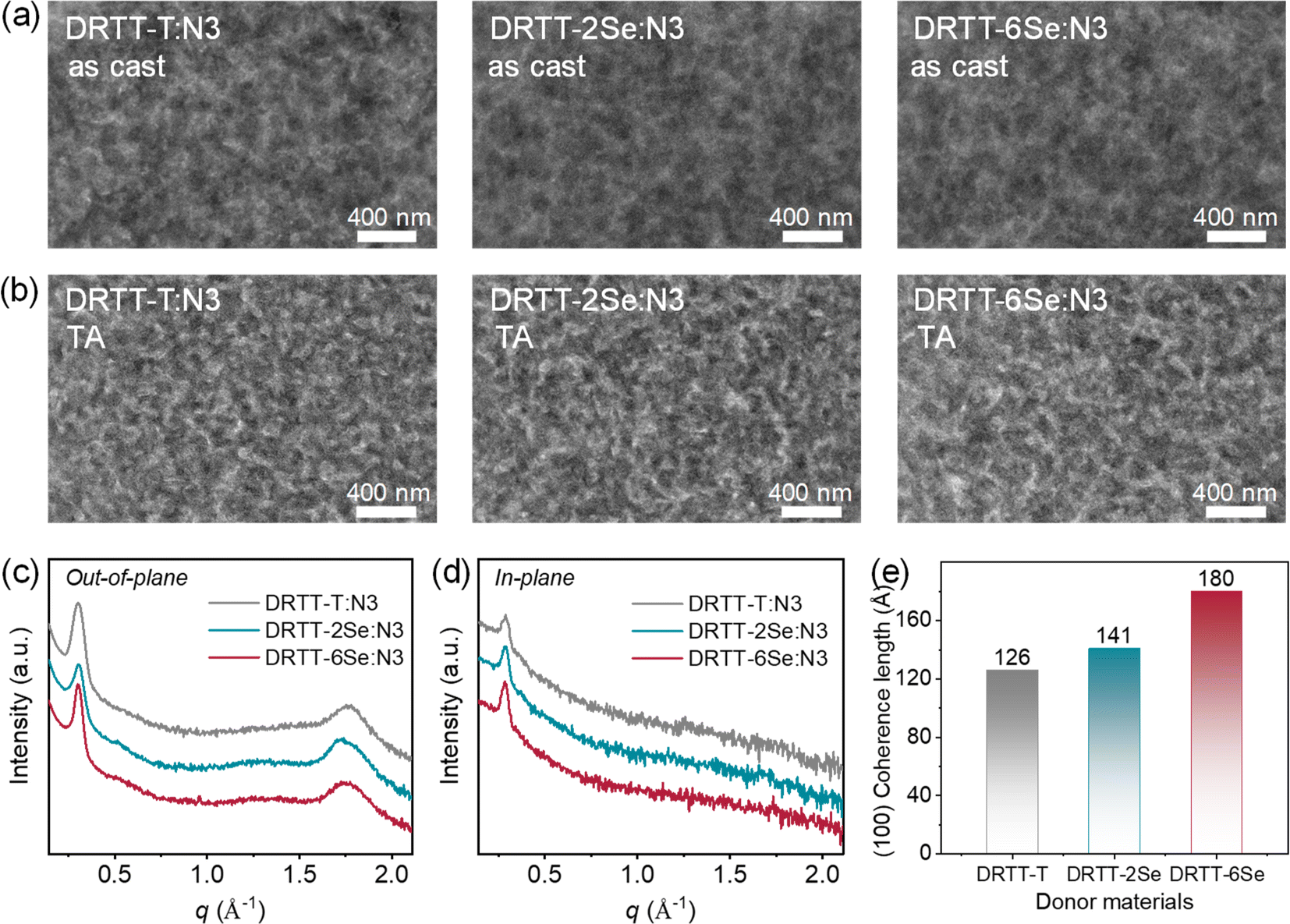 | ||
| Fig. 5 (a and b) TEM images of the blend films without (a) and with TA treatments (b). TEM images (b). (c and d) XRD patterns of the optimal blend films in the out-of-plane (c) and in-plane directions (d). (e) The CCL values derived from the out-of-plane (100) diffraction peaks of the optimal blend films. | ||
3. Conclusion
In summary, two “twisted” small molecule donors with alkylselenophenyl side chains, namely DRTT-2Se and DRTT-6Se, were synthesized and compared with their alkyl thiophenyl substituted analogue DRTT-T. The “twisted” skeletons of the molecules can suppress excessive phase separation caused by molecular crystallization during the film forming process, and the strong intermolecular interactions encourage the planarization of the molecular skeletons in the condensed state. Through replacement of alkylthiophenyl with alkylselenophenyl side chains, the further enhanced intermolecular interactions allow the molecules to form more ordered molecular packing in films under suitable post-annealing conditions without causing an increase in the phase separation scale, thus delivering more efficient charge transport and reduced charge recombination. In addition, the upshifted HOMO levels of DRTT-2Se and DRTT-6Se provide a larger driving force for the dissociation of the excitons generated in N3, leading to higher EQE in the devices. Thus, DRTT-2Se and DRTT-6Se based OSCs exhibited higher Jsc and FF, and the device performance was less sensitive to the thickness of the active layers. Besides, the upshifted HOMO levels of DRTT-2Se and DRTT-6Se do not lead to decreased Voc, which could be related to the reduced nonradiative loss and lower energetic disorder for DRTT-2Se and DRTT-6Se based devices, probably derived from the enhanced intermolecular interactions and improved molecular ordering. The enhanced Jsc and FF as well as the unchanged Voc gave rise to significant improvement in device performance for alkylselenophenyl substituted molecules. Owing to the appropriate film morphology with highest molecular ordering, DRTT-6Se with alkylselenophenyl side chains on both the TT central unit and BDT π bridges displayed the best device efficiency exceeding 15%, and the PCE of DRTT-6Se based ASM-OSCs retained 92% of the optimal value when the thickness of the active layer increased to ∼300 nm, which is rare for the ASM-OSCs reported so far. This study demonstrates that the molecular design strategy based on the combination of “twisted” backbones and strongly interacting building blocks is effective for achieving suitable film microstructures and hence yielding high-efficiency ASM-OSCs with good film thickness tolerance.Author contributions
Miaomiao Li conceived the idea. Miaomiao Li and Wang Ni designed the experiments. Xiafei Cheng synthesized the materials, performed the UV-vis/CV/DSC/SCLC/TEM/XRD measurements, and fabricated the solar cells. Ziqi Liang and Xuwen Zhang performed PL/TPV/TPC measurements. Shifeng Liang, Yan Xu and Jie Xu performed EQEEL/sEQE measurements. Miaomiao Li and Xiafei Cheng analyzed the data and wrote the manuscript with input from Yanhou Geng and Wang Ni. All authors provided comments on the manuscript and contributed to the editing.Conflicts of interest
There are no conflicts to declare.Acknowledgements
The authors acknowledge the National Key R&D Program of China (no. 2022YFB4200400), and the National Natural Science Foundation of China (no. 22075200).References
- G. Yu, J. Gao, J. C. Hummelen, F. Wudl and A. J. Heeger, Science, 1995, 270, 1789 CrossRef CAS.
- R. F. Service, Science, 2011, 332, 293 CrossRef CAS PubMed.
- G. Li, R. Zhu and Y. Yang, Nat. Photonics, 2012, 6, 153–161 CrossRef CAS.
- S. D. Collins, N. A. Ran, M. C. Heiber and T.-Q. Nguyen, Adv. Energy Mater., 2017, 7, 1602242 CrossRef.
- Y. Huo, H.-L. Zhang and X. Zhan, ACS Energy Lett., 2019, 4, 1241–1250 CrossRef CAS.
- B. Kan, Y. Kan, L. Zuo, X. Shi and K. Gao, InfoMat, 2020, 3, 175–200 CrossRef.
- Y. Lin, Y. Li and X. Zhan, Chem. Soc. Rev., 2012, 41, 4245–4272 RSC.
- H. Bin, J. Wang, J. Li, M. M. Wienk and R. A. J. Janssen, Adv. Mater., 2021, 33, e2008429 CrossRef PubMed.
- H. Gao, Y. Sun, L. Meng, C. Han, X. Wan and Y. Chen, Small, 2023, 19, e2205594 CrossRef PubMed.
- J. Jin, Q. Wang, K. Ma, W. Shen, L. A. Belfiore, X. Bao and J. Tang, Adv. Funct. Mater., 2023, 2213324, DOI:10.1002/adfm.202213324.
- B. Qiu, Z. Chen, S. Qin, J. Yao, W. Huang, L. Meng, H. Zhu, Y. M. Yang, Z. G. Zhang and Y. Li, Adv. Mater., 2020, 32, e1908373 CrossRef PubMed.
- X. Wang, J. Wang, J. Han, D. Huang, P. Wang, L. Zhou, C. Yang, X. Bao and R. Yang, Nano Energy, 2021, 81, 105612 CrossRef CAS.
- X. Yuan, H. Chen, S. Kim, Y. Chen, Y. Zhang, M. Yang, Z. Chen, C. Yang, H. Wu, X. Gao, Z. Liu and C. Duan, Adv. Energy Mater., 2023, 2204394, DOI:10.1002/aenm.202204394.
- Y.-Z. Zhang, N. Wang, Y.-H. Wang, J.-H. Miao, J. Liu and L.-X. Wang, Chin. J. Polym. Sci., 2022, 40, 989–995 CrossRef CAS.
- R. Zhou, Z. Jiang, Y. Shi, Q. Wu, C. Yang, J. Zhang, K. Lu and Z. Wei, Adv. Funct. Mater., 2020, 30, 2005426 CrossRef CAS.
- H. Tang, C. Yan, J. Huang, Z. Kan, Z. Xiao, K. Sun, G. Li and S. Lu, Matter, 2020, 3, 1403–1432 CrossRef.
- W. Ye, Y. Yang, Z. Zhang, Y. Zhu, L. Ye, C. Miao, Y. Lin and S. Zhang, Sol. RRL, 2020, 4, 2000258 CrossRef CAS.
- H. Bin, I. Angunawela, B. Qiu, F. J. M. Colberts, M. Li, M. J. Dyson, M. M. Wienk, H. Ade, Y. Li and R. A. J. Janssen, Adv. Energy Mater., 2020, 10, 2001589 CrossRef CAS.
- X. Cheng, M. Li, Z. Liang, M. Gao, L. Ye and Y. Geng, ACS Appl. Energy Mater., 2021, 4, 8442–8453 CrossRef CAS.
- K. Gao, W. Deng, L. Xiao, Q. Hu, Y. Kan, X. Chen, C. Wang, F. Huang, J. Peng, H. Wu, X. Peng, Y. Cao, T. P. Russell and F. Liu, Nano Energy, 2016, 30, 639–648 CrossRef CAS.
- A. Sharenko, M. Kuik, M. F. Toney and T.-Q. Nguyen, Adv. Funct. Mater., 2014, 24, 3543–3550 CrossRef CAS.
- O. K. Kwon, J.-H. Park, D. W. Kim, S. K. Park and S. Y. Park, Adv. Mater., 2015, 27, 1951–1956 CrossRef CAS PubMed.
- H. Li, Q. Wu, R. Zhou, Y. Shi, C. Yang, Y. Zhang, J. Zhang, W. Zou, D. Deng, K. Lu and Z. Wei, Adv. Energy Mater., 2018, 1803175, DOI:10.1002/aenm.201803175.
- Y. Wang, Y. Wang, L. Zhu, H. Liu, J. Fang, X. Guo, F. Liu, Z. Tang, M. Zhang and Y. Li, Energy Environ. Sci., 2020, 13, 1309–1317 RSC.
- L. Yang, S. Zhang, C. He, J. Zhang, H. Yao, Y. Yang, Y. Zhang, W. Zhao and J. Hou, J. Am. Chem. Soc., 2017, 139, 1958–1966 CrossRef CAS PubMed.
- S. Zhang, L. Yang, D. Liu, C. He, J. Zhang, Y. Zhang and J. Hou, Sci. China: Chem., 2018, 60, 1340–1348 CrossRef.
- J. Cao, H. Wang, S. Qu, J. Yu, L. Yang, Z. Zhang, F. Du and W. Tang, Adv. Funct. Mater., 2020, 2006141, DOI:10.1002/adfm.202006141.
- X. Dong, K. Yang, H. Tang, D. Hu, S. Chen, J. Zhang, Z. Kan, T. Duan, C. Hu, X. Dai, Z. Xiao, K. Sun and S. Lu, Sol. RRL, 2020, 4, 1900326 CrossRef CAS.
- R. Noriega, J. Rivnay, K. Vandewal, F. P. V. Koch, N. Stingelin, P. Smith, M. F. Toney and A. Salleo, Nat. Mater., 2013, 12, 1038–1044 CrossRef CAS PubMed.
- L. Ye, Y. Xiong, M. Zhang, X. Guo, H. Guan, Y. Zou and H. Ade, Nano Energy, 2020, 77, 105310 CrossRef CAS.
- L. Zhu, M. Zhang, G. Zhou, T. Hao, J. Xu, J. Wang, C. Qiu, N. Prine, J. Ali, W. Feng, X. Gu, Z. Ma, Z. Tang, H. Zhu, L. Ying, Y. Zhang and F. Li, Adv. Energy Mater., 2020, 1904234, DOI:10.1002/aenm.201904234.
- X. Cheng, M. Li, Z. Guo, J. Yu, G. Lu, L. Bu, L. Ye, H. Ade, Y. Chen and Y. Geng, J. Mater. Chem. A, 2019, 7, 23008–23018 RSC.
- L. Huo, S. Zhang, X. Guo, F. Xu, Y. Li and J. Hou, Angew. Chem., Int. Ed., 2011, 50, 9697–9702 CrossRef CAS PubMed.
- X. Dong, H. Tian, Z. Xie, Y. Geng and F. Wang, Polym. Chem., 2017, 8, 421–430 RSC.
- J. He, Z. Liang, L. Lin, S. Liang, J. Xu, W. Ni, M. Li and Y. Geng, Polymer, 2023, 274, 125890 CrossRef CAS.
- M. Scheuble, Y. M. Gross, D. Trefz, M. Brinkmann, J. T. L. Navarrete, M. C. R. Delgado and S. Ludwigs, Macromolecules, 2015, 48, 7049–7059 CrossRef CAS.
- R. S. Ashraf, I. Meager, M. Nikolka, M. Kirkus, M. Planells, B. C. Schroeder, S. Holliday, M. Hurhangee, C. B. Nielsen, H. Sirringhaus and I. McCulloch, J. Am. Chem. Soc., 2015, 137, 1314–1321 CrossRef CAS PubMed.
- F.-Y. Cao, F.-Y. Lin, C.-C. Tseng, K.-E. Hung, J.-Y. Hsu, Y.-C. Su and Y.-J. Cheng, ACS Appl. Mater. Interfaces, 2019, 11, 11674–11683 CrossRef CAS PubMed.
- G. Chai, J. Zhang, M. Pan, Z. Wang, J. Yu, J. Liang, H. Yu, Y. Chen, A. Shang, X. Liu, F. Bai, R. Ma, Y. Chang, S. Luo, A. Zeng, H. Zhou, K. Chen, F. Gao, H. Ade and H. Yan, ACS Energy Lett., 2021, 5, 3415–3425 CrossRef.
- F. Lin, K. Jiang, W. Kaminsky, Z. Zhu and A. K.-Y. Jen, J. Am. Chem. Soc., 2020, 142, 15246–15251 CrossRef CAS PubMed.
- T. Xu, J. Lv, K. Yang, Y. He, Q. Yang, H. Chen, Q. Chen, Z. Liao, Z. Kan, T. Duan and S. Lu, Energy Environ. Sci., 2021, 14, 5366–5376 RSC.
- K. Jiang, Q. Wei, J. Y. L. Lai, Z. Peng, H. K. Kim, J. Yuan, L. Ye, H. Ade, Y. Zou and H. Yan, Joule, 2019, 3, 3020–3033 CrossRef CAS.
- Z.-G. Zhang, B. Qi, Z. Jin, D. Chi, Z. Qi, Y. Li and J. Wang, Energy Environ. Sci., 2014, 7, 1966–1973 RSC.
- S. Karuthedath, J. Gorenflot, Y. Firdaus, N. Chaturvedi, C. S. P. D. Castro, G. T. Harrison, J. I. Khan, A. Markina, A. H. Balawi, T. A. D. Peña, W. Liu, R.-Z. Liang, A. Sharma, S. H. K. Paleti, W. Zhang, Y. Lin, E. Alarousu, S. Lopatin, D. H. Anjum, P. M. Beaujuge, S. D. Wolf, I. McCulloch, T. D. Anthopoulos, D. Baran, D. Andrienko and F. Laquai, Nat. Mater., 2021, 20, 378–384 CrossRef CAS PubMed.
- Z. Liang, J. He, B. Zhao, M. Gao, Y. Chen, L. Ye, M. Li and Y. Geng, Sci. China: Chem., 2022, 66, 216–227 CrossRef.
- A. Baumann, J. Lorrmann, D. Rauh, C. Deibel and V. Dyakonov, Adv. Mater., 2012, 24, 4381–4386 CrossRef CAS PubMed.
- A. Maurano, R. Hamilton, C. G. Shuttle, A. M. Ballantyne, J. Nelson, B. O'Regan, W. Zhang, I. McCulloch, H. Azimi, M. Morana, C. J. Brabec and J. R. Durrant, Adv. Mater., 2010, 22, 4987–4992 CrossRef CAS PubMed.
- F. Urbach, Phys. Rev., 1953, 92, 1324 CrossRef CAS.
- X. Zhang, L. Qin, Y. Li, J. Yu, H. Chen, X. Gu, Y. Wei, X. Lu, F. Gao and H. Huang, Adv. Funct. Mater., 2022, 32, 2112433 CrossRef CAS.
- J. Zhou, D. He, Y. Li, F. Huang, J. Zhang, C. Zhang, Y. Yuan, Y. Lin, C. Wang and F. Zhao, Adv. Mater., 2023, 35, e2207336 CrossRef PubMed.
- W. Feng, S. Wu, H. Chen, L. Meng, F. Huang, H. Liang, J. Zhang, Z. Wei, X. Wan, C. Li, Z. Yao and Y. Chen, Adv. Energy Mater., 2022, 12, 2104060 CrossRef CAS.
- Y. Li, D. Qian, L. Zhong, J.-D. Lin, Z.-Q. Jiang, Z.-G. Zhang, Z. Zhang, Y. Li, L.-S. Liao and F. Zhang, Nano Energy, 2016, 27, 430–438 CrossRef CAS.
- S. Liu, J. Yuan, W. Deng, M. Luo, Y. Xie, Q. Liang, Y. Zou, Z. He, H. Wu and Y. Cao, Nat. Photonics, 2020, 14, 300–305 CrossRef CAS.
- Z. Zhang, Y. Li, G. Cai, Y. Zhang, X. Lu and Y. Lin, J. Am. Chem. Soc., 2020, 142, 18741–18745 CrossRef CAS PubMed.
Footnote |
| † Electronic supplementary information (ESI) available. See DOI: https://doi.org/10.1039/d3ta01893h |
| This journal is © The Royal Society of Chemistry 2023 |