
 Open Access Article
 This Open Access Article is licensed under a
 Creative Commons Attribution 3.0 Unported Licence
Redox-active oxygen in oxides: emergent applications, including field-induced resistive switching, flash luminescence, p–n junctions and high capacity battery cathodes
Anthony R.
West
 *
*
University of Sheffield, Department of Materials Science & Engineering, Mappin St., Sheffield S1 3JD, UK. E-mail: a.r.west@sheffield.ac.uk
First published on 5th May 2023
Abstract
Oxide ions are traditionally regarded as forming the inert anion sub-lattice of oxide structures whose properties are largely dominated by the cations present. This viewpoint is being increasingly challenged by examples of a diverse range of phenomena in which some of the oxide ions present are redox-active. The source of this activity in ionic structures is the inherent instability of O2− ions in the gas phase which are stabilised in crystal lattices by the additional lattice energy associated with doubly-charged anions. Oxide ions located either at sample surfaces or adjacent to lower valence (acceptor) substitutional cations, may not be fully stabilised, as they are surrounded by an effective positive charge of less than 2+. They are under-bonded and may ionise, either spontaneously or with reduced ionisation potential. Examples of oxygen redox include: high capacity Li and Na battery cathodes in which there is insufficient redox-active transition metal component present to account for the observed charge/discharge capacities; electroceramic materials such as some doped titanate perovskites which exhibit hopping p-type conductivity and in which the only realistic location of the electron holes is on lattice oxide ions; novel resistive switching phenomena and insulator-metal transitions in oxide ceramics; resistance degradation of insulating ceramics prior to dielectric breakdown; flash luminescence by creation of p–n junctions in oxide ceramics; possible origin of 2-dimensional electron gases in layered superlattices formed from oxide insulators. The underlying principles of oxygen redox activity are set out and its possible contribution to emergent phenomena are discussed.
10th anniversary statementIt has been my enormous good fortune and privilege to be involved with the royal society of chemistry and its expanding materials chemistry activities. I was the first scientific editor and Chairman of the materials editorial board, MEB of the Journal of Materials Chemistry in 1991, co-authored three papers in the first issue, was honoured with a special issue of J. Mater. Chem. A in April 2018 and am delighted now to contribute to this anniversary issue. In the formative years of the journal, driven by the enthusiasm, insight and forward thinking of MEB members, a series of International Conferences in Materials Chemistry were started, with MC1 in Aberdeen, 1995 and now, MC16 scheduled for Dublin in summer 2023. A series of materials discussions, based on faraday discussions, was started with the first, MD1 in Bordeaux, France. With such continuing successes, it was not long before the Materials Chemistry Forum of the RSC was created, again driven by MEB, by informally linking various RSC and non-RSC materials subject groups, which subsequently evolved into the fully-fledged Materials Chemistry Division of the RSC. Materials Chemistry is now recognised internationally with IUPAC acceptance (P. Day, L. V. Interrante and A. R. West, Pure. Appl. Chem., 2009, 81, 1707) of the definition ‘Materials Chemistry comprises the application of chemistry to the design, synthesis, characterisation, processing, understanding and utilisation of materials, particularly those with useful, or potentially useful, physical properties’. This definition encapsulates the original motivation to create the interdisciplinary, but chemistry-based, J. Mater. Chem. and its continuation in the follow-on journals J. Mater. Chem. A, B and C. |
1. Introduction
1.1. Oxygen valency in oxides
The doubly-charged oxygen anion, O2−, is unstable in the gas phase and should ionise spontaneously to give the O− ion, as shown by first and second electron affinity data for atomic oxygen, Table 1. It does not ionise in crystal lattices, however, because the increased lattice energy associated with structures based on O2− ions compared with those based on O− ions, more than offsets the positive electron affinity of the reaction:| O− + e− = O2− | (1) |
| Reaction | ΔH, kJ mol−1 |
|---|---|
| O(g) + e− = O−(g) | −141 |
| O−(g) + e− = O2−(g) | +844 |
Consequently, it is standard practice to regard crystalline oxides as based on divalent oxygen leading to an ionic bonding model which has been, and continues to be, very successful in the description and classification of solid oxide structures. It is accepted that, in reality, most structures are not entirely ionic and bond descriptions often take partial covalency into account; nevertheless, the component atoms have clearly identifiable valences or oxidation states that are the same as those for purely ionic structures. In the case of transition metal oxides that show high electronic conductivity, some of the outermost electrons are delocalised in energy bands and the concept of atom valence for both cations and anions may then become less useful, especially when the band structure is described in terms of hybridised cation and anion orbitals.
Since the gas phase O2− ion is spontaneously unstable, the question arises as to whether there any situations in which ionisation of O2− ions in oxide lattices can occur, either spontaneously or with reduced ionisation potential. This would require those oxide ions to be under-bonded by a deficit in the effective amount of positive charge of the surrounding cations, leading to reduction in local stabilisation energy of those O2− ions. Pauling's electrostatic valence rule1 provides the classic guide to under- and over-bonded oxide ions and is extended more generally to structures that are complex or have distributions in bond lengths by Brown's bond valence sum, bvs calculations.2 It is usually the case, however, that local electroneutrality holds in oxide structures, in which case there is no reason to expect any significant under- (or over-) bonding of oxide ions; indeed, bvs calculations are often used as a confirmatory test on the validity of proposed crystal structure details.
Two situations may be envisaged where under-bonding is present. First, at oxide surfaces, oxide ions are co-ordinatively unsaturated if oxygen atoms in the outermost layer are not fully surrounded by cations. This is particularly the case for structures that have alternating layers of cations and anions which are parallel to a particular crystal surface; if the outermost layer consists of oxide ions, then no more than half of the coordination sphere around a particular oxygen contains cations. There are many examples in the literature of solid surfaces in which oxygen species are present in reduced valence states, such as peroxide, O22−, superoxide, O2− and O− ions, even though these species may not be present in crystal interiors. We may conclude from the literature that it is commonplace for such species to be present at oxide surfaces, even though their presence can usually be detected only by high vacuum spectroscopic studies of clean crystal surfaces.
Second, in acceptor-doped oxides in which some cations of the host structure are replaced by those of a lower valence cation, such as Ti4+ replaced partially by Mg2+ in BaTiO3 perovskite, neighbouring oxide ions may be under-bonded. Thus, in BaTiO3, any oxide ion has only two Ti4+ cations as its nearest neighbours because the structure consists of corner-sharing TiO6 octahedra; if one of these Ti4+ ions is replaced by Mg2+, that oxide ion becomes significantly under-bonded.3 Relaxation of the local structure in the vicinity of the dopant cation may help to relieve the under-bonding and restore local electro-neutrality; alternatively, this may be achieved if the under-bonded oxide ion can ionise to give an O− ion.
1.2. Evidence for oxygen redox activity
Direct detection of the presence of a small number of O− ions in a lattice that consists predominantly of O2− ions is difficult. Indirectly, however, this may lead to significant changes in electrical conductivity because the O− ions can act as a source of electron holes. Undoped materials such as stoichiometric BaTiO3 are insulating but become modest p-type semiconductors when acceptor-doped.3–8 This may be represented by a general equation that does not specify the location of holes, such as for Mg-doped BaTiO3: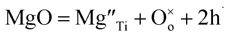 | (2) |
Using Kroger–Vink notation,  refer respectively to: Mg occupying a Ti site with nominal net charge 2− as the Mg site is now over-bonded; a lattice oxygen with no net charge; positively-charged electron holes. A wide range of similar acceptor-doped materials exhibit thermally-activated p-type conductivity, Table 2. The location of the holes responsible for conductivity was traditionally attributed to impurities19 such as Fe3+ which could ionise to Fe4+. The location is now believed to be on lattice oxide ions, in part because high purity chemicals were used for the syntheses, Table 2 and it is unlikely that a significant amount of Fe impurities would be present in a range of samples made in different laboratories and using different reagents, but also because the other cations in the structure are already in their highest valence states and cannot be considered as a possible location for the holes.
| p-Type material | Reference |
|---|---|
| Ba(Ti1−xMgx)O3−x: x = 0.00003 to 0.01 | 3 |
| Ba(Ti1−xZnx)O3−x: x = 0.00003 to 0.01 | 4 |
| Ba(Ti1−xCax)O3−x: x = 0.01, 0.03 | 5 |
| BaTiO3, Ba-rich and Ti-rich | 6 |
| Ca(Ti1−xZnx)O3−x: x = 0.05–0.07 | 7 |
| Sr(Ti1−xMgx)O3−x: x = 0.005, 0.01 | 8 |
| (Bi1−xCax)FeO3−x/2: x = 0.03, 0.05, 0.30 | 9 and 10 |
| Ba1−xSrxTiO3−δ: x = 0.2 | 11 |
| Zr1−xYxO2−x/2 | 12–15 |
| Hf1−xYxO2−x/2: y = 0.15–0.40 | 16 and 17 |
| Ca0.15Zr0.85O1.85 | 18 |
| Al2O3: Mg | 18 |
For convenience, the oxidised, but charged, oxygen species responsible for hole location and redox activity of oxygen are referred to here as O− ions, especially in materials for which the bonding is primarily ionic. Some authors refer more generally to oxidised oxide anions as On− or O2n− species and evidence for ionised diatomic species such as peroxide and superoxide is obtained from surface spectroscopy studies. Such polyatomic species are more likely to be encountered at sample surfaces rather than in sample interiors due to size constraints imposed by the regular periodicity of crystal lattices. One known exception concerns spectroscopic evidence for superoxide ions in ceramics of Ca-doped BaTiO3 with Ti substituted by Ca, which was annealed in O2.20 This was attributed to the combined presence of oxygen vacancies and the large Ca2+ acceptor dopant which together, allowed O22− ions to be incorporated into the BaTiO3 lattice. In the absence of unambiguous identification of the charged oxygen species in most studies, they are referred to here, therefore, as O− ions.
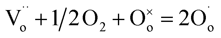
Additional experimental observations that point to the location of holes on under-bonded oxygen are the increases in p-type conductivity in acceptor-doped materials with increasing oxygen partial pressure, pO2 in the surrounding atmosphere, Fig. 1. The explanation is that oxygen molecules dissociate and ionise by a redox reaction that generates both oxygen anions from the O2 molecules and holes. Under-bonded oxide ions are the source of electrons to reduce the O2 molecules but also then become a location for holes. Oxygen anions arising from the ionised O2 molecules occupy vacant lattice oxygen sites generated by the acceptor doping charge compensation mechanism, giving the overall idealised reaction:
 | (3) |
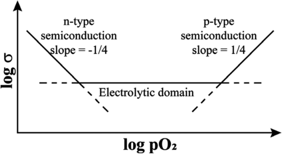 | ||
| Fig. 1 Schematic ionic and electronic conductivity domains as a function of pO2. | ||
 refers to a doubly-charged oxygen vacancy.
  refers to an ionised lattice oxide ion, i.e., an oxide ion with a hole, which is the same as an O− ion in the presence of a majority of lattice O2− ions. The
  ions in eqn (3) arise simultaneously from two sources therefore: (i) ionisation of existing under-bonded lattice oxide ions that are either at the sample surface or in the vicinity of acceptor dopants and (ii) reduction of incoming oxygen molecules that dissociate and whose ionisation is limited to the first step because of the positive electron affinity associated with the second step in double ionisation, eqn (1). Stoichiometric materials such as undoped BaTiO3 (ref. 6) shows very little p-type conductivity for two reasons: the number of under-bonded oxide ions is much reduced and there are very few available oxygen vacancies.
Reaction (3) leads to an increase in the number of holes (on oxygen) and an increase in p-type conductivity. The O− ions themselves are current carriers by virtue of electron exchange with surrounding O2− ions. Temperature-dependent conductivity measurements show that the p-type conductivity is an activated process which means that the holes are localised, on oxygen, rather than in a delocalised energy band for which little or no thermal activation of conductivity would be expected. The increase in conductivity with increasing pO2 confirms that the current carriers are holes.
The above considerations apply most simply and unambiguously to oxides that contain cations in their highest oxidation states, such as many of those listed in Table 2, leaving oxygen as the only possible location for holes in the absence of stray, redox-active impurities. However, in oxides containing transition metal cations such as Fe3+, Co3+ and Ni2+ and especially those containing mixed valence cations, holes may in principle be located on either the transition metal, or oxygen or indeed, delocalised in a band structure composed of hybrid orbitals. It is well-established that in metallic oxides such as some of the cuprate superconductors, band structures form by hybridisation of cation 3d and oxygen 2p orbitals; these materials are frequently referred to as hole conductors although the carriers are delocalised.
Under certain circumstances, acceptor-doped materials may also be oxide ion conductors by virtue of the oxygen vacancies that are created as a result of charge compensation. For the titanate materials summarised in Table 2, the level of p-type conductivity greatly exceeds that of any oxide ion conductivity, but in other perovskites such as Ca-doped BiFeO3, high levels of both oxide ion and p-type conductivity are observed, depending on pO2 during synthesis and impedance measurements.9,10 It is clearly important to distinguish between oxide ion and electronic conductivity; methodologies for this are available but are beyond the scope of this review.
In contrast to the p-type conductivity of acceptor-doped oxides discussed so far, donor-doped oxides may show n-type conductivity especially when, at lower pO2, they lose a small amount of oxygen during high temperature processing, Fig. 1. As discussed later, n-type conductivity is an essential component of both resistive switching and flash phenomena, particularly in materials that can be either p-type or n-type, depending on circumstances. Oxygen loss and the generation of electrons occurs by double ionisation of lattice oxide ions and their recombination to form O2 molecules.
| O2− = 1/2O2 + 2e | (4) |
Evidence for oxygen loss is provided by direct measurements of weight changes or can be deduced from an observed increase of conductivity in atmospheres of reduced pO2 since eqn (4) is displaced to the right, as shown at low pO2 in Fig. 1.
1.3. Partial or complete ionisation of O2− ions
Conventionally, reduction of O2 gas molecules to O2− ions, or the reverse process, eqn (4), is treated as a single step process. In some cases, especially those discussed here in which there is evidence for p-type conductivity or anion redox activity in battery cathodes, it is necessary to break eqn (4) into two stages:| O2− = O− + e | (5) |
| O− = 1/2O2 + e | (6) |
Formation of O− ions and the consequences for subsequent properties and sample characteristics, depend on this partial ionisation of O2− ions, eqn (5), as a separate first step. For instance, in order to take advantage of anion redox in high capacity reversible battery cathodes, ionisation should be limited to step (5) otherwise, irreversible oxygen loss, eqn (6), is likely to occur. In flash sintering and related phenomena, the flash appears to be associated, at least in part, with energy release by defect annihilation or charge recombination processes and one possible mechanism involves recombination of electrons and holes at a p–n junction. This would, therefore, require separate mechanisms, such as eqn (5) and (6), for the generation of both holes and electrons in a particular material, as discussed later.
1.4. Gas–solid equilibria at oxide surfaces
At a typical solid oxide surface, numerous equilibria and ionic species may be envisaged, as summarised by:| O2(gas) = O2(ads) = O2− = O22−/2O− = 2O2−(surface) = 2O2−(bulk) | (7) |
The middle three equilibria are all redox half-reactions. They can be displaced to either the left or the right by reacting with electrons or holes. There are several possible sources of electrons. They could be (i) ‘free’ electrons that are already present within n-type samples, (ii) electrons that result from a separate half-reaction or (iii) electrons injected from a negative electrode. The equilibria are sensitive to changes in pO2. They can also be displaced by an applied voltage in which the response is different at the negative and positive electrodes. Changes to the equilibria in eqn (7) can have a direct effect on electrical properties, therefore, since the electrons that take part in the equilibria may either be withdrawn from, or injected into, the underlying sample. Such surface reactions can modify the electrical properties of a bulk sample and also give insight into conduction mechanisms.
At this point, it is worth noting a parallel between eqn (7) and the very extensive studies of catalytic processes, such as those involved in oxygen evolution reactions, OER21 for electricity-driven water splitting. A series of steps and intermediates are identified in proton–electron transfer reactions in which oxygen is redox-active and changes from the 2-state in OH− ions, via intermediates that also include polyatomic species, to give O2 molecules by the overall reaction:
| 2OH− = O2 + 2H+ + 4e | (8) |
This review does not include any further consideration of catalysed OER and ORR reactions, apart from noting the two-step nature of oxygen redox, eqn (5) and (6), and the likely presence of under-bonded oxygens at nanoparticle oxide catalyst surfaces. Gas–solid redox equilibria involving O2 molecules and under-bonded lattice oxide ions, eqn (3), may be relevant to the lattice oxygen mechanism (LOM) of OER in which, using isotope labelling mass spectrometry, lattice oxygens are found to be present in released O2 molecules.21 Catalytic activity of perovskites such as La1−xSrxCoO3−δ and related Ruddlesden–Popper phases, La0.5Sr1.5Ni1−xFexO4−δ is very dependent on composition x and usually attributed to transition metal–oxygen covalency effects; the presence of under-bonded oxygens associated with the aliovalent substitution of Sr for La may also be a factor.
1.5. Effect of applied voltage on electrical properties
Depending on the magnitude of an applied voltage, a range of phenomena may be observed. Small voltages of e.g., 100 mV or less, are sufficient to apply a slight bias to the random thermal motions of electrons or ions but not to cause any changes to structure or electrical properties. This underpins the use of conductivity/impedance measurements in which a small signal sinusoidal voltage is not expected to cause changes to the electrical properties or structure/composition of a material. With increasing voltage, the equilibria in eqn (7) may be displaced and for instance, the resulting gas–solid surface exchange reactions may lead to changes in electron/hole concentrations in sample interiors which have a significant impact on measured electrical properties. These processes are an essential feature of the operation of electrodes in fuel cells, gas sensors, catalysts and other electrochemical processes.Voltages that exceed a few volts are above the theoretical decomposition potential of any sample and would take samples outside their zone of thermodynamic stability. In practice, decomposition may be prevented if there is a large activation barrier to decomposition, or over-potential, that effectively gives kinetic stability to a sample in the presence of an applied voltage. Two examples of present interest, with high application possibilities, are resistive switching of memristors and flash sintering of ceramics. Their study is opening up emerging research possibilities in which materials are placed outside their zone of thermodynamic stability but are comfortably within a domain of kinetic stability.
A complete understanding of the combined effect of an applied voltage and changing pO2 on electrical properties requires information on the various equilibria shown in eqn (7) with the additional complication that changes induced at the positive and negative electrodes by an applied voltage are likely to differ. At a positive electrode, the various equilibria 2–4, eqn (7), may be displaced to the left and cause partial or complete ionisation of oxide ions. For complete ionisation and evolution of O2 molecules at the positive electrode, the electrons that are released may be re-injected into the sample at the negative electrode. This result is similar to the widely-observed n-type conductivity which arises when certain ceramic oxides lose O2 at high temperatures although in that case, there is no applied voltage and loss of O2 accompanied by electron injection can occur anywhere on the sample surface.
For partial ionisation of (underbonded) O2− ions in which equilibria 4, eqn (7), are driven to the left, both holes and electrons are generated. Holes are O− ions or other partially-oxidised oxygen species. The ionised electrons may be trapped at the positive electrode, as in the charging of a capacitor.15 Or, they may reduce (and cause dissociation of) O2 molecules, reverse of reaction (6), similar to the effect of pO2 on acceptor-doped materials in the absence of an applied voltage, eqn (3). The ionised electrons may also be injected at the negative electrode.
Many of the studies cited below involve the application of voltages in the range 0.5–40 V across millimetre-thick solid samples (and therefore with field gradients of 5–400 V cm−1) to which 2-terminal electrodes of Au or Pt are attached. Usually, a constant voltage is applied at a set temperature at the same time as electrical properties, which may be time-dependent, are measured using impedance spectroscopy. Some of the processes involve single ionisation only of O2− ions, eqn (5). Others involve both ionisation steps and in some cases, depending on the magnitude of the voltage, the two steps are clearly separated and have different consequences.
2. Overview of research developments involving oxygen redox activity
2.1. p- and n-type conductivity
It is convenient to commence with the effect of small voltages on structures that are ionically-bonded since the results are straightforward and help to identify the factors that need to be considered in evaluating the effects of higher voltages which also involve gas–solid interactions. The effect of pO2 alone, in the absence of an applied voltage, on materials that are primarily oxide ion conductors but can lead to varying degrees of either n-type or p-type electronic conductivity is summarised schematically in Fig. 1. In the electrolytic domain, oxide ion conduction is predominant and the range of pO2 values that cover this domain is vitally important for materials that are used as solid electrolytes with negligible electronic conductivity. A small applied voltage has almost no effect on the overall conductivity in this domain.At lower pO2, materials show increasing degrees of n-type electronic conductivity associated with sample reduction and oxygen loss, represented ideally by reaction (4). There are many such examples and studies in the literature of this behaviour in, for instance, easily reduced Ce-based or Bi-based oxides, since it is possible to control and measure pO2 values over a very wide range below atmospheric pressure. In order to explain the n-type behaviour associated with oxygen loss, it is not necessary to consider possible involvement of the intermediate O− state of oxygen since double ionisation of O2− ions and liberation of O2 gas can account for the observed n-type behaviour.
At higher pO2 and to explain p-type behaviour, however, consideration of the O− state as the location of holes is essential. Although measurements are limited by the difficulty in obtaining and controlling pressures over a wide range above atmospheric, there are sufficient data in the literature to show that the onset of the p-type region, Fig. 1, is a common phenomenon, especially in acceptor-doped materials. The effect of pO2 in this region can be treated in terms of eqn (3) and is based on two assumptions: (i) the structures do not contain variable valence transition metal ions; (ii) the holes are not itinerant but are localised and therefore, lattice oxygens are the only possible location for the holes, as O− ions.
For materials that are modest extrinsic semiconductors, such as those listed in Table 2, the effect of an increase in pO2 on electrical conductivity provides a simple method to show whether the electronic charge carriers are electrons or holes, i.e., n- or p-type. If the carriers are n-type, the conductivity decreases:
| 1/2O2 + 2e− = O2− | (9) |
Several acceptor-doped titanate perovskites, Table 2, show increasing p-type conductivity with increasing voltage. The increases are variously temperature-, time- and voltage-dependent, as shown for ceramic pellets of BaTi0.99O2.98 in Fig. 2.6 Usually temperatures above 150 °C are required in order to see any significant voltage-dependence, but with increasing temperature, conductivity increases are greater and occur more rapidly (a). Conductivity increases have been observed with fields as low as 0.76 V mm−1 but again, are greater with increasing fields (b and c). The effect of increasing both temperature and voltage can give conductivity increases of up to three orders of magnitude (a–c); the increases are reversible, but also are time-dependent, on removing the bias, (d).
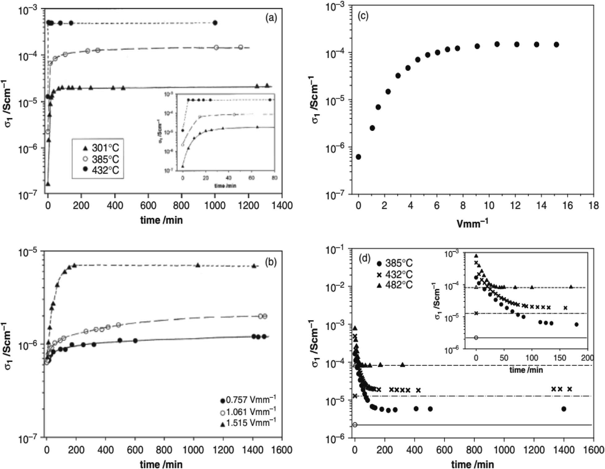 | ||
| Fig. 2 Bulk conductivity of BaTi0.99O2.98 (a) at different temperatures and times with a voltage of 10 V and field 15.1 V mm−1, (b) at different voltages and times at 335 °C, (c) limiting conductivity for different voltages at 335 °C and (d) recovery at different temperatures on removal of the bias voltage (horizontal lines indicate the initial conductivity before voltage application); reproduced from H. Beltran et al., J. Am. Ceram. Soc., 2011, 94, 2951 with permission from Wiley publishing. | ||
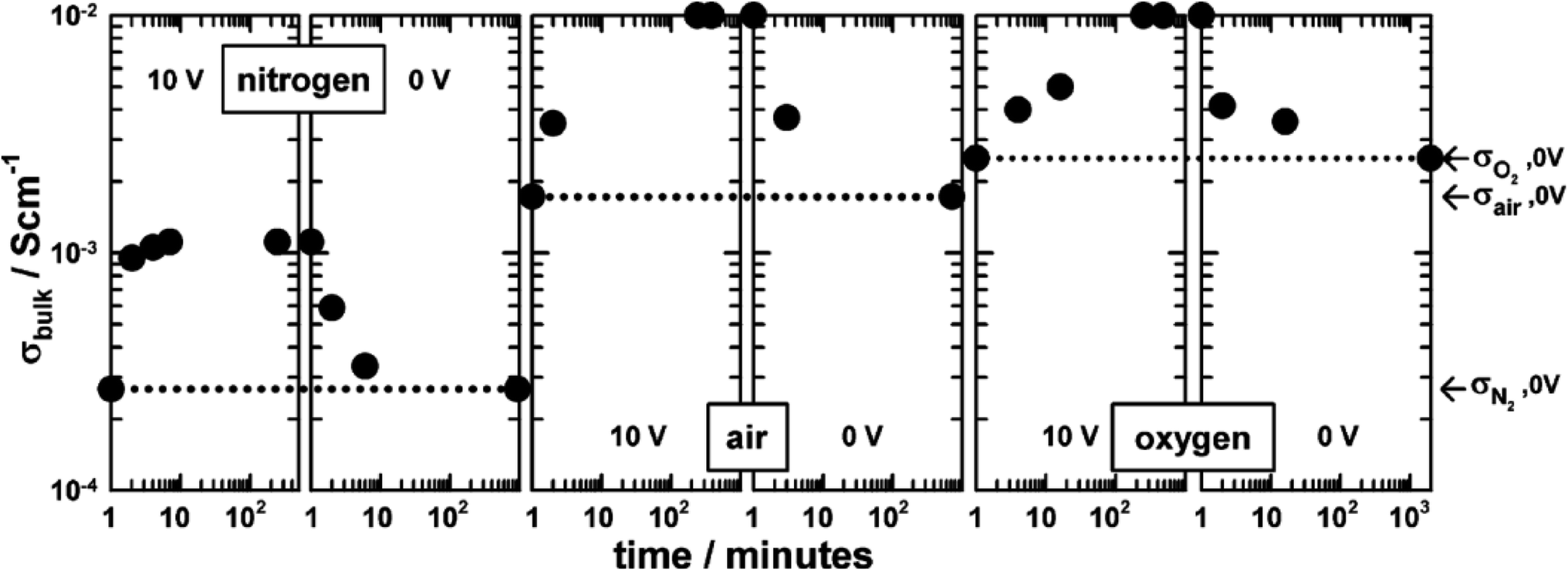
The combined effects of pO2 and voltage together are shown for pellets of BaTi0.99Ca0.01O2.99 in Fig. 3.5 Without an applied bias, the conductivity increases in the sequence N2, air and O2, consistent with an increase in p-type conductivity. In each atmosphere, on application of a voltage the conductivity increases further, and reversibly, by at least one order of magnitude, as shown for application of 10 V at 600 °C. Although the conductivities are pO2-sensitive with 0 V bias, and increase by 1–2 orders of magnitude with an applied bias, oxygen exchange between atmosphere and samples appeared not to occur with voltage application, as confirmed by similar studies on Mg-doped BaTiO3.3 Experiments with a sample under vacuum showed similar conductivity changes to those in air, on both application and removal of voltage, 166.7 V cm−1 at 274 °C. This therefore excluded the possibility of significant gas–solid interactions during application and removal of the voltage in these particular doped BaTiO3 samples.
 | ||
| Fig. 3 Bulk conductivity of BaTi0.99Ca0.01O2.99 with 10 V bias in different atmospheres at 600 °C; reproduced from N. Maso et al., Appl. Phys. Lett., 2010, 97, 062907 with permission from AIP publishing. | ||
Various systematic studies such as these on a range of materials have led to several significant conclusions:
(i) The presence of under-bonded oxide ions in acceptor-doped materials greatly facilitate hole formation and p-type conductivity. This was shown by a lack of voltage sensitivity in stoichiometric BaTiO3, in contrast to the high sensitivity of undoped, but non-stoichiometric BaTiO3 that had either Ba or Ti vacancies:6 these vacancies can be regarded as zero valence cation acceptor dopants and give rise to under-bonding of surrounding oxide ions. Studies of the electrical properties of the classic oxide ion conductor yttria-stabilised zirconia, YSZ were carried out to test the hypothesis that Y3+, as an acceptor dopant in YSZ, should lead to under-bonded oxide ions as well as the oxygen vacancies expected for charge compensation. Results confirmed the hypothesis and showed that oxide ion conducting YSZ with a cubic fluorite structure became a mixed conductor whose level of p-type conductivity increased with increasing voltage,12–15Fig. 4; the effect was accelerated in atmospheres of increasing pO2. Similar results have been obtained in ceramics of the related fluorite structure, yttria-stabilised hafnia, YSH.16,17
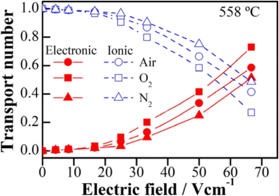 | ||
| Fig. 4 Transport numbers as a function of bias voltage at 558 °C in three different atmospheres; reproduced from X. Vendrell and A. R. West, J. Am. Ceram. Soc., 2019, 102, 6100, with permission from Wiley publishing. | ||
(ii) Although so far, there has been little direct spectroscopic evidence for the presence of O− ions and their effect on voltage- and atmosphere-dependent conductivities, the similarity of results on a wide range of non-transition metal-containing oxides excludes the possibility that stray impurities such as Fe could be responsible for the observed phenomena.
(iii) The generation of p-type conductivity may involve, at least in part, gas–solid exchange of oxygen between samples and the atmosphere. Thus, although results on acceptor-doped BaTiO3 showed similar large increases in p-type conductivity in atmospheres of different pO2, results on YSZ showed greater conductivity increases in atmospheres of increasing pO2.
(iv) Time-dependent, thermally-activated bulk diffusion processes appear to be rate-limiting in the response of samples to changing voltage or pO2. This is shown by the time-dependent effect of temperature on the conductivity changes, Fig. 2 and 3, as well as the time-dependent change in conductivity that occurs on application and removal of a bias voltage.
(v) The voltage-induced conductivity changes in perovskites are not limited to BaTiO3 which is ferroelectric but are also shown by SrTiO3 (ref. 8) and CaTiO3 (ref. 7) which are not. Ferroelectric phenomena are not an essential component, therefore.
(vi) The particular materials studied so far that show enhanced p-type conductivity did not decompose although the applied voltages were well above any theoretical decomposition voltage. They therefore entered a region of kinetic stability but thermodynamic metastability. The changes observed were fully reversible on removing the voltage.
The electronically conducting component of the various perovskite and fluorite materials discussed above is p-type at small applied voltages, but several examples have been found of a switch to n-type conductivity at higher voltages. This is illustrated for an yttria-rich YSZ composition, Y0.5Zr0.49Mg0.01O1.74 in Fig. 5. Data are shown at 800 °C for the change in total resistance with increasing voltage in three atmospheres of different pO2.13,14 Resistance decreases slightly with voltage in the p-type region in all three atmospheres but a marked discontinuity and more rapid rate of decrease occurs above 2 V in N2, above 8 V in air and above 10 V in O2. Separate tests showed that the discontinuities were associated with a change from p-type to n-type as the dominant conduction mechanism. These results give insights into the mechanisms responsible for field-induced conductivity changes, as illustrated in Fig. 6.14 Two sets of mechanisms are identified, at low and higher voltages, which correspond essentially to the two regions on either side of the discontinuities in Fig. 5.
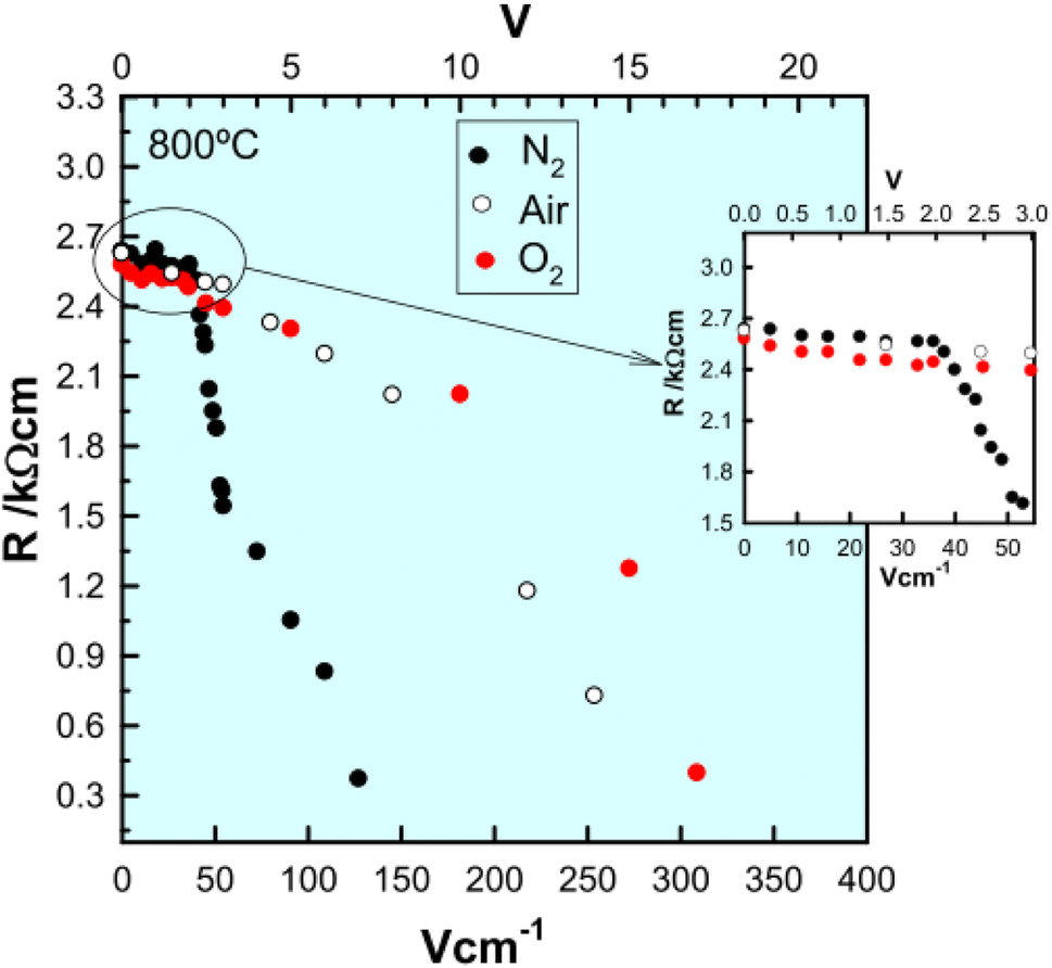 | ||
| Fig. 5 Resistance of Y0.5Zr0.49Mg0.01O1.74 as a function of bias voltage at 800 °C in different atmospheres; reproduced from M. Jovani et al., Sci. Rep., 2019, 9, 18538, with permission from Springer Nature. | ||
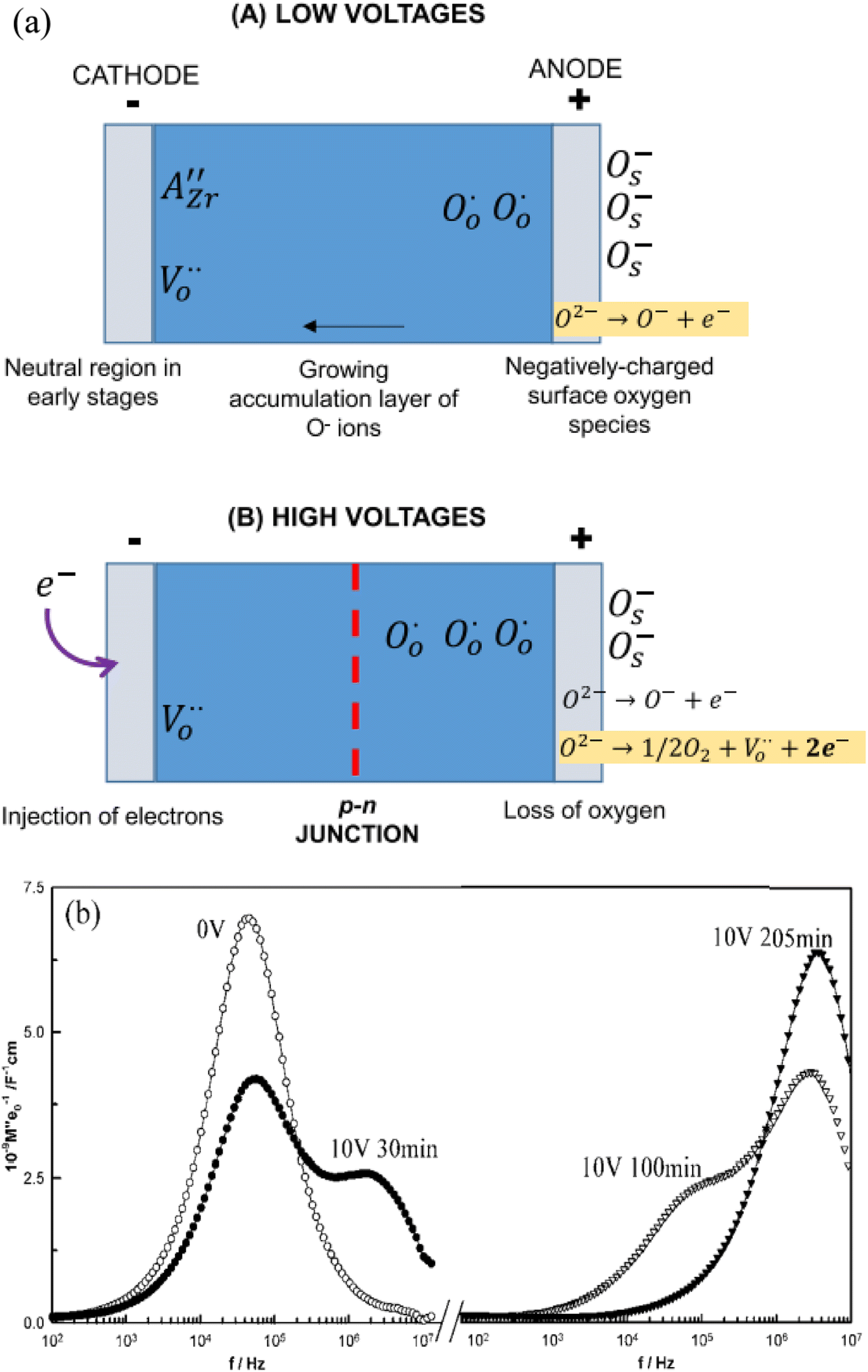 | ||
| Fig. 6 (a) Model for voltage-dependent resistance at low and higher voltages; reproduced from M. Jovani et al., Sci. Rep., 2019, 9, 18538 with permission from Springer Nature; (b) M′′ spectra showing evolution with time of the electrical microstructure of BaTi0.99Mg0.01O2.99 ceramic with a bias voltage of 10 V at 242 °C; reproduced from M. Prades et al., J. Mater. Chem., 2010, 20, 5335 with permission from the Royal Society of Chemistry. | ||
At relatively low voltages, Fig. 6(a) (A), under-bonded O2− ions in the region of the positive electrode undergo single ionisation, eqn (5), leaving holes on those oxygens. The liberated electrons are either trapped at the anode-sample interface, similar to charge storage on the plates of a capacitor, or react with O2 molecules adsorbed from the atmosphere, reverse of eqn (6). A surface layer of p-type conductivity forms at the anode interface and extends into the interior with increasing time under bias.
Evidence of this growth process was obtained from impedance results on composition BaTi0.99Mg0.01O2.99 in which a second, more conductive bulk component was seen which grew thicker with time under bias,3Fig. 6(b). For this, the impedance data were analysed using the electric modulus, M′′, formalism which shows peaks at different frequencies that correspond to the main impedance components of a sample and in which, peak height correlates approximately with volume fraction of that component. In the original, zero-bias sample, a single M′′ peak is observed, consistent with an electrically homogeneous sample. After a few minutes, a second component with higher conductivity appears at higher frequency, which grows with time until, after 205 min only the high conductivity component was seen. This was attributed to formation of an accumulation layer of O− ions at the anode whose conductivity is higher than that of the zero bias sample.3,4
The possibility of hole injection at the anode is not new and was reported in early results on single crystals of BaTiO3 and SrTiO3.22,23 Gold electrodes were used and, similar to Fig. 2 and 3, a time-dependent increase in conductivity was observed, but under slightly different conditions, 130 °C with a field of 1 kV cm−1. At that time, no suggestions were made concerning the location of the holes.
The hole concentration and therefore, magnitude of the hole conductivity depends on both voltage and temperature, as shown in Fig. 2; with time, a steady state conductivity is achieved and presumably corresponds to the point at which the p-type region has expanded to cover the whole sample. The number of O− ions responsible is not known and is likely to be small but nevertheless, is sufficient to control the level of electronic conductivity, especially in ionic titanate perovskites which, in the absence of a bias voltage, are insulating. At low voltages, significant changes at the cation-sample interface are not in evidence and are not needed to explain the observed results.
At higher voltages, (B), an additional process involving either double ionisation of O2− ions, eqn (4), or ionisation of O− ions, eqn (6) occurs. O2 molecules are liberated at the anode and the liberated electrons are re-injected at the cathode. With time, the n-type donor layer that forms at the cathode thickens as it grows inwards from the cathode interface. Since the number of liberated electrons is likely to exceed the hole concentration, samples exhibit overall n-type conductivity when the n-type layer covers the whole sample. The amount of oxygen loss, and the associated increase in conductivity, increases with increasing voltage, as shown in Fig. 5. It can be suppressed in atmospheres of increasing pO2 as shown by the shift in voltage required to see the p- to n-crossover in Fig. 5.
It is clear that separate regions of p- and n-type behaviour can be induced in these oxide materials, commencing at the positive and negative electrode interfaces, respectively. With increased time, the n- and p-regions extend into the sample interior. This gives rise to two possible outcomes. Either one or other region expands across the whole sample and dominates the sample conductivity; under appropriate circumstances, evidence for both of these has been seen. Or, they meet at a p–n junction. There is a clear link between the possibility of p–n junction formation and luminescence phenomena associated with the recently-discovered process of flash sintering, FS.24
In FS experimentation, a voltage of typically 100 V is applied across a solid sample of an oxide such as YSZ, which can be in the form of a powder compact, ceramic or even a single crystal. Starting from a temperature of typically 900 °C, the temperature is gradually increased and three phenomena are observed: the conductivity of the sample starts to increase slowly followed by a sudden jump; at the same time, a pellet compact densifies rapidly within a few seconds and the sample luminesces. Many studies of FS have been reported in the previous one to two decades and the detailed mechanisms are still not well-understood, in particular whether the luminescence is thermo- or electro-in origin. In some cases, samples show an abrupt temperature rise attributed to Joule heating and the possibility of thermoluminescence. In other cases, the temperature rise appears to be modest and the luminescence may be associated with electron–hole recombination, such as could occur as current flows across a p–n junction.
A similar conclusion regarding the creation of both p- and n-type regions in the same sample was reached in the early study on single crystal BaTiO3 and described as ‘double space charge injection in solids’.22
The above examples are of perovskite- and fluorite-structured materials that, without an applied bias, are electronically insulating at ambient temperatures. With small bias, they exhibit p-type conductivity and some examples are known in which n-type conductivity becomes dominant at higher voltages. Any oxide ion conductivity becomes significant only at high temperatures, above about 300 °C. In contrast to these materials and results, more dramatic increases in conductivity at temperatures just above room temperature were observed in perovskite-structured Ca-doped BiFeO3, BCF, Fig. 7.9,10 This material is a good oxide ion conductor associated with charge-compensated vacancies generated on replacing Bi3+ by Ca2+. It is semiconducting due to the presence of Fe and the possibility of mixed valence Fe with mixing of O 2p and Fe 3d orbitals in the band structure. With increasing applied field, the level of p-type conductivity increases rapidly, leading to a reversible transition to a highly conducting state with itinerant electrons, Fig. 7 and 8. This was the first reported example of field-induced, resistive switching in a bulk ceramic,13 together with a more recent example in yttria-stabilised hafnia, YSH, Hf0.85Y0.15O1.925,16,17Fig. 9.
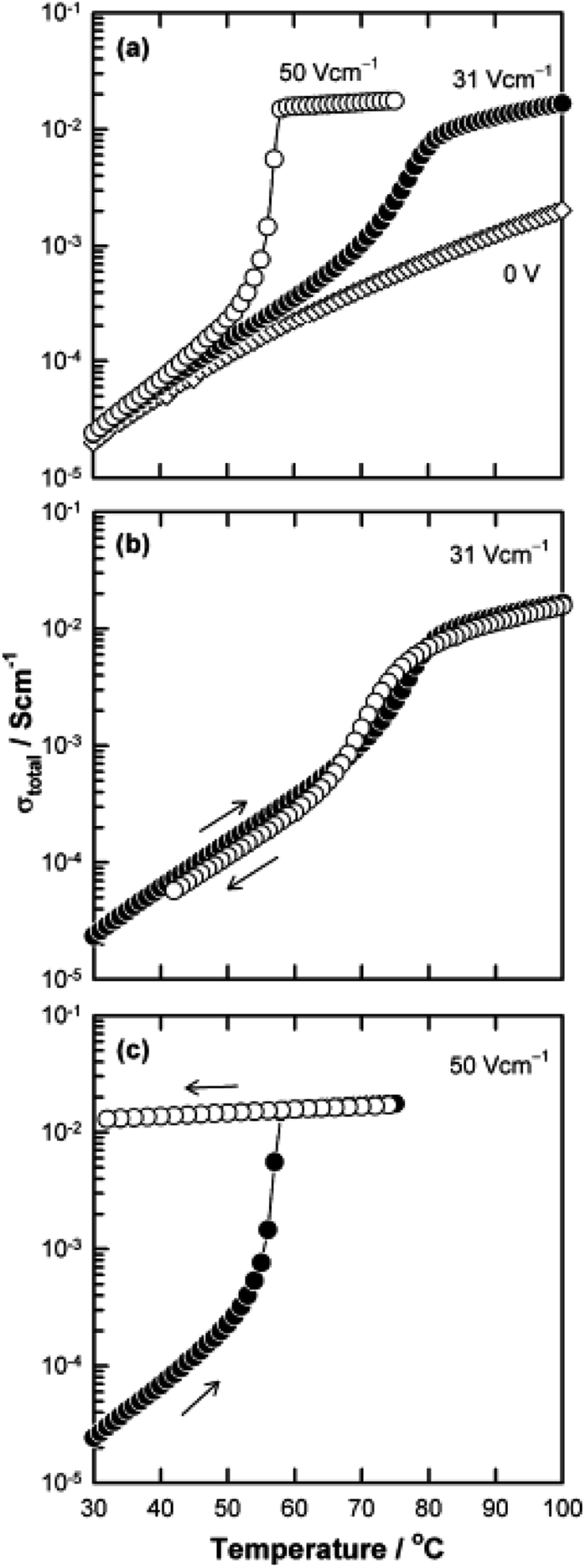 | ||
| Fig. 7 Bulk conductivity of Bi0.95Ca0.05FeO3 against temperature without and with applied fields of 31 and 50 V cm−1; reproduced from N. Maso et al., Phys. Chem. Chem. Phys., 2014, 16, 19408 with permission from the PCCP owner societies. | ||
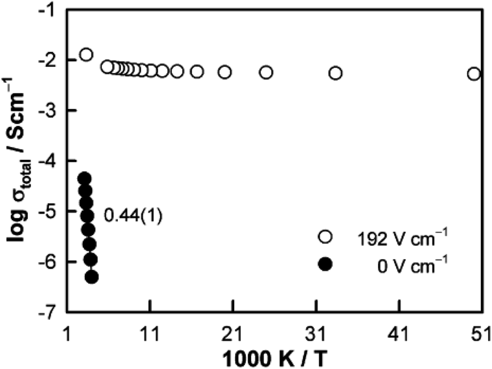 | ||
| Fig. 8 Arrhenius plots of the total conductivity of Bi0.95Ca0.05FeO3 measured without a dc bias and with an applied field of 192 V cm−1; reproduced from N. Maso et al., Phys. Chem. Chem. Phys., 2014, 16, 19408 with permission from the PCCP owner societies. | ||
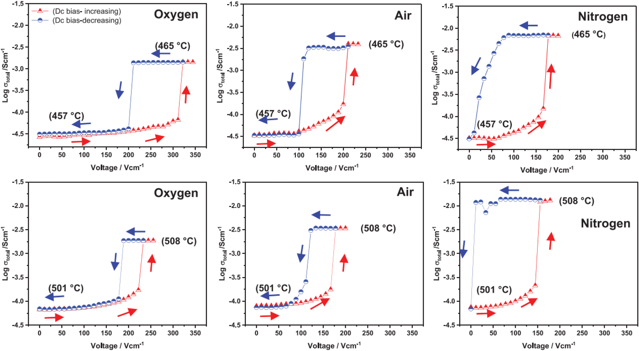 | ||
| Fig. 9 Total conductivity at two temperatures and in atmospheres of different pO2 of Hf0.85Y0.15O1.925 on a stepwise cycle of increasing and decreasing applied voltage after reaching a steady state at each voltage; reproduced from ref. 12: M. Alotaibi et al., J. Am. Ceram. Soc., 2023, 106, 822 with permission from Wiley publishing. | ||
The resistive switching results in Fig. 7–9 show an abrupt, voltage-induced change in conductivity by 2–3 orders of magnitude in two materials, BCF and YSH. If we describe this as an OFF-On transition, it has the following characteristics. The conductivity in the ON state shows very little temperature-dependence; it is the same at 20 K and room temperature, Fig. 8, with the implication that the mobile carriers are delocalised in an energy band. The conductivity in the ON state shows very little voltage dependence, Fig. 9, but increases to a new steady state value with decreasing pO2. The implications are that oxygen equilibria between sample and atmosphere, and therefore the electronic carrier concentration, eqn (7), are influenced by the voltage. The conductivity increases with decreasing pO2 and therefore appears to be n-type in the ON state. The OFF-ON transition is either sharp above a certain voltage or spread over a range of temperatures at lower voltage, as shown in Fig. 7(a) for fields of 0, 31 and 50 V cm−1.
2.2. Resistive switching, metal-insulator transitions and memristors
The resistive switching shown in Fig. 7 and 9 does not involve a crystallographic phase transition as the materials have cubic perovskite and fluorite structures. However, step changes in electrical conductivity of materials are often associated with phase transitions between different crystal structure polymorphs such as the Verwey transition in magnetite, Fe3O4 (ref. 25) and the metal-insulator, MI, transition in VO2.26,35 These typically involve changes in the interatomic distances between transition metal cations and/or a change from electron localisation in metal atom pairs in the low conductivity polymorph to a delocalised band structure in the highly conducting polymorph. In such cases, resistive switching occurs in response to change of temperature and is usually reversible. Many different origins of MI transition have been identified, such as compositionally-driven in the cuprate superconductors.36The resistive switching shown here is also different from that in memristors which are thin film devices. Their ON-OFF switching involves the forming and breaking of conductive filaments through nanometre-thick films of numerous materials, which are usually, but not always, oxides.27 Switching involves application of an external voltage which is small, typically 1–2 V, but must involve high field gradients. A preforming stage is necessary and involves application of a somewhat higher voltage after which, repeated reversible switching is possible. Atomic displacements appear to be involved in both preforming and switching and may be associated with oxygen vacancies or Ag atoms, although the conductive filaments and the switching mechanism must presumably be electronic. Various mechanisms of memristive action have been proposed and are not reviewed here.
Like memristors, switching in BCF and YSH is voltage-induced, but the sample thicknesses are several orders of magnitude greater than those in memristors and therefore, much smaller field gradients are involved. Data for YSH are shown in Fig. 9 at two temperatures, 465 and 508 °C and in three atmospheres of different pO2.17 All six data sets have a similar profile but systematic differences are characterised by: (i) reversible switching, with hysteresis, on voltage cycling, (ii) the ON state conductivity that increases with decreasing pO2 at both temperatures, (iii) OFF-ON and ON-OFF switching temperatures that decrease with decreasing pO2.
The switching results shown in Fig. 7–9 are different in character and origin from both memristive switching and metal-insulator phase transitions but also show some similarities. There are no crystallographic phase changes at temperatures in the vicinity nor is there any suggestion of a voltage-induced crystallographic transition, in spite of the reversibility of the changes to electrical properties. Carrier concentration appears to be a critical, temperature-dependent parameter and above a certain concentration, the charge carriers occupy a delocalised energy band. Using polaron terminology,37–39 the carriers become large polarons distributed over a large number of atoms. In the OFF state, the carriers may be small polarons, localised on specific atoms, most probably oxygen. For the data shown in Fig. 7(b), the polaron size would increase over a range of temperatures and attain the full ON state at somewhat higher temperature. This carrier concentration-dependent behaviour may also be regarded as a sensitive and tunable example of a Mott transition.28
3. Anion redox in Li, Na batteries
In the past 20 years, following the work of Thackray and others,29,30 it has been realised that oxygen redox activity is a common feature of high capacity lithium battery cathodes simply because, as a first observation, experimental charge and discharge capacities are too high to be explained by redox activity of the transition metal cations present alone. On application of high voltages during charge, especially above 4 V, oxygen gas is often liberated consistent with double ionisation of oxide ions, eqn (4). The oxygen loss on charging is then usually irreversible, although there is evidence that it may sometimes be trapped in pores of the cathode structure and, therefore available on subsequent discharge.31The unexpectedly high capacities may be attributed to the single ionisation of oxide ions giving O− ions as part of a reversible O2−/O− redox couple. This is in addition to the usual redox activity of the transition metal components of the cathodes. There is now a very extensive literature on this topic in both Li and Na cathodes, which is not reviewed here. Nevertheless, some observations may be made. First, the cathodes may already have significant electronic conductivity due to the transition metals present; consequently, the resulting electronic structure may be more band-like than ionic, making it difficult to assign capacities to specific redox active species amongst the cations and/or oxygen. Second, the nature of the oxygen species in charged cathodes is unclear and frequently, authors refer to the involvement of catenated oxygen species such as peroxide ions, O22− and other small polymeric anions. Here, for convenience and in the absence of diagnostic experimental data, the possible oxygen species of intermediate valence are referred to as O− ions. Third, arising from the observed redox activity of oxygen in acceptor-doped perovskite and fluorite structures discussed above, acceptor-doping of cathode materials leading to under-bonded, redox-active oxide ions may provide a novel pathway to obtain increased oxygen redox activity and therefore, increased charge capacity.
4. A spectrum of possibilities for emerging phenomena
The various phenomena discussed above start from the assumption that oxygen in oxides has the standard-II oxidation state, simply because the O2− ion, which is spontaneously unstable in the gas phase, is stabilised in crystal lattices by the high lattice energies involved. But, there are now well-established circumstances under which some O2− ions are not stabilised sufficiently in this way and they can ionise, either spontaneously or with reduced ionisation potential, leading to the diverse range of emergent phenomena summarised by the cartoon in Fig. 10.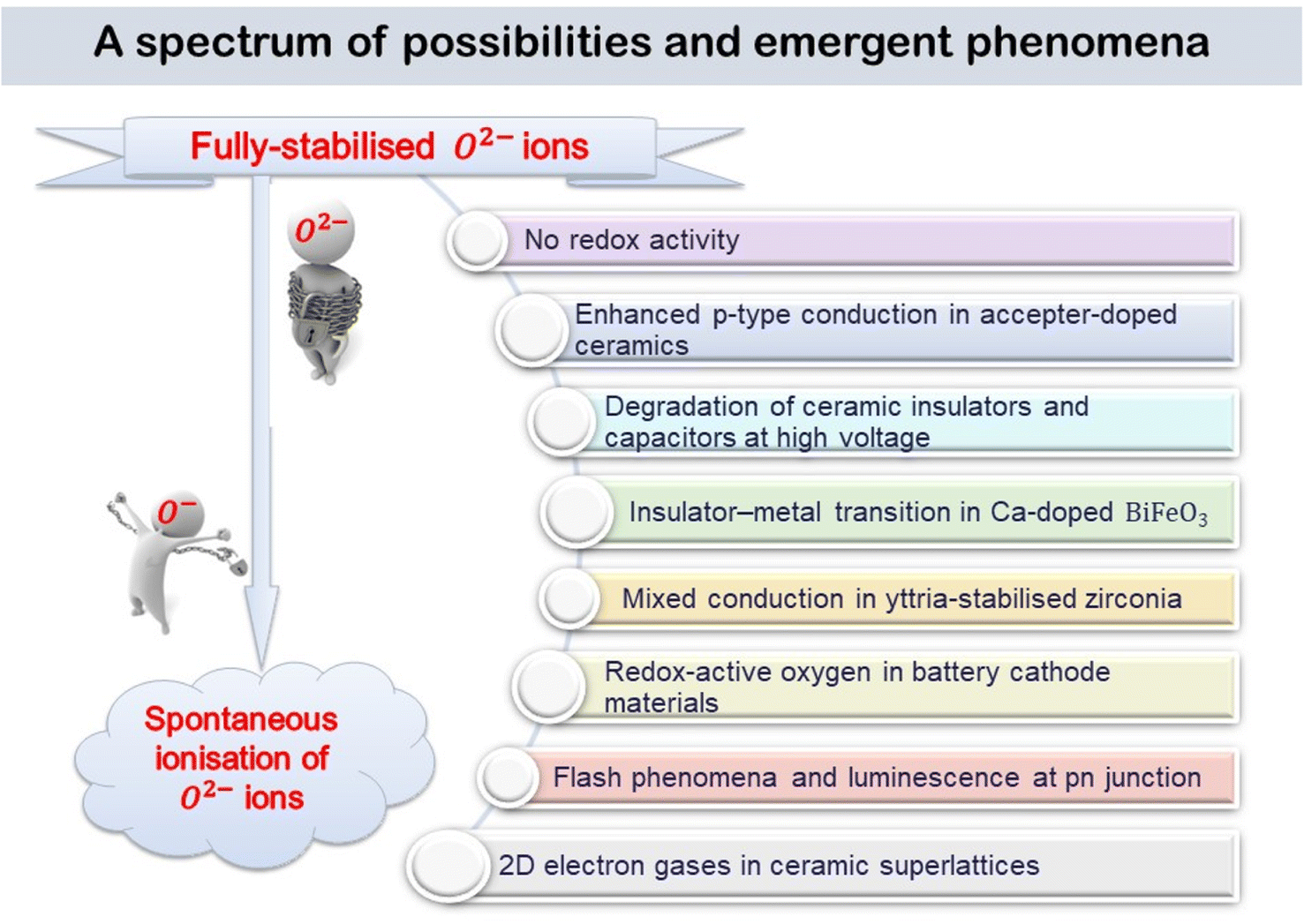 | ||
| Fig. 10 Cartoon showing the range of possibilities and emergent phenomena between the zero conductivity of structures containing fully-stabilised O2− ions and the free electrons in 2D electron gases at layer interfaces of artificial superlattices. | ||
It has been known for many years that electrically-insulating ceramic oxides often exhibit modest levels of p-type semi-conductivity which traditionally, has been attributed to the presence of redox-active Fe impurities that trap holes by effective oxidation of Fe3+ (the common oxidation state of Fe in oxides at high temperatures) to Fe4+. It is now believed that holes can be located on oxygen, as O− ions, and are the main source of p-type conductivity in acceptor-doped titanate perovskites that are insulating when undoped. The O− ions may arise by spontaneous ionisation of under-bonded O2− ions associated with the acceptor dopants, or by redox reaction of those under-bonded oxide ions with O2 molecules from the surrounding atmosphere, as shown by the increasing conductivity with increasing pO2, or by the application of a positive voltage. These processes lead to enhanced p-type conductivity at high temperatures, Fig. 2 and 3 and can by increased further by application of dc voltages in the 20–40 V range. There is a strong similarity between the voltage-enhanced conductivity profile at high temperatures and dielectric breakdown of ceramic insulators which is usually investigated by the application of voltages in the kilovolt range at room temperature.22,23,32,33 Use of temperature as a variable permits the accelerated testing of dielectric breakdown but also provides possible insight into breakdown mechanisms, and possibly a new mechanism, especially in the early stages.
Recognition of the structural features that are responsible for under-bonded oxygen and especially the effect of lower valence acceptor dopants on local electroneutrality, allows the design of materials that have enhanced p-type conductivity in atmospheres of increased pO2 and/or on application of a bias voltage. These can be materials such as alkaline earth titanate perovskites which are electronic insulators when stoichiometric and undoped. Or they can be oxide ion conductors such as acceptor-doped zirconias and hafnias. Depending on the perceived application, the consequences can be either advantageous, such as enhancing the mixed conductivity of materials used as catalysts in solid oxide fuel cell electrodes or disadvantageous, by taking oxide ion conducting solid electrolytes outside their electrolytic domain with the introduction of electronic conductivity that can lead to reduction in fuel cell voltage and the onset of short circuiting.
A quite different application area is in the enhanced capacity of batteries in which the involvement of redox-active oxygen supplements the activity of cathodes associated with mixed valence transition metal components, especially Mn, Ni, Co and Fe. Separation of the contributions of the transition metal and oxygen components is not straightforward, in part because d–p orbital overlap blurs the distinction between anion and cation valences. However, recognition of the effect of acceptor doping on increasing the oxygen redox activity of ionic titanate perovskites does indicate the possible use of acceptor doping as a design strategy to optimise the oxygen contribution to battery cathode performance.
The unexpected discovery of a reversible, insulator-metal transition in Ca-doped BiFeO3 perovskite could be the forerunner of new, emergent phenomena in bulk oxide materials. The effect, recently observed also in fluorite-structured yttria-stabilised hafnia ceramics, is reversible, is not associated with a structural phase transition, but is intimately connected to oxygen redox activity and may involve both ionisation steps, eqn (5) and (6); research into understanding the detailed mechanisms continues.
There is an apparent strong resemblance between the resistive switching in these perovskite and fluorite structures and that involved in memristive switching. The size scales are very different, however, ranging from nm-thick memristor films to mm-thick bulk ceramics. Memristors require an initial ‘forming’ voltage but subsequently show ON-OFF resistive switching on application of a small voltage at room temperature. Several memristive mechanisms have been proposed including unipolar, bipolar and threshold. It will be interesting to see how resistive switching in bulk ceramics and memristors evolves and whether there is any commonality in their switching mechanisms.
The onset, or increase, in p-type conductivity induced by application of a small voltage to acceptor-doped materials, which is attributed to the first step in the ionisation of O2− ions, eqn (5), is superceded at higher voltage in some materials by the creation of n-type conductivity involving either ionisation of O− ions, eqn (6) or double ionisation of lattice O2− ions, eqn (4). Effectively, an applied voltage has different consequences at the two electrodes. It may cause hole injection at the anode and electron injection at the cathode. An increase in time under an applied voltage leads to an increased carrier concentration in the n- and p-type regions but also to their growth from opposite surfaces towards the sample interior. This process presumably commences as a p-i-n configuration but terminates in formation of a p–n junction in the sample interior that may be responsible for the resistive switching and sharp rise in conductivity.
There may also be a close link between these examples of bulk resistive switching and the flash sintering of ceramics, both of which involve sharp increases in conductivity after a premonitory incubation period. The three characteristics of flash sintering: (i) luminescence, (ii) sintering and (iii) conductivity enhancements are not always observed in all samples. Thus, single crystal samples of YSZ are able to flash but do not sinter. If the flash involves electroluminescence rather than thermoluminescence, an electron-hole recombination mechanism is required and may be a consequence of p–n junction creation.
A final, speculative, consequence of the ready ionisation of underbonded oxide ions is the generation of 2-dimensional ‘electron gases’ at the interface between insulating oxide ceramics such as LaAlO3 and SrTiO3. Neither component itself is an electrical conductor and it is often unclear what is the origin of the free electrons in the electron gas, although many studies of the defect structures at the interface have been reported and summarised.34 The explanation may simply be related to the under-bonded oxygens that form the outermost layer of one structure, presumably LaAlO3, which spontaneously ionise, transferring electrons to the other layer, SrTiO3, where they occupy the surface band structure of the Ti 3d orbitals. Local electroneutrality constraints prevent a large separation of the resulting hole and electron layers and the effect is therefore limited to a few atomic layers to either side of the interface.
The experimental observation of 2D electron gases in perovskite layered heterostructures raises interesting general questions as to the extent to which departures from local neutrality can be tolerated. It would also complete the transformation from trapped electrons in fully-stabilised O2− ions to free electrons arising from spontaneous ionisation, as indicated by the cartoon in Fig. 10.
Conflicts of interest
There are no conflicts to declare.References
- L. Pauling, The Nature of the Chemical Bond, Cornell University Press, 3rd edn, 1960 Search PubMed.
- I. D. Brown, Chem. Soc. Rev., 1978, 7, 359 RSC.
- M. Prades, et al. , J. Mater. Chem., 2010, 20, 5335 RSC.
- H. Beltran, et al. , J. Am. Ceram. Soc., 2010, 93, 500 CrossRef CAS.
- N. Maso, et al. , Appl. Phys. Lett., 2010, 91, 062907 CrossRef.
- H. Beltran, et al. , J. Am. Ceram. Soc., 2011, 94, 2951 CrossRef CAS.
- Q.-L. Zhang, et al. , J. Mater. Chem., 2011, 21, 12894 RSC.
- L. G. Escrig, et al. , J. Am. Ceram. Soc., 2014, 97, 2815 CrossRef.
- N. Maso, et al. , Phys. Chem. Chem. Phys., 2014, 16, 19408 RSC.
- N. Maso and A. R. West, Chem. Mater., 2012, 24, 2127 CrossRef CAS.
- M. Guo, et al. , Inorg. Chem., 2018, 57, 64 CrossRef CAS PubMed.
- N. Maso and A. R. West, Chem. Mater., 2015, 27, 1552 CrossRef CAS.
- M. Jovani, et al. , Inorg. Chem., 2017, 57, 7081 CrossRef PubMed.
- M. Jovani, et al. , Sci. Rep., 2019, 9, 18538 CrossRef CAS PubMed.
- X. Vendrell and A. R. West, J. Am. Ceram. Soc., 2019, 102, 6100 CrossRef CAS.
- M. Alotaibi, et al. , Phys. Chem. Chem. Phys., 2021, 23, 25951 RSC.
- M. Alotaibi, et al. , J. Am. Ceram. Soc., 2023, 106, 822 CrossRef CAS.
- J. Ramirez-Gonzalez and A. R. West, Open. Ceram., 2021, 6, 100117 CrossRef CAS.
- D. M. Smyth, The Defect Chemistry of Metal Oxides, Oxford University Press, 2000 Search PubMed.
- P. Ren, et al. , Phys. Chem. Chem. Phys., 2013, 15, 20943 RSC.
- J. Song, et al. , Chem. Soc. Revs., 2020, 49, 2196 RSC.
- G. A. Cox and R. H. Tredgold, Phys. Lett., 1963, 4, 199 CrossRef CAS.
- G. A. Cox and R. H. Tredgold, Br. J. Appl. Phys., 1965, 16, 427 CrossRef CAS.
- M. Cologna, B. Rashkova and R. Raj, J. Am. Ceram. Soc., 2010, 93, 3556 CrossRef CAS.
- F. Walz, J. Phys.: Condens. Matter, 2002, 14, R285 CrossRef CAS.
- M. Imada, Rev. Mod. Phys., 1998, 70, 1039 CrossRef CAS.
- P. Mazumder, et al. , Proc. IEEE, 2012, 100, 1905 Search PubMed.
- N. F. Mott, Rev. Mod. Phys., 1968, 40, 677 CrossRef CAS.
- C. S. Johnson, et al. , Electrochem. Commun., 2004, 6, 1085 CrossRef CAS.
- M. M. Thackeray, et al. , J. Mater. Chem., 2007, 17, 3112 RSC.
- K. McColl, et al. , Nat. Comm., 2022, 13, 5275 CrossRef CAS PubMed.
- S.-H. Yoon, et al. , J. Am. Ceram. Soc., 2009, 92, 1758 CrossRef CAS.
- R. Waser, et al. , J. Am. Ceram. Soc., 1990, 73, 1645 CrossRef CAS.
- Y. Lechaux, et al. , Appl. Phys. Lett., 2022, 121, 081904 CrossRef CAS.
- P. P. Edwards and C. N. R. Rao, Metal-Insulator Transitions Revisited, Taylor and Francis, 1995 Search PubMed.
- Y. Iye, Superconductor-Insulator Transition in Cuprates, 1995, Chapter 11 in ref. 35 Search PubMed.
- Z. Jin, et al. , Light: Sci. Appl., 2022, 11, 209 CrossRef CAS PubMed.
- K. Miyata, et al. , Sci. Adv., 2017, 3, 8 Search PubMed.
- D. Emin, Phys. Rev. B: Condens. Matter Mater. Phys., 1993, 48, 13691 CrossRef CAS PubMed.
| This journal is © The Royal Society of Chemistry 2023 |