
High thermoelectric performance in entropy-driven Ge1−2x−yPbxSnxSbyTe†
Animesh
Das
,
Paribesh
Acharyya
,
Subarna
Das
 and
Kanishka
Biswas
*
and
Kanishka
Biswas
*
New Chemistry Unit and School of Advanced Materials and International Centre for Materials Science, Jawaharlal Nehru Centre for Advanced Scientific Research (JNCASR), Jakkur P.O., Bangalore, 560064, India. E-mail: kanishka@jncasr.ac.in
First published on 24th January 2023
Abstract
Germanium telluride (GeTe) is one of the most fascinating inorganic compounds in thermoelectrics due to its intriguing chemical bonding, crystal and electronic structure. However, thermoelectric performance of pristine GeTe is greatly affected by its high lattice thermal conductivity and intrinsically high p-type carrier concentration. Recently, innovative strategies have been applied to improve thermoelectric performance either by enhancing electronic transport or decreasing the lattice thermal conductivity by phonon scattering. Herein, in order to increase the configurational entropy of the system, we have doped Sn and Pb (2.5 mol% each) in GeTe, which reduces the lattice thermal conductivity (κL) from 2.8 W m−1 K−1 of pristine GeTe to ∼1.9 W m−1 K−1 of Ge0.95Pb0.025Sn0.025Te sample at room temperature. Furthermore, we have doped donor dopant Sb on the Ge site in Ge0.95Pb0.025Sn0.025Te which optimizes the p-type carrier concentration of the system and enhances the Seebeck coefficient due to valence band convergence. Finally, high energy ball-milling along with spark plasma sintering (BM + SPS) has been performed, which helps in further enhancement of the Seebeck coefficient due to extreme valence band convergence and reduction in lattice thermal conductivity to ∼0.63 W m−1 K−1. As a result, a high thermoelectric figure of merit, zT of ∼2.3 (with Dulong–Petit Cp, zT is 2.5) at 723 K and a high average zTavg of 1.3 in the 300–723 K temperature range have been achieved in BM + SPS processed Ge0.84Pb0.025Sn0.025Sb0.11Te sample. Motivated by the ultra-high zT, we have constructed a double-leg TE device of Ge0.84Pb0.025Sn0.025Sb0.11Te (BM + SPS) sample as a p-type leg, where In and I doped PbTe is used as the n-type leg, which shows a high output power density (PDmax) of ∼590 mW cm−2 at ΔT = 448 K.
10th year anniversaryOn the auspicious occasion of the 10th anniversary of Journal of Materials Chemistry A, I would like to take the opportunity to thank as well as congratulate the entire JMC A community for the success of the journal by publishing important articles written by experts in the field. Over the last ten years JMC A has published excellent articles in energy conversion and storage and materials relevant to environmental issues. These have encouraged me to publish in this renowned journal since 2014. Since then, we have published several articles and review papers in this journal such as J. Mater. Chem. A, 2014, 2, 4324; J. Mater. Chem. A, 2015, 3, 648; J. Mater. Chem. A, 2018, 6, 24216; J. Mater. Chem. A, 2018, 6, 13142; J. Mater. Chem. A, 2020, 8, 12226 in the context of thermoelectric energy conversion and water purification. As a future direction of our work, innovating new thermoelectric materials, thermal transport in metal halides and new quantum materials, we will continue to contribute to this journal. I am also acting as an Editorial Advisory Board member in JMC A. |
Introduction
Most of the energy utilization processes generate heat as a byproduct. With two-thirds of used energy lost as waste heat, conversion of such waste heat to a beneficial form can have a significant impact on overall energy utilization.1,2 Thermoelectrics (TE) has become an essential ingredient in green energy technology which converts the waste heat into electrical energy without emitting any hazardous gases like CO and CO2.3,4 The efficiency of a TE solid-state material is governed by the dimensionless figure of merit (zT) defined as zT = σS2T/(κe + κL) where σ, S, κe and κL are the electrical conductivity, Seebeck coefficient, electrical thermal conductivity and lattice thermal conductivity, respectively, at absolute temperature T.5–7 However, σ, S, and κe are interlinked via carrier concentration. Thereby, decoupling electrical and thermal transport properties with the decrease of κL and enhancement of the power factor (σS2) is the most arduous task. Several strategies have already been implemented to enhance the TE performance of a material by increasing the Seebeck coefficient8 and decreasing κL.2 The Seebeck coefficient can be increased via modulation of the electronic structure such as valence band convergence9 resonance level formation etc.,10 whereas, κL has been reduced up to the glass limit by introducing point defect scattering,11 hierarchical nano/meso-scale architectures,12,13 lattice anharmonicity,14 bonding heterogeneities,14–16 liquid-like ion flow,17 ferroelectric instability, etc.18,19In the IV–VI semiconductor family, recently, germanium telluride (GeTe) has emerged as a potential high performance TE candidate due to its unique structure–property relationship.20–23 GeTe crystallizes in a rhombohedral (α phase, R3m) structure (r-GeTe) at room temperature and a rock salt cubic (β phase, Fm![[3 with combining macron]](https://www.rsc.org/images/entities/char_0033_0304.gif) m) structure (c-GeTe) at high temperature (>700 K). It undergoes a paraelectric to ferroelectric structural second-order phase transition from the α phase to β phase at ∼700 K due to the slight displacement of the Ge atoms originating from shear distortion of the lattice along the [111] crystallographic direction. TE properties of pristine GeTe are reasonable and a maximum zT of ∼0.8 is achieved at 723 K limited by its very high p-type carrier density (∼1021 cm−3), originating from intrinsic Ge vacancies. As a consequence, a very high σ of ∼8500 S cm−1, a moderate S of ∼34 μV K−1 and a high κT of ∼8 W m−1 K−1 at 300 K are observed in pristine GeTe.22,24 Nevertheless, over the last couple of years, a large advancement in the TE performance of GeTe has been accounted for by the development of several novel methodologies to modify its electronic structure and phonon scattering mechanisms.20,25,26
m) structure (c-GeTe) at high temperature (>700 K). It undergoes a paraelectric to ferroelectric structural second-order phase transition from the α phase to β phase at ∼700 K due to the slight displacement of the Ge atoms originating from shear distortion of the lattice along the [111] crystallographic direction. TE properties of pristine GeTe are reasonable and a maximum zT of ∼0.8 is achieved at 723 K limited by its very high p-type carrier density (∼1021 cm−3), originating from intrinsic Ge vacancies. As a consequence, a very high σ of ∼8500 S cm−1, a moderate S of ∼34 μV K−1 and a high κT of ∼8 W m−1 K−1 at 300 K are observed in pristine GeTe.22,24 Nevertheless, over the last couple of years, a large advancement in the TE performance of GeTe has been accounted for by the development of several novel methodologies to modify its electronic structure and phonon scattering mechanisms.20,25,26
Recently, configurational entropy engineering has steadily been engendered as a new strategy that synchronizes the carrier concentration optimization of a material with low phonon transport via selective multi-principal-element alloying, and it reveals great prospects for developing new high performance TE materials.11,27–30 Configurational entropy, in a given system, increases with increasing the elemental dopants, thereby decreasing the Gibbs free energy, which facilitates the entropy-driven structural stability along with extending solid solubility limits of the alloying elements.3,31–34 Generally, in the binary systems, as the enthalpy factor exceeds entropy,26 phase separation can easily occur. As a consequence, the defects/dislocations present in the boundary between the phase separated precipitate and matrix scatter the majority charge carriers along with phonons, manifesting a detrimental effect on thermoelectric properties. Such phenomena have also been observed for a few pseudoternary based systems like PbTe1−2xSexSx,35 SnTe1−2xSexSx,30 GeTe1−2xSexSx,11 and Ge1−2xSn2xTe1−2xSexSx.29 However, in case of additional components doping, for example, in a system like Ge0.61Ag0.11Sb0.13Pb0.12Bi0.01Te,27 the entropy of mixing exceeds enthalpy, thus the individual solubility limit of the dopants increases. On the other hand, the formation of point defects and generated local lattice distortions induced by the lattice strain and mass fluctuations owing to multicomponent doping, remarkably scatter the heat carrying phonons, thereby improving zT of the given system.
Herein, we have demonstrated the excellent thermoelectric performance in ball milled and spark plasma sintered (BM + SPS) Sb doped Ge1−2xPbxSnxTe (x = 0–0.05) samples. We have achieved a high zT of 2.3 (with Dulong–Petit Cp, zT is 2.5) at 723 K and a high average zTavg of 1.3 in the 300–723 K temperature range in 11 mol% Sb doped Ge0.95Pb0.025Sn0.025Te (BM + SPS). Exclusive cation site alloying on the Ge position of GeTe using Pb and Sn (2.5 mol% each) and Sb (11 mol%) increases the configurational entropy of the system. SnTe and PbTe both exhibit a cubic rock salt structure at room temperature20,36 and act as a donor dopant to GeTe, which facilitates optimizing the p-type carrier density in GeTe. Furthermore, Sb alloying in Ge0.95Pb0.025Sn0.025Te causes an enhancement in the Seebeck coefficient and decreases the κL value due to extensive valence band convergence and enhanced phonon scattering, respectively. Additionally, high energy ball-milling along with spark plasma sintering results in excessive cationic disorder and formation of Ge nanoprecipitates of sizes ∼10–40 nm in the GeTe matrix, causing a significant reduction in κL to ∼0.63 W m−1 K−1 at room temperature. Furthermore, motivated by the ultra-high zT, a double leg TE device based on the Ge0.84Pb0.025Sn0.025Sb0.11Te (BM + SPS) sample as the p-type leg, where In and I doped PbTe is used as the n-type leg, is fabricated and a promising output power density of ∼590 mW cm−2 for ΔT ∼448 K is achieved.
Results and discussion
We have synthesized high-quality polycrystalline samples of GeTe and Ge1−2xPbxSnxTe (x = 0–0.05) by the vacuum seal tube melting reaction followed by ball milling and spark plasma sintering (see Method in the ESI† for details). Configurational entropy (ΔS) of a solid solution having n number of components with a mole fraction of xi, is defined using the eqn. .3 In the present GeTe-based system, ΔS increases predictably as the number of alloying elements increases as shown in Fig. S1 ESI.† For example, ΔS gradually increases to 1.91 J mol−1 K−1 in Ge0.95Pb0.025Sn0.025Te and further reaches to 2.57 Jmol−1 K−1 in the Ge0.9Pb0.05Sn0.05Te sample. Fig. 1a shows the room temperature PXRD pattern of Ge1−2xPbxSnxTe (x = 0–0.05) samples which could be indexed based on the rhombohedral phase of GeTe and above x ≥ 0.015 we observe a weak diffraction peak of Ge which is characteristic for GeTe based samples.37 With an increase in the Sn and Pb concentrations from 1.5 to 5 mol%, Bragg peaks of pristine GeTe shift to a lower angle (Fig. S2a ESI†) consistent with the increase in the lattice parameter (Fig. S2b and S3 ESI†) of the solid solutions as the sizes of Sn (118 pm) and Pb (119 pm) are larger than that of Ge (87 pm).
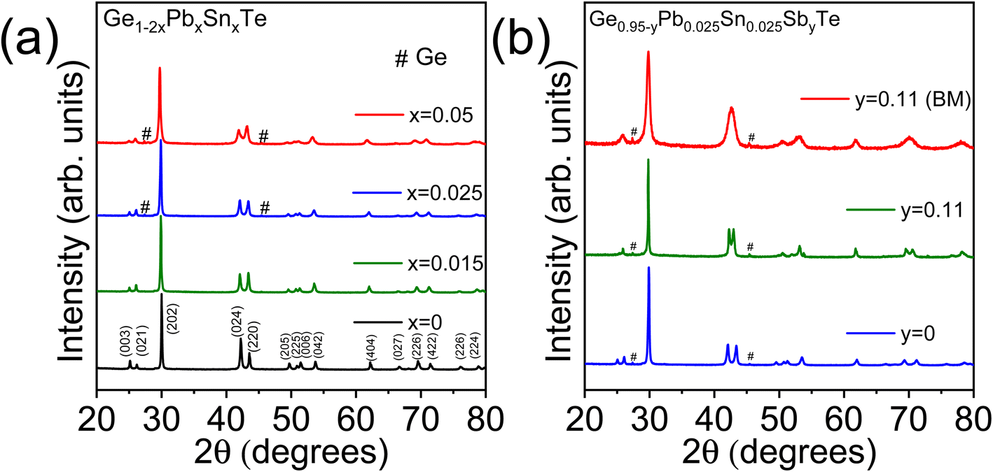 | ||
| Fig. 1 Powder X-ray diffraction of (a) Ge1−2xPbxSnxTe (x = 0–0.05), and (b) ingot and ball milled Ge0.84Pb0.025Sn0.025Sb0.11Te samples. | ||
To probe the microstructure composition, field emission scanning electron microscopy (FESEM) in backscattered imaging (BSE) mode and energy dispersive spectroscopy (EDS) are performed on the polished surface of the Ge0.95Pb0.025Sn0.025Te sample. Fig. 2a and b present different magnified BSE-FESEM images of the polished surface of the Ge0.95Pb0.025Sn0.025Te sample, where we can observe the microprecipitate of Ge of 2–20 μm size in the GeTe matrix, which is further verified by EDS color mapping (Fig. S5 and S6 ESI†) and EDS line spectra along the precipitate (Fig. 2c). Formation of the Ge microprecipitate is typical in GeTe as it has an intrinsic Ge vacancy.20,21,25 To check the nanoscale architecture, high resolution transmission electron microscopy (HRTEM) is performed on the Ge0.95Pb0.025Sn0.025Te sample as shown in Fig. S7 ESI,† where we have not found any nanoprecipitate, indicating that the system forms a high entropy solid solution in Ge1−2xPbxSnxTe, enriched with point defects due to mass fluctuation of cation sites.
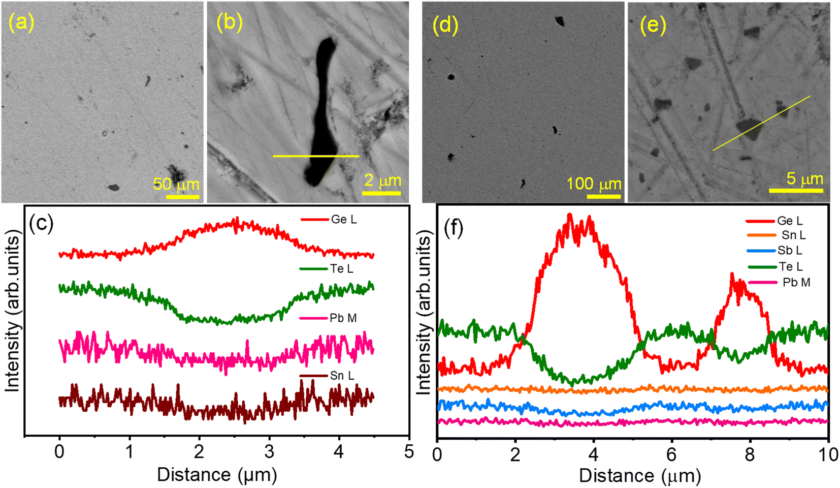 | ||
| Fig. 2 (a and b) Backscattered FESEM images at different magnifications of the Ge0.95Pb0.025Sn0.025Te sample, (c) EDS line scanning along the precipitate as highlighted in (b), (d and e) Backscattered FESEM images at different magnifications of the BM + SPS processed Ge0.84Pb0.025Sn0.025Sb0.11Te sample, and (f) EDS line scanning along the precipitate as highlighted in (e). | ||
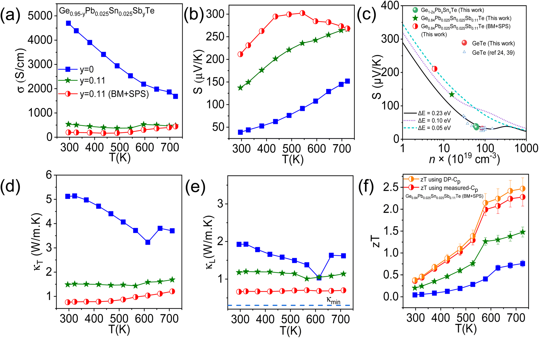
Temperature dependent TE properties of ingot Ge1−2xPbxSnxTe (x = 0–0.05) samples are shown in Fig. 3. Fig. 3a shows the temperature dependent electrical conductivity (σ) of ingot samples, where the decreasing nature of σ with temperature resembles the degenerate semiconductor behavior. With increasing concentrations of Sn and Pb in GeTe, σ decreases. Typically, pristine GeTe exhibits an electrical conductivity of ∼8062 S cm−1 at room temperature, which reduces to 4698 S cm−1 in the Ge0.95Pb0.025Sn0.025Te sample. This can be attributed mainly to a decrease in carrier mobility and carrier concentration, which is verified by room temperature Hall measurement (Table S1 ESI†). The Positive Hall coefficient and positive Seebeck coefficient indicate that the major carrier is the hole. The p-type carrier concentration slightly decreases with the addition of Pb and Sn in GeTe (Table S1 ESI†). The Seebeck coefficient of all the compositions remains similar. Pristine GeTe shows the Seebeck coefficient of ∼31 μV K−1 at room temperature, whereas ingot Ge0.95Pb0.025Sn0.025Te exhibits a S of ∼39 μV K−1 at room temperature and it increases to ∼152 μV K−1 at 723 K (Fig. 3b).
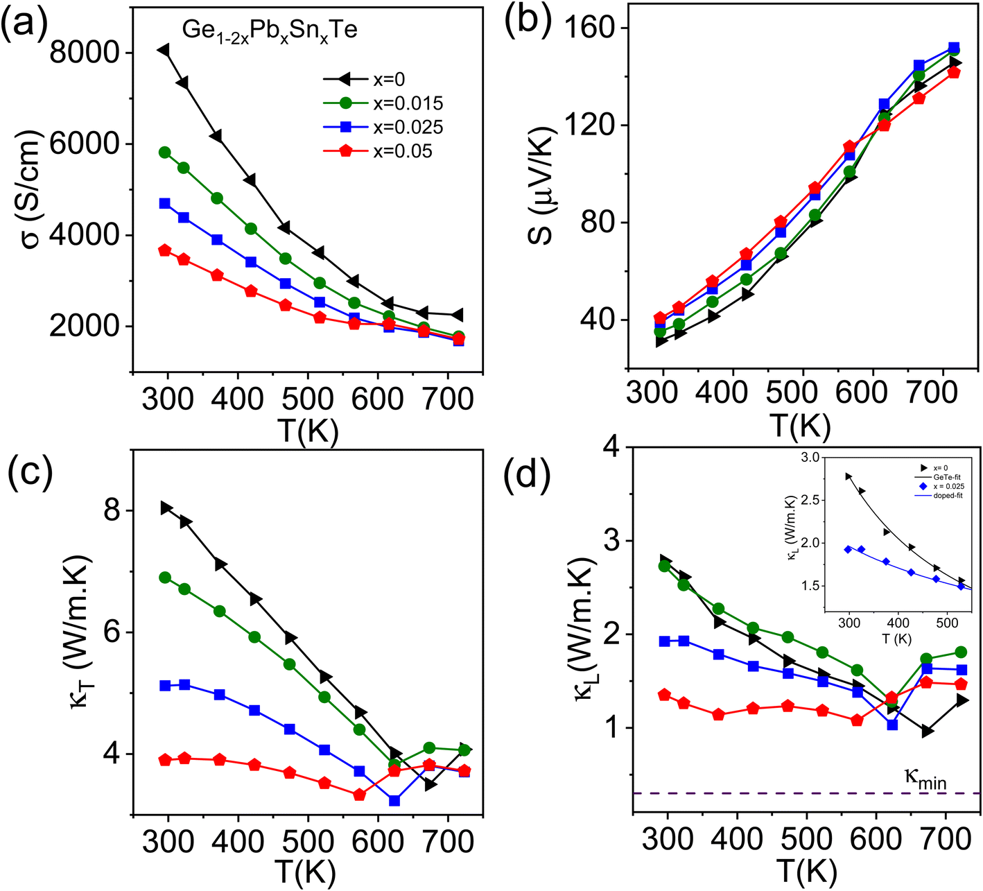 | ||
| Fig. 3 Temperature dependent (a) electrical conductivity (σ), (b) Seebeck coefficient (S), (c) total thermal conductivity (κT), and (d) lattice thermal conductivity (κL) of Ge1−2xPbxSnxTe (x = 0–0.05) samples. The inset of figure (d) shows Callaway's model fitting of κL for pristine GeTe and Ge0.95Pb0.025Sn0.025Te samples. | ||
Temperature dependent thermal transport property data of Ge1−2xPbxSnxTe (x = 0–0.05) samples are illustrated in Fig. 3c and d. Total thermal conductivity (κT) decreases with an increase in Sn and Pb content in GeTe. For example, pristine GeTe shows a κT of ∼8 W m−1 K−1, whereas, for Ge0.95Pb0.025Sn0.025Te, it decreases to ∼5.1 W m−1 K−1 at room temperature. The lattice thermal conductivity (κL) is estimated by subtracting electrical thermal conductivity (κe) from total thermal conductivity (κT). κe is determined by using the equation κe = LσT, known as Wiedemann–Franz's law, where L is the Lorenz number. L of all the Ge1−2xPbxSnxTe (x = 0–0.05) samples is calculated by fitting of the temperature dependent Seebeck coefficient.12 Pristine GeTe shows a κL of ∼2.8 W m−1 K−1, which decreases to ∼1.9 W m−1 K−1 for Ge0.95Pb0.025Sn0.025Te at room temperature and 1.6 W m−1 K−1 at 723 K. The cause of reduction in κL can mainly be attributed to point defects at the cation site (Ge/Sn/Pb) and large mass fluctuations in the system. We have fitted the temperature dependent κL data with Callaway's model for pristine GeTe and Ge0.95Pb0.025Sn0.025Te samples. Callaway devised a phenomenological model considering scattering at various length scales, which is given by,38
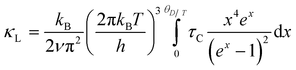
It acts as a guide for quantitative assessment of the contribution arising from different phonon scattering effects. Here, kB corresponds to Boltzmann's constant; h, T and τC denote Planck's constant, absolute temperature and total relaxation time, respectively. τC corresponds to the individual relaxation time obtained via the relation
In the next step, we have further alloyed Sb (11 mol%) on the cation site of the Ge0.95Pb0.025Sn0.025Te sample to optimize the p-type carrier concentration, which eventually, increases the Seebeck coefficient for further improvement in overall TE performance. Overall entropy of mixing (ΔS) also increases considerably from 1.91 J mol−1 K−1 in Ge0.95Pb0.025Sn0.025Te to 4.74 J mol−1 K−1 in the Ge0.84Pb0.025Sn0.025Sb0.11Te sample. Aliovalent Sb(III) doping on the Ge site effectively suppresses the p-type carrier density and also enhances the valence band degeneracy by promoting the crystal symmetry of GeTe to be more cubic in nature at room temperature.13,22,39 Besides, the obtained κL of the Ge0.95Pb0.025Sn0.025Te sample (∼1.9 W m−1 K−1 at 300 K) is much higher than theoretical κmin of pristine GeTe (0.3 W m−1 K−1),40 thus it leaves enormous scope for the further reduction of κL to enhance zT. We have synthesized the Ge0.84Pb0.025Sn0.025Sb0.11Te sample mainly by the solid state melting reaction (synthesis in the ESI†) and recorded the powder XRD pattern at room temperature (Fig. 1b). The two Bragg peaks (024) and (220) which correspond to rhombohedral GeTe, tend to come closer to a single (220) peak of cubic GeTe with a Sb concentration of 11 mol%, indicating the augmented cubic nature in the system.13,22
Temperature dependent electrical conductivity (σ) of the Ge0.84Pb0.025Sn0.025Sb0.11Te sample is shown in Fig. 4a. The σ decreases with Sb doping because of reduction in the p-type carrier density (n) (Table S3 ESI†). Typically, σ reduces from ∼4698 S cm−1 for Ge0.95Pb0.025Sn0.025Te (where n = 6.1 × 1020 cm−3) to ∼540 S cm−1 for the Ge0.84Pb0.025Sn0.025Sb0.11Te (n = 1.5 × 1020 cm−3) sample at room temperature. The variation of the Seebeck coefficient, S, as a function of temperature for the Ge0.84Pb0.025Sn0.025Sb0.11Te sample is unveiled in Fig. 4b. Ingot Ge0.84Pb0.025Sn0.025Sb0.11Te shows a higher Seebeck coefficient than that of the Ge0.95Pb0.025Sn0.025Te sample over the whole temperature range. Typically, the Seebeck value for the Ge0.84Pb0.025Sn0.025Sb0.11Te sample is ∼128 μV K−1 at room temperature which further increases to 230 μV K−1 at 723 K. This increase in the Seebeck coefficient value could be attributed to possible valence band convergence which will be discussed later. The variation of total thermal conductivity (κT) and lattice thermal conductivity (κL) with temperature for the ingot Ge0.84Pb0.025Sn0.025Sb0.11Te sample is shown in Fig. 4d and e. A significant reduction in κT is achieved by 11 mol% Sb doping in Ge0.95Pb0.025Sn0.025Te. The κT value of ingot Ge0.95Pb0.025Sn0.025Te is ∼5.1 W m−1 K−1 which is suppressed to ∼1.4 W m−1 K−1 in Ge0.84Pb0.025Sn0.025Sb0.11Te at room temperature. The κT value shows an anomaly at 573 K of Ge0.95Pb0.025Sn0.025Te, which is due to structural phase transition of GeTe. The lattice thermal conductivity (κL) of the ingot Ge0.84Pb0.025Sn0.025Sb0.11Te sample is obtained by subtracting κe from κT (Fig. 4e). The κe is calculated using the Wiedemann–Franz law, κe = LσT where the Lorenz number (L) is calculated from the temperature dependence of the Seebeck coefficient by fitting the reduced Fermi energy considering the contributions from double valence bands of GeTe.13,36,41 Ingot Ge0.84Pb0.025Sn0.025Sb0.11Te shows a low κL ∼1.1 W m−1 K−1 at room temperature. Sb doping in Ge0.95Pb0.025Sn0.025Te creates more solid solution point defects, thereby reducing the lattice thermal conductivity by enhanced phonon scattering. As there is still room to decrease the lattice thermal conductivity, we did ball milling (BM) followed by SPS on the Ge0.84Pb0.025Sn0.025Sb0.11Te sample.
 | ||
| Fig. 4 Temperature dependent (a) electrical conductivity (σ), (b) Seebeck coefficient (S), (c) Pisarenko plot (S vs. n) at 300 K, (d) total thermal conductivity (κT), (e) lattice thermal conductivity (κL) and the (f) thermoelectric figure of merit (zT) of ingot and (BM + SPS) processed Ge0.84Pb0.025Sn0.025Sb0.11Te samples using measured Cp and Dulong–Petit (DP) Cp. | ||
The room temperature PXRD pattern of the BM Ge0.84Pb0.025Sn0.025Sb0.11Te sample is shown in Fig. 1b. We have observed an apparent merging of (024) and (220) reflections in between 2θ = 41 and 45° along with broadening of the Bragg's reflections. We have done the Rietveld analysis based on PXRD data of ingot and ball milled Ge0.84Pb0.025Sn0.025Sb0.11Te samples as shown in Fig. S4 ESI.† Slight reduction of the c/a ratio in the rhombohedral setting in BM Ge0.84Pb0.025Sn0.025Sb0.11Te compared to that of the ingot sample implies reduction of rhombohedral distortion (Table S5 ESI†). However, peak broadening of the XRD peak is also due to the reduction of the crystallite size (discussed later). Ball milling in the Ge0.84Pb0.025Sn0.025Sb0.11Te sample causes a decrease in rhombohedral distortion, but the reduced crystallite size effect is more pronounced as observed from the XRD reflections and TEM images.
We have performed microscopic analysis to investigate the cause of PXRD peak broadening in the Ge0.84Pb0.025Sn0.025Sb0.11Te (BM) sample. BSE-FESEM of Ge0.84Pb0.025Sn0.025Sb0.11Te (BM + SPS) is performed to analyze the microstructure composition. Fig. 2d and e show the FESEM micrographs at different magnifications. It is found that the Ge microprecipitate (∼5–10 μm size) is present in the matrix, which is further confirmed by color mapping (Fig. S8 ESI†), and EDS line scanning (Fig. 2f) along the precipitate which appears as a dark contrast in Fig. 2e. To probe the nanoscale architecture, TEM and HRTEM analyses of the same sample are carried out. TEM images show that the BM processed Ge0.84Pb0.025Sn0.025Sb0.11Te sample exhibits particle sizes of ∼40–60 nm (Fig. S9a ESI†), which contribute to the peak broadening during X-ray diffraction. HRTEM images in Fig. 5d and S9b ESI† reveal that the d-spacing of the matrix is ∼0.29 nm, which corresponds to the (202) plane of the rhombohedral phase of GeTe (R3m). Furthermore, low magnification TEM images show the presence of nanoprecipitates in the GeTe matrix (Fig. 5a) with a d-spacing of 0.32 nm indicating the (111) plane of Ge (Fdm), and hence confirms the presence of Ge nanoprecipitates (10–40 nm size) in the matrix (Fig. 5b and c). In addition, we have performed the EDS color mapping in the GeTe matrix in STEM-HAADF mode, which further validates the presence of nanosized Ge precipitates in the GeTe matrix as shown in Fig. S10 ESI.† It is noteworthy to mention here that besides the presence of Ge nanoprecipitates, ripple-like nanostructures and dislocations in the GeTe matrix are also observed as shown in Fig. S11 ESI.† This can be attributed to high lattice strain induced in the system due to high energy ball milling, large mass fluctuations and the enhanced cubic nature after Sb doping.42 Existence of such ripple-like nanostructures and dislocations in the matrix is further verified via performing inverse fast Fourier transform (IFFT) (Fig. S11d ESI†) of the area selected in Fig. S11c ESI.†
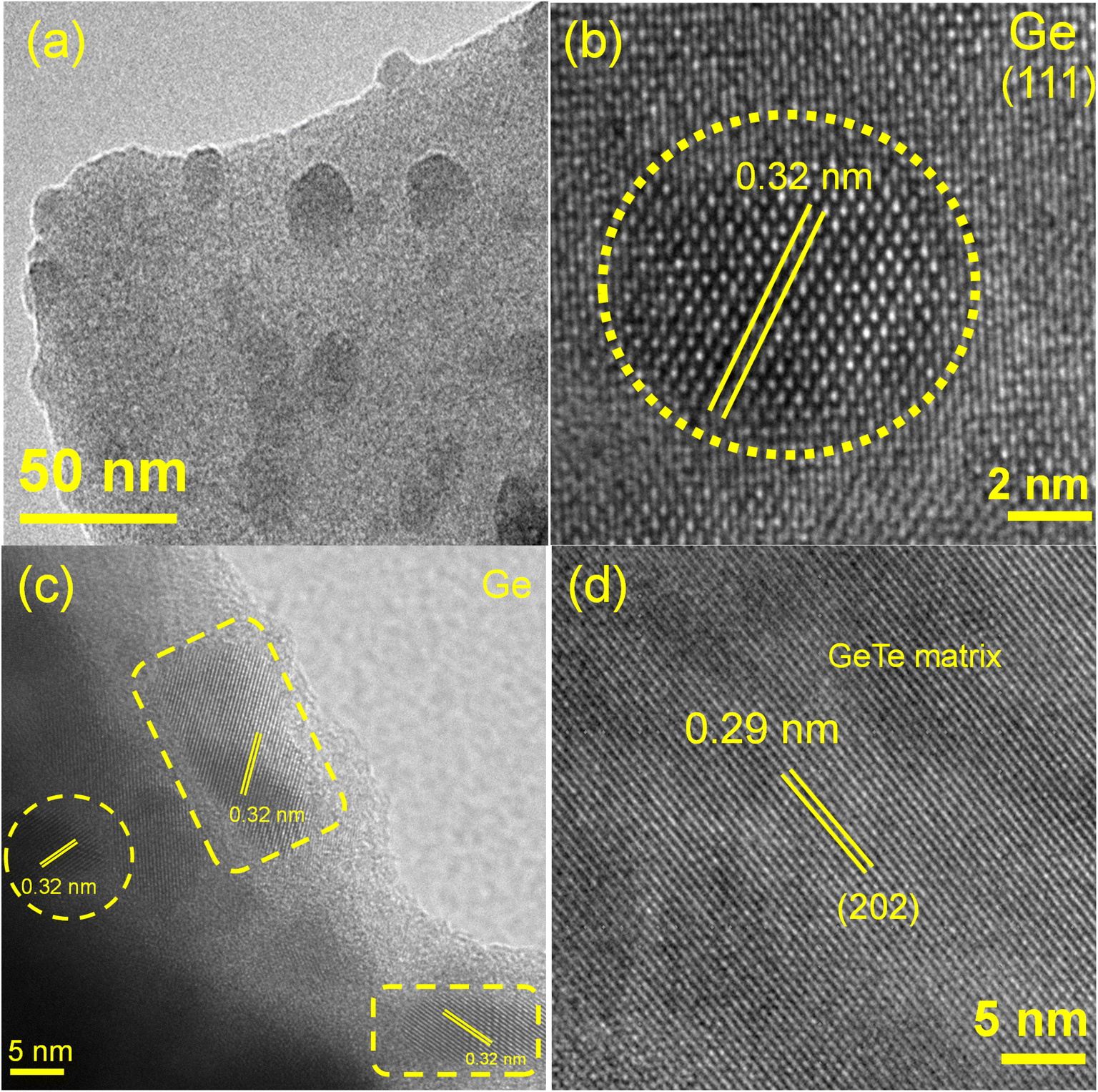 | ||
| Fig. 5 (a) TEM image of the BM + SPS processed Ge0.84Pb0.025Sn0.025Sb0.11Te sample showing the presence of nanoprecipitates in the matrix, (b and c) HRTEM micrograph of the same sample showing the presence of the Ge nanoprecipitate, and the (d) HRTEM image of the GeTe matrix having a d-spacing of 0.29 nm. | ||
Furthermore, we have measured temperature dependent TE properties of the BM + SPS processed Ge0.84Pb0.025Sn0.025Sb0.11Te sample as shown in Fig. 4. In Fig. 4a, electrical conductivity in Ge0.84Pb0.025Sn0.025Sb0.11Te (BM + SPS) decreases drastically because of the significant decrease in carrier concentration (Table S3 ESI†). Ingot Ge0.84Pb0.025Sn0.025Sb0.11Te has a σ of ∼540 S cm−1 at 300 K, whereas it reduces to ∼200 S cm−1 at room temperature upon BM followed by SPS. The Seebeck coefficient of the BM + SPS processed Ge0.84Pb0.025Sn0.025Sb0.11Te sample increases drastically at room temperature as shown in Fig. 4b. For example, the ingot Ge0.84Pb0.025Sn0.025Sb0.11Te sample shows a S of ∼128 μV K−1, whereas BM + SPS processed Ge0.84Pb0.025Sn0.025Sb0.11Te shows a S of ∼210 μV K−1 at room temperature. To understand the carrier concentration dependence of the Seebeck coefficient, we have fitted room temperature S data of our samples with the Pisarenko plot via the double valence band model tuning the energy offset (ΔE) between light and heavy hole valence bands of GeTe close to the Fermi level.41 Pristine GeTe falls on the S vs. n line considering ΔE = 0.23 eV,24,41 whereas, for the ingot Ge0.84Pb0.025Sn0.025Sb0.11Te sample, a significant deviation from the theoretical prediction is observed (Fig. 4c). We have found that the S vs. n plot for ingot Ge0.84Pb0.025Sn0.025Sb0.11Te sample falls on the Pisarenko line considering ΔE = 0.10 eV, which indeed implies the valence band convergence effect. Besides, Seebeck coefficient data for the BM + SPS processed Ge0.84Pb0.025Sn0.025Sb0.11Te sample fall on the line fitted by ΔE = 0.05 eV, which further signify the decrease in the energy gap between the heavy hole valence band and light hole valence band. As a result of the extensive valence band convergence effect, we have obtained a significantly high Seebeck coefficient for the Ge0.84Pb0.025Sn0.025Sb0.11Te (BM + SPS) sample at room temperature and it reaches a maximum value of ∼302 μV K−1 at 542 K.
Total thermal conductivity (κT) and lattice thermal conductivity (κL) as a function of temperature for the Ge0.84Pb0.025Sn0.025Sb0.11Te (BM + SPS) sample are presented in Fig. 4d and e, respectively. A significant reduction in κT is observed upon BM and SPS processing. The room temperature κT of ingot Ge0.84Pb0.025Sn0.025Sb0.11Te is ∼1.4 W m−1 K−1, which reduces to ∼0.73 W m−1 K−1 at room temperature in the Ge0.84Pb0.025Sn0.025Sb0.11Te (BM + SPS) sample. This reduction in κT in the BM and SPS processed sample can be attributed to reduction in both lattice (κL) as well as electrical thermal conductivity (κe) (Fig. S13 ESI†). As shown in Fig. 4e, BM and SPS in the Ge0.84Pb0.025Sn0.025Sb0.11Te sample cause a reduction in κL from 1.1 W m−1 K−1 in ingot to ∼0.63 W m−1 K−1 at 300 K which is close to the theoretical minimum limit of GeTe (∼0.3 W m−1 K−1).24 In GeTe, heat carrying phonons having a mean free path shorter than 20 nm contribute to nearly 75% of κL at room temperature.13,43 In this work, entropy enabled cation site disorder significantly scatters short wavelength phonons. Besides, the reduced crystallite size (Fig. S9 ESI†) and the presence of Ge nanoprecipitates of widely varying sizes (∼10–40 nm, Fig. 5) in the Ge0.84Pb0.025Sn0.025Sb0.11Te (BM + SPS) sample effectively scatter the mid wavelength phonons. Furthermore, extensively present ripple-like nanostructures, dislocations and Ge microprecipitates also suppress the other mid and long wavelength phonons, resulting in drastically reduced κL. We have measured the room temperature average sound velocity (υm) of GeTe, Ge0.95Pb0.025Sn0.025Te and Ge0.84Pb0.025Sn0.025Sb0.11Te (BM + SPS) samples (Table S4 ESI†). It is observed that υm reduces from ∼2158 m s−1 for pristine GeTe to 2086 m s−1 in Ge0.95Pb0.025Sn0.025Te. However, a drastic reduction of υm (∼1612 m s−1) was observed in the Ge0.84Pb0.025Sn0.025Sb0.11Te (BM + SPS) sample, which further supports the observed ultra-low κL trend.
The TE figure of merit (zT) as a function of temperature for the ingot and BM + SPS processed Ge0.84Pb0.025Sn0.025Sb0.11Te samples has been shown in Fig. 4f. The BM + SPS processed Ge0.84Pb0.025Sn0.025Sb0.11Te sample shows the highest zT of ∼2.3 at 723 K and high average zTavg of 1.3 in the 300–723 K temperature range. The zT is ∼160% higher than that of pristine GeTe. Moreover, zT reaches to 2.5 at 723 K if κT is estimated using the Dulong–Petit heat capacity (Cp) value (Fig. 4f). This remarkable enhancement of zT in the Ge0.84Pb0.025Sn0.025Sb0.11Te sample upon BM + SPS processing is attributed to the (a) significant reduction of lattice thermal conductivity due to the presence of extensive entropy enabled cation site disorder, Ge nano/microprecipitates, ripple-like nanostructures, and dislocations in the GeTe matrix and (b) enhancement of the Seebeck coefficient compared to that of pristine GeTe due to the valence band convergence effect. This high zT sample shows reversibility and reproducibility after heating–cooling cycles and in a separately synthesized batch (Fig. 6a and S14 ESI†).
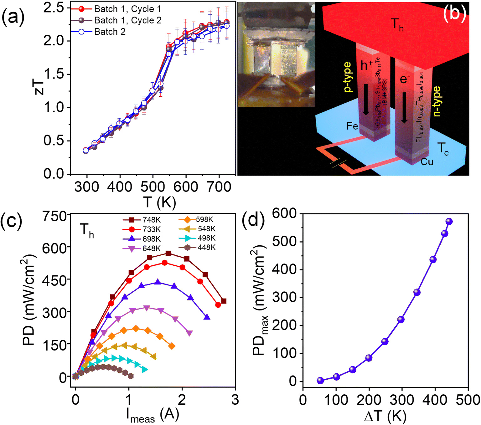 | ||
| Fig. 6 (a) zT of BM + SPS processed Ge0.84Pb0.025Sn0.025Sb0.11Te is reversible over the temperature cycle and batch, (b) schematic representation of the double leg device where the Ge0.84Pb0.025Sn0.025Sb0.11Te (BM + SPS) sample is used as the p-type leg and Pb0.997In0.003Te0.996I0.004 is used as the n-type leg (inset shows the original device photograph), (c) output power density (PD) as a function of measured current at different temperature gradients and (d) maximum output power density (PDmax) as a function of temperature gradient of the double leg TE device. | ||
Motivated by high zT, we have prepared a double leg TE device (Fig. 6b) and measured the power conversion characteristics on a mini-PEM testing system based on the BM + SPS processed Ge0.84Pb0.025Sn0.025Sb0.11Te sample as the p-type leg. For the n-type counterpart, In and I doped PbTe viz. Pb0.997In0.003Te0.996I0.004 is used (fabrication technique discussed in the ESI†).13,44 Fig. S16a ESI† shows the variation of the open circuit voltage (V0) as a function of the temperature difference (ΔT). V0 increases with increase in ΔT due to the increase in the Seebeck coefficient and it reaches a maximum value of 105 mV at ΔT = 448 K. Fig. 6c shows the output power density (PD) of the device as a function of measured current (Imeas) at a particular ΔT. A promising maximum PD (PDmax) ∼590 mW cm−2 at ΔT = 448 K is achieved in the double leg-based TE device (Fig. 6d), which makes our system a potential candidate for efficient mid-temperature power generation application.
Conclusions
In conclusion, we have achieved a remarkably high zT ∼2.3 (with Dulong–Petit Cp, zT is 2.5) at 723 K in an entropy enabled BM + SPS processed Ge0.84Pb0.025Sn0.025Sb0.11Te sample. We have done exclusive cation site alloying of GeTe using Pb and Sn (2.5 mol% each) to increase the configurational entropy of the system. Subsequent doping of aliovalent Sb (11 mol%) optimizes the p-type carrier concentration and leads to further enhancement of the entropy of the system. Finally, high energy ball-milling along with spark plasma sintering (BM + SPS) is performed in a Ge0.84Pb0.025Sn0.025Sb0.11Te sample, which causes drastic enhancement in the Seebeck coefficient ∼210 μV K−1 at room temperature. Such a high value of S is attributed to the extensive valence band convergence effect, where the energy gap between the heavy hole valence band and light hole valence band reduces from 0.23 eV in pristine GeTe to 0.05 eV in the Ge0.84Pb0.025Sn0.025Sb0.11Te (BM + SPS) sample. Lattice thermal conductivity in the BM + SPS processed Ge0.84Pb0.025Sn0.025Sb0.11Te sample reduces to ∼0.63 W m−1 K−1 at room temperature, which is close to the theoretical minimum value (0.3 W m−1 K−1). The ultra-low κL is because of enhanced phonon scattering via extensive cation site disorder, Ge micro/nanoprecipitates along with ripple-like nanostructures and dislocations present in the GeTe matrix. We have fabricated a double-leg device based on the Ge0.84Pb0.025Sn0.025Sb0.11Te (BM + SPS) sample as the p-type leg and In and I doped PbTe as the n-type leg, which shows a promising output power density ∼590 mW cm−2 for ΔT ∼448 K.Author contributions
K. B. proposed the idea and designed the study. A. D. and P. A. carried out the synthesis, characterization, thermoelectric property measurements and other analyses. S. D. helped in double-leg device fabrication. A. D. wrote the first draft; and K. B. contributed to editing the manuscript.Conflicts of interest
The authors declare no competing financial interest.Acknowledgements
K.B. acknowledges support from a Swarnajayanti fellowship, SERB (SB/SJF/2019-20/06) and Sheik Saqr Laboratory. P.A thanks UGC for fellowship. We thank Debattam Sarkar for the fruitful discussion.References
- Q. Yan and M. G. Kanatzidis, Nat. Mater., 2022, 21, 503–513 CrossRef CAS PubMed
.
- T. Ghosh, M. Dutta, D. Sarkar and K. Biswas, J. Am. Chem. Soc., 2022, 144, 10099–10118 CrossRef CAS PubMed
- B. Jiang, Y. Yu, J. Cui, X. Liu, L. Xie, J. Liao, Q. Zhang, Y. Huang, S. Ning, B. Jia, B. Zhu, S. Bai, L. Chen, S. J. Pennycook and J. He, Science, 2021, 371, 830–834 CrossRef CAS PubMed
- X.-L. Shi, J. Zou and Z.-G. Chen, Chem. Rev., 2020, 120, 7399–7515 CrossRef CAS PubMed
- G. Tan, L.-D. Zhao and M. G. Kanatzidis, Chem. Rev., 2016, 116, 12123–12149 CrossRef CAS PubMed
- G. J. Snyder and E. S. Toberer, Nat. Mater., 2008, 7, 105–114 CrossRef CAS PubMed
- Y. Xiao and L.-D. Zhao, Science, 2020, 367, 1196–1197 CrossRef CAS PubMed
- M. Dutta, T. Ghosh and K. Biswas, APL Mater., 2020, 8, 040910 CrossRef CAS
- Y. Pei, X. Shi, A. LaLonde, H. Wang, L. Chen and G. J. Snyder, Nature, 2011, 473, 66–69 CrossRef CAS PubMed
- J. P. Heremans, B. Wiendlocha and A. M. Chamoire, Energy Environ. Sci., 2012, 5, 5510–5530 RSC
- M. Samanta and K. Biswas, J. Am. Chem. Soc., 2017, 139, 9382–9391 CrossRef CAS PubMed
- K. Biswas, J. He, I. D. Blum, C.-I. Wu, T. P. Hogan, D. N. Seidman, V. P. Dravid and M. G. Kanatzidis, Nature, 2012, 489, 414–418 CrossRef CAS PubMed
- D. Sarkar, M. Samanta, T. Ghosh, K. Dolui, S. Das, K. Saurabh, D. Sanyal and K. Biswas, Energy Environ. Sci., 2022, 15, 4625–4635 RSC
- M. Dutta, S. Matteppanavar, M. V. Prasad, J. Pandey, A. Warankar, P. Mandal, A. Soni, U. V. Waghmare and K. Biswas, J. Am. Chem. Soc., 2019, 141, 20293–20299 CrossRef CAS PubMed
- C. Zhou, Y. K. Lee, Y. Yu, S. Byun, Z.-Z. Luo, H. Lee, B. Ge, Y.-L. Lee, X. Chen, J. Y. Lee, O. Cojocaru-Mirédin, H. Chang, J. Im, S.-P. Cho, M. Wuttig, V. P. Dravid, M. G. Kanatzidis and I. Chung, Nat. Mater., 2021, 20, 1378–1384 CrossRef CAS PubMed
- W. He, D. Wang, H. Wu, Y. Xiao, Y. Zhang, D. He, Y. Feng, Y.-J. Hao, J.-F. Dong, R. Chetty, L. Hao, D. Chen, J. Qin, Q. Yang, A. X. Li, J.-M. Song, Y. Zhu, W. Xu, C. Niu, X. Li, G. Wang, C. Liu, M. Ohta, S. J. Pennycock, J. He, J.-F. Li and L.-D. Zhao, Science, 2019, 365, 1418–1424 CrossRef CAS PubMed
- H. Liu, X. Shi, F. Xu, L. Zhang, W. Zhang, L. Chen, Q. Li, C. Uher, T. Day and G. J. Snyder, Nat. Mater., 2012, 11, 422–425 CrossRef CAS PubMed
- A. Banik, T. Ghosh, R. Arora, M. Dutta, J. Pandey, S. Acharya, A. Soni, U. V. Waghmare and K. Biswas, Energy Environ. Sci., 2019, 12, 589–595 RSC
- D. Sarkar, T. Ghosh, S. Roychowdhury, R. Arora, S. Sajan, G. Sheet, U. V. Waghmare and K. Biswas, J. Am. Chem. Soc., 2020, 142, 12237–12244 CrossRef CAS PubMed
- S. Perumal, S. Roychowdhury and K. Biswas, J. Mater. Chem. C, 2016, 4, 7520–7536 RSC
- X. Zhang, Z. Bu, S. Lin, Z. Chen, W. Li and Y. Pei, Joule, 2020, 4, 986–1003 CrossRef CAS
- S. Perumal, S. Roychowdhury, D. S. Negi, R. Datta and K. Biswas, Chem. Mater., 2015, 27, 7171–7178 CrossRef CAS
- Y. Jiang, J. Dong, H.-L. Zhuang, J. Yu, B. Su, H. Li, J. Pei, F.-H. Sun, M. Zhou, H. Hu, J.-W. Li, Z. Han, B.-P. Zhang, T. Mori and J.-F. Li, Nat. Commun., 2022, 13, 1–9 Search PubMed
- J. Li, X. Zhang, Z. Chen, S. Lin, W. Li, J. Shen, I. T. Witting, A. Faghaninia, Y. Chen, A. Jain, L. Chen, G. J. Snyder and Y. Pei, Joule, 2018, 2, 976–987 CrossRef CAS
- W. D. Liu, D. Z. Wang, Q. Liu, W. Zhou, Z. Shao and Z. G. Chen, Adv. Energy Mater., 2020, 10, 2000367 CrossRef CAS
- S. Roychowdhury, M. Samanta, S. Perumal and K. Biswas, Chem. Mater., 2018, 30, 5799–5813 CrossRef CAS
- B. Jiang, W. Wang, S. Liu, Y. Wang, C. Wang, Y. Chen, L. Xie, M. Huang and J. He, Science, 2022, 377, 208–213 CrossRef CAS PubMed
- J. Yang, J. Cai, R. Wang, Z. Guo, X. Tan, G. Liu, Z. Ge and J. Jiang, ACS Appl. Energy Mater., 2021, 4, 12738–12744 CrossRef CAS
- P. Acharyya, S. Roychowdhury, M. Samanta and K. Biswas, J. Am. Chem. Soc., 2020, 142, 20502–20508 CrossRef CAS PubMed
- S. Roychowdhury, R. K. Biswas, M. Dutta, S. K. Pati and K. Biswas, ACS Energy Lett., 2019, 4, 1658–1662 CrossRef CAS
- N. Dragoe and D. Bérardan, Science, 2019, 366, 573–574 CrossRef CAS PubMed
- B. Jiang, Y. Yu, H. Chen, J. Cui, X. Liu, L. Xie and J. He, Nat. Commun., 2021, 12, 1–8 CrossRef PubMed
- Y. Qiu, Y. Jin, D. Wang, M. Guan, W. He, S. Peng, R. Liu, X. Gao and L.-D. Zhao, J. Mater. Chem. A, 2019, 7, 26393–26401 RSC
- S. Zhi, J. Li, L. Hu, J. Li, N. Li, H. Wu, F. Liu, C. Zhang, W. Ao, H. Xie, X. Zhao, S. J. Pennycook and T. Zhu, Adv. Sci., 2021, 8, 2100220 CrossRef CAS PubMed
- R. J. Korkosz, T. C. Chasapis, S.-h. Lo, J. W. Doak, Y. J. Kim, C.-I. Wu, E. Hatzikraniotis, T. P. Hogan, D. N. Seidman, C. Wolverton, V. P. Dravid and M. G. Kanatzidis, J. Am. Chem. Soc., 2014, 136, 3225–3237 CrossRef CAS PubMed
- D. Sarkar, T. Ghosh, A. Banik, S. Roychowdhury, D. Sanyal and K. Biswas, Angew. Chem., Int. Ed., 2020, 59, 11115–11122 CrossRef CAS PubMed
- T. Xing, C. Zhu, Q. Song, H. Huang, J. Xiao, D. Ren, M. Shi, P. Qiu, X. Shi, F. Xu and L. Chen, Adv. Mater., 2021, 33, 2008773 CrossRef CAS PubMed
- Y. Li, T. Zhang, Y. Qin, T. Day, G. J. Snyder, X. Shi and L. Chen, J. Appl. Phys., 2014, 116, 203705 CrossRef
- J. Li, X. Zhang, S. Lin, Z. Chen and Y. Pei, Chem. Mater., 2017, 29, 605–611 CrossRef CAS
- D. G. Cahill, S. K. Watson and R. O. Pohl, Phys. Rev. B: Condens. Matter Mater. Phys., 1992, 46, 6131 CrossRef CAS PubMed
- S. Perumal, M. Samanta, T. Ghosh, U. S. Shenoy, A. K. Bohra, S. Bhattacharya, A. Singh, U. V. Waghmare and K. Biswas, Joule, 2019, 3, 2565–2580 CrossRef CAS
- S. Chandra, U. Bhat, P. Dutta, A. Bhardwaj, R. Datta and K. Biswas, Adv. Mater., 2022, 34, 2203725 CrossRef CAS PubMed
- J. Cui, S. Li, C. Xia, Y. Chen and J. He, J. Materiomics, 2021, 7, 1190–1197 CrossRef
- S. Roychowdhury, T. Ghosh, R. Arora, M. Samanta, L. Xie, N. K. Singh, A. Soni, J. He, U. V. Waghmare and K. Biswas, Science, 2021, 371, 722–727 CrossRef CAS PubMed
Footnote |
| † Electronic supplementary information (ESI) available. See DOI: https://doi.org/10.1039/d2ta09075a |
| This journal is © The Royal Society of Chemistry 2023 |