
Visibly transparent supercapacitors
S.
Kiruthika
 *a,
Namuni
Sneha
a and
Ritu
Gupta
*b
*a,
Namuni
Sneha
a and
Ritu
Gupta
*b
aDepartment of Physics, School of Electrical and Electronics Engineering, SASTRA Deemed to be University, Thanjavur, Tamil Nadu, India. E-mail: kiruthika@ece.sastra.edu
bDepartment of Chemistry, Indian Institute of Technology Jodhpur, India. E-mail: ritu@iitj.ac.in
First published on 25th January 2023
Abstract
Supercapacitors with novel functionalities such as transparency and flexibility are gaining attention to meet the increasing demand for intelligent and smart electronics. Transparent supercapacitors (TSCs) find application in modern appliances such as portable electronics and are especially inevitable for fully integrated transparent devices, thanks to their high-power density, fast charging and discharging ability, and longer life. Transparency is generally achieved by preparing thin films of active electrode material or by adopting lithographic methods for nanostructured electrodes that control the thickness and fill factor without significantly affecting intrinsic conductivity and capacitance. This review discusses all such approaches with a focus on the choice of electrode materials and their design and fabrication for achieving visible transparency in supercapacitors for advanced multifunctional devices. Additionally, it covers the basic concept, device structures, critical parameters, and figure of merit used specifically for transparent supercapacitors. An overview of recent experimental attempts to explore the potential applications of transparent supercapacitors is given, along with the challenges foreseen for the development.
 S. Kiruthika | Dr. S. Kiruthika received her PhD degree (2017) from Jawaharlal Nehru Centre for Advanced Scientific Research, India with DST Inspire Fellowship. After her postdoctoral studies at the Centre for Nano and Soft Matter Sciences, India, she joined as a research scientist (2019) at SASTRA Deemed University, Thanjavur, India. Her research interests include transparent devices, smart energy storage devices, and functional nanomaterials. Currently, she is a visiting scientist at the University of Manchester, UK, supported by SERB-SIRE Grant. |
 Namuni Sneha | Namuni Sneha received her M. S. degree in Chemistry from Osmania University, India, in 2019. Now, she is pursuing her PhD degree under the supervision of Dr S. Kiruthika at SASTRA Deemed University, India. Her research focuses on chemical engineering and fabrication of metal nanonetworks, and their functional applications towards flexible energy devices. |
 Ritu Gupta | Prof. Ritu Gupta obtained her PhD from Jawaharlal Nehru Centre for Advanced Scientific Research (JNCASR), Bangalore, in 2013 and completed postdoctoral research at Purdue University, USA. She is Associate Professor at IIT Jodhpur. Her research group focuses on developing functional nanomaterials for electrochemical energy devices and nanosensors for environmental monitoring and healthcare applications. She has received several prestigious awards, and fellowships as a young researcher. She is a recipient of the INSA Young Scientist Medal 2020, SERB Women Excellence Award-2021, IIT Jodhpur Research Excellence Award Medal 2020, and NASI Young Scientist Platinum Jubilee Award 2021. Presently, she is also a visiting faculty at Technion-Israel Institute of Technology, Israel with prestigious SERB-SIRE fellowship. |
1. Introduction
The emerging demand for transparent optoelectronic devices urges technological innovations that lead to high optical transmittance without sacrificing performance.1,2 Transparent technology provides more visual information about electronic gadgets than conventional non-transparent ones.3,4 An enormous effort has been made to transform non-transparent circuits, transistors, and displays to be almost visibly clear.5–8 Technologically advanced electronic devices can be realized by integrating with transparent energy storage devices.9 Supercapacitors are new generation energy storage devices for portable electronics due to their compact, low cost, easy processability, higher power densities than batteries, and long cycle life.10–12 Supercapacitors are an ideal alternative to batteries for low power/energy requirements when there is a need for high power delivery.13 Energy is stored in electrochemical capacitors either by electrochemical double-layer formation on absorbing ions at the electrode–electrolyte interface or rapid redox reactions (pseudo-capacitive).14 The device performance has been improved by developing novel nanostructured materials with sub-nanometer pores for future systems such as hybrid electric vehicles and industrial equipment.8 Since the specific capacitance of a conventional supercapacitor depends on the electrode material's mass, area, or volume, a transparent supercapacitor is still a counterintuitive concept and is nascent. Unlike conventional energy storage devices, transparent supercapacitors are highly adaptable to next-generation flexible transparent electronics, especially in wearable devices, sensors, and health monitors.15–20 Developing transparent electrodes with excellent optoelectronic properties and electrochemical and mechanical stability is significant for constructing flexible transparent supercapacitors. Besides several evaluation metrics for transparent electrodes, various transparent conducting electrodes used in supercapacitors are summarized. The different strategies for fabricating transparent supercapacitors and their applications are discussed in detail. This investigation of the transparent supercapacitor is a branch of transparent electronics that bridges materials and chemical sciences with information technology.4 Hence a detailed discussion of the transparent supercapacitor is necessary.1.1. Device architecture of transparent supercapacitors
A transparent supercapacitor comprises a substrate, current collector, active material, and electrolyte, where all components must be essentially transparent.4 The term electrode in a supercapacitor generally refers to a combination of the active material, current collector, and substrate. Supercapacitors are classified as film supercapacitors and micro-supercapacitors based on electrode alignment.21 Unlike typical supercapacitors, transparent devices demand visible transparency from every component involved in fabrication, from active materials, electrolytes, and separators to current collectors, including packaging.1 This unique requirement poses a significant challenge in developing transparent energy storage devices as, in general, none are usually transparent except for the electrolyte.9,22,23 On the other hand, one may have to choose wisely the transparent conducting materials considering various parameters like the figure of merit (FoM), specular and diffusive transmittance, haze, and bandgap other than electrical conductivity.24–26In film supercapacitors, two transparent electrodes have a sandwich configuration with a separator or solid-state gel electrolyte. Based on the operating mechanism, the supercapacitor is symmetric if the active material coated on both electrodes is identical; otherwise, it is denoted as an asymmetric supercapacitor.27–29 Asymmetric configurations basically have an electric double-layer capacitance (EDLC) electrode and a pseudocapacitance electrode sandwiched with a separator or gel electrolyte. EDLC stores energy via the fast and highly reversible electrostatic adsorption/desorption of electrolyte ions onto the electrochemically active and stable electrode as a double layer under applied voltage bias. The more commonly used carbon-based electrode materials like CNTs, graphene, and carbon black are a few EDLC electrodes.30 Pseudocapacitance stores charges via a reversible faradaic charge transfer. The typical examples of pseudocapacitance materials are transition metal oxides (MnO2 and Co3O4), hydroxides (Ni(OH)2), carbides (Ti3C2), and sulfides (CuS and MoS2); conducting polymers like polyaniline (PANI) and polypyrrole (PPy).21,31 Furthermore, the electrode should possess a high specific surface area for fast ion/electron transfer for superior performance of storage devices.4
On the other hand, planar 2D printed micro-supercapacitors (MSCs) have recently received much interest because of their excellent stability towards deformations, high electrochemical performance, and ease of on-chip integration with various flexible and functional electronic devices. MSCs have a substantially longer working lifetime, around 100![[thin space (1/6-em)]](https://www.rsc.org/images/entities/char_2009.gif) 000 cycles, a faster charging/discharging rate, and a higher power density than flexible batteries. Micro-supercapacitors have attracted attention for applications such as implanted biochips and sensors as they satisfy the demands like long cycle life, quick charge–discharge capability, and high-power density.32
000 cycles, a faster charging/discharging rate, and a higher power density than flexible batteries. Micro-supercapacitors have attracted attention for applications such as implanted biochips and sensors as they satisfy the demands like long cycle life, quick charge–discharge capability, and high-power density.32
1.2. Evaluation metrics
An ideal transparent electrode for an energy storage device should possess low sheet resistance (RS ∼ 10 Ω sq−1), high transmittance (T ∼ 90%), and high capacitance. For a material to be transparent in the visible region of the electromagnetic spectrum (400–700 nm), it must have a bandgap > 3.1 eV (400 nm).33 Typically, insulators have a bandgap of 3–5 eV, whereas oxide-based conductors usually show a high bandgap (>3 eV).34 In a semiconductor with a filled valence band and an empty conduction band, band gaps are around 2 eV.35 The electrode transmittance is calculated at 550 nm in the UV-visible spectrum, and sheet resistance can be obtained using two or four-probe geometry.4 More commonly, electrodes with high transmittance are realized by reducing the thickness of active materials, which, in turn, significantly affects the sheet resistance, which reduces the capacitance. Therefore, there is always a trade-off between these two parameters.36 To avoid difficulty in direct comparison, a few performance metrics are derived for easy evaluation of TCE performance. When it comes to the commercial aspects of the device, the chemical and mechanical stabilities of electrodes, their associated cost, and stability towards deformation should also be deeply considered.37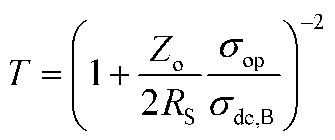 | (1) |
Assuming sheet resistance to be inverse of dc conductivity with respect to thickness, the ratio terms in the equation can be simplified in terms of σop as below:
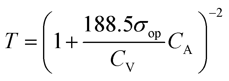
| T = (1 + 188.5σopt)−2 | (2) |
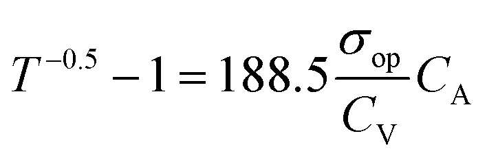
However, in the case of transparent supercapacitors, the transmittance of the electrodes needs to be specified with respect to the charge storage capacity. A new capacitive figure of merit (FoMc) value is calculated from the areal-specific capacitance (CA) and optical conductivity (σop) ratio.39 FoMc is obtained by plotting a series of T versus CA. The higher the FoMc values, the better the storage capacity of the electrodes at a given transmittance. It is worth noting that an electrode with ultra-high transmittance with an ultrathin material thickness will eventually result in high RS with compromised areal capacitance (CA). The trade-off between %T and CA can be quantified as per eqn (3), and % T can also be obtained using eqn (2).39,40
 | (3) |
Furthermore, CV/σop and CV values can be calculated from eqn (4) and (5) below.39,40
 | (4) |
| CV = FoMc × σop | (5) |
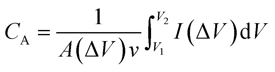
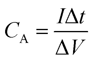
C A values (F cm−2) are obtained using eqn (6).41
 | (6) |
 | (7) |
 | (8) |
 | (9) |
Specific capacitance realized with aqueous acids is usually greater than with organic electrolytes. However, organic electrolytes are often preferred as they can offer higher operation voltage (∼2.7 V) in symmetric configuration, while aqueous electrolytes provide only 1.2 V.
2. Electrode materials for transparent supercapacitors
The device with high transmittance is achieved either by reducing the active material thickness or decreasing the material loading, thus compromising the energy storage performance. Consequently, there is always a trade-off between transmittance and capacitance. There is an urge to find a cost-effective alternative to tin-doped indium oxide (ITO) as it suffers from price elevation due to increasing demand and scarcity of indium. Due to its oxide nature, the brittleness makes it implausible for adoption in futuristic large-area flexible electronics. The alternative new-generation transparent conducting materials that emerged in the last decade can be broadly classified into ultra-thin conducting materials, conducting networks, and hybrid structures, as shown in Fig. 1.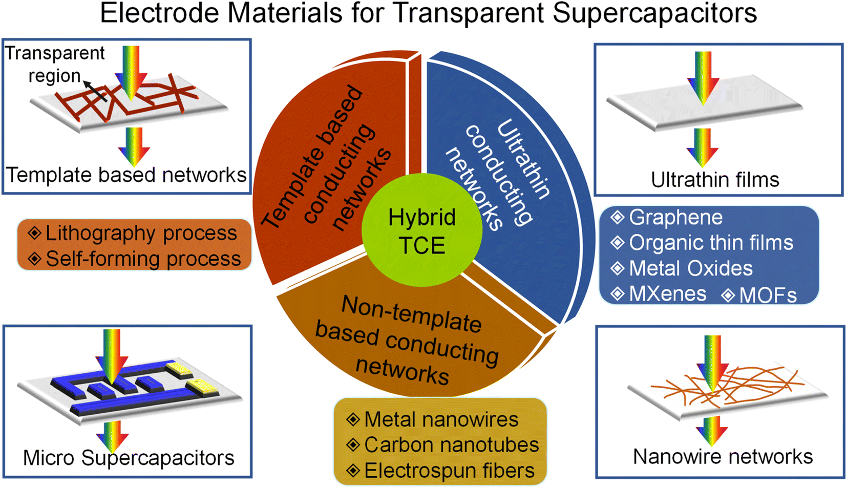 | ||
| Fig. 1 Typical transparent conducting electrodes used for fabricating transparent supercapacitors. | ||
The simplest way to make transparent electrodes is by coating ultra-thin films of conducting material on a transparent substrate such as glass, polyethylene terephthalate (PET), polyethylene (PE), polydimethylsiloxane (PDMS), and polyurethane acrylate. The deciding factor for the film to be visibly transparent in the electromagnetic spectrum is maintaining the film thickness below the light absorption thickness. There are techniques developed for fabricating films that are sufficiently thin to achieve high optical transparency. However, this also increases the sheet resistance and thus deteriorates the current collection from the electrodes. This points out the trade-off between transparency, sheet resistance, and charge storage capacity. In template-based and non-template-based conducting networks, the electrodes were realized from interconnected networks prepared via various lithography, self-forming processes, and 1D nanomaterials. Hybrid TCEs combining two or more different electrode materials provide a promising pathway for overcoming the shortcomings of individual ones.
2.1. Ultra-thin conducting electrodes
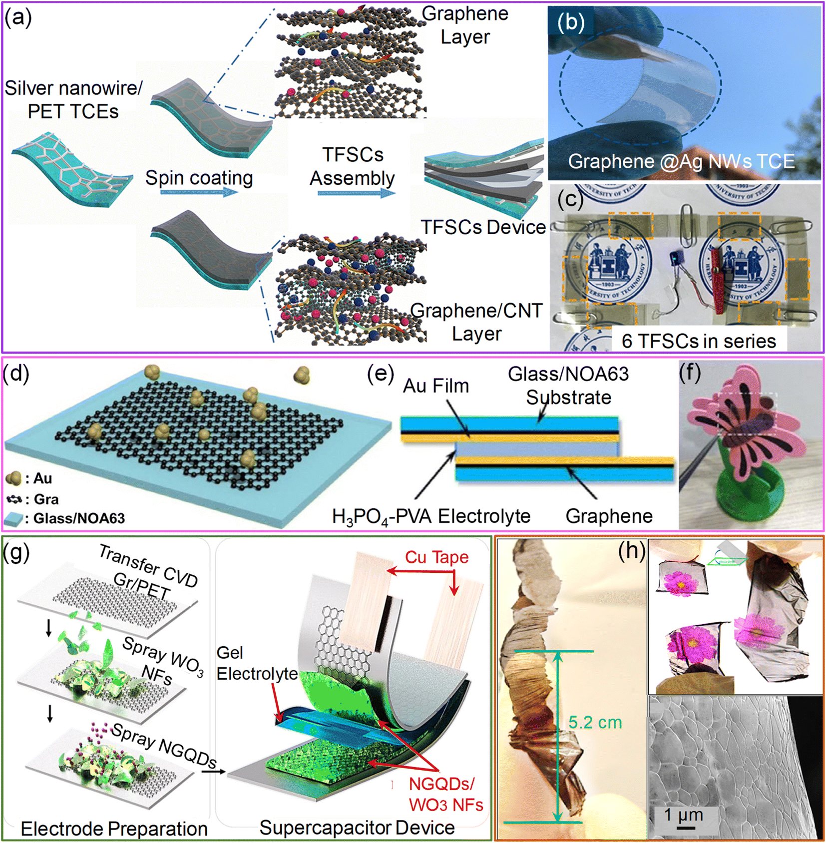 | ||
| Fig. 2 Graphene: (a) schematic illustration of the fabrication of a transparent and flexible supercapacitor (TFSC) device using hybrid graphene/CNTs/Ag NWs. (b) Photographs of the prepared graphene@AgNW TCE and glowing LED by connecting six TFSCs in series (c). Reproduced with permission from ref. 56. Copyright 2018 American Chemical Society. Schematic representations of Au thin film fabrication over a graphene layer (d) and (e) supercapacitor device using a gel electrolyte. (f) Photograph of the supercapacitor device fabricated with composite materials. Reprinted with permission from ref. 61. Copyright 2019 by Elsevier. (g) Flexible and transparent supercapacitor fabricated using tungsten oxide nanoflakes, and nitrogen-doped graphene quantum dot (WO3 NFs/NGQD) based electrodes. Reproduced with permission from ref. 62. Copyright 2020 by Elsevier. (h) Photograph of a sheet of large-area, flexible, freestanding, and transparent graphene paper (FFTGP) (left). Photographs in the upper right show FFT-GP sheets in various angles, and the lower right SEM image shows prism-like graphene microstructures of FFT-GP sheets. Reproduced with permission from ref. 42. Copyright 2015 American Chemical Society. | ||
On the other hand, CVD-grown graphene films possess high optical transmittance and low sheet resistance with desirable robustness towards mechanical deformations. The transparent supercapacitors fabricated by sandwiching CVD-grown graphene layers (transferred to desired substrates) between electrolytes yielded a capacitance of several μF cm−2 with high transparency.57–60 However, the sheet resistance of monolayer graphene is several hundred Ω sq−1. The deposition of an ultrathin Au film (7 nm) over monolayer graphene brought sheet resistance down to 24.6 Ω sq−1 with a transmittance of ∼75% at 520 nm (Fig. 2d). An Au–graphene-based supercapacitor fabricated by sandwiching a H3PO4–PVA gel electrolyte yields an areal capacitance of ∼82 μF cm−2, nearly 17 times higher than that of bare graphene devices (see Fig. 2e and f). A flexible supercapacitor fabricated with Au–graphene composite electrodes exhibits only 12.5% degradation even after 1800 bending cycles (bending radius, 5 mm).61 In another example, upon CVD-grown graphene which was transferred to a PET substrate, 2D tungsten-oxide nanoflakes and 0D nitrogen-doped graphene quantum dots were deposited to develop a high-performance flexible, transparent supercapacitor (Fig. 2g). This technique is highly plausible for large-scale fabrication and patterning due to the simple synthesis methods and deposition through the spray-coating process. The fabricated symmetric supercapacitor exhibited a specific capacitance of ∼180 F g−1 with 70% transmittance with energy and power densities of 15.8 W h kg−1 and 360.1 W kg−1, respectively.62
Besides the CVD technique, graphene layers were directly grown on a SiO2/Si substrate via a rapid thermal annealing (RTA) process. The advantages of the RTA process include minimal time consumption for fabrication (1–2 min) due to the rapid cooling to room temperature. They require no gas precursors, thus making them suitable for large-area fabrication. The supercapacitors fabricated by sandwiching two such graphene/PET electrodes with a PVA/H3PO4 gel electrolyte have shown ∼65% transmittance with energy and power densities of 3 W h kg−1 and ∼500 kW kg−1.63
Making a vertically oriented 3D graphene network could be a crucial step for exploring graphene to its full potential for supercapacitor applications. Generally, efforts have focused on controlling the morphology and properties of 3D microscopic structures to obtain networks with good conductivity and large surface areas. However, for optoelectronic systems, transmittance is a crucial property to be addressed. In an example, NaCl powder was used as a template for the growth of transparent freestanding graphene paper using a microwave plasma-enhanced chemical vapor deposition (MPECVD) system (see Fig. 2h).42 In a typical fabrication process, the carbon source was produced by decomposing CH4 under high-temperature annealing (560 °C). At a microwave power of 750 W, a graphene base layer was formed on the Si substrate. NaCl powder melted entirely under a high-energy electric field and formed a thin layer over the base graphene layer. After completing the growth process, the NaCl template was etched by a physical sputtering etching process to achieve freestanding flexible and transparent graphene sheets (Fig. 2h). When employed in supercapacitor fabrication, these sheets enhanced the capacitance ∼1000 times compared to CVD-grown graphene supercapacitors.42 Overall, graphene with ultrahigh transparency (>90%) and low resistance (∼50 Ω sq−1), and the high specific surface area for charge storage hold immense potential for transparent supercapacitor applications.
2.1.2.1. PEDOT:PSS. The usage of PEDOT as an electrode material in electrochemical capacitors dates back to 1997. The addition of PSS enhances the conductivity of PEDOT and thus helps in improving capacitance.66,67 For instance, PEDOT:PSS electrodes sandwiched with H3PO4/PVA gel electrolytes result in high-performance transparent all-solid-state supercapacitors with an areal (gravimetric) capacitance of ∼4.72 mF cm−2 (27.76 F g−1). With increasing PEDOT:PSS layer thickness, the specific capacitance increased drastically with an increase in the mass of the active materials (PEDOT), whereas the transmittance of the device decreased to ∼55% at 550 nm. The maximum power and energy densities of 0.036 W cm−2 and 0.38 mW h cm−2 were achieved.68 Besides PSS, secondary dopants like sorbitol, H2SO4, dimethyl sulfoxide, methanol, and ethylene glycol dramatically increase the electrical conductivity.25 In another report, the conductivity of the PEDOT:PSS layer was enhanced by dipping the films in formic acid (FA) for just a few seconds at room temperature.25 There was an exponential decrease in sheet resistance by three orders of magnitude from 1.5 × 10⁵ Ω sq−1 to 102 Ω sq−1. The FoM value (σdc/σop) of the PEDOT:PSS films dipped in FA is 39, much higher than that of SWCNT-based electrodes. PEDOT: PSS films doped with FA have shown excellent electrochemical performance with an areal capacitance (CA) of 1.9 mF cm−2 and 0.18 mF cm−2 for 70% and 99% transparent films, respectively.25 Further enhancement in the capacitance of PEDOT:PSS electrodes was forbidden by their intrinsic optoelectronic properties (RS > 100 Ω sq−1).
In this respect, hybrid electrodes are ideal for reducing the RS to below 10 Ω sq−1. The hybrid electrodes composed of metal nanowires, grids, fibers, and nano- and micro-meshes with PEDOT:PSS improve the electrochemical performance due to the highly conducting metal backbone structures. For instance, embedded AgNWs/PEDOT:PSS electrodes with a novel interlayer composed of Ni(OH)2 and polyethyleneimine ethoxylated (PEIE) yield a remarkable volumetric capacitance of 443 F cm−3 with 86% transparency. In addition, the bifunctional electrochromic supercapacitor device fabricated using this hybrid electrode shows a fast-switching speed with cycle stability of 10000 charge–discharge cycles. The main reason for such enhancement in capacitance is the improved pore density of PEDOT:PSS with the Ni(OH)2–PEIE interlayer.69 Later, an ultra-smooth embedded PEDOT:PSS/AgNFs/NOA-63 hybrid electrode was fabricated by sandwiching free-standing Ag nanofibers with a PEDOT:PSS film and photopolymer Norland Optical Adhesive, NOA 63. The resulting electrode exhibited high transmittance (85%), low sheet resistance (∼2.1 Ω sq−1), and excellent mechanical stability. The transparent supercapacitor device fabricated with a hybrid electrode possesses excellent electrochemical performance (3.64 mF cm−2) and mechanical flexibility (Fig. 3a–c).70
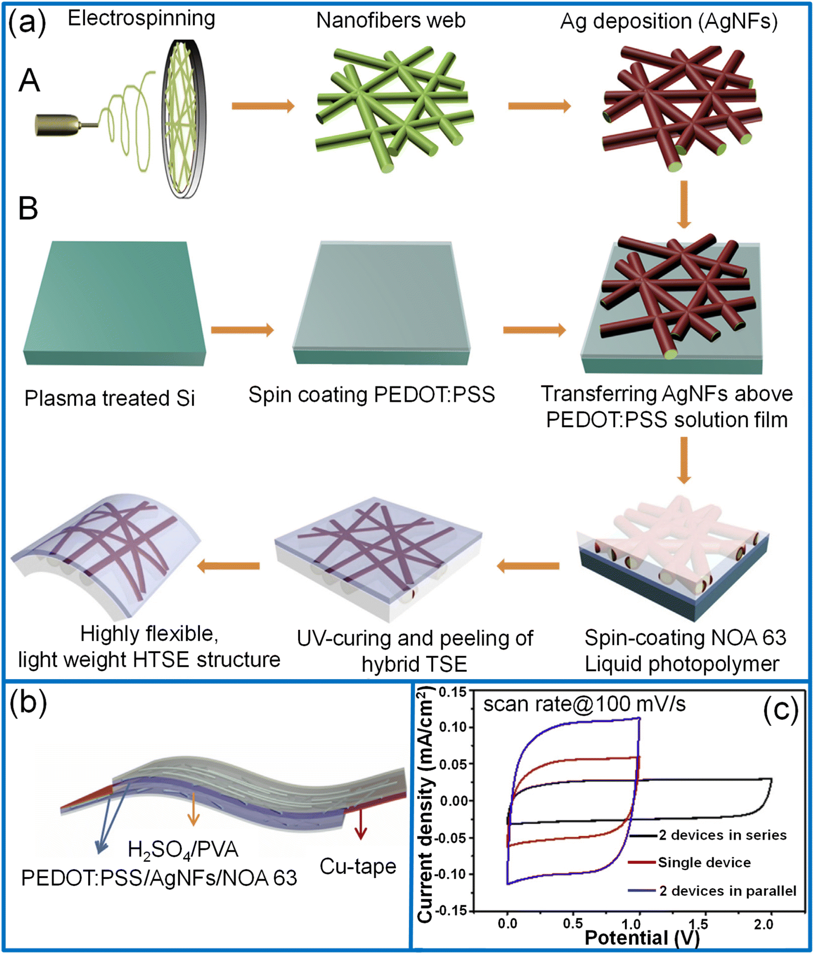 | ||
| Fig. 3 PEDOT:PSS: (a) schematic illustration of the fabrication of the PEDOT:PSS/Ag nanofibers/NOA 63 hybrid transparent supercapacitor electrode (HTSE) structure. (b) Schematic diagram of the transparent solid-state supercapacitor device fabricated by assembling two HTSEs with a gel electrolyte in between. (c) Cyclic voltammogram curves of a single solid-state supercapacitor device compared with two devices connected in series and parallel configurations at a scan rate of 100 mV s−1. Reprinted with permission from ref. 70. Copyright 2019 by Elsevier. | ||
2.1.2.2. Polypyrrole. Due to its high storage capacity, environmental stability, and cost-effective fabrication, polypyrrole (PPy) has been used as an active material for supercapacitors since 1960.71–73 A simple, cost-effective solution-processing interfacial chemical oxidative polymerization method is highly considered for large-area fabrication.74,75 In this process, the polymerization time controls the prepared film's thickness, haze, and conductivity. For example, Jiao et al. synthesized a PPy/PET film with the dimensions of 25 × 15 cm2 with good transparency (71%), low haze (1.4%) and sheet resistance (0.78 kΩ sq−1) (see Fig. 4a).40 In the preparation process, a PET film was floated on the surface of a solution containing iron chloride and 2,6-naphthalene disulfonic acid disodium dissolved in an organic solvent and water mixture which was maintained at ∼4 °C. The pyrrole monomer dissolved in a similar organic solvent/water mixture was slowly added to the above mixture solution to initiate the polymerization in the interfacial region between PET and the liquid. During the polymerization process, a thin layer of PPy was deposited on the lower surface of the PET film. After the desired deposition time, the PPy/PET film was taken out, rinsed, and dried to obtain the TCE. During the synthesis, the organic solvent added in a small volume enhances the solubility of the pyrrole monomer and induces homogeneous polymerization on the surface of the PET. In order to make PET float on the liquid surface, the optimum ratio of methanol and water (1
:9) was taken as the PET surface is hydrophobic and organic solvents wet the PET surface more easily and help in easier absorption of PPy monomers on the PET surface. It is also noticed that the mole ratio of pyrrole and iron chloride (FeCl3) must be maintained above one for the uniform and continuous formation of the PPy film. Compared to electrochemical oxidation, this method is highly facile, less time-consuming, and cost-effective. The electrochemical performance of the symmetric sandwich-structured supercapacitor was demonstrated by assembling two PPy electrodes with a H3PO4/PVA gel electrolyte. The fabricated large-area supercapacitor (20 × 15 cm2) exhibited low haze (1.54%) with nearly 47% transmittance at 550 nm with a specific areal capacitance of 1.45 mF cm−2 (Fig. 4b and c).40 Using a strategy of DMF etchant-writing, the desired interdigital channel pattern for the micro-supercapacitors was obtained on the PET substrate. The fabricated micro-supercapacitor showed ∼70% transmittance and yielded areal capacitance, energy, and power densities of 1.64 mF cm−2, 5 mW h cm−3, and 67.3 mW cm−3, respectively.40 Direct electro-polymerization onto the transparent current collector is another more promising way of fabrication. Moon et al. first reported an Ag/Au/PPy flexible transparent electrode by direct electro-polymerization of PPy over a conducting network (Fig. 4d).76 The thickness of the PPy coating over the nanowire network was determined by sweep cycles at 0.2 V s−1 in the voltage range from 0 to 1.0 V. With an increasing number of deposition cycles (20), the diameter of Ag/Au/PPy nanowires increased to 136 nm with 62% transmittance. The nanowires with three sweep cycles exhibited high optoelectronic performance (∼85% transmittance) and capacitance (Fig. 4e). In addition, the fabricated flexible symmetric supercapacitor had a negligible capacitance loss while bending (bending radius, 5–30 mm).76
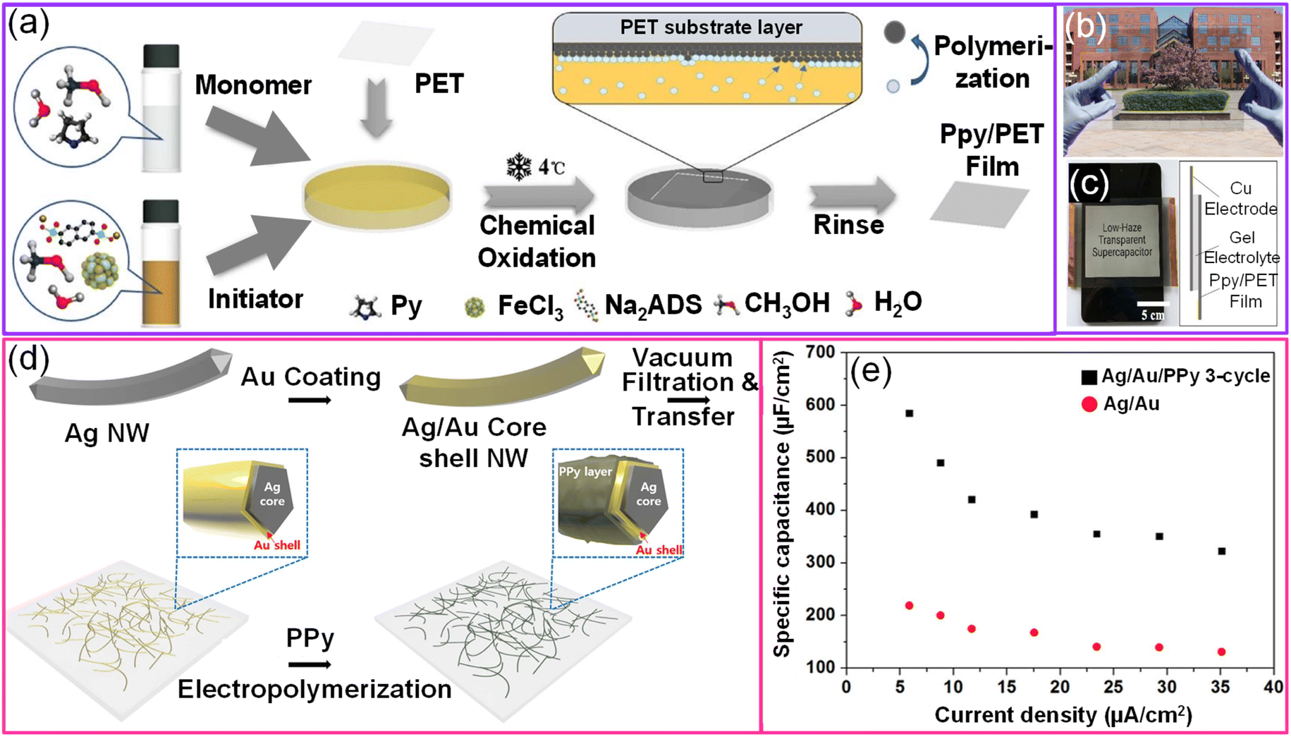 | ||
| Fig. 4 Polypyrrole: (a) schematic representation of fabrication of PPy/PET-based transparent conducting low-haze electrodes through an interfacial polymerization technique. (b) Photograph of a large-area TCE (17 × 22 cm2) and a fabricated large-area supercapacitor (c). Reprinted with permission from ref. 40. Copyright 2018 American Chemical Society. (d) Schematic representation of fabrication steps for Ag/Au/PPy electrodes. (e) The dependence of the specific areal capacitance of bare Ag/Au NWs and Ag/Au/PPy NWs on the discharging current densities. Adapted with permission from ref. 76. Copyright 2017 by Springer Nature. | ||
2.1.3.1. Tin-doped indium oxide (ITO). Transparent conducting metal oxide coatings are commonly used as a current collector for transparent supercapacitors. For instance, transparent, flexible, and solid-state supercapacitors have been fabricated on ITO using room-temperature ionic liquid (RTIL) gel. The RTIL gel composed of 1-butyl-3-methylimidazolium chloride ([BMIM][Cl]) and 6 wt% cellulose nanoparticles forms a transparent electrolyte after drying. ITO is deposited on a polyethylene naphthalate (PEN) substrate through high target utilization sputtering (HiTUS) technology that yields a smooth surface. The average ITO thickness on the PEN substrate is ∼470 nm with 92% transmittance (between 450 nm and 800 nm) and 7.7 Ω sq−1 sheet resistance. The specific capacitance calculated from galvanostatic charge–discharge measurements of ITO/[BMIM][Cl]/ITO is ∼18 F g−1. This is the first EDLC-type supercapacitor based on an ionic liquid gel.77 The deposition of transition metal oxides like Co3O4, MnO2, and RuO2 enhances the capacitance and cycling life compared to bare ITO electrodes due to high electrochemical performance. Liu et al. have coated Co3O4 nanocrystals synthesized via a laser ablation in liquid (LAL) technique on an ITO/PET (15 Ω sq−1) substrate and fabricated a solid-state supercapacitor by assembling two such electrodes with a PVA/H3PO4 gel electrolyte. The cyclic voltammogram curves with two strong redox peaks indicate the pseudocapacitive nature of the supercapacitor. The supercapacitor delivers a specific capacitance of 172 F g−1 and an areal capacitance of 6.03 mF cm−2 with maximum energy and power densities of 3.01 W h kg−1 and 1.152 kW kg−1. The fabricated supercapacitor is 51% transparent at a wavelength of 550 nm. It is worth noting that even after 20
000 cycles, the capacitance retention is 100% which decreased to 93% after 30000 cycles. The main factors contributing to excellent cycling stability are the high surface-to-volume ratio and the clean surface (devoid of contaminants) of Co3O4 nanocrystals.78 Similarly, MnO2 thin films were electrochemically deposited onto an ITO/PET substrate due to their high theoretical specific capacitance, low cost, and eco-friendly properties. The transparent symmetrical supercapacitor device with two ITO/MnO2 electrodes sandwiched with a K2SO4/SiO2 composite gel electrolyte exhibit a capacitance of 15 mF cm−2.79 The MnO2 thin-film electrodes have also been directly grown on ITO/PET using a facile and inexpensive chemical bath deposition technique. The MnO2 thin film offers a specular transmittance of 77.4% at 550 nm. The ITO/MnO2 thin-film electrodes exhibited a specific capacitance and areal capacitance of ∼230 F g−1 and 9.2 mF cm−2 in a 1 M Na2SO4 electrolyte.80 As an alternative, ligand-mediated layer-by-layer (LbL) assembly is another simple process that utilizes complementary interactions between the molecules to prepare ultrathin composite films with the desired thickness, compositions, and functionalities. High-energy pseudocapacitive (OA–MnO) nanoparticles and conducting oxide (OAm–ITO) nanoparticles were LbL-assembled using a ligand exchange between native ligands (oleic acid (OA)/oleylamine (OAm)) and tricarballylic acid (TC), a small multidentate linker (Fig. 5a).81 The introduced TC linker substantially reduced the inter-distance between the adjacent NPs, thereby reducing the resistance of the electrodes. Additionally, the periodic deposition of ITO NPs and MnO NPs significantly enhances the areal capacitance by reducing the charge transfer resistance without substantial transmittance loss. The electrochemical storage capability of (MnO NP/TC/ITO NP/TC)50 electrodes was investigated in a 0.5 M Na2SO4 electrolyte. After the deposition of ITO NPs, the areal capacitance of the device increased to 40.5 mF cm−2 (T%, 60.8%) from the initial value of 24.6 mF cm−2 (T%, 61.6) with no ITO NPs.81 In another example, standing ITO nanopillars (T ∼ 64%) fabricated using a radiofrequency (RF) sputtering technique have been used as a current collector instead of ITO films (Fig. 5b). The electrochemical deposition of pseudocapacitive materials like RuO2 on ITO nanopillars enhances the specific capacitance (1235 F g−1) due to facilitated charge transfer and ion diffusion across standing coaxial nanostructures (Fig. 5c and d).82
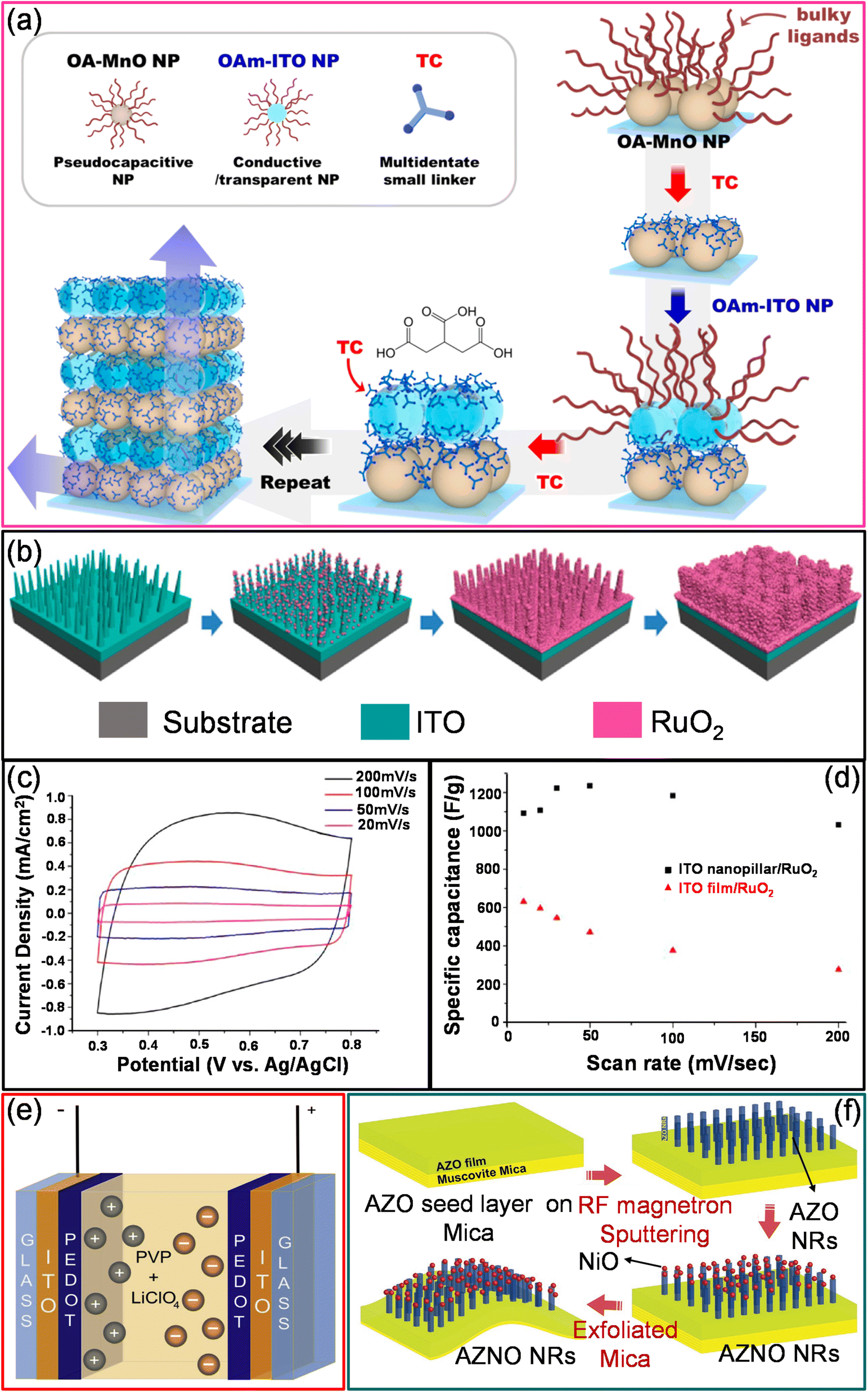 | ||
| Fig. 5 Metal oxides: (a) schematic diagram of the formation of a MnO NP-based flexible solid-state transparent supercapacitor (TSC) with ITO NPs. Reproduced with permission from ref. 81. Copyright 2020 American Chemical Society. (b) Schematic representation of fabrication of the coaxial ITO and RuO2-based core–shell electrode. (c) CV curves of ITO nanopillars coated with RuO2 (30 cycles) at various scan rates. (d) Comparison of the specific capacitance of bare ITO nanopillars and RuO2-coated ITO nanopillars at various scan rates. Reproduced with permission from ref. 82. Copyright 2014 American Chemical Society. (e) Schematic diagram illustrating the electrode configuration of a transparent supercapacitor with ITO/PEDOT-based electrodes. Reprinted with permission from ref. 83. Copyright 2013 by Elsevier. (f) Schematic illustrations of the AZO nanorod and AZO/NiO nanorod heterostructure fabrication process using RF magnetron sputtering on a muscovite substrate. Reproduced with permission from ref. 85. Copyright 2020 by John Wiley and Sons. | ||
On the other hand, ITO-based heterogeneous film supercapacitors fabricated with CNTs and PEDOT exhibit high specific capacitance. Instead of bare ITO, ITO/PEDOT electrodes have also been utilized. By sandwiching two ITO/PEDOT electrodes with PVP/LiClO4 solid polymer electrolyte films, a supercapacitor with a maximum transmittance of ∼50% between 370 and 770 nm with a maximum specific capacitance of 15 F g−1 is obtained (Fig. 5e).83 Chen et al. realized transparent supercapacitors with 30 wt% In2O3 nanowires and CNT composites. The device offers ∼50% transmittance with energy and power densities of 1.29 W h kg−1 and 7.48 kW kg−1, respectively.84
2.1.3.2. Aluminum-doped zinc oxide (AZO). AZO is another commonly used transparent conducting material for commercial applications mainly due to its excellent electrical and optical properties, low cost, and non-toxicity. Furthermore, oxides with 1D nanostructures like nanowires, nanorods, nanofibers, etc., are of great interest due to their high surface area with short carrier diffusion lengths. Le et al. have prepared flexible and transparent AZO nanorods and AZO/NiO nanorods on mica through radio-frequency (RF) sputtering.85 Its potential for energy storage applications was explored by sandwiching two AZO/NiO nanorod electrodes with a PVA/KOH gel electrolyte, as shown in Fig. 5f. The specific capacitance calculated from the galvanostatic charge–discharge curve is 3.4 mF cm−2 with 80% transmittance. The energy and power densities of the device are 45.38 nW h cm−2 and 4.97 μW h cm−2, respectively.85
2.1.3.3. Molybdenum trioxide (MoO3). An ultralong molybdenum trioxide nanobelts with an average length of 200 μm with a length-to-width ratio of almost 1000 were synthesized using the hydrothermal technique. The reaction completion was evident from the change in the color of orange peroxomolybdic acid into a white suspension of MoO3 nanobelts. The prepared nanobelts remained well dispersed in ethanol without aggregation, even for a year. The formed nanobelts are shown to be thermochemically stable up to 788 °C. Freestanding transparent and mechanically flexible yet robust MoO3 nanopaper with a thickness of several hundred nanometers was prepared by simple vacuum filtration of MoO3 nanobelt suspension and the subsequent peeling-off process. The transparent nanopaper is a 3D network of MoO3 nanobelts with large pores in-between nanobelts. These pores highly facilitate ion diffusion in freestanding 3D networks. The nanopaper with 0.076 mg cm−2 offers ∼90% transmittance. The symmetric supercapacitor device with two MoO3 nanopaper assembled with a 5 M LiCl or PVA/LiCl gel electrolyte exhibits a specific capacitance of ∼258 F g−1, which slowly decreased to ∼95 F g−1 for a scan rate of 200 mV s−1. The device exhibits 96.5% capacitance retention even after 20
000 cycles of charge–discharge. The device's maximum energy and power densities were 22.89 W h kg−1 and 10.1 kW kg−1, respectively.86
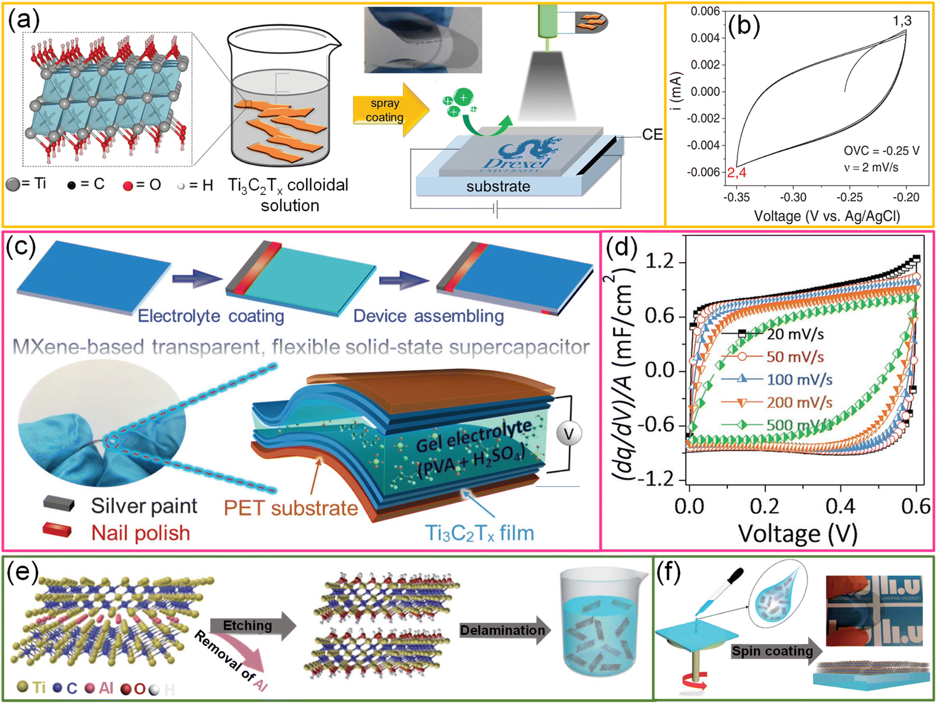 | ||
| Fig. 6 MXenes: (a) schematic representation of fabrication of a Ti3C2Tx thin film through the spray coating process. The structure of Ti3C2Tx is given in the box where Ti, O, H and C represent gray, red, white, and black, respectively. Inset shows the high degree of flexibility of the Ti3C2Tx thin film. (b) CV curve of the Ti3C2Tx MXene thin film in a 3-electrode configuration. Reproduced with permission from ref. 91. Copyright 2016 by John Wiley and Sons. (c) Schematic representing the fabrication of a Ti3C2Tx MXene-based flexible solid-state transparent supercapacitor device and its corresponding cyclic voltammogram curves are given in (d). Reproduced with permission from ref. 39. Copyright 2017 by John Wiley and Sons. (e) Schematic depiction of preparation of the Ti3AlC2 precursor using a minimally intensive layer delamination (MILD) process. (f) Schematic illustration of the preparation of a MXene-based transparent electrode via a spin coating approach. Reproduced from ref. 92 with permission from the Royal Society of Chemistry. | ||
To explore the performance of all MXene-based supercapacitor devices, two Ti3C2Tx TCEs (91%, T) are sandwiched with a gel electrolyte, and the fabricated symmetric supercapacitor devices have shown ∼80% transmittance (Fig. 6c).39 The capacitive nature of the device is evidenced by its linear galvanostatic charge–discharge curves, rectangular shapes of cyclic voltammograms, and quick current response upon voltage reversal (Fig. 6d). The areal capacitance of the symmetric device is 0.86 mF cm−2. The asymmetric device was fabricated by sandwiching SWCNTs and Ti3C2Tx TCEs in sequence. Due to the broader voltage window offered in an asymmetric configuration, the energy and power densities of the device were enhanced to 0.05 μW h cm−2 and 2.4 μW cm−2, respectively.39 In another example, Qin et al. fabricated Ti3C2Tx MXene-based flexible, semitransparent solid-state photovoltaic supercapacitors (PSCs) through the vertical stacking method.92 The Ti3C2Tx film aligned parallel to the substrate while spin coating, demonstrating outstanding conductivity, flexibility, and transmittance (Fig. 6e and f). These properties make the MXene film an efficient TCE for OPVs with a high photoconversion efficiency of 13.6% and an active material for supercapacitors resulting in a high volumetric capacitance of 502 F cm−3 with a high average transmittance of 33.5%. In addition, the usage of organic solid ion gel electrolytes compared to water-based electrolytes increases the cycling stability of the device.92 Although MXene-based devices exhibit excellent charge-storage capability and optoelectronic properties, the instability of MXene dispersions and devices in the ambient environment is the bottleneck. However, the shelf-life of MXene-based dispersions is extended by proper storage. Besides the stability, the high cost of Ti3AlC2 MAX (∼$550/150 g) is the other biggest challenge hindering MXene-based products from entering the market.37
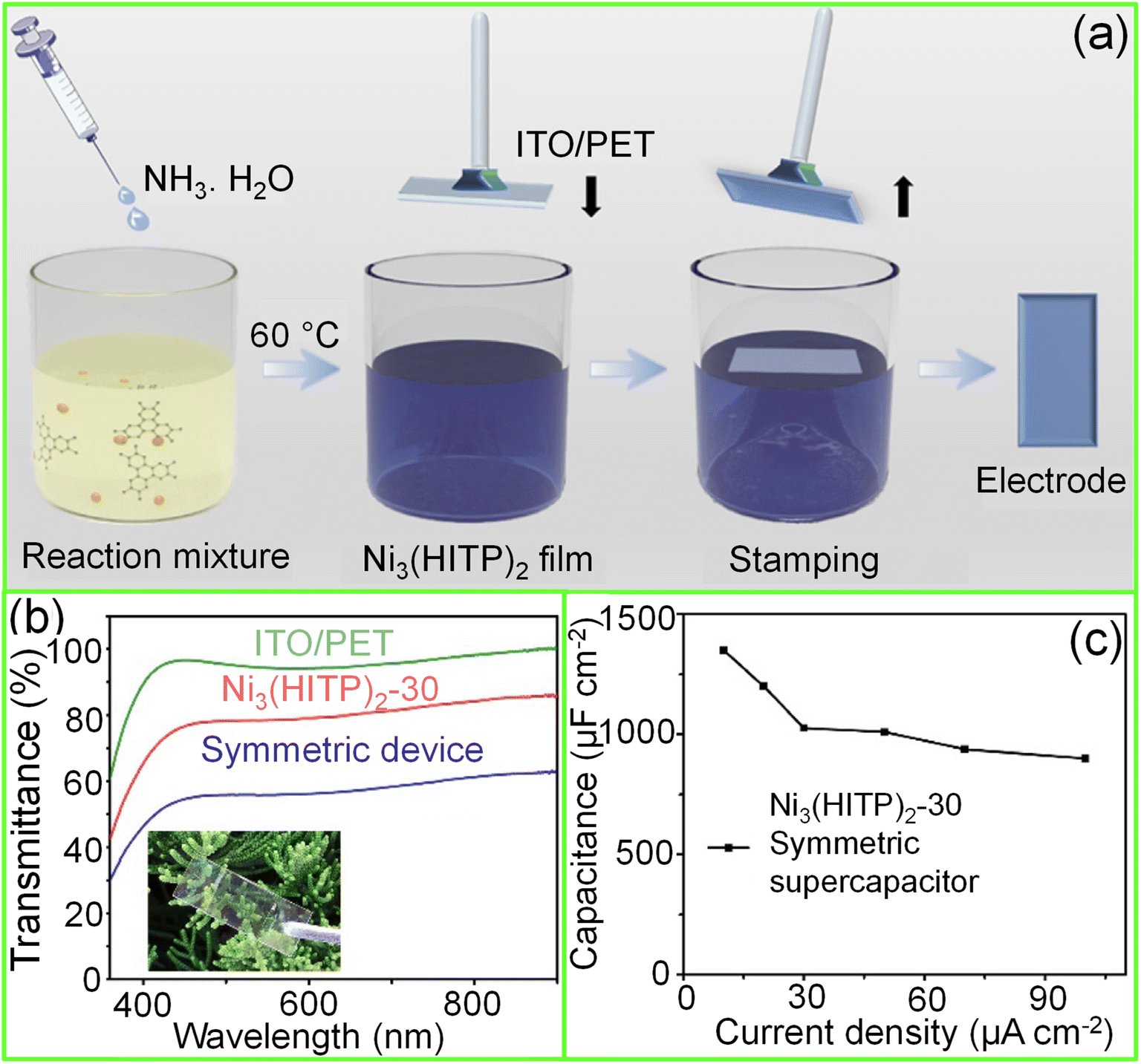 | ||
| Fig. 7 Metal–organic frameworks (MOFs): (a) schematic illustration of the fabrication of a Ni3(HITP)2 thin film over an ITO/PET substrate using the Langmuir–Schäfer method. (b) The transmittance spectra of the symmetric supercapacitor device compared with ITO/PET and Ni3(HITP)2-30 electrodes. Inset shows the photograph of the device. (c) The areal capacitance of the device plotted versus different current densities. Reprinted with permission from ref. 95. Copyright 2020 by Elsevier. | ||
2.2. Conducting networks
Unlike thin film conducting electrodes, network structures have designated conducting paths while the remaining regions transmit the incident light. Conducting network-based TCEs are broadly classified into non-template-based networks and template-based networks. The TCEs fabricated using a non-template-based approach are usually formed by brute force and therefore experience random conducting paths and cross-bar junctions. The electrical conductivity mainly occurs due to the percolative paths. In contrast, template-based networks are fabricated via the lithography approach, and thus the network remains in a plane without cross-bar junctions. However, template-based networks sometimes suffer from diffraction effects due to the orderliness of the network patterns.512.2.1.1. Metal nanowires. Achieving high transmittance and conductance with excellent stretchability in a capacitance device is extremely difficult, especially with thin conducting films, as there is a tradeoff between film thickness and conductivity. In the case of metal nanowires, by controlling the volume of nanowires and increasing the aspect ratio of nanowires, there is an improvement in the device's conductivity and transparency. Nanowire networks are sparely interconnected below a critical density (percolation threshold), and above this, the network conductivity increases drastically with an increase in the density of the nanowires. Therefore, conduction in metal nanowires is best described by percolation theory.49
Gong et al. fabricated a transparent supercapacitor using ultrathin gold nanowires (AuNWs), which are soft and serpentine-like at the nanoscale due to their ultrathin (diameter, 2 nm) and ultralong morphology (aspect ratio, >10000).96 Ultrathin AuNWs were synthesized by adding oleylamine (OA, 1.5 mL) to gold salt (HAuCl4·3H2O, 44 mg) in hexane (40 mL). The OA acts as a phase transfer reagent and helps in the complete dissolution of gold salt. After adding tri-isopropylsilane (TIPS, 2 mL), the solution was left to stand (2 days) without stirring until the solution changed from its initial yellow color to dark red, indicating the formation of AuNWs. The monolayer of AuNWs was achieved through a modified Langmuir–Blodgett technique. The AuNW-based all-solid-state (PVA/KNO3) transparent supercapacitor (79%) shows excellent stability towards stretching (up to 30%) due to its aligned wavy structures. The supercapacitor showed an areal specific capacitance of 226.8 μF cm−2 and a specific capacitance of 8.5 F g−1.96
In another example, AgNWs coated with vertically aligned Co(OH)2 are employed for supercapacitor fabrication as 2D-Co(OH)2 possesses high interlayer spacings and high theoretical capacitance (3460 F g−1) and low cost (see Fig. 8a).97 AgNW suspension was spin-coated on a PET substrate, followed by coating a ZnO precursor as a protective layer to prepare the electrodes. The zinc oxide precursor comprises zinc acetate dissolved in ethanol and diluted lactic acid is subsequently added until the solution becomes transparent and colorless. The Co(OH)2 nanosheets were electrochemically deposited on AgNWs using 0.01 M Co(NO3)2·6H2O with a static potential of −1.0 V versus the standard calomel electrode (SCE). After being washed with DI water, the Co(OH)2 nanosheets/AgNW hybrid electrodes were exposed to UV light (1 h) to enhance their stability. The transmittance of the hybrid electrode decreases with the increased deposition of Co(OH)2. The high areal capacitance (5.18 mF cm−2) was obtained at optimal loading of Co(OH)2 (5 minutes) with ∼75% transmittance (Fig. 8b). Also, this hybrid electrode retains 118% and 112% of initial areal capacitance after 10000 and 20000 charge–discharge cycles, respectively (Fig. 8c).97 The synergetic effect of Ag and Co(OH)2 nanosheets, the ZnO protecting layer, and UV irradiation treatments is the major reason for the outstanding cycling performance of the Co(OH)2 nanosheets/AgNW based supercapacitor device.97 Liu et al. have fabricated a transparent and flexible all-solid-state supercapacitor using ultra-long (∼75 μm) Ag nanowires which exhibit low sheet resistance (15.2 Ω sq−1) with high transmittance (84%). The fabricated all-solid-state flexible supercapacitor (PET/AgNWs/PEDOT:PSS/H3PO4/PVA/PEDOT:PSS/AgNWs/PET) with a PEDOT:PSS protective layer has shown ∼51% transmittance with a maximum areal capacitance of 0.9 mF cm−2 (device area ∼ 1 cm2) (see Fig. 8d and e).98 On the other hand, AgNWs and Ni/Co(OH)2 core–shell nanostructures fabricated by electrodeposition offer many advantages. It is interesting to note that a Ni–Co bimetal interface exists between AgNWs and Ni/Co(OH)2. This interface (Ag NW@NiCo/NiCo(OH)2) offers multiple advantages (Fig. 8f–h).99 The Ni–Co layer improves the electron transport at the interfaces and acts as an interlayer to decrease the lattice mismatch. It further slows down the expansion of the hydroxide shell upon repeated charge–discharge cycles. In addition, upon exposure to an alkaline environment, the Ni–Co interface converts to Ni/Co(OH)2, which helps increase the electrochemical performance. By properly tuning the ratio of Ni and Co, a high areal capacitance (22.2 mF cm−2) was achieved.99
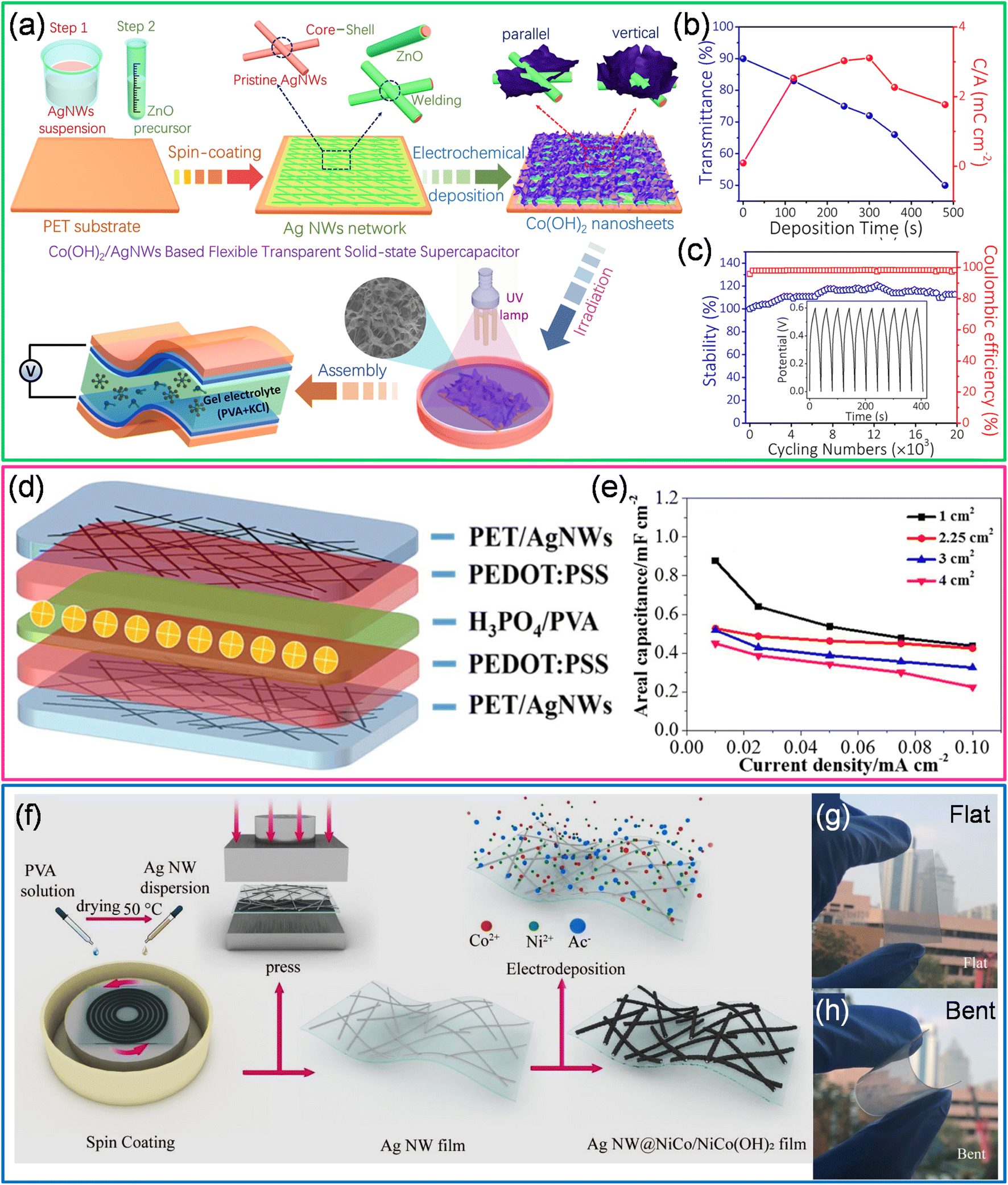 | ||
| Fig. 8 Metal nanowires: (a) schematic illustration of the fabrication of a transparent supercapacitor based on a Co(OH)2 nanosheets/Ag nanowire hybrid network. (b) The variation in optical transmittance and C/A with change in Co(OH)2 deposition times. (c) The stability and coulombic efficiency of the device versus the number of charge–discharge cycles. Reprinted with permission from ref. 97. Copyright 2019 American Chemical Society. (d) Schematic illustration of the fabrication of an all solid-state flexible supercapacitor with Ag NWs and PEDOT:PSS. (e) The areal capacitance was calculated from galvanostatic charge–discharge profiles for supercapacitors with various device areas. Reproduced with permission from ref. 98. Copyright 2018 American Chemical Society. (f) Schematic representation of fabrication of Ag NW@NiCo/NiCo(OH)2 electrodes. (g) and (h) Photographs of the electrode in flat and bent positions. Reproduced from ref. 99 with permission from the Royal Society of Chemistry. | ||
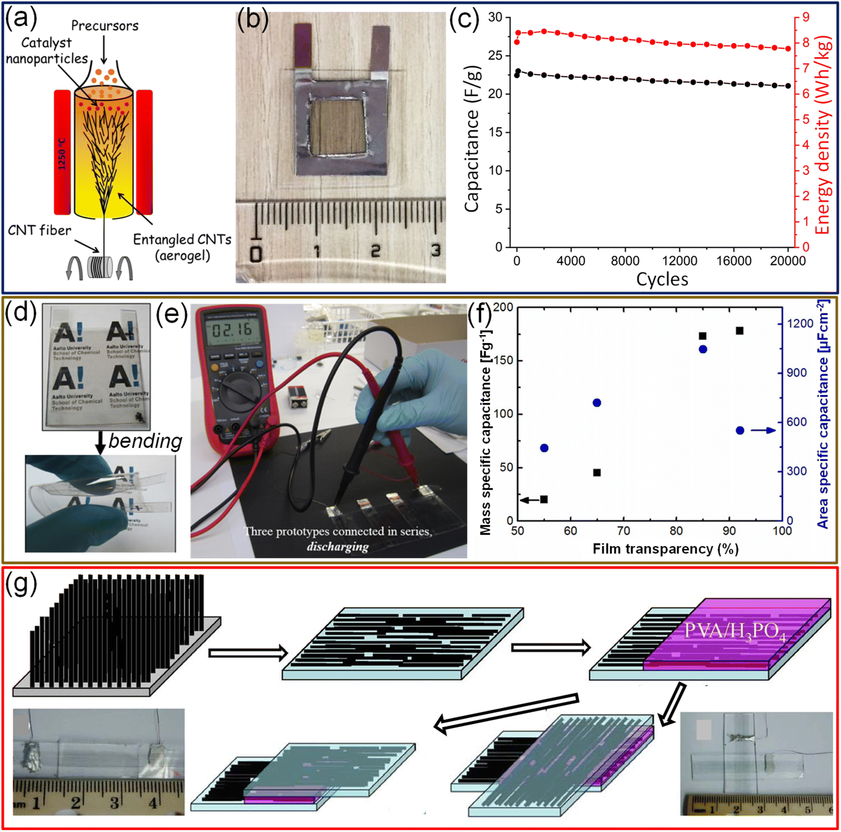
2.2.1.2. Carbon nanotubes (CNTs). Due to their excellent mechanical and electrical properties, besides natural abundance and low-cost, carbon nanotubes (CNTs) have been extensively used as alternative TCEs for many optoelectronic devices like touch screens,100 loudspeakers,101 and OLEDs.102 Among various synthesis methods, solution-based deposition is preferred for SWCNT-based TCE fabrication due to its low-cost and scalable approach. However, the solution-based approach suffers from aggregation and high-contact resistance due to the different molecules attached to the SWCNT surface. In this context, Zhiqiang Niu et al. prepared SWCNT-based TCEs using the floating catalyst chemical vapor deposition (FCCVD) technique followed by a “repeated halving” approach. The major drawback of the simple FCCVD technique is the high minimum thickness of the prepared CNT film (>100 nm).103 The repeated halving approach effectively reduces the thickness of the CNT film below 50 nm, improves the film's uniformity, and increases the utilization rate of SWCNTs. Transparent and symmetrical supercapacitors have been fabricated with such “repeated halving” CNTs on PET substrates (50 nm) which act both as an electrode and current collector, a transparent Nafion-117 membrane as a separator, and 1 M non-aqueous LiClO4 as the electrolyte. The fabricated device exhibits a specific capacitance of 22.5 F g−1 with about 60% transmittance at 550 nm.104 Similarly, CNTs prepared by the FCCVD technique were directly deposited onto both sides of the ionic liquid-based polymer electrolyte membrane, and the device showed high storage performance (Fig. 9a).105 The excellent electrical conductivity of the prepared CNTs precludes using an external current collector. The device exhibits high power density (1370 kW kg−1), high transmittance (70%) (Fig. 9b), and extraordinary electrochemical stability (94% capacitance retention over 20
000 cycles) (Fig. 9c).105 In another example, SWCNT thin films were deposited onto a polymer PDMS substrate via vacuum filtration with a subsequent stamping process. The optical transmittance of the SWCNT electrode decreases from 82% to 56% with increasing mass loading of SWCNTs (0.02–0.08 mg). To fabricate the supercapacitor, conducting carbon paste was used as an external current collector, SWCNTs as the electrode material, a Celgard-3401 as a separator, and TBAPF6 (tetrabutylammoniumhexa-fluorophosphate):PMMA (poly(methyl methacrylate)):PC (propylene carbonate):ACN (acetonitrile) in a ratio of 3:7:20:70 by weight as the electrolyte. The device fabricated with 0.02 mg SWCNT loading offers a specific capacitance of 22.2 F g−1 with about 82% transmittance.106 Prototype flexible EDLCs with SWCNTs prepared by aerosol CVD exhibit extremely high specific capacitance (178 F g−1 or 552 μF cm−2) with 90% transmittance and electrochemical stability for 10000 cycles (Fig. 9d–f).107 Chen et al. have demonstrated the fabrication of transparent (∼75%) and flexible supercapacitors using highly aligned CNTs on a PDMS polymer substrate (Fig. 9g). The device can be biaxially stretched up to 30% strain without changing the electrochemical performance.108
 | ||
| Fig. 9 Carbon nanotubes: (a) schematic representation of fabrication of CNT electrodes via the floating catalyst chemical vapor deposition technique. (b) Photograph of a free-standing transparent supercapacitor device. (c) The stability of the device tested for over 20000 charge–discharge cycles. Reproduced from ref. 105 with permission from the Royal Society of Chemistry. (d) Photographs of a transparent flexible supercapacitor device fabricated with SWCNT thin films. (e) Photograph of three proto-type devices connected in series while discharging. (f) The dependence of areal and mass-specific capacitance on the SWCNT thickness. © IOP Publishing Ltd. Reproduced with permission. All rights reserved.107 (g) Schematic diagram illustrating the fabrication process of a transparent and flexible supercapacitor using SWCNTs assembled in both parallel (bottom left) and cross (bottom right) configurations. Adapted with permission from ref. 108. Copyright 2014 by Springer Nature. | ||
Although SWCNTs are ideal for electrochemical double-layer capacitors (EDLCs) due to their high electrical conductance, chemical stability, and high surface area, the specific capacitance achievable with the EDLC mechanism is limited.109 In this context, coating a conducting polymer or metal oxides as an overlayer improves the specific capacitance via a pseudo-capacitor or redox supercapacitor mechanism. While preparing transparent supercapacitors, it is necessary to keep the thickness of the materials lower to achieve higher transmittance. However, the sheet resistance of a 15 nm thin SWCNT film is relatively high (1500 Ω sq−1). To fabricate SWCNT/PANI thin films on flexible substrates, SWCNT films were first transferred to a conducting FTO substrate, followed by electrodeposition of polyaniline. Finally, SWCNT/PANI films were transferred to flexible and transparent PET substrates (Fig. 10a). Compared to pristine SWCNTs and PANI, SWCNT/PANI composite films evidently show better electrochemical performance (see Fig. 10b). A supercapacitor fabricated with SWCNT (10.0 mg cm−2)/PANI (59 wt%) electrodes offers a specific capacitance of 55 F g−1 (Fig. 10c).109 Compared with the usage of only bare gel electrolytes between electrodes, the addition of monodispersed polystyrene microspheres helps control the spacing between electrolytes and protects the electrolyte from extrusion under deformation conditions (Fig. 10d and e).110 Furthermore, MWCNTs/MnO2 elevated the capacitance by at least an order of magnitude compared with SWCNTs.110 The specific capacitance of the aligned MWCNT/PANI electrodes is 36 times that of bare MWCNT electrodes, 23 times that of pure PANI and three times that of randomly oriented MWCNT/PANI electrodes.111
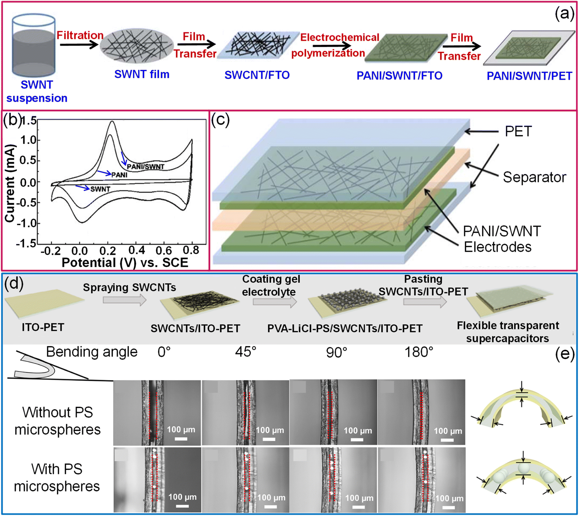 | ||
| Fig. 10 Carbon nanotubes: schematic illustrations of fabrication of a transparent hybrid PANI/SWCNT electrode (a). (b) The contrast of cyclic voltammograms of pristine SWCNT, PANI and hybrid PANI/SWCNT electrodes and the supercapacitor device (c). Reproduced from ref. 109 with permission from the Royal Society of Chemistry. (d) Schematic representation of fabrication of a flexible transparent supercapacitor using a PVA–LiCl–PS electrolyte and SWCNT/ITO hybrid electrodes. (e) Schematic diagram and cross-sectional SEM images illustrating the stability of the device with PS microspheres in the electrolyte while bending. Reproduced with permission from ref. 110. Copyright 2020 American Chemical Society. | ||
2.2.1.3. Electrospun fibers. Non-conventional template-based methods have emerged for fabricating random mesh-like network electrodes. Towards this end, the free-standing, continuous nanofiber webs of polymers are produced by electrospinning and used as sacrificial templates for fabricating transparent electrodes. Metal is either physically evaporated or chemically deposited by electroplating on top of the fibers that are selectively dissolved, resulting in hollow nanotrough type fully interconnected nanostructures. The nanotrough geometry is shown to be advantageous since the electromagnetic cross-section is smaller, allowing extra visible light to pass through the electrode. The fiber width, length, and density could be controlled by tuning the electrospinning conditions. Undoubtedly, an extremely high transmittance of ∼91% could be achieved at a very low RS value of ∼2 Ω sq−1.
Electrospun nanofiber networks coated with metal result in a highly conducting and transparent metal network. For instance, An et al. realized a TCE of 90% transmittance with 0.36 Ω sq−1 sheet resistance by combining electrospun and electroplating techniques.112 Besides offering excellent mechanical stability, the process is simple and eco-friendly.113 Similarly, a flexible transparent supercapacitor fabricated using a nanofiber composite (NFC) electrode (NiO@NFC//NiO@NFC) exhibited excellent mechanical flexibility (10000 bending cycles), high specific capacitance (160 F g−1), optical transmittance (∼75%) with maximum energy and power densities of 22 W h kg−1 and ∼500 W kg−1, respectively (Fig. 11a).113 While connecting two supercapacitor devices in either series or parallel, the output potential and current, respectively, were improved compared to single devices (Fig. 11b and c). The MnO2@Au NF network showed an areal capacitance of ∼2 mF cm−2 with ∼80% transmittance with a PVA/LiCl gel electrolyte.114 A freestanding Au-coated PVA network was obtained by electrospinning PVA followed by Au metal deposition. The highly porous MnO2 shell was electrodeposited under optimal conditions.114 Similarly, extremely long MnO2/Au stacked nanofiber networks on a PDMS substrate demonstrated a high areal capacitance (3.68 mF cm−2) with nearly 60% transmittance and exhibited stability towards various deformations.115 Besides simple oxides like MnO2, battery-type ternary nickel-cobalt sulfide (NiCoS) can also be coated on the metal nanofiber network. For instance, the Cu@Ni@NiCoS nanofiber network acts both as the positive and negative electrodes and, while sandwiched with a PVA/KOH gel electrolyte, yielding high volumetric power (248 μW cm−3) and energy densities (10.83 μW h cm−3) with 65% transmittance (Fig. 11d).116 In another example, an embedded PEDOT:PSS/AgNFs/NOA-63 hybrid transparent supercapacitor electrode was fabricated by a simple peel-off transfer technique that offered an areal capacitance of 0.91 mF cm−2 with ∼78% transmittance.70 The Ag deposited polymer nanofiber was initially transferred onto a PEDOT:PSS thin film and encapsulated with NOA-63. After UV curing, the PEDOT:PSS/AgNFs/NOA-63 film was carefully peeled off the Si substrate.70
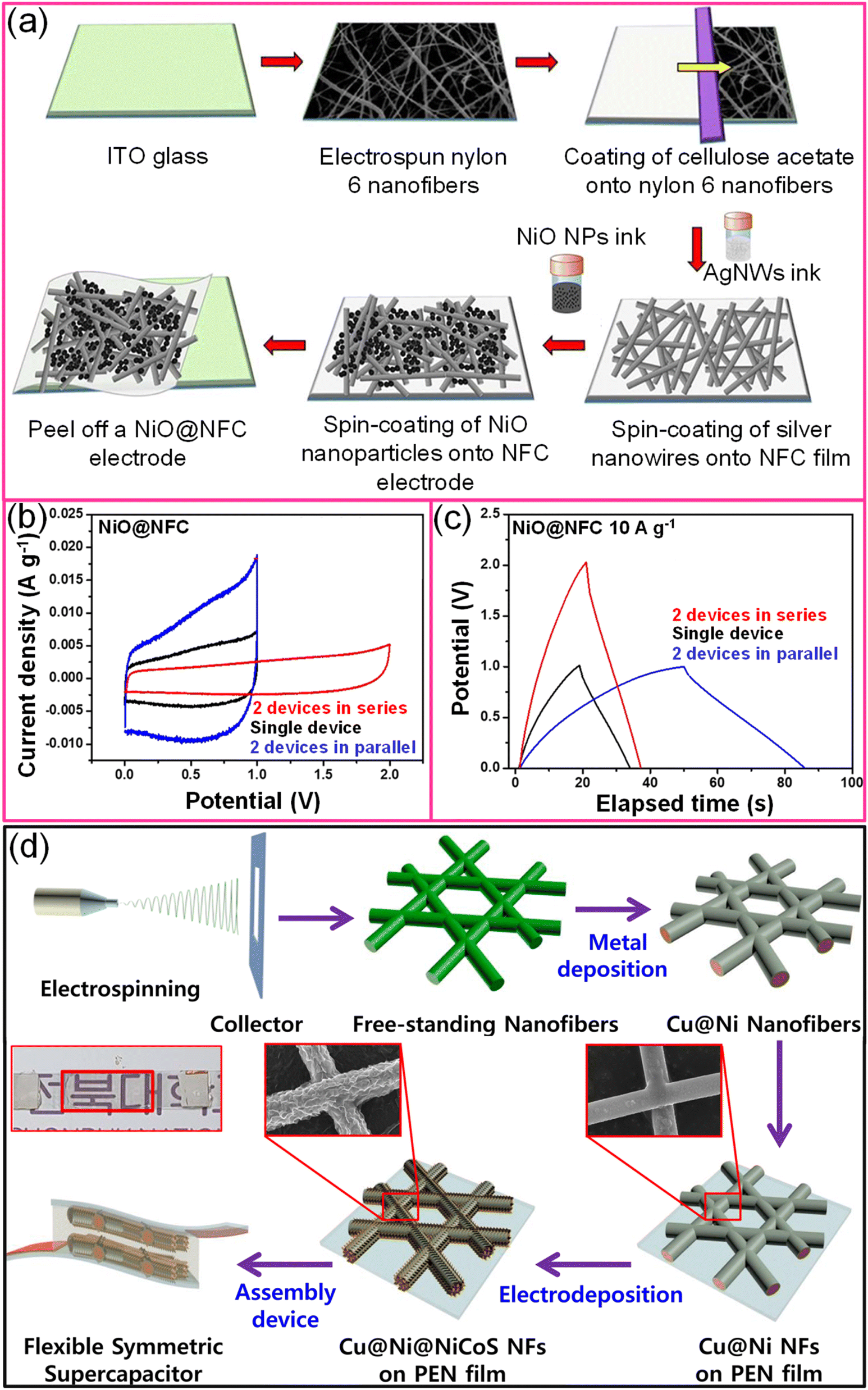 | ||
| Fig. 11 Electrospun fibers: (a) schematic representation to fabricate the NiO@nanofiber composite (NFC) based flexible and transparent symmetric supercapacitor device. (b) Cyclic voltammogram and (c) galvanostatic charge–discharge curves of a single NiO@NFC device and two devices connected in both series and parallel. Reproduced with permission from ref. 113. Copyright 2020 American Chemical Society. (d) Schematic illustration for the preparation of a transparent supercapacitor device using Cu@Ni@NiCoS nanofibers using the electrospinning technique. Reprinted with permission from ref. 116. Copyright 2020 by Elsevier. | ||
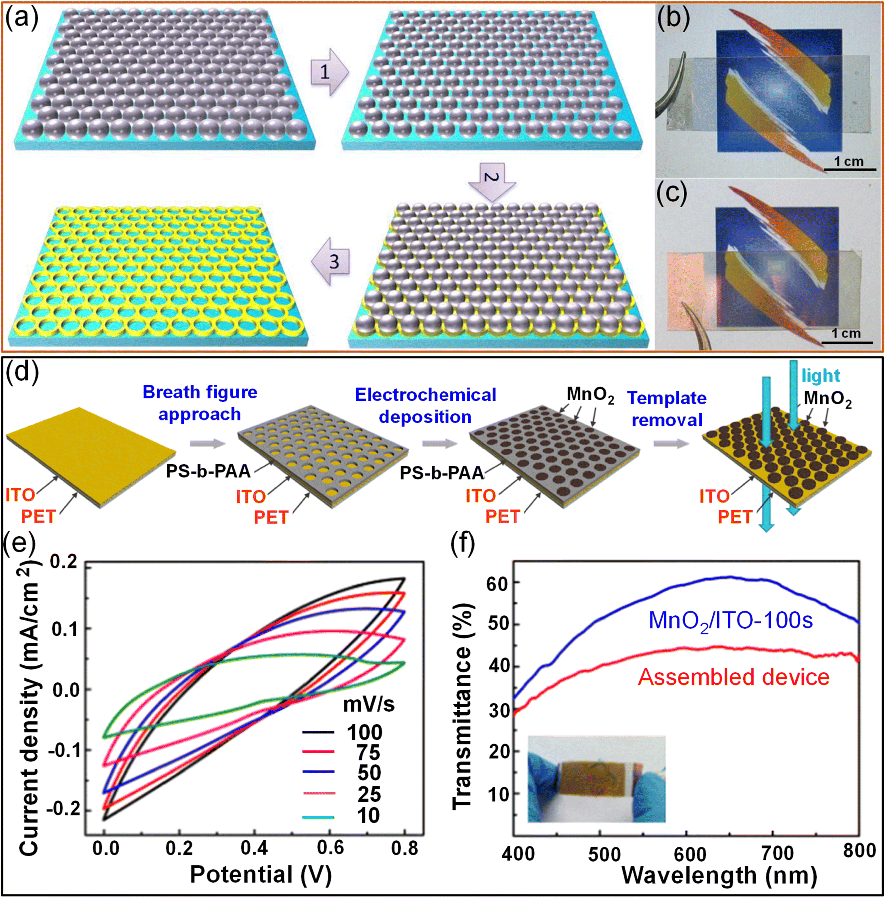
2.2.2.1. Lithography techniques. Nanosphere lithography is a popular technique for fabricating patterned structures due to its simplicity, low cost, and large throughput. A transparent supercapacitor with an Au@MnO2 core–shell structure was fabricated on a transparent flexible polymer substrate through nanosphere lithography and electrodeposition techniques. An Au mesh was developed on a PET substrate using a monolayer of hexagonally closely packed polystyrene spheres as a template, followed by reactive ion etching. Subsequently, the Au metal was deposited over the template, and polymer spheres were removed. The width of the Au mesh prepared on PET substrates entirely depends on the duration of ion etching. With increasing etching time, the resulting Au mesh width increases. Furthermore, electrodeposited MnO2 is conformally coated over the electrodeposited Au nanomesh. The interconnected Au mesh acts as a transparent conducting electrode and holds the pseudocapacitive MnO2 shell. The thickness of MnO2 increases with the electrodeposition time. Finally, an Au@MnO2 nanomesh-based transparent flexible supercapacitor was achieved by combining two such electrodes with a LiClO4/PVA gel electrolyte. The device exhibited an areal capacitance of ∼0.8 mF cm−2 with 40% transmittance (Fig. 12a–c).117 An Au nanomesh was also obtained using the grain boundary lithography approach, which involves a bilayer lift-off metallization process.118 The electrodeposited MnO2 shell offers a high surface area and thus enhances the capacitance without significantly altering the transmittance (84.7%). The imperceptible supercapacitor exhibits high areal capacitance (0.53 mF cm−2) with excellent stretchability and bending stability.45 In an example, MnO2 island-like arrays were fabricated by a breath-figure approach to fabricate a flexible transparent supercapacitor. Porous polystyrene-b-polyacrylic acid (PS-b-PAA) achieved by the breath-figure approach has been employed as a template for the MnO2 growth over ITO/PET via electrochemical deposition followed by removal of the PS-b-PAA template to realize MnO2 island arrays (Fig. 12d). The assembled MnO2/ITO/PET supercapacitor device exhibited typical supercapacitor like CV characteristics (Fig. 12e) and offers ∼5 mF cm−2 areal capacitance with an optical transmittance of 44% (Fig. 2f).119
 | ||
| Fig. 12 Lithography: (a) the synthetic procedure for preparing the Au nanomesh film through nanosphere lithography followed by reactive ion etching. Photographs of (b) the Au/PET film and (c) the Au@MnO2/PET film. Reproduced with permission from ref. 117. Copyright 2014 by John Wiley and Sons. (d) Schematic illustration of the fabrication of MnO2 island array electrodes using a breath-figure polymer pattern as a template for oxide growth. (e) CV curves of the fabricated supercapacitor device at various scan rates ranging from 10 to 100 mV s−1. (f) Transmittance spectra of the MnO2/ITO-100 s electrode and the assembled supercapacitor device (inset image). Reproduced with permission from ref. 119. Copyright 2018 American Chemical Society. | ||
In another approach, the patterned electrode grid, which occupies only a small fraction of the entire surface area, was developed using the soft lithography technique to offer high transparency to the supercapacitor device. While compared to other patterned electrodes, the transmittance of the full cell is significantly high due to the perfectly aligned electrodes. Highly transparent and flexible Ag/porous carbon or Ag/NixFeyOz@RGO electrodes featuring a hexagonal grid-like morphology were fabricated using a PDMS stamp prepared via photolithography. Initially, PDMS stamps and PET substrates were cleaned with O2 plasma to enhance the wettability of precursor inks. After pressing the stamps against PET substrates, precursor Ag ink was injected around the stamp's edges, and it flowed inside the mold by capillary force. The temperature was slowly increased to 130 °C to dry the precursor and to improve the conductivity of the Ag mesh. At this stage, the stamp is not filled with the Ag ink; thus, the active electrode precursor ink was injected around the stamp's edges. Finally, the PDMS stamp was carefully removed to realize Ag/porous carbon or Ag/NixFeyOz@RGO electrodes on transparent and flexible substrates. The Ag film exhibits ∼88% transmittance (7.6 Ω sq−1), which is further reduced to 85–86% due to the coating of carbon electrode materials. The areal capacitance and transmittance of the fully assembled supercapacitor device are 226.8 μF cm−2 and 70.6%, respectively.120
A freestanding, highly transparent (>84%), and conductive (3 × 10⁴ S cm−1) Ni network was obtained via a direct-write laser micro-patterning technique followed by selective electrodeposition. The thickness of the freestanding mesh can be tailored in the range of 1.5–5 μm by varying the electrodeposition duration. The MnO2 pseudocapacitive material was electrodeposited to increase the surface area of the electrode, which in turn increases the device's capacitance. The transparent Ni network can be attached to arbitrary objects such as pencils, leaves, and Rubik cubes. The electrochemical energy storage performance of the MnO2@Ni network electrode was examined using a PVA/LiCl gel electrolyte. The device achieved high transmittance (∼80%) and capacitance values (10.6 mF cm−2) due to MnO2 coating, besides offering superior flexibility.121 In another example, a Ni mesh/PEDOT:PSS hybrid was employed as the active electrode material for all-solid-state, flexible supercapacitors. The typical width and thickness of the metallic Ni ribbon are 3–5 μm and 0.8–3.5 μm, respectively. At the same time, the thickness can be precisely controlled by varying the deposition duration. The supercapacitor device showed ∼83% transmittance and high areal capacitance (0.52 mF cm−2) with excellent stability towards deformation.122 Xu et al. have fabricated an embedded Ag grid/PEDOT:PSS hybrid electrode by a facile soft UV imprinting lithography technique coupled with a scrap technique. Firstly, the direct laser writing technique patterned the photoresist layer into brick-wall grooves. Secondly, the patterned structure is transferred to a soft polyurethane acrylate mold and later to UV-curable resin via ultraviolet-nano-imprint lithography (UV-NIL). The UV-curable resin (D10, PhiChem) was cured by exposing it to UV light for just 2 s (1000 mW cm−2). Subsequently, Ag nanoparticle ink was drop cast on the UV resin layer, and nanoparticles were filled into grooves using the scrap technique, followed by annealing at 80 °C. Finally, the embedded Ag/PEDOT:PSS electrode was realized by spin-coating PEDOT:PSS solution onto Ag grid electrodes. A flexible transparent all-solid-state supercapacitor was obtained by pressing two Ag/PEDOT:PSS electrodes with a PVA/H3PO4 gel electrolyte. The fabricated supercapacitor offers high transmittance (∼80%) with high areal capacitance (2.79 mF cm−2) and retains around 92% of initial capacitance even after 10000 cycles of charging and discharging (Fig. 13a and b).41 Liu et al. fabricated a high-performance solid-state symmetric supercapacitor device (MnO2@Au–Ni mesh) with an areal capacitance of 78.5 mF cm−2 and an optical transmittance of 61%. In this process, self-standing hexagonal patterns of Ni were created by laser direct writing followed by selective electrodeposition of Ni. Further Au nanoparticles (nano-glue between Ni and MnO2) were electrodeposited, followed by MnO2 to realize transparent core–shell microstructures (see Fig. 13c–e). The electrode has shown an excellent areal capacitance of 1.15 F cm−2 (transmittance ∼ 70%).123
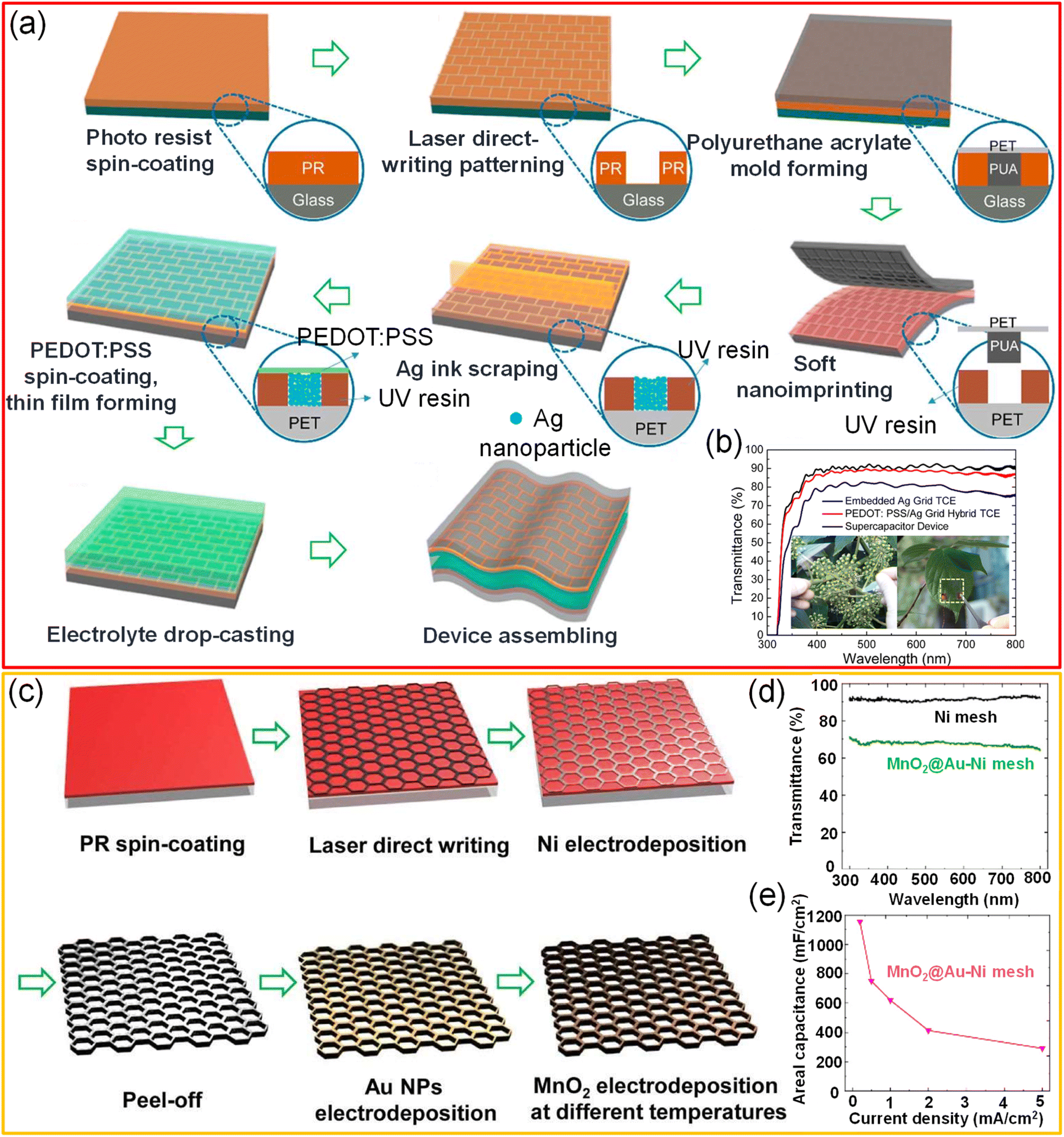 | ||
| Fig. 13 Lithography: (a) schematic representation of the fabrication of a flexible transparent solid-state supercapacitor using an embedded Ag grid TCE. (b) Transmittance spectra of the Ag grid TCE, the PEDOT:PSS/Ag grid hybrid TCE, and the supercapacitor device. Insets show the digital photographs of transparent supercapacitor devices prepared using the Ag grid TCE. Reproduced with permission from ref. 41. Copyright 2017 American Chemical Society. (c) Schematic illustration of fabricating a self-standing core–shell MnO2@Au–Ni mesh electrode. (d) Transmittance spectra of Ni mesh and MnO2@Au–Ni mesh electrodes. (e) The graph representing the relationship of areal capacitance with current density for the MnO2@Au–Ni mesh electrode. Reproduced with permission from ref. 123. Copyright 2019 American Chemical Society. | ||
Amidst multiple advantages, the biggest drawback associated with lithography-based techniques is the cost of the master, resist, and developer, along with the laborious processing steps. The nanoimprinting process requires a hard master, and a resist that is hard baked, followed by metal deposition. This has limited the use of lithography techniques in TCE fabrication. Another challenge is scalability since large contact areas between the mold and the imprinted nanostructures can result in sticking issues. Moreover, the pattern fidelity is compromised over large areas as the polymer chains in the active material tend to relax elastically. Most conventional lithography techniques are also unsuitable for directly fabricating nanostructures on flexible, curved, and rough surfaces.
2.2.2.2. Self-forming process. The choice of the templating method is crucial in determining the properties of the resulting transparent conducting electrode. A versatile approach based on a crack template was developed to fabricate a fully interconnected network. Interestingly, the method is termed a self-forming or spontaneously crackled template in parallel efforts from Han et al.124 and Kulkarni and coworkers,125–130 respectively. Both groups have demonstrated the fabrication of high-performance transparent electrodes by fine-tuning the control over the cracking process such that the metal network obtained after removing the sacrificial template is a fully interconnected network with a high transmittance of ∼85% and sheet resistance of ∼10 Ω sq−1. Meanwhile work carried out by Han et al. involved spin coating, which is restricted to the limited size of the substrate.124 Nevertheless, Kulkarni and co-workers demonstrated the formation of a crack template over a much wider length scale that can be fabricated on flat, flexible as well as curved surfaces and named it Crackle Lithography (CL).125–130 The scalability and uniformity of crackle templates over A4 size areas and even bigger are achieved by adopting several different coating processes, such as spray coating, roll coating, rod coating, drop coating etc. and are well established in the literature. Kiruthika et al. fabricated a transparent supercapacitor using the CL method in which highly interconnected spontaneously formed crackles were used as a template for electrode fabrication. Besides high interconnectivity among the crackles over a large area, crackles are down to the substrate and devoid of residual crackle precursors (acrylic resin).125 While depositing Au metal, the deposition occurs over the crackle template and inside cracks (i.e., substrate). After removing the template, an interconnected Au network with seamless junctions was achieved on the desired separator substrate. The transmittance and sheet resistance of the electrode could be fine-tuned by varying the width and density of the crackles and by the thickness of the metal, respectively. The electrochemically deposited MnO2@Au enhances the surface area and electrochemical capacitance. In place of sandwiching electrodes with a separator, the electrodes were developed on both sides of the separator substrate, resulting in a lightweight supercapacitor. The device exhibited high areal capacitance (3.2 mF cm−2) and transmittance (78%) with excellent cycling stability, as shown in Fig. 14.125 In another study, transparent MoS2@Ni and MnO2@Ni mesh-based transparent asymmetric supercapacitors were fabricated on a plastic substrate via the crackle template approach (silica template). A maximum areal capacitance of 2.42 mF cm−2 with ∼50% transmittance with excellent mechanical stability was achieved.131 Metal-based hybrid TCEs have shown superior performance and attracted worldwide attention.132,133 Commonly used metals Ag, Au and Cu have mainly been utilized to fabricate transparent electrodes due to their high electrical conductivity, availability, and ease of processing.
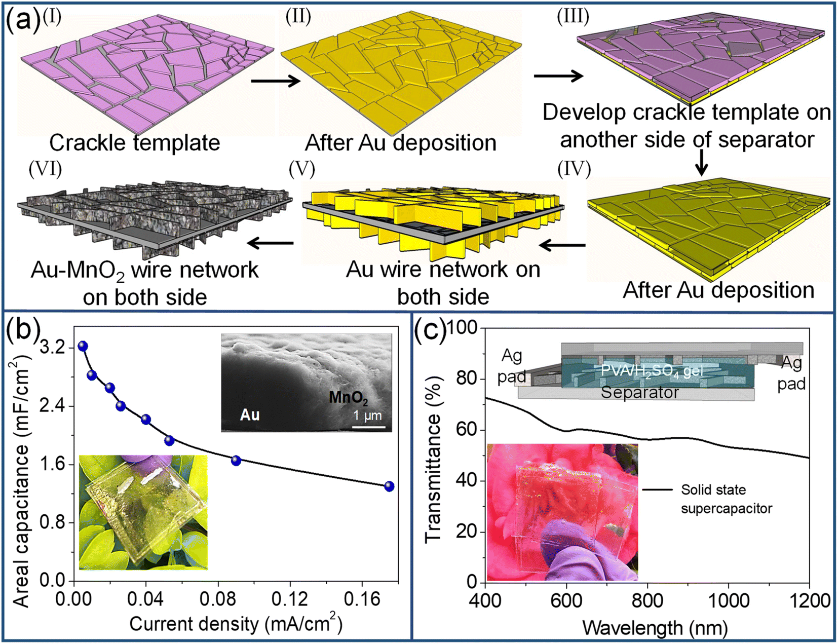 | ||
| Fig. 14 Self-forming process: (a) schematic representation to fabricate a core–shell Au/MnO2 network using a crackle template. (b) A graph showing the areal capacitance of the Au/MnO2 supercapacitor electrode versus its discharging current densities. The insets in (b) show the SEM images of the fabricated Au/MnO2 nanowire mesh and the device's photograph. (c) The solid-state supercapacitor of the Au/MnO2 electrode device (bottom) shows a transmittance of 78%, and the inset shows a schematic of a solid-state supercapacitor device. Reproduced with permission from ref. 125. Copyright 2017 by John Wiley and Sons. | ||
3. Flexible transparent micro-supercapacitors
From basic research and practical applications, lightweight and flexible micro-energy storage devices that can be integrated into circuits have become more crucial to meet the requirements of flexible, multifunctional, and wearable electronics.134 The micro-supercapacitor (MSC) device aims to avoid heavy packaging, improve transparency and facilitate integration in portable electronics. Sollami Delekta et al. developed graphene-based interdigitated electrodes for flexible transparent MSCs via inkjet printing. 7-layer graphene interdigital electrodes with a 600 μm width, 2.5 mm length, and 200 μm spacings were coated with a PVA/H3PO4 gel electrolyte for flexible transparent supercapacitors. The device offers high transmittance (87%) with excellent bending stability (91.3%) with a maximum areal capacitance of 12.6 μF cm−2.135 To fabricate MSCs with more inherent mechanical flexibility, high-rate capacity, and cycling stability, Li et al. employed AgNWs–MoS2 based hybrid interdigitated electrodes with a width and interspacing of 1000 and 25 μm, respectively, using a direct laser writing approach. The fabricated in-plane micro-supercapacitors demonstrated ∼77.5% transmittance with high specific areal capacitance (27.6 mF cm−2) and retained 96.4% capacitance even after 10000 charge–discharge cycles.136 Yu and coworkers created carbon nanoparticles/Ni-based micro-supercapacitors by depositing carbon nanoparticles on a finger-type Ni current collector. Finally, the devices were assembled using gel electrolytes, yielding a capacitance of 2.89 F g−1 with nearly 45% transmittance. Because of their outstanding performance, the fabricated device can be used in flexible electronics.4,137 Direct write methods, including inkjet printing and laser ablation of conducting films, have been developed as alternative high throughput, low-cost methods.138 Some of them are even adaptable to large-area processing. In any case, a micro-supercapacitor has the option to attain higher capacitance by stacking up along the third dimension laterally while maintaining a desired value of transmittance. Still, the printed features are much wider, of the order of tens and hundreds of microns, which obstructs the visibility and deteriorates the current collection efficiency of electrodes. These are usually integrated with ultrathin films of metal, ITO, graphene, or PEDOT:PSS as hybrid electrodes for improved charge storage properties.138 However, if a continuous thin film is grown thick laterally, the charge storage sites beneath the top layers may become inaccessible by the ions, thus increasing the resistance and limiting the capacitance.25 Nevertheless, a junction-free, fully interconnected network in the form of an aperiodic mesh is highly advantageous. Table 1 summarizes the optical and electrochemical performances of various transparent supercapacitors discussed so far.
| Electrode material for transparent supercapacitors | Active materials | Electrolyte | Transmittance | Capacitance | Energy density | Power density | Ref. | |
|---|---|---|---|---|---|---|---|---|
| a Transparent micro-supercapacitor (TMSC), nanoparticle (NP), tricarballylicacid (TC), nanowires (NW), and nanofibers (NF). | ||||||||
| Ultra-thin conducting networks | Graphene | Ultrathin graphene films | 2 M KCl | 70% (550 nm) | 135 F g−1 | 15.4 W h kg−1 | 554 W kg−1 | 55 |
| CVD-grown graphene bilayers and redox-active interlayer | PVA/H2SO4 | 75% (550 nm) | 101 μF cm−2 | ∼0.02 W h cm−3 | 90 W cm−3 | 57 | ||
| Graphene sheets via rapid thermal annealing (RTA) | PVA/H3PO4 | ∼67% (500–800 nm) | 12.4 μF cm−2 | 2.94 W h kg−1 | 438.6 kW kg−1 | 63 | ||
| Free-standing flexible graphene paper grown using NaCl as a template | PVA/H2SO4 | 59% (800 nm) | 3.3 mF cm−2 | 430 μW h cm−3 | 190 mW cm−3 | 42 | ||
| Single layer graphene via thermal CVD | Polyacrylonitrile electrospun mat soaked in PVA–LiCl | ∼59% (550 nm) | 3.83 μF cm−2 | — | — | 141 | ||
| Organic thin films | Free-standing PEDOT:PSS via facile multilayer spin-coating | PVA/H3PO4 | ∼60% (550 nm) | ∼4.72 mF cm−2 | 0.38 mW h cm−2 | 0.036 W cm−2 | 68 | |
| PEDOT: PSS in formic acid | 0.5 M K2SO4 (aq.) | 70% (550 nm) | 1.9 mF cm−2 | — | — | 25 | ||
| Polypyrrole | H3PO4/PVA | 71% (550 nm) | 1.64 mF cm−2 | 5 mW h cm−3 | 67.3 mW h cm−3 | 40 | ||
| Metal oxides | ITO | 1-Butyl-3-methylimidazolium chloride and cellulose | 92% (450–800 nm) | ∼18 F g−1 | — | — | 77 | |
| ITO/Co3O4 | PVA/H3PO4 | 51% (550 nm) | 6.03 mF cm−2 | 3.01 W h kg−1 | 1.152 kW kg−1 | 78 | ||
| ITO/MnO2 | 1 M Na2SO4 | 77.4% (550 nm) | 9.2 mF cm−2 | — | — | 80 | ||
| MnO NP/TC/ITO NP/TC | 0.5 M Na2SO4 | 60.8% (550 nm) | 40.5 mF cm−2 | 0.82 μW h cm−2 | 113 μW cm−2 | 81 | ||
| Coaxial RuO2-ITO nanopillars | 0.5 M H2SO4 | ∼60% (550 nm) | 1235 F g−1 | — | — | 82 | ||
| AZO/NiO | PVA/KOH | 83% (550 nm) | 3.4 mF cm−2 | 45.38 nW h cm−2 | 4.97 μW cm−2 | 85 | ||
| MoO3 nano-paper | PVA/LiCl | ∼90% (400–800 nm) | ∼258 F g−1 | 22.89 W h kg−1 | 10.1 kW kg−1 | 86 | ||
| MXenes | Ti3C2Tx | PVA/H2SO4 | ∼80% (550 nm) | 0.86 mF cm−2 | 0.011 μW h cm−2 | 0.62 μW cm−2 | 39 | |
| MOFs | Ni3(HITP)2 | PVA/KCl | 55.8% (550 nm) | 1.35 mF cm−2 | 0.05 μW h cm−2 | 1.25 μW cm−2 | 95 | |
| Non-template based | Metal nanowires | AuNWs | PVA/KNO3 and PVA/H3PO4 | 79% (550 nm) | 226.8 μF cm−2 | — | — | 96 |
| Carbon nano-tubes | SWCNT | 1 M LiClO4 | 60% (550 nm) | 22.5 F g−1 | 12.5 W h kg−1 | 13.9 kW kg−1 | 104 | |
| CNT fibre aerogels | (Pyr14TFSI):(PVDF-co-HFP) | 70% (550 nm) | 29 F g−1 | 10 W h kg−1 | 1370 kW kg−1 | 105 | ||
| SWCNT | TBAPF6:PMMA:PC:ACN | 82% (550 nm) | 34.2 F g−1 | 18 kW h kg−1 | 21.1 kW kg−1 | 106 | ||
| SWCNT | PVA/H3PO4 | 92% (550 nm) | 552 μF cm−2 | — | — | 107 | ||
| CNT/PDMS | PVA/H3PO4 | ∼75% (550 nm) | 7.3 F g−1 | 1 W h kg−1 | 1.1 kW kg−1 | 108 | ||
| SWCNT/PANI | 1 M H2SO4 | 70% (550 nm) | 55 F g−1 | — | — | 109 | ||
| MWCNTs/MnO2 | PVA/LiCl | 52.3% (550 nm) | 1.7 mF cm−2 | — | — | 110 | ||
| MWCNT/PANI | H3PO4/PVA | 70% (300–900 nm) | 233 F g−1 | — | — | 111 | ||
| Electrospun fibers | MnO2@Au nanofibers | PVA/LiCl | ∼80% (400–800 nm) | ∼2 mF cm−2 | 0.14 μW h cm−2 | 4 μW cm−2 | 114 | |
| MnO2/Au nanofiber networks | LiClO4/PVA | 60% (550 nm) | 3.68 mF cm−2 | 56 μW h cm−2 | 0.32 μW cm−2 | 115 | ||
| Cu@Ni@NiCoS | PVA/KOH | 65% (550 nm) | 1.21 μA h cm−2 | 10.83 μW h cm−3 | 248 μW cm−3 | 116 | ||
| Template based | Lithography | Au@MnO2 core–shell | LiClO4/PVA | 40% (550 nm) | ∼0.8 mF cm−2 | — | — | 117 |
| Au@MnO2 nanomesh electrodes | PVA/Na2SO4 | 82% (550 nm) | 0.53 mF cm−2 | 0.047 μW h cm−2 | 2.16 μW cm−2 | 45 | ||
| MnO2@Ni network | PVA/LiCl | ∼80% (550 nm) | 10.6 mF cm−2 | — | — | 121 | ||
| MnO2/ITO/PET | PVA/LiCl | 44% (550 nm) | 4.73 mF cm−2 | — | — | 119 | ||
| MnO2@Au–Ni mesh | PVA/LiCl | 61.1% (550 nm) | 78.46 mF cm−2 | — | — | 123 | ||
| Self-forming | MnO2@Au | 1 M Na2SO4 | ∼75% (550 nm) | 3.2 mF cm−2 | ∼2 mW h cm−3 | ∼2 W cm−3 | 125 | |
| MoS2@Ni and MnO2@Ni | LiCl/PVA | ∼50% (550 nm) | 2.42 mF cm−2 | ∼0.86 μW h cm−2 | 16 μW cm−2 | 131 | ||
| Hybrid | Tungsten oxide nanoflakes/nitrogen doped graphene quantum dots | PVA/H3PO4 | 70% (400–800 nm) | 178.82 F g−1 | 15.8 W h kg−1 | 360.1 W kg−1 | 62 | |
| Graphene/CNTs/AgNW | PVA/H3PO4 | 64% (550 nm) | ∼0.31 mF cm−2 | 25.5 nW h cm−2 | 1.25 μW cm−2 | 56 | ||
| AgNWs/Ni(OH)2–PEIE/PEDOT:PSS | PVA/LiCl | 80% (550 nm) | 3.3 mF cm−2 | 0.074 μW h cm−2 | 3.2 μW cm−2 | 69 | ||
| PEDOT:PSS/AgNFs/NOA 63 | H2SO4/PVA | 77.4% (550 nm) | 0.91 mF cm−2 | 2.31 mW h cm−3 | 0.13 W cm−3 | 70 | ||
| Ag/Au/polypyrrole | PVA/H3PO4 | 73% (550 nm) | 580 μF cm−2 | ∼10 W h kg−1 | ∼1000 W kg−1 | 76 | ||
| Au/graphene composites | PVA/H3PO4 | ∼75% (520 nm) | ∼82 μF cm−2 | — | — | 61 | ||
| ITO/PEDOT | PVP/LiClO4 | ∼50% (370–770 nm) | 15 F g−1 | — | — | 83 | ||
| In2O3 nanowires and CNT composites | 1 M LiClO4 | ∼65% (550 nm) | 64 F g−1 | 1.29 W h kg−1 | 7.48 kW kg−1 | 84 | ||
| SWCNT and Ti3C2Tx TCEs | PVA/H2SO4 | 72% (550 nm) | 1.6 mF cm−2 | 0.05 μW h cm−2 | 2.4 μW cm−2 | 39 | ||
| Ni3(HITP)2//PEDOT:PSS | PVA/KCl | 61% (550 nm) | 1.06 mF cm−2 | 0.12 μW h cm−2 | 1.35 μW cm−2 | 95 | ||
| Co(OH)2 nano-sheets/Ag nanowires | PVA/PAAS/KCl | 54% (550 nm) | 5.18 mF cm−2 | 0.04 μW h cm−2 | 28.8 μW cm−2 | 97 | ||
| PET/AgNWs/PEDOT:PSS/H3PO4/PVA/PEDOT:PSS/AgNWs/PET | H3PO4/PVA | ∼51% (550 nm) | 0.273 mF cm−2 | ∼1.5 W h kg−1 | ∼300 W kg−1 | 98 | ||
| Ag NW@NiCo/NiCo(OH)2 | PVA/LiClO4/KOH | 54.3% (550 nm) | 22.2 mF cm−2 | 3.0 W h kg−1 | 3.5 W kg−1 | 99 | ||
| Ni mesh/PEDOT:PSS | PVA/H3PO4 | ∼83% (550 nm) | 0.52 mF cm−2 | — | — | 122 | ||
| Ag grid/PEDOT:PSS | PVA/H3PO4 | ∼80% (550 nm) | 2.79 mF cm−2 | — | — | 41 | ||
| Ag/porous carbon and Ag/NixFeyOz@reduced graphene oxide | PVDF–HFP/LiTFSI | 70.6% (550 nm) | 226.4 μF cm−2 | 2.7 mW h L−1 | 1002.5 mW h L−1 | 120 | ||
| MnO2/CNT | [BMIM][TFSI]/PMMA | ∼80% (550 nm) | 12.6 mF cm−2 | 0.04 μW h cm−2 | 7.94 μW cm−2 | 143 | ||
| PANI@ITO and PANI/CNT | PVA/H2SO4 | — | 140 F g−1 | — | — | 147 | ||
| AgNW/PEDOT:PSS/PU | PVA/H3PO4 | ∼75% (550 nm) | 190 μF cm−2 | — | — | 142 | ||
| Flexible TMSC | Graphene via inkjet printing technology | PVA/H3PO4 | 87% (550 nm) | 12.6 μF cm−2 | — | — | 135 | |
| Ag nanowires and MoS2 nanosheets | PVA/H2SO4 | ∼77.5% (550 nm) | 27.6 mF cm−2 | 2.453 μW h cm−2 | 1.472 mW cm−2 | 136 | ||
| Carbon NPs/Ni-based micro-supercapacitor | 1 M Et4NBF4/propylene carbonate | 45% (400–1100 nm) | 2.89 F g−1 | — | — | 137 | ||
4. Applications of transparent supercapacitors
Transparent supercapacitors find enormous applications combined with solar cells and other functional devices.92,139,140 For instance, Chun et al. fabricated self-charging power and touch-sensing systems using single-layer graphene-based electrodes (Fig. 15a).141 The schematic on the right shows that the top panel performs a dual role of behaving as a supercapacitor and a touch sensor whereas the bottom panel behaves as triboelectric nanogenerators (TENGs). These two devices are coupled using a rectifying bridge circuit to realize all-in-one self-charging power systems (Fig. 15a). The TENG device converts mechanical motions into electrical energy and stores it in rapidly charging supercapacitor devices. The stored energy can be later utilized for driving any wearable and portable electronic gadgets or sensors without any external power supplies. Fig. 15b shows the voltage versus time curve of the TENG device for various applied forces and frequencies and further compares the performance with that of reference ITO electrodes. The device exhibits excellent performance with low charge leakage while loading and unloading the forces in repeated cycles.141 The integration of an ultra-low-power-consuming strain sensor with a supercapacitor and TENG device resulted in a self-powered strain monitoring system.142 The active material for fabricating all three functional devices is AgNWs/PEDOT:PSS/PU. Fig. 15c shows an electrical circuit diagram integrating the strain sensor with SC and TENG devices. The transparency of the device is evident from the photograph shown in Fig. 15d. The device is useful in monitoring a wide range of human skin strains, including breathing and coughing (Fig. 15e and f).142 In another example, a skin attachable strain sensor (SS) is integrated with a flexible transparent micro-supercapacitor (MSC) which possesses a fractal structure to ensure high stretchability.143 The carbon nanotubes coated with MnO2 in combination with a 1-butyl-3-methylimidazoliumbis(trifluoromethylsulfonyl)imide/poly(methyl methacrylate) electrolyte serve as an electrode for MSCs (Fig. 15g). The fabricated MSC offers ∼80% transmittance with 12.6 mF cm−2 areal capacitance (see Fig. 15h). Interestingly, the change in the resistance of an AgNW based SS device while monitoring the pulse rate gives the same values when tested using a constant applied voltage (0.8 V) or with a MSC.143 Due to the possible switching between completely transparent and dark-colored states, integrating electrochromic properties with energy storage in a single device is made possible, allowing fine control of light and heat through the window while simultaneously powering any low-power household electronics. Researchers have also designed electrochromic supercapacitors that provide an optical indicator of the charge stored in a supercapacitor by optical modulation from a fully charged colored state to a discharged transparent state.144–146 An electrochromic supercapacitor shows various colors during the charging and discharging process and finds numerous applications such as displays, energy-saving smart windows, etc. The conducting polyaniline, an organic polymer, is a more common material used for this purpose because of its simple synthesis, cost-effectiveness, stability, and so on.144 Cho et al. fabricated an energy-storing functional photovoltaic device that can harvest solar energies and store it as electrical energy (see the circuit diagram in Fig. 15i).139 This multifunctional energy system is developed by monolithically integrating semi-transparent OPVs with electrochromic supercapacitors. The stored electrical energy can be a power source for various electronic gadgets like LEDs, sensors, etc. The image illustrates the operation of a red LED (1.8 V) using the energy stored in functional photovoltaics (Fig. 15i). The usage of an active electrochromic material helps by visually guiding the level of energy stored.139 In another instance, conducting polyaniline polymers in combination with CNTs/ITO have been used for demonstrating the self-charging behavior of supercapacitors while illuminated with a light source (Fig. 15j and k). More importantly, this photo-charging effect of the supercapacitor occurs with no external bias.147 In another report, a transparent supercapacitor is integrated with transparent electrodes to develop wirelessly rechargeable skin heat patches. Fig. 15l schematically shows the integration of a supercapacitor with an antenna, a diode, and capacitors to introduce wireless operation in the device. Fig. 15m illustrates the circuit diagram of the heat patch. On charging, the switch remains open and the AC power applied is rectified to DC power. In contrast, when discharging occurs, the switch is closed, and the stored energy from the supercapacitor is directed to the antenna to produce heat. The system remains robust for multiple cycles of charging and discharging.148 Furthermore, a schematic diagram clearly showing the vital requirements of transparent supercapacitors for integrating in various transparent devices is shown in Fig. 16. The electrochromic transparent supercapacitors that exhibit complete transparent and dark states are rarely observed in the literature, and such devices can be very crucial for energy-efficient windows for specifically controlling the light and heat as an added functionality.149,150 Presently, many electrochromic materials exhibit either a blue or a green color and are not completely transparent in the bleached state, thus restricting the complete advantage in window applications where transparency is necessary for visual appeal. | ||
| Fig. 15 Applications of transparent supercapacitors. (a) A rectifying-bridge circuit diagram integrating an energy harvesting triboelectric nanogenerator (TENG) with an energy-saving supercapacitor fabricated using single-layer graphene (SLG) electrodes. (b) The charging voltage vs. time curve for various applied frequencies (0.5 and 2 Hz) and forces (17 and 51 kPa) towards the TENG device to charge the supercapacitor. The ITO-based capacitor was used as the reference. Reproduced with permission from ref. 141. Copyright 2019 American Chemical Society. (c) The electrical circuit diagram shows the integration of the strain sensor with the supercapacitor and TENG devices using a rectifier. The AgNW/PEDOT:PSS/PU nanocomposite was employed as an active material for the fabrication of all three devices. (d) Photograph illustrating the transparency of the fabricated strain sensor attached to the neck. (e) and (f) Resistance variation for the strain sensor upon breathing and coughing, respectively, measured using a supercapacitor charged by a TENG. Reproduced with permission from ref. 142. Copyright 2015 American Chemical Society. (g) The cross-sectional view of a transparent and stretchable energy storage micro-supercapacitor (MSC) device for driving an integrated strain sensor (SS) and (h) its photograph. Reprinted with permission from ref. 143. Copyright 2020 by Elsevier. (i) The electrical circuit diagram of semitransparent energy storing functional photovoltaics (energy harvesting) connected with an electrochromic supercapacitor (energy storing) (top). The pictures shown in the bottom correspond to glowing red LED light using the energy stored by the supercapacitor through photovoltaics upon illumination. Reproduced with permission from ref. 139. Copyright 2020 by John Wiley and Sons. (j) Schematic representation of the fabrication of a polymer supercapacitor capable of self-charging under sunlight. (k) The variation in current density with time while illuminating the device with AM 1.5 solar illumination (power density ∼ 1000 W m−2) (red line) and under no illumination (blue line) without any external voltage bias. Reproduced with permission from ref. 147. Copyright 2015 American Chemical Society. (l) Schematic illustrating the integration of a supercapacitor with rectifiers and antennas. The photograph on the right is a transparent flexible, and wirelessly rechargeable heat patch. The scale bar corresponds to 1 cm. (m) Schematic representation denoting the change in the circuit diagram of the heat patch while under wirelessly charging and discharging cycles. Reproduced with permission from ref. 148. Copyright 2020 American Chemical Society. | ||
 | ||
| Fig. 16 Schematic representation highlighting the requirement of transparent supercapacitors as an energy storage device for various flexible transparent devices. Strain sensor – the photograph of a self-powered strain sensor composed of an AgNW/PEDOT:PSS/PU nanocomposite integrated with a supercapacitor, and a triboelectric nanogenerator. Reproduced with permission from ref. 142. Copyright 2015 American Chemical Society. Thermal therapy – a photograph of a transparent, flexible CuZr NTs–AgNW based hybrid supercapacitor for thermal therapy. Reproduced with permission from ref. 148. Copyright 2020 American Chemical Society. Photo-charging – the photograph of a transparent PANI/CNT polymer supercapacitor for photo-charging applications. Reproduced with permission from ref. 147. Copyright 2015 American Chemical Society. Touch sensor – a photograph of a single-layer graphene-based multifunctional supercapacitor device for self-charging and touch sensing. Reproduced with permission from ref. 141. Copyright 2019 American Chemical Society. Electrochromic – picture depicting the operation of four heart shaped totally independent energy-storing photovoltaics integrated with electrochromic supercapacitors under AM 1.5 G light. Reproduced with permission from ref. 139. Copyright 2020 by John Wiley and Sons. | ||
5. Closing remarks and future prospects
Due to enormous research activities, transparent electrodes for energy storage devices have been successfully developed over the last two decades. Supercapacitors are vital among many energy storage systems because of their excellent performance. Under persistent efforts, many electrode materials like graphene, CNTs, organic thin films, metal oxides, MXenes, MOFs, and metal nanowire networks, including hybrid electrodes, have been explored even with new device designs and configurations. However, desirable transparency and electrochemical performance with low-cost materials and methods for large-scale production challenge the practical application of transparent supercapacitors. Due to the existing trade-off between transmittance and capacitance, novel approaches are being developed to achieve high transparency (>90%) with high capacitance for modern transparent electronics. Instead of conventional device configurations, 3D-printed supercapacitors are gaining attention. Furthermore, modification approaches like developing electrodes on both sides of the separator substrate not only increase transmittance but also reduce the usage of unessential components. The requirement/specification of transmittance and desired capacitance usually depends on the application. For example, in the case of a transparent display, the desired transparency is usually aimed at ∼90%, and the capacitance is optimized accordingly with an appropriate choice of electrode material. However, for applications such as large-area smart windows with electrochromic properties, the transmittance can be compromised up to ∼70% while augmenting the areal-specific capacitance. The transparent supercapacitor is integrated with an electrochromic display, and the optical modulation serves as an indicator for the charging–discharging of the supercapacitor. Despite many significant developments, the status of transparent supercapacitors still needs to catch up to the practical commercial applications in transparent electronics. Besides transparency, accomplishing multiple functionalities like flexibility, stretchability, and self-healable properties is in demand. Finally, it is realized that continuous efforts are needed to improve the performance and introduce special functions in transparent energy storage devices for futuristic multifunctional transparent wearable electronic gadgets.Conflicts of interest
There are no conflicts to declare.Acknowledgements
The authors dedicate this article to Professor Giridhar U. Kulkarni, JNCASR, Bangalore. S. K. acknowledges the funding from SERB POWER Grant (SPG/2020/000442) and SIRE Grant (SIRE/2022/000524). N. S. acknowledges SERB POWER Grant for her fellowship. S. K. and N. S. acknowledge SASTRA Deemed University for their infrastructural support and encouragement. R. G. acknowledges the funding from SERB (SIRE/2022/000380) and Women Excellence Award (WEA/2020/000038).References
- L. Wang and X. Hu, Batteries Supercaps, 2020, 3, 1275–1286 CrossRef CAS.
- R. G. Gordon, MRS Bull., 2000, 25, 52–57 CrossRef CAS.
- M. Mativenga, D. Geng, B. Kim and J. Jang, ACS Appl. Mater. Interfaces, 2015, 7, 1578–1585 CrossRef CAS PubMed.
- W. Zhao, M. Jiang, W. Wang, S. Liu, W. Huang and Q. Zhao, Adv. Funct. Mater., 2021, 31, 2009136 CrossRef CAS.
- J. Jiang, B. Bao, M. Li, J. Sun, C. Zhang, Y. Li, F. Li, X. Yao and Y. Song, Adv. Mater., 2016, 28, 1420–1426 CrossRef CAS.
- D. Khim, G. S. Ryu, W. T. Park, H. Kim, M. Lee and Y. Y. Noh, Adv. Mater., 2016, 28, 2752–2759 CrossRef CAS PubMed.
- C. Zou, A. Komar, S. Fasold, J. Bohn, A. A. Muravsky, A. A. Murauski, T. Pertsch, D. N. Neshev and I. Staude, ACS Photonics, 2019, 6, 1533–1540 CrossRef CAS.
- J. Chen, Y. Wang, W. Liu and Y. Ma, ChemNanoMat, 2020, 6, 42–52 CrossRef CAS.
- J. Li, Q. Jiang, N. Yuan and J. Tang, Materials, 2018, 11, 2280 CrossRef.
- E. Navarrete-Astorga, J. Rodríguez-Moreno, E. A. Dalchiele, R. Schrebler, P. Leyton, J. R. Ramos-Barrado and F. Martín, J. Solid State Electrochem., 2017, 21, 1431–1444 CrossRef CAS.
- P. Simon and Y. Gogotsi, Nat. Mater., 2008, 7, 845–854 CrossRef CAS.
- J. R. Miller and P. Simon, Science, 2008, 321, 651–652 CrossRef CAS.
- Y. Z. Zhang, Y. Wang, T. Cheng, L. Q. Yao, X. Li, W. Y. Lai and W. Huang, Chem. Soc. Rev., 2019, 48, 3229–3264 RSC.
- W. K. Chee, H. N. Lim, Z. Zainal, N. M. Huang, I. Harrison and Y. Andou, J. Phys. Chem. C, 2016, 120, 4153–4172 CrossRef CAS.
- H. Guo, Y. J. Tan, G. Chen, Z. Wang, G. J. Susanto, H. H. See, Z. Yang, Z. W. Lim, L. Yang and B. C. K. Tee, Nat. Commun., 2020, 11, 5747 CrossRef CAS PubMed.
- Y. Lee, J. Park, A. Choe, S. Cho, J. Kim and H. Ko, Adv. Funct. Mater., 2020, 30, 1904523 CrossRef CAS.
- P. Wang, M. Hu, H. Wang, Z. Chen, Y. Feng, J. Wang, W. Ling and Y. Huang, Adv. Sci., 2020, 7, 2001116 CrossRef CAS.
- Q. Liu, Z. Liu, C. Li, K. Xie, P. Zhu, B. Shao, J. Zhang, J. Yang, J. Zhang, Q. Wang and C. F. Guo, Adv. Sci., 2020, 7, 2000348 CrossRef CAS.
- Y. Gu, T. Zhang, H. Chen, F. Wang, Y. Pu, C. Gao and S. Li, Nanoscale Res. Lett., 2019, 14, 263 CrossRef PubMed.
- D. Zhao, Y. Zhu, W. Cheng, W. Chen, Y. Wu and H. Yu, Adv. Mater., 2020, 33, 2000619 CrossRef PubMed.
- N. Kurra, S. Kiruthika and G. U. Kulkarni, RSC Adv., 2014, 4, 20281–20289 RSC.
- Z. Fan, IOP Conf. Ser.: Mater. Sci. Eng., 2020, 772, 012107 CrossRef CAS.
- S. Palchoudhury, K. Ramasamy, R. K. Gupta and A. Gupta, Front. Mater., 2019, 5, 83 CrossRef.
- C. (John) Zhang, T. M. Higgins, S. H. Park, S. E. O'Brien, D. Long, J. N. Coleman and V. Nicolosi, Nano Energy, 2016, 28, 495–505 CrossRef.
- T. M. Higgins and J. N. Coleman, ACS Appl. Mater. Interfaces, 2015, 7, 16495–16506 CrossRef CAS.
- A. M. Smith and S. Nie, Acc. Chem. Res., 2010, 43, 190–200 CrossRef CAS PubMed.
- G. Bahuguna, P. Ram, R. K. Sharma and R. Gupta, ChemElectroChem, 2018, 5, 2767–2773 CrossRef CAS.
- R. Gupta, K. D. M. Rao, S. Kiruthika and G. U. Kulkarni, ACS Appl. Mater. Interfaces, 2016, 8, 12559–12575 CrossRef CAS PubMed.
- G. Bahuguna, S. Chaudhary, R. K. Sharma and R. Gupta, Energy Technol., 2019, 7, 1900667 CrossRef CAS.
- A. B. Urgunde, G. Bahuguna, A. Dhamija, P. P. Das and R. Gupta, ACS Appl. Electron. Mater., 2020, 2, 3178–3186 CrossRef CAS.
- R. Gupta and T. S. Fisher, Energy Technol., 2016, 5, 740–746 CrossRef.
- J. Pu, X. Wang, R. Xu, S. Xu and K. Komvopoulos, Microsyst. Nanoeng., 2018, 4, 16 CrossRef PubMed.
- J. R. Gribbin, Q Is for Quantum: An Encyclopedia of Particle Physics, New York, Touchstone, 2000 Search PubMed.
- A. M. Ganose and D. O. Scanlon, J. Mater. Chem. C, 2016, 4, 1467–1475 RSC.
- G. Brunin, F. Ricci, V. A. Ha, G. M. Rignanese and G. Hautier, npj Comput. Mater., 2019, 5, 63 CrossRef.
- P. J. King, T. M. Higgins, S. De, N. Nicoloso and J. N. Coleman, ACS Nano, 2012, 6, 1732–1741 CrossRef CAS PubMed.
- C. (John) Zhang and V. Nicolosi, Energy Storage Mater., 2019, 16, 102–125 CrossRef.
- R. M. Mutiso, M. C. Sherrott, A. R. Rathmell, B. J. Wiley and K. I. Winey, ACS Nano, 2013, 7, 7654–7663 CrossRef CAS PubMed.
- C. J. Zhang, B. Anasori, A. Seral-Ascaso, S. H. Park, N. McEvoy, A. Shmeliov, G. S. Duesberg, J. N. Coleman, Y. Gogotsi and V. Nicolosi, Adv. Mater., 2017, 29, 1702678 CrossRef PubMed.
- X. Jiao, C. Zhang and Z. Yuan, ACS Appl. Mater. Interfaces, 2018, 10, 41299–41311 CrossRef CAS.
- J. L. Xu, Y. H. Liu, X. Gao, Y. Sun, S. Shen, X. Cai, L. Chen and S. D. Wang, ACS Appl. Mater. Interfaces, 2017, 9, 27649–27656 CrossRef CAS.
- N. Li, G. Yang, Y. Sun, H. Song, H. Cui, G. Yang and C. Wang, Nano Lett., 2015, 15, 3195–3203 CrossRef CAS.
- Y. Chen, J. Ma, M. Xu and S. Liu, Nano Today, 2020, 35, 100976 CrossRef CAS PubMed.
- H. Lee, S. Hong, J. Lee, Y. D. Suh, J. Kwon, H. Moon, H. Kim, J. Yeo and S. H. Ko, ACS Appl. Mater. Interfaces, 2016, 8, 15449–15458 CrossRef CAS.
- J. Yang, T. Hong, J. Deng, Y. Wang, F. Lei, J. Zhang, B. Yu, Z. Wu, X. Zhang and C. F. Guo, Chem. Commun., 2019, 55, 13737–13740 RSC.
- S. Bellani, L. Najafi, G. Tullii, A. Ansaldo, R. Oropesa-Nuñez, M. Prato, M. Colombo, M. R. Antognazza and F. Bonaccorso, J. Mater. Chem. A, 2017, 5, 25177–25186 RSC.
- T. G. Yun, M. Park, D. H. Kim, D. Kim, J. Y. Cheong, J. G. Bae, S. M. Han and I. D. Kim, ACS Nano, 2019, 13, 3141–3150 CrossRef CAS.
- A. Kumar and C. Zhou, ACS Nano, 2010, 4, 11–14 CrossRef CAS PubMed.
- G. U. Kulkarni, S. Kiruthika, R. Gupta and K. D. M. Rao, Curr. Opin. Chem. Eng., 2015, 8, 60–68 CrossRef.
- S. R. C. Vivekchand, R. Chandra Sekhar, A. Govindaraj and C. N. R. Rao, J. Chem. Sci., 2008, 120, 9–13 CrossRef CAS.
- K. S. Novoselov, A. K. Geim, S. V. Morozov, D. Jiang, Y. Zhang, S. V. Dubonos, I. V. Grigorieva and A. A. Firsov, Science, 2004, 306, 666–669 CrossRef CAS.
- K. S. Novoselov, V. I. Fal'Ko, L. Colombo, P. R. Gellert, M. G. Schwab and K. Kim, Nature, 2012, 490, 192–200 CrossRef CAS PubMed.
- J. Xia, F. Chen, J. Li and N. Tao, Nat. Nanotechnol., 2009, 4, 505–509 CrossRef CAS PubMed.
- S. Guo and S. Dong, Chem. Soc. Rev., 2011, 40, 2644–2672 RSC.
- A. Yu, I. Roes, A. Davies and Z. Chen, Appl. Phys. Lett., 2010, 96, 253105 CrossRef.
- H. Peng, Y. Zhong, X. Zhang, Y. He and G. Wang, Langmuir, 2018, 34, 15245–15252 CrossRef CAS.
- K. Jo, S. Lee, S. M. Kim, J. Bin In, S. M. Lee, J. H. Kim, H. J. Lee and K. S. Kim, Chem. Mater., 2015, 27, 3621–3627 CrossRef CAS.
- E. O. Polat and C. Kocabas, Nano Lett., 2013, 13, 5851–5857 CrossRef CAS PubMed.
- X. Fan, T. Chen and L. Dai, RSC Adv., 2014, 4, 36996–37002 RSC.
- P. Xu, J. Kang, J. B. Choi, J. Suhr, J. Yu, F. Li, J. H. Byun, B. S. Kim and T. W. Chou, ACS Nano, 2014, 8, 9437–9445 CrossRef CAS PubMed.
- Y. Chen, X. Y. Fu, Y. Y. Yue, N. Zhang, J. Feng and H. B. Sun, Appl. Surf. Sci., 2019, 467–468, 104–111 CrossRef CAS.
- Q. A. Sial, M. S. Javed, Y. J. Lee, L. T. Duy and H. Seo, Ceram. Int., 2020, 46, 23145–23154 CrossRef CAS.
- Y. Gao, Y. S. Zhou, W. Xiong, L. J. Jiang, M. Mahjouri- Samani, P. Thirugnanam, X. Huang, M. M. Wang, L. Jiang and Y. F. Lu, APL Mater., 2013, 1, 012101 CrossRef.
- M. Z. Rahman and T. Edvinsson, J. Mater. Chem. A, 2020, 8, 8234–8237 RSC.
- J. Cárdenas-Martínez, B. L. España-Sánchez, R. Esparza and J. A. Ávila-Niño, Synth. Met., 2020, 267, 116436 CrossRef.
- L. V. Kayser and D. J. Lipomi, Adv. Mater., 2019, 31, 1806133 CrossRef PubMed.
- H. Yan and H. Okuzaki, Synth. Met., 2009, 159, 2225–2228 CrossRef CAS.
- T. Cheng, Y. Z. Zhang, J. P. Yi, L. Yang, J. D. Zhang, W. Y. Lai and W. Huang, J. Mater. Chem. A, 2016, 4, 13754–13763 RSC.
- R. T. Ginting, M. M. Ovhal and J. W. Kang, Nano Energy, 2018, 53, 650–657 CrossRef CAS.
- S. B. Singh, T. Kshetri, T. I. Singh, N. H. Kim and J. H. Lee, Chem. Eng. J., 2019, 359, 197–207 CrossRef CAS.
- J. Xu, D. Wang, L. Fan, Y. Yuan, W. Wei, R. Liu, S. Gu and W. Xu, Org. Electron., 2015, 26, 292–299 CrossRef CAS.
- W. Xiong, X. Hu, X. Wu, Y. Zeng, B. Wang, G. He and Z. Zhu, J. Mater. Chem. A, 2015, 3, 17209–17216 RSC.
- Y. Hu, Y. Zhao, Y. Li, H. Li, H. Shao and L. Qu, Electrochim. Acta, 2012, 66, 279–286 CrossRef CAS.
- Y. Huang, H. Li, Z. Wang, M. Zhu, Z. Pei, Q. Xue, Y. Huang and C. Zhi, Nano Energy, 2016, 22, 422–438 CrossRef CAS.
- I. Shown, A. Ganguly, L. C. Chen and K. H. Chen, Energy Sci. Eng., 2015, 3, 2–26 CrossRef CAS.
- H. Moon, H. Lee, J. Kwon, Y. D. Suh, D. K. Kim, I. Ha, J. Yeo, S. Hong and S. H. Ko, Sci. Rep., 2017, 7, 41981 CrossRef CAS PubMed.
- D. Wei, S. J. Wakeham, T. W. Ng, M. J. Thwaites, H. Brown and P. Beecher, Electrochem. Commun., 2009, 11, 2285–2287 CrossRef CAS.
- X. Y. Liu, Y. Q. Gao and G. W. Yang, Nanoscale, 2016, 8, 4227–4235 RSC.
- F. Moser, L. Athouël, O. Crosnier, F. Favier, D. Bélanger and T. Brousse, Electrochem. Commun., 2009, 11, 1259–1261 CrossRef CAS.
- Y. Hu, H. Zhu, J. Wang and Z. Chen, J. Alloys Compd., 2011, 509, 10234–10240 CrossRef CAS.
- J. Choi, D. Nam, D. Shin, Y. Song, C. H. Kwon, I. Cho, S. W. Lee and J. Cho, ACS Nano, 2019, 13, 12719–12731 CrossRef CAS PubMed.
- I. Ryu, M. Yang, H. Kwon, H. K. Park, Y. R. Do, S. B. Lee and S. Yim, Langmuir, 2014, 30, 1704–1709 CrossRef CAS.
- J. Rodríguez, E. Navarrete, E. A. Dalchiele, L. Sánchez, J. R. Ramos-Barrado and F. Martín, J. Power Sources, 2013, 237, 270–276 CrossRef.
- P. C. Chen, G. Shen, S. Sukcharoenchoke and C. Zhou, Appl. Phys. Lett., 2009, 94, 043113 CrossRef.
- V. Q. Le, P. A. Le, S. C. Wu, Y. H. Lai, Y. G. Lin, K. H. Wei, Y. H. Chu and Y. L. Chueh, Small, 2020, 16, 2000020 CrossRef CAS.
- B. Yao, L. Huang, J. Zhang, X. Gao, J. Wu, Y. Cheng, X. Xiao, B. Wang, Y. Li and J. Zhou, Adv. Mater., 2016, 28, 6353–6358 CrossRef CAS.
- M. W. Barsoum, Prog. Solid State Chem., 2000, 28, 201–281 CrossRef CAS.
- M. Naguib, M. Kurtoglu, V. Presser, J. Lu, J. Niu, M. Heon, L. Hultman, Y. Gogotsi and M. W. Barsoum, Adv. Mater., 2011, 23, 4248–4253 CrossRef CAS PubMed.
- P. Salles, E. Quain, N. Kurra, A. Sarycheva and Y. Gogotsi, Small, 2018, 14, 1802864 CrossRef PubMed.
- J. Halim, M. R. Lukatskaya, K. M. Cook, J. Lu, C. R. Smith, L. Å. Näslund, S. J. May, L. Hultman, Y. Gogotsi, P. Eklund and M. W. Barsoum, Chem. Mater., 2014, 26, 2374–2381 CrossRef CAS PubMed.
- K. Hantanasirisakul, M. Q. Zhao, P. Urbankowski, J. Halim, B. Anasori, S. Kota, C. E. Ren, M. W. Barsoum and Y. Gogotsi, Adv. Electron. Mater., 2016, 2, 1600050 CrossRef.
- L. Qin, J. Jiang, Q. Tao, C. Wang, I. Persson, M. Fahlman, P. O. A. Persson, L. Hou, J. Rosen and F. Zhang, J. Mater. Chem. A, 2020, 8, 5467–5475 RSC.
- G. Wu, J. Huang, Y. Zang, J. He and G. Xu, J. Am. Chem. Soc., 2017, 139, 1360–1363 CrossRef CAS PubMed.
- D. Sheberla, L. Sun, M. A. Blood-forsythe, S. Er, C. R. Wade and C. K. Brozek, J. Am. Chem. Soc., 2014, 136, 8859 CrossRef CAS PubMed.
- W. Zhao, T. Chen, W. Wang, B. Jin, J. Peng, S. Bi, M. Jiang, S. Liu, Q. Zhao and W. Huang, Sci. Bull., 2020, 65, 1803–1811 CrossRef CAS PubMed.
- S. Gong, Y. Zhao, Q. Shi, Y. Wang, L. W. Yap and W. Cheng, Electroanalysis, 2016, 28, 1298–1304 CrossRef CAS.
- H. Sheng, X. Zhang, Y. Ma, P. Wang, J. Zhou, Q. Su, W. Lan, E. Xie and C. J. Zhang, ACS Appl. Mater. Interfaces, 2019, 11, 8992–9001 CrossRef CAS.
- X. Liu, D. Li, X. Chen, W. Y. Lai and W. Huang, ACS Appl. Mater. Interfaces, 2018, 10, 32536–32542 CrossRef CAS PubMed.
- J. Liu, G. Shen, S. Zhao, X. He, C. Zhang, T. Jiang, J. Jiang and B. Chen, J. Mater. Chem. A, 2019, 7, 8184–8193 RSC.
- H.-Z. Geng, K. K. Kim, K. P. So, Y. S. Lee, Y. Chang and Y. H. Lee, J. Am. Chem. Soc., 2007, 129, 7758–7759 CrossRef CAS PubMed.
- L. Xiao, Z. Chen, C. Feng, L. Liu, Z. Q. Bai, Y. Wang, L. Qian, Y. Zhang, Q. Li, K. Jiang and S. Fan, Nano Lett., 2008, 8, 4539–4545 CrossRef CAS PubMed.
- D. Zhang, K. Ryu, X. Liu, E. Polikarpov, M. Tompson and C. Zhou, Nano Lett., 2006, 6, 1880–1886 CrossRef CAS PubMed.
- W. Ma, L. Song, R. Yang, T. Zhang, Y. Zhao, L. Sun, Y. Ren, D. Liu, L. Liu, J. Shen, Z. Zhang, Y. Xiang, W. Zhou and S. S. Xie, Nano Lett., 2007, 7, 2307–2311 CrossRef CAS PubMed.
- Z. Niu, W. Zhou, J. Chen, G. Feng, H. Li, Y. Hu, W. Ma, H. Dong, J. Li and S. Xie, Small, 2013, 9, 518–524 CrossRef CAS PubMed.
- E. Senokos, M. Rana, M. Vila, J. Fernandez-Cestau, R. D. Costa, R. Marcilla and J. J. Vilatela, Nanoscale, 2020, 12, 16980–16986 RSC.
- R. Yuksel, Z. Sarioba, A. Cirpan, P. Hiralal and H. E. Unalan, ACS Appl. Mater. Interfaces, 2014, 6, 15434–15439 CrossRef CAS PubMed.
- P. Kanninen, N. D. Luong, L. H. Sinh, I. V. Anoshkin, A. Tsapenko, J. Seppälä, A. G. Nasibulin and T. Kallio, Nanotechnology, 2016, 27, 235403 CrossRef PubMed.
- T. Chen, H. Peng, M. Durstock and L. Dai, Sci. Rep., 2014, 4, 1–7 Search PubMed.
- J. Ge, G. Cheng and L. Chen, Nanoscale, 2011, 3, 3084–3088 RSC.
- J. Chen, W. Xiao, T. Hu, P. Chen, T. Lan, P. Li, Y. Li, B. Mi and Y. Ma, ACS Appl. Mater. Interfaces, 2020, 12, 5885–5891 CrossRef CAS PubMed.
- H. Lin, L. Li, J. Ren, Z. Cai, L. Qiu, Z. Yang and H. Peng, Sci. Rep., 2013, 3, 1353 CrossRef PubMed.
- S. An, H. S. Jo, D. Y. Kim, H. J. Lee, B. K. Ju, S. S. Al-Deyab, J. H. Ahn, Y. Qin, M. T. Swihart, A. L. Yarin and S. S. Yoon, Adv. Mater., 2016, 28, 7149–7154 CrossRef CAS PubMed.
- C. S. Kwak, T. H. Ko, J. H. Lee, H. Y. Kim and B. S. Kim, ACS Appl. Energy Mater., 2020, 3, 2394–2403 CrossRef CAS.
- S. B. Singh, T. I. Singh, N. H. Kim and J. H. Lee, J. Mater. Chem. A, 2019, 7, 10672–10683 RSC.
- Y. Lee, S. Chae, H. Park, J. Kim and S. H. Jeong, Chem. Eng. J., 2020, 382, 122798 CrossRef CAS.
- B. S. Soram, I. S. Thangjam, J. Y. Dai, T. Kshetri, N. H. Kim and J. H. Lee, Chem. Eng. J., 2020, 395, 125019 CrossRef CAS.
- T. Qiu, B. Luo, M. Giersig, E. M. Akinoglu, L. Hao, X. Wang, L. Shi, M. Jin and L. Zhi, Small, 2014, 10, 4136–4141 CAS.
- C. F. Guo, T. Sun, Q. Liu, Z. Suo and Z. Ren, Nat. Commun., 2014, 5, 3121 CrossRef PubMed.
- Y. Wang, W. Zhou, Q. Kang, J. Chen, Y. Li, X. Feng, D. Wang, Y. Ma and W. Huang, ACS Appl. Mater. Interfaces, 2018, 10, 27001–27008 CrossRef CAS PubMed.
- T. Liu, R. Yan, H. Huang, L. Pan, X. Cao, A. deMellollo and M. Niederberger, Adv. Funct. Mater., 2020, 30, 2004410 CrossRef CAS.
- Y. H. Liu, J. L. Xu, X. Gao, Y. L. Sun, J. J. Lv, S. Shen, L. Sen Chen and S. D. Wang, Energy Environ. Sci., 2017, 10, 2534–2543 RSC.
- Y. H. Liu, J. L. Xu, S. Shen, X. L. Cai, L. Sen Chen and S. D. Wang, J. Mater. Chem. A, 2017, 5, 9032–9041 RSC.
- Y. H. Liu, Z. Y. Jiang and J. L. Xu, ACS Appl. Mater. Interfaces, 2019, 11, 24047–24056 CrossRef CAS.
- B. Han, K. Pei, Y. Huang, X. Zhang, Q. Rong, Q. Lin, Y. Guo, T. Sun, C. Guo, D. Carnahan, M. Giersig, Y. Wang, J. Gao, Z. Ren and K. Kempa, Adv. Mater., 2014, 26, 873–877 CrossRef CAS PubMed.
- S. Kiruthika, C. Sow and G. U. Kulkarni, Small, 2017, 13, 1701906 CrossRef.
- S. Kiruthika, R. Gupta, A. Anand, A. Kumar and G. U. Kulkarni, ACS Appl. Mater. Interfaces, 2015, 7, 27215–27222 CrossRef CAS.
- S. Kiruthika, R. Gupta and G. U. Kulkarni, RSC Adv., 2014, 4, 49745–49751 RSC.
- R. Gupta, K. D. M. Rao, K. Srivastava, A. Kumar, S. Kiruthika and G. U. Kulkarni, ACS Appl. Mater. Interfaces, 2014, 6, 13688–13696 CrossRef CAS.
- S. Kiruthika, R. Gupta, K. D. M. Rao, S. Chakraborty, N. Padmavathy and G. U. Kulkarni, J. Mater. Chem. C, 2014, 2, 2089–2094 RSC.
- R. Gupta, K. D. M. Rao and G. U. Kulkarni, RSC Adv., 2014, 4, 31108–31112 RSC.
- B. S. Soram, J. Y. Dai, I. S. Thangjam, N. H. Kim and J. H. Lee, J. Mater. Chem. A, 2020, 8, 24040–24052 RSC.
- A. K. Singh, R. K. Govind, S. Kiruthika, M. G. Sreenivasan and G. U. Kulkarni, Mater. Chem. Phys., 2020, 239, 121997 CrossRef CAS.
- I. Mondal, S. Kiruthika, M. K. Ganesha, M. Baral, A. Kumar, S. Vimala, P. L. Madhuri, G. G. Nair, S. K. Prasad, A. K. Singh and G. U. Kulkarni, J. Mater. Chem. A, 2021, 9, 23157–23168 RSC.
- B. Xie, Y. Wang, W. Lai, W. Lin, Z. Lin, Z. Zhang, P. Zou, Y. Xu, S. Zhou, C. Yang, F. Kang and C. P. Wong, Nano Energy, 2016, 26, 276–285 CrossRef CAS.
- S. Sollami Delekta, A. D. Smith, J. Li and M. Östling, Nanoscale, 2017, 9, 6998–7005 RSC.
- J. Li, Q. Shi, Y. Shao, C. Hou, Y. Li, Q. Zhang and H. Wang, Energy Storage Mater., 2019, 16, 212–219 CrossRef.
- H. Li, Q. Zhao, W. Wang, H. Dong, D. Xu, G. Zou, H. Duan and D. Yu, Nano Lett., 2013, 13, 1271–1277 CrossRef CAS PubMed.
- R. Gupta, S. Walia, M. Hösel, J. Jensen, D. Angmo, F. C. Krebs and G. U. Kulkarni, J. Mater. Chem. A, 2014, 2, 10930–10937 RSC.
- J. Cho, T. Y. Yun, H. Y. Noh, S. H. Baek, M. Nam, B. Kim, H. C. Moon and D. H. Ko, Adv. Funct. Mater., 2020, 30, 1909601 CrossRef CAS.
- P. Salles, D. Pinto, K. Hantanasirisakul, K. Maleski, C. E. Shuck and Y. Gogotsi, Adv. Funct. Mater., 2019, 29, 1809223 CrossRef.
- S. Chun, W. Son, G. Lee, S. H. Kim, J. W. Park, S. J. Kim, C. Pang and C. Choi, ACS Appl. Mater. Interfaces, 2019, 11, 9301–9308 CrossRef CAS PubMed.
- B. U. Hwang, J. H. Lee, T. Q. Trung, E. Roh, D. il Kim, S. W. Kim and N. E. Lee, ACS Nano, 2015, 9, 8801–8810 CrossRef CAS PubMed.
- J. Yun, H. Lee, C. Song, Y. R. Jeong, J. W. Park, J. H. Lee, D. S. Kim, K. Keum, M. S. Kim, S. W. Jin, Y. H. Lee, J. W. Kim, G. Zi and J. S. Ha, Chem. Eng. J., 2020, 387, 124076 CrossRef CAS.
- S. Kiruthika and G. U. Kulkarni, Energy Technol., 2020, 8, 1901364 CrossRef CAS.
- D. Wei, M. R. J. Scherer, C. Bower, P. Andrew, T. Ryhänen and U. Steiner, Nano Lett., 2012, 12, 1857–1862 CrossRef CAS PubMed.
- S. Xie, Y. Chen, Z. Bi, S. Jia, X. Guo, X. Gao and X. Li, Chem. Eng. J., 2019, 370, 1459–1466 CrossRef.
- Y. Yin, K. Feng, C. Liu and S. Fan, J. Phys. Chem. C, 2015, 119, 8488–8491 CrossRef CAS.
- S. Lee, S. W. Kim, M. Ghidelli, H. S. An, J. Jang, A. L. Bassi, S. Y. Lee and J. U. Park, Nano Lett., 2020, 20, 4872–4881 CrossRef CAS PubMed.
- Q. Guo, X. Zhao, Z. Li, B. Wang, D. Wang and G. Nie, ACS Appl. Energy Mater., 2020, 3, 2727–2736 CrossRef CAS.
- H. Wang, C. J. Yao, H. J. Nie, L. Yang, S. Mei and Q. Zhang, J. Mater. Chem. C, 2020, 8, 15507–15525 RSC.
| This journal is © The Royal Society of Chemistry 2023 |