
 Open Access Article
 This Open Access Article is licensed under a
 Creative Commons Attribution 3.0 Unported Licence
Epitaxial van der Waals contacts of 2D TaSe2-WSe2 metal–semiconductor heterostructures†
Peiyu
Qiao
ab,
Jing
Xia
*ab,
Xuanze
Li
ab,
Yuye
Li
ab,
Jianyu
Cao
ab,
zhongshi
zhang
ab,
Heng
Lu
ab,
Qing
Meng
bc,
Jiangtao
Li
bc and
Xiang-Min
Meng
 *ab
*ab
aKey Laboratory of Photochemical Conversion and Optoelectronic Materials, Technical Institute of Physics and Chemistry, Chinese Academy of Sciences, Beijing, 100190, P. R. China. E-mail: mengxiangmin@mail.ipc.ac.cn; xiajing@mail.ipc.ac.cn
bCentre of Material Science and Optoelectronic Engineering, University of Chinese Academy of Science, Beijing, 10049, P. R. China
cKey Laboratory of Cryogenics, Technical Institute of Physics and Chemistry, Chinese Academy of Sciences, Beijing 100190, P. R. China
First published on 28th September 2023
Abstract
The electronic contact between two-dimensional (2D) transition metal dichalcogenide (TMD) semiconductors and metal electrodes is a formidable challenge due to the undesired Schottky barrier, which severely limits the electrical performance of TMD devices and impedes the exploration of their unconventional physical properties and potential electronic applications. In this study, we report a two-step chemical vapor deposition (CVD) growth of 2D TaSe2-WSe2 metal–semiconductor heterostructures. Raman mapping confirms the precise spatial modulation of the as-grown 2D TaSe2-WSe2 heterostructures. Transmission electron microscopy (TEM) characterization reveals that this two-step method provides a high-quality and clean interface of the 2D TaSe2-WSe2 heterostructures. Meanwhile, the upper 1T-TaSe2 is formed heteroepitaxially on/around the pre-synthesized 2H-WSe2 monolayers, exhibiting an epitaxial relationship of (20–20)TaSe2//(20–20)WSe2 and [0001]TaSe2//[0001]WSe2. Furthermore, characterization studies using a Kelvin probe force microscope (KPFM) and electrical transport measurements present compelling evidence that the 2D metal–semiconductor heterostructures under investigation can improve the performance of electrical devices. These results bear substantial significance in augmenting the properties of field-effect transistors (FETs), leading to notable improvements in FET mobility and on/off ratio. Our study not only broadens the horizons of direct growth of high-quality 2D metal–semiconductor heterostructures but also sheds light on potential applications in future high-performance integrated circuits.
Introduction
Following the guidance of Moore's law,1 traditional silicon-based transistors have continued to shrink. However, when the channel of the silicon transistor is reduced to less than 5 nm, the silicon-based semiconductor has approached its physical limit, and short channel effects (SCEs) will severely inhibit the performance of the device.2 It is critical to create novel channel materials to replace traditional silicon-based semiconductors. In recent years, two-dimensional (2D) transition metal dichalcogenides (TMDs)3–9 have attracted significant attention because of their diverse conductivity characteristics, behaving as insulators,10,11 semiconductors,12–14 and metals.4,15–18 Additionally, in contrast to three-dimensional (3D) silicon-based semiconductors, 2D TMDs possess atomic-scale thickness and inherent intralayer bonding properties without surface dangling bonds, which gives 2D TMDs excellent immunity to short-channel effects.19 In the past few years, there has been a surge of interest in 2D field-effect transistors (FETs), with several research groups reporting significant progress in this field. Notably, Desai et al.20 developed 1D2D-FETs utilizing 1 nm diameter carbon nanotubes as gate electrodes and MoS2 as the channel material. Wu et al.21 successfully synthesized side-wall transistors with a gate length of only 0.34 nm, demonstrating excellent switching characteristics with an impressive on/off ratio of up to 1.02 × 10⁵. These advancements in 2D FET technology represent a significant step forward in the development of next-generation semiconductor devices, with the potential to achieve unprecedented levels of performance and functionality. As such, continued research in this area promises to yield exciting breakthroughs in the near future.However, the primary challenge faced by 2D FETs is the significant contact resistance22–24 that occurs at the interface between the 2D semiconductor and metal electrodes. This resistance substantially impacts the performance of 2D electronic devices. The fundamental cause of this resistance is the formation of a Schottky barrier between the metal electrode and the semiconductor. In the case of 2D semiconductor materials, several factors contribute to the formation of Schottky barriers. Firstly, the energy difference between the work function of the metal and the electron affinity of the 2D semiconductor and the type of 2D semiconductor determines the type of contact between the metal electrode and the 2D semiconductor.25 Secondly, 2D materials possess an abundance of surface states due to their ultrathin thickness, which can lead to Fermi-level pinning,26 along with metal-induced gap states,27 resulting in the formation of Schottky barriers. Thirdly, the conventional lithography process leaves behind polymeric residues,28 while typical thermal evaporation processes usually involve atom or cluster bombardment and strong local heating at the contact region, which could damage the crystal lattice at or near the interface, contributing to the formation of Schottky barriers.29 As a result, there is a pressing need to synthesize high-quality contact between metal and 2D semiconductors. Achieving this goal would help address the significant contact resistance challenge and improve the performance of 2D electronic devices.
Thus, to address the challenges of the metal–2D semiconductor contact, various strategies have been proposed to optimize the interface between metal electrodes and 2D semiconductors. These strategies include manufacturing clean edge contact to 2D semiconductors,30,31 phase engineering of 2D semiconductors to construct planar metal–semiconductor heterostructures,32,33 formation of clean interfaces via van der Waals (vdWs) contacts using graphene,34 mechanical transfer of metal films,35 using hexagonal boron nitride (h-BN) as the tunnel barrier,10 and synthesis of metal–semiconductor heterostructures by vapour phase epitaxy.36–42 Among these strategies, vapour phase epitaxy technology is an effective method to create vdWs heterostructures with a low contact barrier at the clean vdWs interface. For instance, Zhang et al.38 demonstrated a controllable epitaxial growth of NbS2-WS2 lateral heterostructures via a facile “two-step” chemical vapor deposition (CVD) route. The electrical transport measurements showed explicit Schottky junction features with well-defined rectification, indicating potential application in electronic devices. Additionally, Yu et al.41 developed a one-step CVD method for the synthesis of NbSe2/Nb-doped-WSe2 metal/doped-semiconductor vdWs heterostructures with doping-controlled Ohmic contacts. The contact resistance RC value using the NbSe2 contact was 2.46 kΩ μm, which is approximately 29 times lower than that using a metal contact. These results indicate that it is feasible in practice to achieve high-quality electrical contacts of 2D vdWs crystals as various vertical metal–semiconductor stacks, which can promote the development of next-generation electronics, optoelectronic devices, and energy-related fields.
In this work, we demonstrate the two-step CVD synthesis of TaSe2–WSe2 heterostructures. The crystal structure, chemical composition, and epitaxial relationship between the 2H-WSe2 and 1T-TaSe2 layers have been investigated using atomic force microscopy (AFM), Raman spectroscopy, and transmission electron microscopy (TEM). The Kelvin probe force microscope (KPFM) characterization reveals a contact potential height of ∼680 mV between 2H-WSe2 and 1T-TaSe2 layers. Furthermore, the tests of back-gated FETs demonstrate the enhancement of the electronic contact at the heterointerface. The findings of our work demonstrate the feasibility of using CVD synthesis to create heterostructures with precise control of layer thickness and composition. These results have significant implications for the design and optimization of 2D electronic devices and may facilitate the development of advanced technologies for future applications.
Experimental
CVD of monolayer WSe2
Monolayer WSe2 films were synthesized via an ambient pressure CVD method, utilizing tungsten trioxide (WO3) powder and selenium (Se) as precursors. The CVD process involved placing a ceramic boat containing WO3 powder (50 mg, 99%, Alfa) in the center of a tubular furnace, while Se powder (300 mg, 99.5%, Alfa) was placed in a homemade quartz boat and positioned approximately 10 cm upstream from the furnace center. A sapphire substrate was employed as the growth substrate and placed downstream at 3 cm from the heating center. Before the growth, the tubular furnace was purged using 400 sccm Ar gas for 10 minutes. Once the furnace center zone was heated to 950 °C within 50 minutes, it was maintained at this temperature for 30 minutes before naturally cooling down to room temperature. Upon reaching 950 °C, the Ar gas was switched to a mixed Ar/H2 flow (76 sccm/4 sccm), as depicted in Fig. S1a.†CVD of 2D TaSe2-WSe2 heterostructures
A different furnace was employed for the epitaxial growth of 1T-TaSe2. The sapphire substrate containing the WSe2 layers was placed in the center of the heating zone and heated to 850 °C. Commercial TaCl5 (20 mg, 98%, Alfa) and Se (200 mg) were utilized as precursors and heated to 400 and 300 °C, respectively. Prior to furnace heating, a mixed Ar/H2 flow (380 sccm/20 sccm) was introduced for 20 minutes to flush the gas path and establish a stable chemical reaction environment. The furnace was then heated to 850 °C within 45 minutes and maintained at this temperature for 10 minutes and then allowed to naturally cool down to room temperature. Upon reaching 850 °C, the flow rate was adjusted to 76 sccm/4 sccm, as depicted in Fig. S1b.†Transfer of samples
To prepare the as-grown heterostructures for analysis, a thin film of poly(methyl methacrylate) solution (PMMA, 4 wt%, 950 K molecular weight) was initially spin-coated onto the samples at 1000 rpm for 1 minute. The samples were then heated on a hot plate at 110 °C for 10 minutes, after which 1 mm wide PMMA strips were removed using a blade at the substrate edges. The substrate with the sample upside down was then immersed in deionized water for 2 hours to extract the PMMA/heterostructure films from the sapphire substrates. Next, a holey carbon film supported on copper grids or a pre-etched conductive silicon substrate (using HF) was utilized to extract the PMMA/heterostructure film, which was then dried in an oven at 60 °C for 2 hours to remove any remaining water and enhance adhesion between the PMMA/heterostructure film and the substrate (copper grid or silicon). Finally, the PMMA layer was removed by immersion in dichloromethane for 30 minutes.Materials characterization
Optical images were obtained using a Nikon Eclipse Ti-U inverted microscope fitted with a Nikon Digital Sight CCD. SEM images were collected using a Hitachi S-4800 field-emission microscope operating at 15 kV. Raman spectra and mappings were performed with the Renishaw inVia Raman microscope and Nanophoton Raman 11 microscope. Bruker Dimension FastScan was used for AFM and KPFM characterization. KPFM characterization was carried out using a doped silicon tip (PFQNE-AL, Bruker) with a probe radius of approximately 5 nm and a spring constant of around 0.8 N m−1 under peak force mode, with a 60 nm lift scan height. TEM and STEM images, and EDS maps were acquired using an aberration-corrected JEM-ARM300F microscope operating at 300 kV, located at the Technical Institute of Physics and Chemistry, Chinese Academy of Sciences, Beijing. Cross-sectional samples for TEM were fabricated using an FEI Helios-600i focused ion beam (FIB).Device fabrication and characterization
The 2D material grown on the sapphire substrate was initially transferred to (n++) 300 nm-SiO2/Si substrates using the PMMA method. Subsequently, TaSe2–WSe2 heterostructure bands were generated by etching the TaSe2–WSe2 heterostructure with a focused helium ion beam in a helium ion microscope (HIM) system. Standard electron-beam lithography (EBL) and a lift-off process with acetone were used to fabricate the source/drain electrodes. Following fabrication, the devices were annealed at 250 °C for 2 hours under an Ar atmosphere to enhance the electronic contact. The electrical properties of the devices were measured in an atmospheric environment using a Lakeshore probe station and a Keithley-4200 SCS semiconductor parameter analyzer.Results and discussion
Herein, we have successfully achieved a controlled epitaxial growth of 2D TaSe2-WSe2 heterostructures using a two-step CVD method as shown in Fig. 1a. Large-area 2H-WSe2 monolayers were first synthesized by selenization of WO3 on sapphire substrates (Fig. S1a†) at 950 °C, which were identified using optical microscopy (OM), Raman spectroscopy, and atomic force microscopy (AFM) (Fig. 1b and Fig. S2†). Subsequently, the growth of multilayer 1T-TaSe2 on the pre-obtained 2H-WSe2 monolayers was performed by selenylation of TaCl5 at 850 °C (Fig. S1b†). SEM images (Fig. S3†) and schematic diagrams (Fig. S4†) further provide more details about the growth process. The prepared 2D WSe2 and 2D TaSe2-WSe2 heterostructures exhibit mainly triangular shapes with a side length of several microns, as shown in optical images (Fig. 1b and c). The sharp optical contrast between the border (bright contrast) and the central region (dark contrast) can also be distinguished, marking the successful epitaxial growth of a new layer on the bottom WSe2. This can be further confirmed by scanning electron microscopy (SEM) images (Fig. 1d). Furthermore, Fig. 1e gives a representative AFM image of the as-grown 2D TaSe2-WSe2 heterostructure. The apparent colour contrast in the AFM image indicates that the heterostructure possesses a smooth central surface and a raised edge structure and the thickness of the edges is found to be ∼15 nm. By varying the growth parameters, the thickness of TaSe2 on the heterojunction can be as thin as several nanometres or even a single layer, as shown in Fig. S5.† Notably, we also successfully obtained a few-layers thick TaSe2 deposit on sapphire substrates using the same method, which was characterized by OM, Raman spectroscopy, and AFM (Fig. S6†).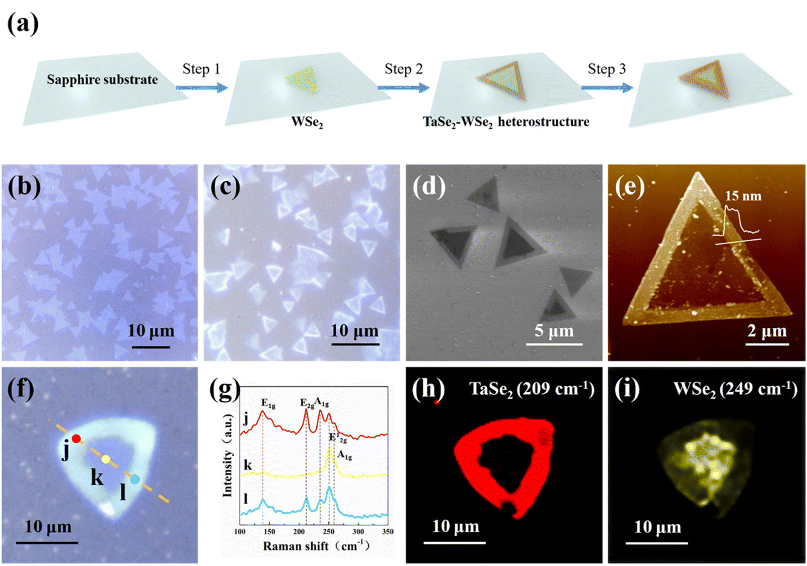 | ||
| Fig. 1 (a) Fabrication strategy for 2D TaSe2-WSe2 heterostructures on the sapphire substrate. Optical images of (b) the large-area monolayer WSe2 and (c) the large-area 2D TaSe2-WSe2 heterostructure. (d) SEM image of 2D TaSe2-WSe2 heterostructures with triangular shapes. (e) AFM image and height profiles of the 2D TaSe2-WSe2 heterostructure. (f) Optical image of a representative 2D TaSe2-WSe2 heterojunction. (g) Raman spectra collected from the regions marked j–l in (f), respectively. (h) and (i) Raman intensity maps of Raman modes at 209 cm−1 (TaSe2) and 249 cm−1 (WSe2), respectively. | ||
Raman spectroscopy was further conducted to study the spatial modulation of the structural and optical characteristics of the 2D TaSe2-WSe2 heterostructures using a 532 nm laser. As shown in Fig. 1f, a typical optical image of a triangular sample used for Raman characterization is displayed. Raman spectra were collected from different areas of the sample to observe the spatial modulation of the heterostructure. As illustrated in Fig. 1g, the Raman spectra obtained from the central region (k in Fig. 1f) exhibit two characteristic peaks at 249 cm−1 and 259 cm−1, corresponding to the E12g, and A1g Raman modes of 2H-WSe2,43 respectively. On the other hand, the Raman spectra collected from the edge area (j and l in Fig. 1f) display five characteristic Raman peaks located at 138 cm−1, 209 cm−1, 234 cm−1, 249 cm−1, and 259 cm−1. Among these, the peaks at 138 cm−1, 209 cm−1, and 234 cm−1 are attributed to the E1g, E2g, and A1g Raman modes of 1T-TaSe2,44 respectively, while the remaining two peaks are related to the Raman modes of 2H-WSe2. Interestingly, the Raman spectra acquired from the edge area exhibited Raman peaks of both TaSe2 and WSe2, indicating the coexistence of the two different materials. To visualize the spatial distribution of TaSe2 and WSe2 in the heterostructure, Raman intensity maps of 209 cm−1 (E2g mode for TaSe2) and 249 cm−1 (E12g mode for WSe2) are generated and shown in Fig. 1h and i, respectively. The Raman intensity map of TaSe2 (Fig. 1h) reveals that the edge area is composed of TaSe2. In the Raman intensity maps of WSe2 (Fig. 1i), the brighter contrast of the central region compared to the edge area is attributed to the fact that most of the Raman signal is shielded by the upper layer of TaSe2. In general, our findings demonstrate the spatial modulation of the structural and optical characteristics of the 2D TaSe2-WSe2 heterostructures.
The elemental composition and crystal structure of the 2D TaSe2-WSe2 heterojunction were first characterized by aberration-corrected scanning transmission electron microscopy (STEM) and energy dispersive X-ray spectroscopy (EDS). A low-magnification high-angle annular dark-field aberration-corrected scanning transmission electron microscopy (HAADF-STEM) image (Fig. 2a) of the 2D TaSe2-WSe2 heterojunction displays a triangular morphology with distinct contrast between the marginal and central regions, indicating a significant difference in thickness between the stacked TaSe2 and the underlying WSe2 layers. EDS maps (Fig. 2b–d) of the red dashed area shown in Fig. 2a reveal that the W element has a uniform intensity distribution, while Ta is present only in the edge area. These findings suggest that the edge portion of the flake sample consists of stacked TaSe2 and the bottom layer is WSe2. Additionally, this analysis is confirmed by selected area electron diffraction (SAED) patterns (Fig. 2e–g) of three different regions (shown in Fig. 2a) labeled with purple (e), yellow (f), and white (g) dots. It is observed that Fig. 2f reveals only one set of six-fold symmetrical diffraction spots, which matched with that of hexagonal WSe2. Due to the lattice constant of 1T-TaSe2 (a = ∼0.345 nm) being slightly larger (mismatch only ∼4.6%) than that of 2H-WSe2 (a = ∼0.329 nm), it is difficult to differentiate the SAED patterns (Fig. 2e and g) of the stacked regions (dots e and g) from those of low-order reflections. However, in the high-order reflections, the spots separate, which allows a chance for identification, as illustrated in Fig. 2h. The enlarged SAED pattern displays two sets of well-aligned six-fold diffraction spots. The inner set (red dotted line) originates from the TaSe2, while the outer set (yellow dotted line) belongs to WSe2. The good alignment of the two sets of spots offers clear and convincing evidence that TaSe2 is grown epitaxially on the underlying WSe2 layer, and the epitaxial relationship between them can be described by (20−20)TaSe2//(20−20)WSe2 and [0001]TaSe2//[0001]WSe2.
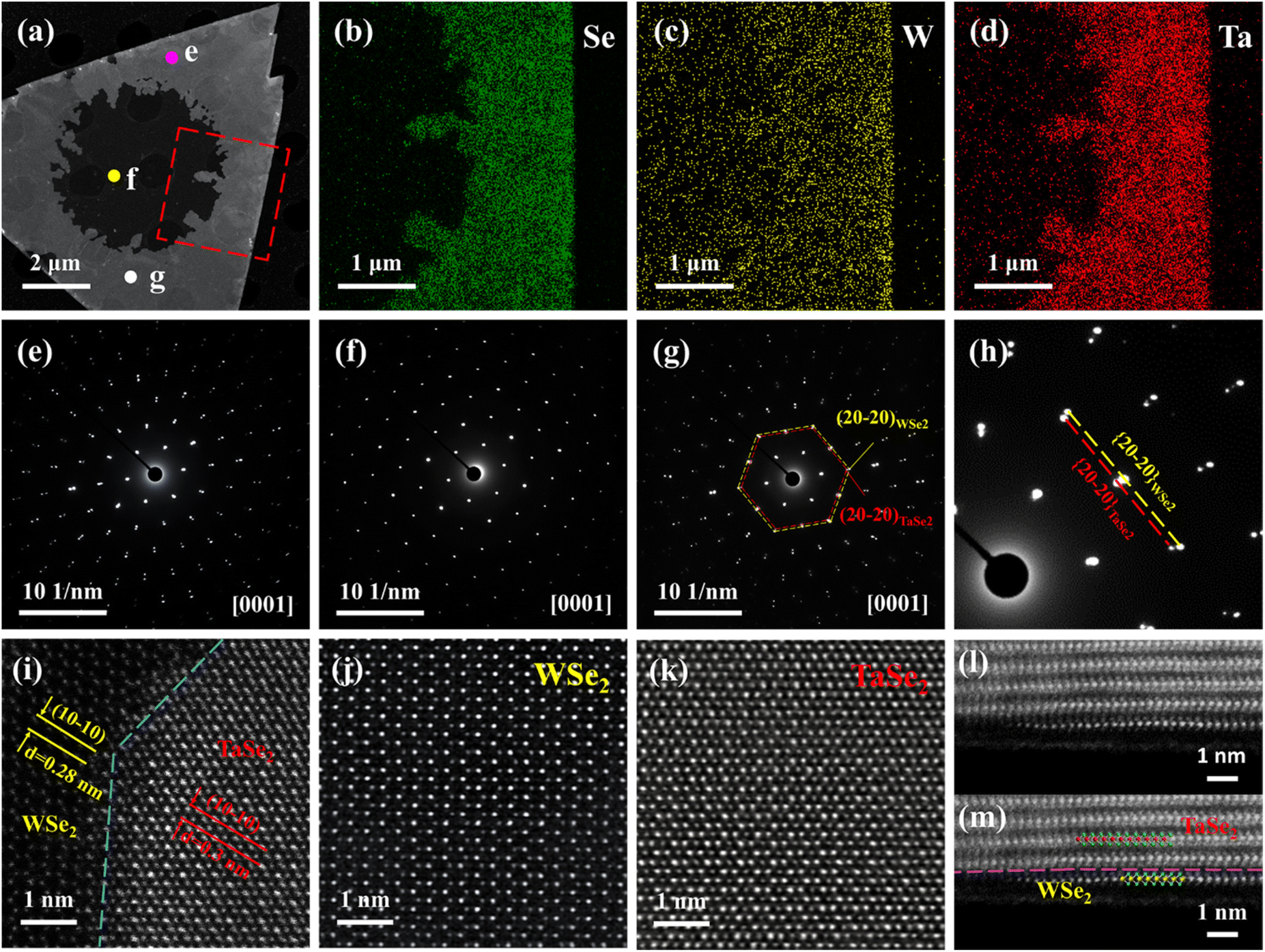 | ||
| Fig. 2 (a) Low-magnification HAADF-STEM image of the 2D TaSe2-WSe2 heterostructure. The stacked regions are labeled with purple dot e and white dot g, and the underlying single-layer WSe2 is labeled with a yellow dot f. (b–d) EDS elemental maps of the 2D heterostructure (red dashed area) for Se, W, and Ta, respectively. (e–g) SAED patterns from the labeled regions (dots e–g) in (a), respectively. (h) Partially enlarged view of the SAED pattern in (g). (i) High-magnification HAADF-STEM image of the interface between the underlying WSe2 and the stacked TaSe2. (j) and (k) Atomic-resolution HAADF-STEM images of WSe2 and TaSe2. (l) and (m) Atomic-resolution cross-sectional HAADF-STEM images with the corresponding atomic model for multilayer 1T-TaSe2 (upper layer) and monolayer 2H-WSe2 (bottom layer). | ||
To further determine the stacking structure of TaSe2 and WSe2, a high-magnification HAADF-STEM image of the 2D TaSe2-WSe2 heterostructure interface was collected and is shown in Fig. 2i. Careful inspection of the interface reveals a clear layer-by-layer stacking interface and well-aligned orientation, thus indicating the vdWs epitaxial growth feature in the vertical stacks. The lattice fringes of the (10−10) plane of TaSe2 and WSe2 are found to be approximately 0.3 nm and 0.28 nm, respectively, which are consistent with the interplanar spacings of 1T-TaSe2 and 2H-WSe2. Furthermore, atomic-resolution HAADF-STEM images of different regions show clear 2H-phase WSe2 and 1T-phase TaSe2 structures, demonstrating the high crystal quality of the heterostructure (Fig. 2j and k). These findings indicate that the two-step CVD method used has not destroyed the underlying WSe2 or produced an alloying phase. Typically, cross-sectional HAADF-STEM images (Fig. 2l and m) show that the upper 1T-TaSe2 is coherently stacked on monolayer 2H-WSe2 across the vdWs gap without any atomic intermixing or damage. Additionally, HAADF-STEM analysis of cross-sectional samples of a 2D multilayer TaSe2 and multilayer WSe2 heterostructure (Fig. S7†) shows that the metal–semiconductor contact interface obtained by chemical vapor phase epitaxial growth is very clean and free of defects. Together, all of these TEM studies prove the successful epitaxy of 1T-TaSe2 on 2H-WSe2 without interlayer rotation misfit. According to published references,45–47 this commensurate TMD heterostructure is expected to reduce the contact resistance compared with that of the randomly twisted stacks, thus showing great application potential in high-performance electronic devices.
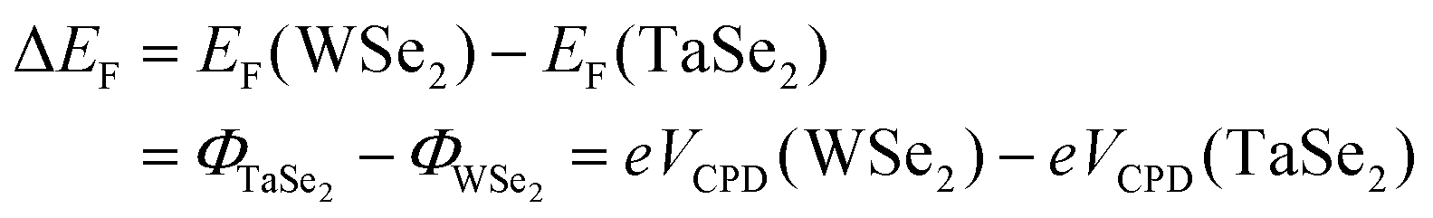
To clarify the underlying mechanism for the exceptional performance of the device based on the 2D TaSe2-WSe2 heterostructure, the interfacial energy level alignment was analyzed using a Kelvin probe force microscope (KPFM). The synthesized 2D metal–semiconductor heterostructures were initially transferred to a Si substrate using a PMMA-assisted transfer method. An AFM morphology image of the 2D TaSe2-WSe2 heterostructure on the Si substrate is presented in Fig. 3a, revealing that multilayer metallic TaSe2 is coherently stacked on the edge of the monolayer WSe2 with an edge height of ∼19 nm. The local surface potential was determined by detecting the interaction between the conductive AFM probe and the sample. As depicted in Fig. 3b, the multilayer TaSe2 displays weaker contrast than the inner monolayer WSe2, while both exhibit stronger contrast with the Si substrate. The local surface potential (VCPD) is specifically calculated using the following equation:
| eVCPD = Φtip − Φsample | (1) |
 | (2) |
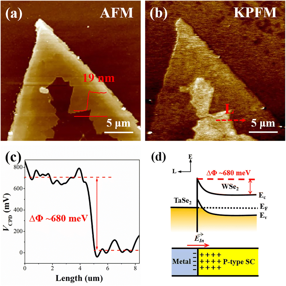 | ||
| Fig. 3 (a) AFM topography image and height profile of a representative 2D TaSe2-WSe2 heterostructure. (b) KPFM surface potential maps of a transferred 2D TaSe2-WSe2 heterostructure on a conductive Si substrate. (c) Contact potential difference along the red dashed line in (b). (d) Corresponding schematics of the band profiles for the 2D TaSe2-WSe2 heterostructure according to KPFM characterization. | ||
Given its distinctive metallic properties, 2D TaSe2 is an excellent electrode material for the fabrication of electronic and optoelectronic devices based on 2D materials (Fig. S8†).51 As shown in Fig. 2l and Fig. S7,† TEM analysis of a cross-sectional sample of 2D TaSe2-WSe2 reveals that the upper multilayer TaSe2 is coherently stacked on a monolayer and multilayer of WSe2 across the vdWs gap without any atomic intermixing or damage. Consequently, compared to traditional thermal evaporation methods, the two-step CVD approach facilitates the epitaxial growth of electrodes, which effectively circumvents damage to the monolayer WSe2 by high-energy metal atoms, thereby reducing surface defects and the Fermi-level pinning effect and enhancing contact performance. Furthermore, to study the epitaxial vdWs contact properties of the TaSe2–WSe2 heterostructure, a series of back-gated FETs were fabricated. Fig. S9† schematically illustrates the process of device preparation. Initially, the heterojunction acquired by two-step CVD growth on sapphire was transferred to (n++) 300 nm-SiO2/Si substrates by the PMMA method. Subsequently, the heterostructures were etched in a helium ion microscope (HIM) using a focused helium ion beam to obtain TaSe2–WSe2 heterostructure ribbons. Finally, 5 nm of Cr and 50 nm of Au were deposited as electrodes by standard electron-beam lithography and thermal evaporation. Further details can be found in the Experimental section. The FETs used the TaSe2–WSe2 heterostructure with WSe2 as the channel semiconductor and TaSe2 nanosheets as the source and drain electrode contacts (Cr/Au metal electrodes were deposited on metallic TaSe2 nanosheets). Fig. 4a and the inset of Fig. 4b depict the schematic model and OM of the FET device based on the TaSe2–WSe2 heterostructure, whereas Fig. 4d and the inset of Fig. 4e show a similar Cr/Au-contacted device constructed on WSe2 for comparison. The Ids–Vds output curve with vdWs TaSe2 contacts (Fig. 4b) is much more linear than that with deposited Cr/Au contacts (Fig. 4e), indicating significantly smaller Schottky barriers in the FET device based on the TaSe2–WSe2 heterostructure. Fig. 4c and f display p-type transfer characteristic curves (Ids–Vg) for TaSe2–WSe2 and WSe2 FET devices. The on-state currents of the TaSe2-contacted and Cr/Au-contacted WSe2 devices are 19 and 5.3 μA at Vd = 0.6 V. Meanwhile, the TaSe2-contacted FET device has an extraordinary on/off ratio exceeding 105 at Vd = 0.2 V, which is much larger than that of the Cr/Au-WSe2 FET device (on/off ratio 103). The field-effect mobilities for the TaSe2-contacted and Cr/Au-contacted WSe2 FETs are estimated to be 23.5 and 8.7 cm2 V−1 s−1 at Vd = 0.2 V, respectively. The on-state current and mobility of the obtained TaSe2-contacted WSe2 FETs are much higher than those of the Cr/Au-contacted WSe2 FETs, which indicate that TaSe2 as an in situ-grown metal electrode on WSe2 can provide superior electrical properties. In addition, we have prepared WSe2 FET devices with TaSe2 and Cr/Au contacts on the same heterostructure and obtained similar experimental results with higher performance for TaSe2 contacts (Fig. S10†). It is essential to obtain the Schottky barrier height (ΦSB) to better understand the charge transport feature in the WSe2 device. Experiments with temperature variations were performed to further explore the ΦSB value of the device. The ΦSB value is then extracted under flat-band conditions. According to Fig. S11e and f,†ΦSB values are around 151 meV (Cr/Au-contacted FET) and 52 meV (TaSe2-contacted FET), respectively. This shows that epitaxial growth of TaSe2 can effectively reduce the Schottky barrier for WSe2 devices. These results demonstrate that the epitaxial growth of 2D TaSe2-WSe2 by a two-step CVD method greatly improves the contact between metal and 2D semiconductors. This work is an important step forward in expanding the range of novel heterostructure materials that can provide more potential applications for high-performance electronic devices.
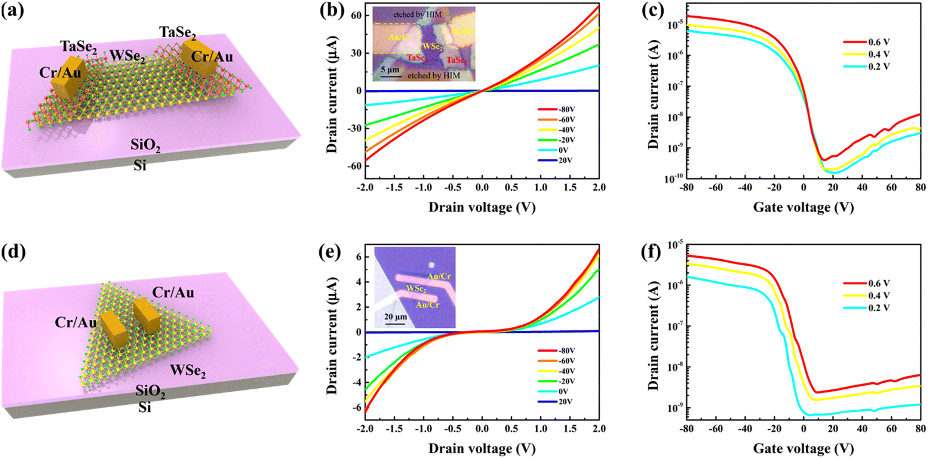 | ||
| Fig. 4 (a) 3D schematic model of the FET device based on the 2D TaSe2-WSe2 heterostructure. (b) Characteristic Ids–Vds output curves of the 2D TaSe2-WSe2 heterostructure at different back-gate voltages. Inset shows an optical image of the 2D TaSe2-WSe2 FET device. (c) Characteristic transfer curves (Ids − Vg) of the 2D TaSe2-WSe2 heterostructure. (d) 3D schematic model of the FET device based on the as-grown WSe2 on the 300 nm-SiO2/Si substrate. (e) Ids–Vds output curves of the WSe2 device collected at room temperature. Inset shows an optical image of a two-electrode WSe2 device. (f) Characteristic transfer curves of the WSe2 device. | ||
Conclusions
In summary, 2D layered TaSe2-WSe2 metal–semiconductor heterostructures have been synthesized on sapphire substrates by depositing TaSe2 on pre-synthesized 2H-WSe2 monolayers using a simple two-step CVD method. TEM studies reveal a clean interface and vdWs epitaxial relationship for (20−20)TaSe2//(20−20)WSe2 and [0001]TaSe2//[0001]WSe2 in 2D TaSe2-WSe2 heterostructures. Furthermore, the analysis of surface potential and electrical transport measurements of this 2D heterostructure reveals that the heterojunction has higher field-effect mobility and on/off ratio. The enhancement of the electronic behavior by the epitaxial growth of metallic vdWs-layered materials can expand the range of metal–semiconductor vertical heterostructure materials and improve the performance of 2D electronic devices.Conflicts of interest
There are no conflicts to declare.Acknowledgements
We are grateful for financial support from the National Key Research and Development Program of China (No. 2021YFF0704705), the Major Research Plan of the National Natural Science Foundation of China (No. 92263205), the Scientific Equipment Development Project of the Chinese Academy of Sciences, and the Youth Innovation Promotion Association Project of the Chinese Academy of Sciences (2020026).References
- G. E. Moore, Proc. IEEE, 1998, 86, 82–85 Search PubMed.
- M. Lundstrom, Science, 2003, 299, 210–211 CrossRef CAS PubMed.
- X. Zhang, Z. C. Lai, Q. L. Ma and H. Zhang, Chem. Soc. Rev., 2018, 47, 3301–3338 RSC.
- J. P. Shi, M. Hong, Z. P. Zhang, Q. Q. Ji and Y. F. Zhang, Coord. Chem. Rev., 2018, 376, 1–19 CrossRef CAS.
- J. Zhou, J. Lin, X. Huang, Y. Zhou, Y. Chen, J. Xia, H. Wang, Y. Xie, H. Yu, J. Lei, D. Wu, F. Liu, Q. Fu, Q. Zeng, C.-H. Hsu, C. Yang, L. Lu, T. Yu, Z. Shen, H. Lin, B. I. Yakobson, Q. Liu, K. Suenaga, G. Liu and Z. Liu, Nature, 2018, 556, 355–359 CrossRef CAS PubMed.
- M. Chhowalla, H. S. Shin, G. Eda, L. J. Li, K. P. Loh and H. Zhang, Nat. Chem., 2013, 5, 263–275 CrossRef PubMed.
- M. Chhowalla, D. Jena and H. Zhang, Nat. Rev. Mater., 2016, 1, 16052 CrossRef CAS.
- J. Xia, X. Huang, L. Z. Liu, M. Wang, L. Wang, B. Huang, D. D. Zhu, J. J. Li, C. Z. Gu and X. M. Meng, Nanoscale, 2014, 6, 8949–8955 RSC.
- J. Xia, Y. X. Zhao, L. Wang, X. Z. Li, Y. Y. Gu, H. Q. Cheng and X. M. Meng, Nanoscale, 2017, 9, 13786–13793 RSC.
- H. N. Jaiswal, M. Liu, S. Shahi, S. Wei, J. Lee, A. Chakravarty, Y. Guo, R. Wang, J. M. Lee, C. Chang, Y. Fu, R. Dixit, X. Liu, C. Yang, F. Yao and H. Li, Adv. Mater., 2020, 32, 2002716 CrossRef CAS PubMed.
- L. Song, L. Ci, H. Lu, P. B. Sorokin, C. Jin, J. Ni, A. G. Kvashnin, D. G. Kvashnin, J. Lou, B. I. Yakobson and P. M. Ajayan, Nano Lett., 2010, 10, 3209–3215 CrossRef CAS PubMed.
- K. F. Mak, C. Lee, J. Hone, J. Shan and T. F. Heinz, Phys. Rev. Lett., 2010, 105, 136805 CrossRef PubMed.
- J.-G. Song, J. Park, W. Lee, T. Choi, H. Jung, C. W. Lee, S.-H. Hwang, J. M. Myoung, J.-H. Jung, S.-H. Kim, C. Lansalot-Matras and H. Kim, ACS Nano, 2013, 7, 11333–11340 CrossRef CAS PubMed.
- D. Wolverson, S. Crampin, A. S. Kazemi, A. Ilie and S. J. Bending, ACS Nano, 2014, 8, 11154–11164 CrossRef CAS PubMed.
- M. Chhowalla, H. S. Shin, G. Eda, L.-J. Li, K. P. Loh and H. Zhang, Nat. Chem., 2013, 5, 263–275 CrossRef PubMed.
- Y. M. Shi, H. N. Li and L. J. Li, Chem. Soc. Rev., 2015, 44, 2744–2756 RSC.
- P. Wang, Y. Huan, P. Yang, M. Cheng, J. Shi and Y. Zhang, Acc. Mater. Res., 2021, 2, 751–763 CrossRef CAS.
- Z. Zhang, P. Yang, M. Hong, S. Jiang, G. Zhao, J. Shi, Q. Xie and Y. Zhang, Nanotechnology, 2019, 30, 182002 CrossRef CAS PubMed.
- L. Xie, M. Liao, S. Wang, H. Yu, L. Du, J. Tang, J. Zhao, J. Zhang, P. Chen, X. Lu, G. Wang, G. Xie, R. Yang, D. Shi and G. Zhang, Adv. Mater., 2017, 29, 1702522 CrossRef PubMed.
- S. B. Desai, S. R. Madhvapathy, A. B. Sachid, J. P. Llinas, Q. X. Wang, G. H. Ahn, G. Pitner, M. J. Kim, J. Bokor, C. M. Hu, H. S. P. Wong and A. Javey, Science, 2016, 354, 99–102 CrossRef CAS PubMed.
- F. Wu, H. Tian, Y. Shen, Z. Hou, J. Ren, G. Gou, Y. Sun, Y. Yang and T.-L. Ren, Nature, 2022, 603, 259–264 CrossRef CAS PubMed.
- A. Allain, J. Kang, K. Banerjee and A. Kis, Nat. Mater., 2015, 14, 1195–1205 CrossRef CAS PubMed.
- J. Tan, S. Li, B. Liu and H. M. Cheng, Small Struct., 2021, 2, 2000093 CrossRef CAS.
- A. Razavieh, P. Zeitzoff and E. J. Nowak, IEEE Trans. Nanotechnol., 2019, 18, 999–1004 CAS.
- S. G. Louie and M. L. Cohen, Phys. Rev. B: Solid State, 1976, 13, 2461–2469 CrossRef CAS.
- C. Kim, I. Moon, D. Lee, M. S. Choi, F. Ahmed, S. Nam, Y. Cho, H.-J. Shin, S. Park and W. J. Yoo, ACS Nano, 2017, 11, 1588–1596 CrossRef CAS PubMed.
- T. Nishimura, K. Kita and A. Toriumi, Appl. Phys. Lett., 2007, 91, 123123.123121–123123.123123 Search PubMed.
- A. Pirkle, J. Chan, A. Venugopal, D. Hinojos, C. W. Magnuson, S. McDonnell, L. Colombo, E. M. Vogel, R. S. Ruoff and R. M. Wallace, Appl. Phys. Lett., 2011, 99, 122108–122108 CrossRef.
- J. Jang, H.-S. Ra, J. Ahn, T. W. Kim, S. H. Song, S. Park, T. Taniguch, K. Watanabe, K. Lee and D. K. Hwang, Adv. Mater., 2022, 34, 2109899 CrossRef CAS PubMed.
- Z. H. Cheng, Y. F. Yu, S. Singh, K. Price, S. G. Noyce, Y. C. Lin, L. Y. Cao and A. D. Franklin, Nano Lett., 2019, 19, 5077–5085 CrossRef CAS PubMed.
- A. Jain, A. Szabo, M. Parzefall, E. Bonvin, T. Taniguchi, K. Watanabe, P. Bharadwaj, M. Luisier and L. Novotny, Nano Lett., 2019, 19, 6914–6923 CrossRef CAS PubMed.
- R. Kappera, D. Voiry, S. E. Yalcin, B. Branch, G. Gupta, A. D. Mohite and M. Chhowalla, Nat. Mater., 2014, 13, 1128 CrossRef CAS PubMed.
- J. H. Sung, H. Heo, S. Si, Y. H. Kim, H. R. Noh, K. Song, J. Kim, C. S. Lee, S. Y. Seo, D. H. Kim, H. K. Kim, H. W. Yeom, T. H. Kim, S. Y. Choi, J. S. Kim and M. H. Jo, Nat. Nanotechnol., 2017, 12, 1064–1070 CrossRef CAS PubMed.
- X. Cui, G. H. Lee, Y. D. Kim, G. Arefe, P. Y. Huang, C. H. Lee, D. A. Chenet, X. Zhang, L. Wang, F. Ye, F. Pizzocchero, B. S. Jessen, K. Watanabe, T. Taniguchi, D. A. Muller, T. Low, P. Kim and J. Hone, Nat. Nanotechnol., 2015, 10, 534–540 CrossRef CAS PubMed.
- Y. Liu, J. Guo, E. Zhu, L. Liao, S.-J. Lee, M. Ding, I. Shakir, V. Gambin, Y. Huang and X. Duan, Nature, 2018, 557, 696–700 CrossRef CAS PubMed.
- X. K. Zhai, X. Xu, J. B. Peng, F. L. Jing, Q. L. Zhang, H. J. Liu and Z. G. Hu, ACS Appl. Mater. Interfaces, 2020, 12, 24093–24101 CrossRef CAS PubMed.
- Z. P. Zhang, Y. Gong, X. L. Zou, P. Liu, P. F. Yang, J. P. Shi, L. Y. Zhao, Q. Zhang, L. Gu and Y. F. Zhang, ACS Nano, 2019, 13, 885–893 CrossRef CAS PubMed.
- Y. Zhang, L. Yin, J. W. Chu, T. A. Shifa, J. Xia, F. Wang, Y. Wen, X. Y. Zhan, Z. X. Wang and J. He, Adv. Mater., 2018, 30, 1803665 CrossRef PubMed.
- Q. D. Fu, X. W. Wang, J. D. Zhou, J. Xia, Q. S. Zeng, D. H. Lv, C. Zhu, X. L. Wang, Y. Shen, X. M. Li, Y. N. Hua, F. C. Liu, Z. X. Shen, C. H. Jin and Z. Liu, Chem. Mater., 2018, 30, 4001–4007 CrossRef CAS.
- C. S. Lee, S. J. Oh, H. Heo, S. Y. Seo, J. Kim, Y. H. Kim, D. Kim, O. F. N. Okello, H. Shin, J. H. Sung, S. Y. Choi, J. S. Kim, J. K. Kim and M. H. Jo, Nano Lett., 2019, 19, 1814–1820 CrossRef CAS PubMed.
- V. T. Vu, T. T. H. Vu, T. L. Phan, W. T. Kang, Y. R. Kim, M. D. Tran, H. T. T. Nguyen, Y. H. Lee and W. J. Yu, ACS Nano, 2021, 15, 13031–13040 CrossRef CAS PubMed.
- P. Y. Qiao, J. Xia, X. Z. Li, F. Ru, P. Liu, L. F. Tian, X. X. Jiang, Z. S. Lin, X. Chen and X. M. Meng, Adv. Funct. Mater., 2022, 32, 2201449 CrossRef CAS.
- B. L. Liu, M. Fathi, L. Chen, A. Abbas, Y. Q. Ma and C. W. Zhou, ACS Nano, 2015, 9, 6119–6127 CrossRef CAS PubMed.
- J. C. Tsang, J. E. Smith, M. W. Shafer and S. F. Meyer, Phys. Rev. B: Solid State, 1977, 16, 4239–4245 CrossRef CAS.
- J. Zhang, J. H. Wang, P. Chen, Y. Sun, S. Wu, Z. Y. Jia, X. B. Lu, H. Yu, W. Chen, J. Q. Zhu, G. B. Xie, R. Yang, D. X. Shi, X. L. Xu, J. Y. Xiang, K. H. Liu and G. Y. Zhang, Adv. Mater., 2016, 28, 1950–1956 CrossRef CAS PubMed.
- M. Liao, Z.-W. Wu, L. Du, T. Zhang, Z. Wei, J. Zhu, H. Yu, J. Tang, L. Gu, Y. Xing, R. Yang, D. Shi, Y. Yao and G. Zhang, Nat. Commun., 2018, 9, 4068 CrossRef PubMed.
- K. Liu, L. Zhang, T. Cao, C. Jin, D. Qiu, Q. Zhou, A. Zettl, P. Yang, S. G. Louie and F. Wang, Nat. Commun., 2014, 5, 4966 CrossRef CAS PubMed.
- Y. Gao, Y. L. Hong, L. C. Yin, Z. T. Wu, Z. Q. Yang, M. L. Chen, Z. B. Liu, T. Ma, D. M. Sun, Z. H. Ni, X. L. Ma, H. M. Cheng and W. C. Ren, Adv. Mater., 2017, 29, 1700990 CrossRef PubMed.
- Q. Cheng, J. Pang, D. Sun, J. Wang, S. Zhang, F. Liu, Y. Chen, R. Yang, N. Liang, X. Lu, Y. Ji, J. Wang, C. Zhang, Y. Sang, H. Liu and W. Zhou, InfoMat, 2020, 2, 656–697 CrossRef CAS.
- S. M. Sze and K. K. Ng, Physics of semiconductor devices, Wiley-Interscience, Hoboken, N.J., 3rd edn, 2007 Search PubMed.
- J. Shi, X. Chen, L. Zhao, Y. Gong, M. Hong, Y. Huan, Z. Zhang, P. Yang, Y. Li, Q. Zhang, Q. Zhang, L. Gu, H. Chen, J. Wang, S. Deng, N. Xu and Y. Zhang, Adv. Mater., 2018, 30, 1804616 CrossRef PubMed.
Footnote |
| † Electronic supplementary information (ESI) available: Further details of the experimental design. OM, SEM, Raman, and AFM characterization of WSe2 and TaSe2. HAADF-STEM analysis of cross-sectional samples of 2D multilayer TaSe2 and multilayer WSe2 heterostructures. Schematic diagram of FET device preparation. See DOI: https://doi.org/10.1039/d3nr03538g |
| This journal is © The Royal Society of Chemistry 2023 |