
Lateral surface passivation of CdSe nanoplatelets through crown management†
Huan
Liu
ab,
Peixian
Chen
c,
Xuanyu
Zhang
b,
Xiongbin
Wang
b,
Tingchao
He
 *c and
Rui
Chen
*b
*c and
Rui
Chen
*b
aHarbin Institute of Technology, Harbin 150001, China
bDepartment of Electrical and Electronic Engineering, Southern University of Science and Technology, Shenzhen 518055, China. E-mail: chenr@sustech.edu.cn
cKey Laboratory of Optoelectronic Devices and Systems of Ministry of Education and Guangdong Province, College of Physics and Optoelectronic Engineering, Shenzhen University, Shenzhen 518060, China. E-mail: tche@szu.edu.cn
First published on 10th August 2023
Abstract
Two-dimensional colloidal CdSe nanoplatelets (NPLs) have been considered as ideal emitting materials for high performance light-emitting devices due to their excellent optical properties. However, the understanding of defect related radiative and nonradiative recombination centers in CdSe NPLs is still far from sufficient, especially their physical distribution locations. In this work, CdSe core and CdSe/CdS core/crown NPLs have been successfully synthesized and their optical properties have been characterized by laser spectroscopies. It is found that the photoluminescence quantum yield of CdSe NPLs is improved by a factor of 4 after the growth of the CdS crown. At low temperatures, the change in the ratio of low and high energy emission intensities from NPLs suggests that the radiative recombination centers are mainly located on the lateral surface of the samples. This finding is further confirmed by the surface passivation experiment. Meanwhile, the nonradiative recombination centers of NPLs located on the lateral surface are also confirmed by ligand exchange. These results demonstrate the importance of understanding the optical properties of the lateral surface of NPLs, which are important for the design of material structures for optoelectronic applications.
Introduction
Low-dimensional colloidal semiconductor nanocrystals have attracted considerable research interest over the past 30 years due to their unique optical properties resulting from the strong quantum confinement and surface effect.1 The controlled synthesis of nanocrystals offers the possibility to manipulate their optical properties by changing their composition, size, structure, and morphology.2–4 In 2006, the CdSe nanoplatelets (NPLs) with a thickness of a few atomic layers were synthesized for the first time by Hyeon et al.5 The NPLs exhibit well-defined fluorescence with narrow linewidth due to the precise control of the material thickness. Compared with various structures such as zero-dimensional quantum dots (QDs) and one-dimensional nanorods, NPLs possess fascinating optical properties such as narrow band emission, large absorption cross-section, strong oscillator strength, and long Auger recombination lifetime.6–12 These outstanding properties have attacted great interest and breakthroughs from researchers in the field of light-emitting diodes with wide color gamut and optically pumped lasers with low threshold.13,14Due to the large surface-to-volume ratio, the highest PLQY of bare-core CdSe NPLs does not exceed 50%. One solution to overcome this problem is surface ligand exchange, such as replacing the cadmium carboxylates on the surface of CdSe NPLs with halides.15,16 Although this method can improve the performance of NPLs in solution, these materials exhibit weak emission in thin film, which hinders their potential in device applications. Another approach is heteroepitaxy, which has been shown to work with QDs. According to the special layer structure, the NPLs heterostructures can be divided into vertical (core/shell) and lateral (core/crown) structures, both of which can enhance the optical performance of NPLs to a certain extent.17 However, until now, the understanding of defect realted radiative and nonradiative recombination centers in CdSe NPLs is far from adequate, especially their physical distribution locations. In particular, the physical mechanism of the two close emissions from CdSe NPLs at low temperatures is still controversial.16,18–20 Some efforts have been made to explain the origin of the low-energy peak. For example, it may originate from phonon-line emission due to the self-stacking of CdSe NPLs.20 Norris et al. proposed that the low energy peak of CdSe NPLs may originate from trion emission.19 Our recent result suggested that the low energy peak is closely related to the surface state of the NPLs, which was confirmed by size-dependent and surface passivation experiments.18 Besides, it is generally believed that the radiative and nonradiative recombination centers are mainly located on the top and bottom surfaces of NPLs. However, some studies have pointed out that the surface in the lateral direction has a stronger influence.17,21,22 Therefore, a more detailed discussion and analysis of the radiative and nonradiative recombination centers in CdSe NPLs is urgently needed for structural design and their future applications.
In this work, CdSe/CdS core/crown (C/C) NPLs have been synthesized based on CdSe core (C) NPLs. The optical properties of two NPLs are systematically investigated to discuss the distribution locations of defect realted radiative and nonradiative recombination in NPLs. Lateral surface passivation not only enhances the photoluminescence quantum yield (PLQY) of C NPLs, but also suppresses the low energy emission at low temperatures. Interestingly, the surface trap states associated with low energy emission of C NPLs can be effectively suppressed by polydimethylsiloxane (PDMS), but the suppression effect on the C/C NPLs is not obvious. The results show that the radiative recombination centers are mainly located on the lateral surface of the NPLs rather than the vertical surface. Moreover, the PLQY of C NPLs was enhanced 8-fold after ligand exchange, while weak changes were found in the PLQY of C/C NPLs, which confirms that the nonradiative recombination centers of NPLs are also located on the lateral surface.
Results and discussion
The synthesis and characterization methods for C and C/C NPLs are presented in the Experimental section. The scanning transmission electron microscopy (STEM) images of two samples are shown in Fig. 1a and b, where the insets are their schematic structures. The average lengths and widths of C and C/C NPLs were approximately 42.0 (±2.2) × 8.8 (±0.2), and 42.7 (±1.2) × 10.2 (±0.2) nm, respectively. Compared to C NPLs, the larger size of C/C NPLs indicates the successful lateral growth of CdS crowns. The 0.7 nm CdS crown is a very small value in the longer lateral direction probably in the measurement error. Note that the white lines in the STEM images are curled NPLs due to the interaction between the NPLs, which are not included in the statistics. The normalized absorption and PL spectra of C and C/C NPLs are shown in Fig. 1c. Similar to most of the 4.5 monolayer thick C NPLs,20,23,24 two sharp absorption peaks at 482 and 512 nm can be clearly observed, which correspond to the light and heavy hole transitions, respectively. For the C/C NPLs, the weak absorption located at 400 nm is related to the thin CdS crown.23 The C and C/C NPLs have the same emission peak at 513 nm, indicating that they have the same recombination channel. According to the small conduction band offset and large valence band offset between CdSe and CdS, the type I band alignment can be determined for C/C NPLs.25 Due to the thin CdS crown, the C/C NPLs exhibit similar emission with C NPLs. The PLQY increases more than 4 times from 6.5% for C NPLs to 28.0% for C/C NPLs, which can be attributed to the effective passivation of nonradiative recombination centers by the CdS crown. As shown in Fig. 1d, the time-resolved photoluminescence (TRPL) of C and C/C NPLs probed at 513 nm can be fitted with a triexponential function, and the average decay lifetimes were calculated to be 2.95 and 2.94 ns respectively. Their decay channels and their percentages are summarized in Table S1 (ESI†). In general, the fast decay component in CdSe nanocrystals can be considered as the nonradiative decay channel due to the poor surface passivation and cadmium vacancies.26 Compared with C NPLs, the nonradiative decay rate of C/C NPLs is two times smaller than that of C NPLs. This result indicates that the nonradiative recombination centers (hole trapping) on the lateral surfaces are effectively passivated by the CdS crown. Besides, the C NPLs delayed emission is attributed to the hole trapping–detrapping process that slows down the exciton recombination without causing additional emission band.21,27 | ||
| Fig. 1 STEM image of (a) C, (b) C/C NPLs. Insets are the schematic diagrams of their corresponding structures. (c) Normalized UV-visible absorption and PL spectra of C and C/C NPLs. Inset is the image of samples under UV light illumination. (d) Room temperature TRPL of C and C/C NPLs. | ||
To gain a deeper understanding of the radiative recombination centers of C NPLs, the measurements of PL spectra of C and C/C NPLs were performed from 50 to 300 K (data shown in Fig. 2a and S1,† respectively). In order to avoid the influence of stacking on the NPLs emission, C and C/C NPLs solution with absorbance of 0.2 at 512 nm is spun-coated on a quartz substrate.19 Apparently, only one PL peak can be observed at 300 K (513 nm). However, as the temperature decreases, another sharp peak appears on the low energy side at 220 K and reaches its maximum at 50 K. The pre-existing emission peak labeled as P1 comes from free exciton recombination,18,19 while the origin of the low energy peak (P2) will be discussed later. The two-color emission of C/C NPLs behave like C NPLs, indicating that indeed part of the C lateral surface remains unpassivated. The P1 and P2 of C and C/C NPLs show a similar redshift with increasing temperature from 50 to 220 K, and the energy difference between the two peaks remains constant at around 29 meV (Fig. 2b). The result is consistent with our previous measurements of C NPLs with different lateral sizes.18 Although the energy difference between the two emissions is close to the longitudinal phonon energy (25 meV) of bulk CdSe material, this value is too small to support the exciton transition for P2. The full width at half maximum (FWHM) of P1 and P2 for C and C/C NPLs were obtained by Lorentz fitting and are shown in Fig. 2c and d, respectively. Notably, larger FWHM values can be observed for P1 of C and C/C NPLs with the increase of temperature, which is due to the electron–phonon coupling.28 Therefore, the identical FWHM of the P2 at different temperatures can be attributed to the weak interaction between electrons and phonons. Based on the discussion above, P2 resulting from phonon replica can be further excluded.
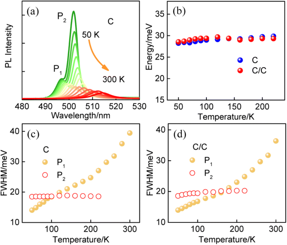 | ||
| Fig. 2 (a) Temperature-dependent PL spectra of C NPLs. (b) Energy difference of P1 and P2 of C and C/C NPLs. (c) FWHM of the P1 and P2 of C NPLs at different temperatures. (d) FWHM of the P1 and P2 of C/C NPLs at different temperatures. | ||
To further discuss the characteristics of P2, power-dependent PL spectra from C and C/C NPLs were measured at 50 K and shown in Fig. 3a and b. To facilitate comparison, all the curves are normalized to P2. The two emissions show different trends with excitation power from 0.05 to 20 mW. Relative to C, a weaker redshift is found in C/C NPLs due to the passivation of the lateral nonradiative recombination centers. At the same time, it can be found that the PL intensity of P1 relative to P2 decreases with increasing excitation power for the NPLs. For visual comparison, the corresponding PL intensity ratios of P2 to P1 are plotted in Fig. 3c and d. Under the lowest excitation power, the PL intensity ratios of P2 to P1 for C and C/C NPLs are 3.8 and 2.4, respectively. Furthermore, it can be seen that the ratios for C and C/C NPLs saturate at 20 and 13 mW, respectively, with the increase of excitation power. The faster saturation and smaller ratio in C/C NPLs can be attributed to the passivation of lateral surface trap states by CdS crowns.18 Due to the presence of additional surface trap states in the C NPLs, higher power is required to achieve the saturation of P2. To confirm this guess, C/C NPLs with thicker crown (named C/C-10 and C/C-20) were synthesized. Their absorption, PL (Fig. S2†) and PLQY were characterized. It was found that C/C NPLs exhibited higher PLQY with increasing CdS thickness. Furthermore, compared with C and C/C NPLs, the P2 of C/C-10 and C/C-20 NPLs is further suppressed (Fig. S3†). Therefore, it is verified that the P2 intensity is related to the surface trap states. In addition, the temperature-dependent PL spectra of C NPLs were measured from 80 to 300 K under Xenon lamp excitation (Fig. S4†). Unlike the laser excitation at 0.05 mW, the C NPLs under Xenon lamp excitation show only P2 at 80 and 100 K, and the intensity of P2 is much weaker than that of P1. The result again indicates that P2 associated with the surface trap state is closely related to the excitation power.
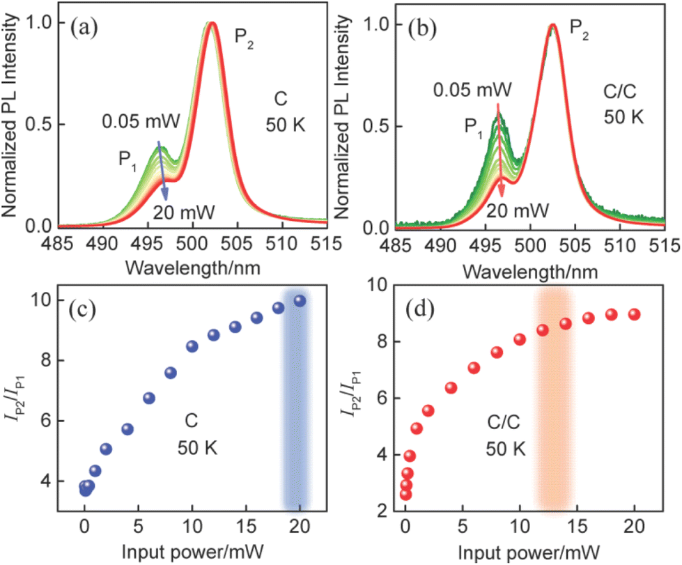 | ||
| Fig. 3 Power-dependent PL spectra of (a) C and (b) C/C NPLs at 50 K. (c) C and (d) C/C NPLs Power-dependent ratio of P2/P1. The cylinders represent the initial saturation power of C and C/C NPLs, respectively. | ||
Although our previous work has confirmed that PDMS can effectively suppress the P2 of C NPLs, it is unclear whether the P2 is related to the lateral or vertical surface of NPLs.16 To clarify the location of the surface trap states associated with P2 in NPLs, PDMS was used to passivate the two NPLs. The temperature-dependent PL spectra of C and C/C NPLs were measured under identical experimental conditions. Their PL spectra at 50 K are shown in Fig. 4a and b. Interestingly, the P2 intensities for C NPLs are significantly reduced after PDMS encapsulation.18 However, only a slight change can be observed for the C/C NPLs. It is obvious that PDMS encapsulation passivates not only the vertical surface but also the lateral surface of C NPLs. However, only the vertical surfaces were passivated by PDMS for C/C NPLs, since the lateral surfaces of C/C were protected by CdS crowns. The results here show that the surface trap states associated with P2 (radiative recombination center) are more strongly correlated with the lateral surface trap states of the C NPLs, rather than the vertical surface which has a larger surface area.
 | ||
| Fig. 4 Normalized PL spectra of the samples before and after PDMS treatment (a) C and (b) C/C NPLs at 50 K. Inset: images of the samples before and after PDMS treatment under UV light illumination. | ||
As mentioned above, the CdS crown not only passivates the surface trap states associated with P2, but also enhances the PLQY of C NPLs. To further verify the importance of lateral surface passivation on the optical performance of C NPLs, ligand exchange experiments were carried out and the optical properties of C and C/C NPLs were characterized. For simplicity, C and C/C NPLs after ligand exchange are referred as C–Br and C/C–Br NPLs, respectively. The PL images during ligand exchange at different times for C–Br and C/C–Br NPLs are shown in Fig. S5a–e.† The emission from the C–Br and C/C–Br NPLs was completely quenched after OLA and cadmium bromide were added to the primary solution. Interestingly, after 0.5 h, the weak emission was only observed in C–Br but not in C/C–Br NPLs. Furthermore, it is noteworthy that C–Br NPLs is brighter than C/C–Br NPLs under UV lamp illumination after ligand exchange (Fig. S5a vs. e†). It is obvious that ligand exchange not only passivates the vertical surface but also the lateral surface of C NPLs. However, for C/C NPL, the lateral surface of CdSe core does not undergo ligand exchange because the it is protected by the CdS crown. The result is consistent with the PDMS passivation shown above.
To better understand the effect of ligand exchange on the optical properties of the materials, PL, TRPL and PLQY of C–Br and C/C–Br NPLs were also recorded. The normalized absorption and PL spectra of C–Br and C/C–Br NPLs are shown in Fig. 5a. With respect to the as-grown NPLs, the emissions of C–Br and C/C–Br NPLs shift from 513 to 528 nm, and the FWHM increases from 8 to 13 nm.15,16,29 The redshift and broadening of the PL spectra may be related to the lattice expansion in the vertical direction.24,30 The STEM images of C–Br and C/C–Br NPLs after ligand exchange are shown in Fig. S6.† The unchanged morphology suggests that the difference in optical properties is due to the ligand exchange. Compared to the original NPLs, the PLQY of C–Br was enhanced 8-fold after ligand exchange, while C/C–Br NPLs only showed only a slight change (Fig. 5b). The small increase in PLQY of C/C NPLs can be attributed to the incomplete passivation of lateral surface. In addition, the TRPL and decay channel of the treated NPLs monitored at 528 nm are shown in Fig. S7 and Table S1,† respectively. Compared to the TRPL before ligand exchange, the decay channel associated with C–Br nonradiative recombination was slowed down by a factor of 2.9, while the changes in C/C–Br NPLs were weak. Again, the tremendous change in photophysical properties of C–Br NPLs can be attributed to the passivation of nonradiative recombination centers on the lateral surfaces. In previous experiments,21,22,30 the emission of C NPLs was completely quenched by stripping the ligands of C NPLs on the lateral and vertical surfaces by n-butylamine, but still 40% of the PL intensity was observed in the C/C NPLs due to the presence of CdS crowns.21 Recent studies have shown that the PLQY of C NPLs can be enhanced from 20% to 100% after passivation of lateral surface defects by CdSeS crown.31 In addition, theoretical calculations proved that the binding energy of cadmium carboxylate in the vertical surfaces is larger than that in the lateral surfaces, which leads to the formation of more defects in the lateral plane.21,22 Therefore, based on the above results, it can be assumed that the nonradiative recombination centers of the NPLs are also distributed on the lateral surfaces rather than the larger vertical one.
 | ||
| Fig. 5 (a) Normalized absorption and PL spectra of C and C/C NPLs after 5 h of ligand exchange. (b) PLQYs before and after ligand exchange for C and C/C NPLs. Insets: images of the samples before and after ligand exchange under UV light illumination. | ||
Next, we put forward our speculation on the origin of P2 based on the reported literature and data. Just as discussed above, P2 has been shown to correlate with the lateral surface trap states of the NPLs. In some recent reports, P2 is considered to be negative trion emission.19,32–34 In addition, it was found that the gain threshold can be further reduced and the Auger recombination lifetime can be extended at low temperatures for NPLs.10,19 This indicates that multiexcitons can be easily generated at low temperatures. In parallel, for low-dimensional CdSe, hole trapping is the main primary mechanism of carrier trapping.35,36 For NPLs, it has been shown that the C NPLs are Cd-rich and passivated by carboxylates. However, the binding energy of cadmium carboxylate on the lateral surface (43.8 kJ mol−1) is lower than that on the vertical surface (74.3 kJ mol−1).21 The weak binding energy on the lateral surface results in hole trapping due to Cd vacancies.22 In this scenario, negative trions can be easily formed after the trapping of biexciton in a hole. Besides, the gradual disappearance of P2 as the temperature increases to 220 K indicates that the hole are released assisted by thermal energy, which is consistent with the fluorescence decay process. Therefore, when there are numerous hole traps on the lateral surfaces, more pronounced P2 will be observed. At the same time, P2 of C/C NPLs with better lateral surface passivation is more easily to be saturated. The weak P2 has been observed under Xenon lamp excitation because the number of multi-excitons generated is much smaller than that under laser excitation due to the different excitation power.
Conclusions
In summary, the optical properties of C and C/C NPLs were comparatively investigated. It is found that the optical properties of C NPLs changed significantly after the lateral surface passivation by CdS crown. At the low temperature, the P2 intensities of C/C are suppressed due to the lateral surface passivation. At the same time, P2 intensity in C/C NPLs was more easily saturated with the increase of excitation power compared with C NPLs. The PDMS encapsulation further proves that the surface trap states associated with P2 (radiative recombination center) of C NPLs mainly originate from the lateral surface rather than the vertical surface. In addition, the nonradiative recombination centers of C NPLs located on the lateral surface were also confirmed by ligand exchange experiment. These experimental results demonstrate the importance of lateral surface trap state passivation on the radiative and nonradiative recombination centers of NPLs, which is crucial for either the design or application of NPLs in optoelectronic devices.Experimental section
Chemicals
Cadmium oxide (99.999%), cadmium(II) acetate (Cd(OAc)2; 99.995%), cadmium acetate dihydrate (Cd(OAc)2·2H2O), selenium powder (Se; 99.99%) and sulfur (S; 99.9%) were purchased from Aladdin. Sodium myristate (99%) and cadmium nitrate tetrahydrate (99.997%) were purchased from Sigma-Aldrich. Octadecene (ODE; 90%), oleylamine (OLA, 90%), oleic acid (OA, 90%), trioctylphosphine (TOP; 90%), propionic acid (99.5%), methanol (99.9%) and hexane (95%) were purchased from Macklin.Synthesis of CdSe NPLs
Cadmium myristate (Cd(Myr)2), C and C/C NPLs were synthesized according to the reported methods.23 Typically, 170 mg cadmium myristate, 10 mg selenium powder, and 15 mL ODE were put into a three-necked flask, and then degassed three times at 80 °C. Subsequently, the temperature was set at 240 °C, and when the solution was heated to 195 °C, 40 mg Cd(OAc)2·2H2O was added rapidly, followed by a reaction at 240 °C for 10 min. After the reaction was stopped, 0.5 mL OA was added and subsequently cooled to 25 °C for purification purpose. In the crude solution, alcohol and hexane were added followed by centrifugation at 5000 rpm for 5 min, the supernatant was discarded and the precipitate was dispersed in hexane.Synthesis of CdSe/CdS NPLs
The ODE-S was obtained by sonicating 32 mg S powder and 10 mL ODE for 5 min. The CdS precursor was then obtained by mixing 3 mL ODE, 2 mL ODE-S, 0.35 mL OA and 400 mg Cd(OAc)2·2H2O and then sonicating for 2 hours. The mixture was stirred and held under vacuum at 110 °C for 20 min. The C NPLs were dried under a stream of nitrogen in a 50 mL three-neck flask. Subsequently, 12 mL ODE and 100 mg Cd(propionate)2 were added to the flask. After completing this step, the mixture was heated to 235 °C under a nitrogen stream. Using a syringe pump, CdS precursor solution was injected at a speed of 3 mL h−1 in 5, 10, and 20 min. After reacting at 235 °C for another 5 min, the heating plate was removed and the crude solution was cooled to 25 °C. When the temperature of the mixture cooled to 160 °C, 2 mL OA was added. The crude solution was dispersed into 20 mL hexane and then centrifuged at 6000 rpm for 10 min. The obtained supernatant was discarded and the precipitate was redispersed in hexane.Morphology and optical characterization
The morphologies of C and C/C NPLs were characterized by FEI Talos 200X STEM. Steady-state absorption and PL spectra were obtained using a Lambda 950 UV-Vis spectrophotometer (PerkinElmer, Inc.) and fluorescence spectrometer (Edinburgh Instruments, FS5), respectively. During the PLQY measurement, the NPLs’ solution was filled into the cuvette with 1 cm optical length and placed in an integrated sphere, and then excited by 350 nm light generated by a Xeon lamp. The time-correlated single photon counting technique (Edinburgh Instruments, FS5) was used to collect the TRPL of the samples. Temperature-dependent PL spectra (from 50 to 300 K) of C and C/C NPLs were recorded by a home-built liquid helium closed-cycle system with excitation at 325 nm from a He–Cd laser. The C NPLs under Xenon lamp excitation temperature-dependent PL spectra (from 80 to 300 K) were recorded by fluorescence spectrometer (Edinburgh Instruments, FS5). Prior to measurement, the NPLs solution was drop cast onto a quartz and then placed in a liquid nitrogen cooled cryostat.PDMS passivation and ligand exchange
Liquid silicon matrix and curing agent were mixed at a ratio of 10![[thin space (1/6-em)]](https://www.rsc.org/images/entities/char_2009.gif) :1 to obtain a PDMS solution, which was then drop casted onto a sample loaded quartz plate and dried under vacuum. Ligand exchange of C and C/C NPLs was performed according to the method reported in previous literature.15 A new ligand solution was prepared by sonicating 13.6 mg cadmium bromide with 1 mL methanol for 5 min. During the ligand exchange process, 3 mL toluene was added to 0.3 mL NPLs’ solution (absorbance at 512 nm is 0.21), followed by 20 μL OLA and 30 μL cadmium bromide–methanol solution. The PL of the NPLs was quenched after the addition of OLA, but it reappeared after 0.5–5 hours.
:1 to obtain a PDMS solution, which was then drop casted onto a sample loaded quartz plate and dried under vacuum. Ligand exchange of C and C/C NPLs was performed according to the method reported in previous literature.15 A new ligand solution was prepared by sonicating 13.6 mg cadmium bromide with 1 mL methanol for 5 min. During the ligand exchange process, 3 mL toluene was added to 0.3 mL NPLs’ solution (absorbance at 512 nm is 0.21), followed by 20 μL OLA and 30 μL cadmium bromide–methanol solution. The PL of the NPLs was quenched after the addition of OLA, but it reappeared after 0.5–5 hours.
Author contributions
The manuscript was written through contributions of all authors. All authors have given approval to the final version of the manuscript.Conflicts of interest
There are no conflicts to declare.Acknowledgements
This work is supported by the National Natural Science Foundation of China (62174079), Science, Technology and Innovation Commission of Shenzhen Municipality (Projects No. JCYJ20220530113015035, JCYJ20210324120204011, JCYJ20190808121211510, and KQTD2015071710313656).References
- J. M. Pietryga, Y. S. Park, J. Lim, A. F. Fidler, W. K. Bae, S. Brovelli and V. I. Klimov, Chem. Rev., 2016, 116, 10513–10622 CrossRef CAS PubMed.
- R. X. Li, B. B. Li, X. Fang, D. K. Wang, Y. Q. Shi, X. Liu, R. Chen and Z. P. Wei, Adv. Mater., 2021, 33, 2100466 CrossRef CAS PubMed.
- H. Liu, J. Hao, J. Li, J. Cheng, Y. Gao, X. Lin, K. Wang and T. He, J. Phys. Chem. C, 2020, 124, 27840–27847 CrossRef CAS.
- Y. Wu, Z. Huang, Q. Sun, V. D. Ta, S. Wang and Y. Wang, Laser Photonics Rev., 2023, 17, 2200703 CrossRef CAS.
- J. Joo, J. S. Son, S. G. Kwon, J. H. Yu and T. Hyeon, J. Am. Chem. Soc., 2006, 128, 5632–5633 CrossRef CAS PubMed.
- W. Cho, S. Kim, I. Coropceanu, V. Srivastava, B. T. Diroll, A. Hazarika, I. Fedin, G. Galli, R. D. Schaller and D. V. Talapin, Chem. Mater., 2018, 30, 6957–6960 CrossRef CAS.
- Q. Y. Li and T. Q. Lian, Nano Lett., 2017, 17, 3152–3158 CrossRef CAS PubMed.
- J. H. Yu and R. Chen, InfoMat, 2020, 2, 905–927 CrossRef CAS.
- A. W. Achtstein, A. Antanovich, A. Prudnikau, R. Scott, U. Woggon and M. Artemyev, J. Phys. Chem. C, 2015, 119, 20156–20161 CrossRef CAS.
- Q. Y. Li, Q. L. Liu, R. D. Schaller and T. Q. Lian, J. Phys. Chem. Lett., 2019, 10, 1624–1632 CrossRef CAS PubMed.
- X. B. Wang, J. J. Hao, J. J. Cheng, J. Z. Li, J. Miao, R. X. Li, Y. W. Li, J. E. Li, Y. H. Liu, X. Zhu, Y. J. Liu, X. W. Sun, Z. K. Tang, M. H. Delville, T. C. He and R. Chen, Nanoscale, 2019, 11, 9327–9334 RSC.
- B. T. Diroll, B. Guzelturk, H. Po, C. Dabard, N. Fu, L. Makke, E. Lhuillier and S. Ithurria, Chem. Rev., 2023, 123, 3543–3624 CrossRef CAS PubMed.
- M. J. Li, M. Zhi, H. Zhu, W. Y. Wu, Q. H. Xu, M. H. Jhon and Y. T. Chan, Nat. Commun., 2015, 6, 8513 CrossRef CAS PubMed.
- F. Shabani, H. Dehghanpour Baruj, I. Yurdakul, S. Delikanli, N. Gheshlaghi, F. Isik, B. Liu, Y. Altintas, B. Canimkurbey and H. V. Demir, Small, 2022, 18, 2106115 CrossRef CAS PubMed.
- M. Dufour, J. Qu, C. Greboval, C. Methivier, E. Lhuillier and S. Ithurria, ACS Nano, 2019, 13, 5326–5334 CrossRef CAS PubMed.
- Z. Zhang, Y. T. Thung, L. Wang, X. Chen, L. Ding, W. Fan and H. Sun, J. Phys. Chem. Lett., 2021, 12, 9086–9093 CrossRef CAS PubMed.
- Y. Kelestemur, B. Guzelturk, O. Erdem, M. Olutas, K. Gungor and H. V. Demir, Adv. Funct. Mater., 2016, 26, 3570–3579 CrossRef CAS.
- J. Yu, C. Zhang, G. Pang, X. W. Sun and R. Chen, ACS Appl. Mater. Interfaces, 2019, 11, 41821–41827 CrossRef CAS PubMed.
- F. V. Antolinez, F. T. Rabouw, A. A. Rossinelli, R. C. Keitel, A. Cocina, M. A. Becker and D. J. Norris, Nano Lett., 2020, 20, 5814–5820 CrossRef CAS PubMed.
- L. B. Mickae, L. D. Tessier, C Bouet and S. Ithurria, ACS Nano, 2013, 7, 3332–33340 CrossRef PubMed.
- J. Leemans, S. Singh, C. Li, S. Ten Brinck, S. Bals, I. Infante, I. Moreels and Z. Hens, J. Phys. Chem. Lett., 2020, 11, 3339–3344 CrossRef CAS PubMed.
- S. Singh, R. Tomar, S. Ten Brinck, J. De Roo, P. Geiregat, J. C. Martins, I. Infante and Z. Hens, J. Am. Chem. Soc., 2018, 140, 13292–13300 CrossRef CAS PubMed.
- A. H. Khan, G. H. V. Bertrand, A. Teitelboim, M. C. Sekhar, A. Polovitsyn, R. Brescia, J. Planelles, J. I. Climente, D. Oron and I. Moreels, ACS Nano, 2020, 14, 4206–4215 CrossRef CAS PubMed.
- N. Moghaddam, C. Dabard, M. Dufour, H. Po, X. Xu, T. Pons, E. Lhuillier and S. Ithurria, J. Am. Chem. Soc., 2021, 143, 1863–1872 CrossRef CAS PubMed.
- K. Wu and T. Lian, Chem. Soc. Rev., 2016, 45, 3781–3810 RSC.
- M. Olutas, B. Guzelturk, Y. Kelestemur, A. Yeltik, S. Delikanli and H. V. Demir, ACS Nano, 2015, 9, 5041–5050 CrossRef CAS PubMed.
- F. T. Rabouw, J. C. van der Bok, P. Spinicelli, B. Mahler, M. Nasilowski, S. Pedetti, B. Dubertret and D. Vanmaekelbergh, Nano Lett., 2016, 16, 2047–2053 CrossRef CAS PubMed.
- R. Scott, A. V. Prudnikau, A. Antanovich, S. Christodoulou, T. Riedl, G. H. V. Bertrand, N. Owschimikow, J. K. N. Lindner, Z. Hens, I. Moreels, M. Artemyev, U. Woggon and A. W. Achtstein, Nanoscale, 2019, 11, 3958–3967 RSC.
- B. T. Diroll and R. D. Schaller, Chem. Mater., 2019, 31, 3556–3563 CrossRef CAS.
- E. Drijvers, J. De Roo, J. C. Martins, I. Infante and Z. Hens, Chem. Mater., 2018, 30, 1178–1186 CrossRef CAS.
- A. Hu, P. Bai, Y. Zhu, Z. Song, R. Wang, J. Zheng, Y. Yao, Q. Zhang, Z. Ding, P. Gao, X. Sui, X. Liu and Y. Gao, Adv. Opt. Mater., 2022, 10, 2200469 CrossRef CAS.
- F. V. Antolinez, F. T. Rabouw, A. A. Rossinelli, J. Cui and D. J. Norris, Nano Lett., 2019, 19, 8495–8502 CrossRef CAS PubMed.
- E. V. Shornikova, D. R. Yakovlev, L. Biadala, S. A. Crooker, V. V. Belykh, M. V. Kochiev, A. Kuntzmann, M. Nasilowski, B. Dubertret and M. Bayer, Nano Lett., 2020, 20, 1370–1377 CrossRef CAS PubMed.
- A. F. Vong, S. Irgen-Gioro, Y. Wu and E. A. Weiss, Nano Lett., 2021, 21, 10040–10046 CrossRef CAS PubMed.
- Q. Li, K. Wu, J. Chen, Z. Chen, J. R. McBride and T. Lian, ACS Nano, 2016, 10, 3843–3851 CrossRef CAS PubMed.
- S. Dong, S. Pal, J. Lian, Y. Chan, O. V. Prezhdo and Z. H. Loh, ACS Nano, 2016, 10, 9370–9378 CrossRef CAS PubMed.
Footnote |
| † Electronic supplementary information (ESI) available. See DOI: https://doi.org/10.1039/d3nr03133k |
| This journal is © The Royal Society of Chemistry 2023 |