
TMDC ternary alloy–based triboelectric nanogenerators with giant photo-induced enhancement†
Didhiti
Bhattacharya
a,
Shubhrasish
Mukherjee
a,
Rajib Kumar
Mitra
a and
Samit Kumar
Ray
 *ab
*ab
aS. N. Bose National Centre for Basic Science, Sector III, Block JD, Salt Lake, Kolkata – 700106, India
bIndian Institute of Technology Kharagpur, 721302, India. E-mail: physkr@phy.iitkgp.ac.in
First published on 22nd September 2023
Abstract
Multifunctional self-powered energy harvesting devices have attracted significant attention for wearable, portable, IoT and healthcare devices. In this study, we report transition metal dichalcogenide (TMDC) ternary alloy (Mo0.5W0.5S2)–based self-powered photosensitive vertical triboelectric nanogenerator (TENG) devices, where the ternary alloy functions both as a triboelectric layer and as a photoabsorbing material. The scalable synthesis of the highly crystalline Mo0.5W0.5S2 ternary alloy can overcome the limitations of binary TMDCs (MoS2, WS2) by utilizing its superior optical characteristics, enabling this semiconductor-based TENG device to simultaneously exhibit photoelectric and triboelectric properties. Benefiting from visible light absorption, this vertical TENG device generates higher triboelectric outputs and exhibits excellent power harvesting properties under visible light illumination. The open circuit voltage and short circuit currents of the devices under illumination (410 nm, 525 μW cm−2) are enhanced by 62% and 253%, respectively, while in the darkness, a very high photoresponsivity of ∼45.5 V mW−1 (voltage mode) is exhibited, indicating the superior energy harvesting potential under ultralow illumination. Furthermore, the energy harvesting ability from regular human activities and the operation as artificial e-skin expands the multi-functionality of this TENG device, paving a pathway for simultaneous mechanical and photonic energy harvesting with self-powered sensing.
1. Introduction
The growing research interest in the development of Internet of Things (IoT),1 human–machine interfaces2 and future-generation wearable/portable devices3 necessitates battery-free, low-cost, long-durable energy resources.4,5 In this regard self-powered energy harvesting devices6 are very attractive, as they can power-up different systems and can act as sensors as well.7–9 Among different types of energy harvesting devices, triboelectric nanogenerators (TENGs) are very much promising for converting mechanical energy into electrical energy under various environmental conditions10,11 (pressure, light, temperature, and different gases) and have a strong impact on electrical outputs.12,13 Furthermore, different types of sensor devices can be fabricated using this technology, such as triboelectric sensors and tribotronics (triboelectric field effect transistors, synaptic devices, resistive memory switching devices, etc.).14–16Energy harvesting from mechanical, photonic,17 thermal and other18 resources using individual devices separately has been previously reported, and to study their coupling effects19–22 on electrical performances, additional electric circuits23 are necessary, which make the system size bulky, hamper portability and increase the cost. For multifunctional energy harvesting applications, it is necessary to fabricate a single device that can harvest mechanical energy with the ability to sense different environmental conditions24,25 without any additional circuit modifications. The coupled effect of surface friction induced contact electrification, and electrostatic induction is the basic mechanism of TENG devices.26 There are well-known dielectric materials that can serve as a friction layer, but only a few polymers have been reported so far,26 and the inherent high impedance of polymers limits the triboelectric output.27 However, the higher charge carrier mobility of semiconductors stimulates the charge transfer between two friction layers with an added benefit of their photo-conducting properties for the fabrication of photosensitive TENGs.12,28 Layered two-dimensional (2D) materials, such as transition metal dichalcogenides (TMDCs), are very attractive in this regard,29–33 because of their fascinating electronic and optical properties34,35 in combination with their flexibility and stability make them promising for next-generation smart devices and sensors.36,37 The high surface area of 2D materials are suitable for the contact electrification process, which is favourable for high-output TENG devices.31 However, the photo-induced modulation of the electrical conductivity of TMDC layers in the visible wavelength increases the charge transfer rate between two contact layers, resulting in enhanced triboelectric outputs.
Recently, TMDC ternary alloy semiconductors38 have attracted tremendous attention because of their excellent optoelectronic properties and we have explored their high-potential application as a photo-absorbing triboelectric layer for the first time (to the best of our knowledge). Theoretical calculations predict that in binary TMDCs, there are large numbers of vacancy-related defect states and local deep-level defects (DLDS), which act as scattering/trap centers, reduce the carrier mobility and lead to enhanced recombination rates, all of which degrade the optical and electric performances.39 To overcome these shortcomings of binary TMDCs, ternary alloy formation is predicted as an efficient choice to improve the material characteristics over their binary counterparts, which offers higher thermodynamic stability.40 In ternary alloys, the deep level defect states are supressed without changing the basic electronic properties with an additional benefit of tunable bandgap and band structure engineering.41
In this study, we have demonstrated TMDC alloy–based flexible photosensitive triboelectric nanogenerators, exhibiting enhanced tribo-electrical outputs under visible light illumination. We introduced a simple low-temperature, cost-effective method for the scalable synthesis of Mo0.5W0.5S2 (TMDC) alloy38,42 nanosheets, which overcomes the constraints of high-temperature reaction condition and limited nano-flake sizes. By studying two-terminal device configurations, we demonstrate the photocurrent generation ability of Mo0.5W0.5S2 ternary alloy nanosheets superior to that of its binary counterparts (WS2, MoS2) in the visible wavelength range (365–633 nm). The triboelectric charging behaviour of this layered ternary alloy with well-known dielectric polymers was studied. Among different TMDC-dielectric combinations, the Mo0.5W0.5S2–nylon TENG device exhibits the highest triboelectric outputs (open circuit voltage ∼17.7 V and short circuit current ∼4.1 nA, under dark conditions). The triboelectric performance of this vertical TENG (V-TENG) device is improved to ∼27.7 V and ∼14.5 nA under 410 nm illumination (525 μW cm−2). Most importantly, this flexible TENG device exhibits outstanding photoresponsivities of 42.2, 45.5, 28, and 15.5 V mW−1 under illumination of 365, 410, 525 and 633 nm in self-powered voltage mode yielding an excellent energy harvesting ability of ∼13.25 μW cm−2 (under 410 nm, 525 μW cm−2 illumination), and the power density is enhanced by 172% more than that obtained under dark conditions. With photo-coupled mechanical energy harvesting, this TENG device exhibits electrical outputs from low-frequency mechanical impacts (regular human activities), high sensitivity under very low impacts, and various self-powered sensing activities, attractive for multipurpose applications and next-generation smart device fabrication.
2. Results
The crystal structure and morphology of TMDC alloy (Mo0.5W0.5S2) along with binary counterparts (MoS2 and WS2) are investigated by transmission electron microscopy (TEM) and high-resolution TEM (HRTEM) analyses. The TEM images and selected area electron diffraction (SAED) patterns are presented in Fig. S1,† indicating the formation of 2D nanostructures. The HRTEM images of ternary alloy nanosheets exhibit lattice spacings of 0.16 nm and 0.27 nm, indicating the formation of the (110) and (100) planes43 (Fig. 1a) respectively, and the discrete fast Fourier transform (FFT) pattern (inset of Fig. 1a) is in good agreement with the HRTEM image, corresponding to the formation of highly oriented basal lattice planes. The SAED patterns (inset of Fig. 1a) of alloy nanosheets depict the good crystallinity with a hexagonal lattice symmetry, confirming the formation of 2H-semiconducting phase. In this synthesized random alloy nanosheet, all the components are homogeneously distributed, which is confirmed from the E-DAX elemental mapping43 (Fig. S2†). To understand the crystallinity, the X-ray-diffraction (XRD) pattern is examined for all the nanosheets (x = 0, 0.5, and 1) (Fig. S3a†). The peaks correspond to the formation of (002), (004), (100), (103), and (110) lattice planes44 in ternary alloys (Fig. 1b). The characteristic Raman modes (in-plane E12g and out-of-plane A1g) for the MoxW(1−x)S2 alloy (x = 0.5) (Fig. 1c) and its binary counterparts are depicted in Fig. S3b.† For the alloy, the MoS2 and WS2-like E12g modes are noticed separately and the out-of-plane Raman mode is observed in the intermediate position of the out-of-plane modes of MoS2 and WS2.45 The HRTEM images and XRD pattern reveal the good crystallinity and Raman spectra indicate the lattice vibration nature of the synthesized ternary alloys. The light–matter interaction of semiconducting materials is correlated with the energy band structure, and to get the idea about the optical properties of the semiconductor, UV-Vis spectroscopy is a powerful tool. The absorption spectra of alloy nanosheets along with the binary counterparts are depicted in Fig. S4a.† For these alloy nanosheets, the absorption spectra cover a broadband (350–750 nm) regime with the appearance of characteristic excitonic peaks (exciton A and B) indicating the excitonic transitions at K and K′ points of the first Brillouin zone, the separation between the excitonic peaks is attributed to the spin–orbit splitting of the valence band46,47 and the other peak (exciton C) is observed in a relatively high energy side of the absorption spectrum. The broadband absorbance spectrum indicates the strong optical absorption through the entire visible regime, making it suitable for fabricating visible light energy harvesting TENG devices. The photoluminescence emission spectra are depicted in Fig. S4b;† the emission spectra show a blue shift of peak with the increase in W content48 in the alloy. Both the spin–orbit splitting and emission peak position can be continuously tunable with Mo/W contents indicating the control over band engineering. By sliding the tip of a conductive-atomic force microscope (C-AFM) onto the TMDC alloy layer, current can be generated on the semiconducting surface at zero bias as well. Therefore, frictional mechanical energy is converted into electric energy even without the application of any external bias (Fig. S5†), due to the formation of a nano-contact between the tip and the TMDC surface (Fig. S5a†),49 offering the potential for green energy harvesting.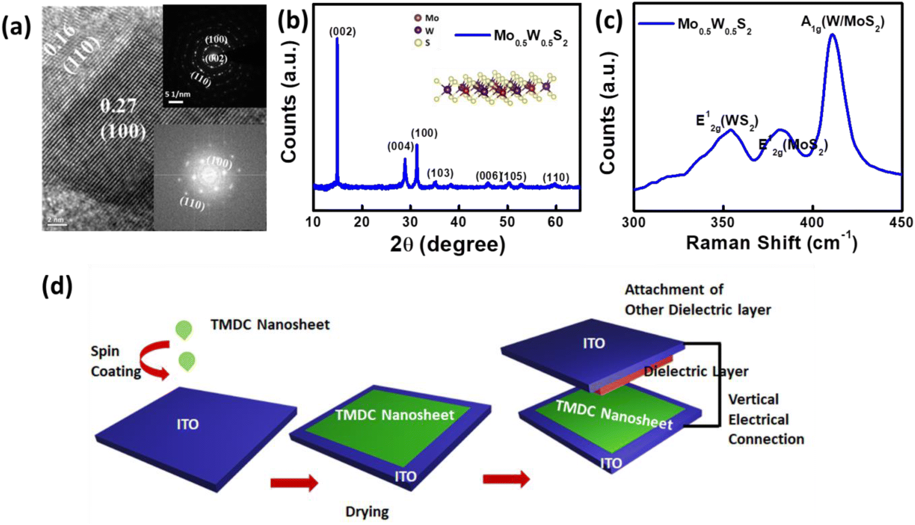 | ||
| Fig. 1 (a) High-resolution TEM image of the Mo0.5W0.5S2 nanosheet with interlayer spacings, with the inset showing the corresponding FFT and SAED patterns of the nanosheet. (b) XRD pattern of the Mo0.5W0.5S2 alloy nanosheet, with the schematic of the structure shown in the inset. (c) Typical Raman spectra of the alloy nanosheet at an excitation wavelength of ∼532 nm, with the indexed vibrational modes indexed. (d) Schematic steps for the fabrication of vertical-mode TENG devices. | ||
The knowledge of surface potential profile is very much important to understand the triboelectrification of semiconducting nanosheets. In this work, the surface potential profile of the TMDC ternary alloy nanosheets are examined by electrostatic force microscopy (EFM). From Fig. S6,† it is seen that the electrostatic potential is distributed over the whole nanosheet surface, necessary for the triboelectric contact electrification process.50 The schematic structure of the vertical mode TENG (V-TENG) device is depicted in Fig. 1d. Chemically synthesized TMDC alloy nanosheets (Mo0.5W0.5S2) are spin-coated onto a flexible ITO-PET substrate and used as active dielectric layers and another polymer layer on ITO acts as the second dielectric layer, which are separated by a spacer layer. The depicted working mechanism (Fig. 2a) of triboelectricity can be described into four consecutive steps: pressing, pressed, releasing, and released. When the polymer layer (nylon) and TMDC thin film layers are separated from each other and no external force is present, no triboelectric charges are generated on the friction layers (initial state), the electric potential difference between two triboelectric layer is zero, no charges flow in the external circuit, resulting in zero tribo-outputs. Upon the application of an external mechanical force, the two layers come into contact and equivalent opposite polarity tribocharges are generated in the surface of each layer. The previous equilibrium state breaks, leading to the generation of electrostatic charges on both sides of electrodes. The induced potential difference between the two electrodes drives the electrons to transfer from one electrode side to another through the external circuit, resulting in output voltage in the external circuit. When the external force is released from this TENG, the friction layers start to separate again, and then, the redistributed charges on each layer can build a reversed potential to drive the electrons to flow back in opposite directions, producing a reverse signal. The induced charges from the electrode flow in an opposite direction to screen out the induced electric potential difference between the two friction layers. When the applied force is completely removed, two friction layers are fully separated, and then, the TENG device is returned back to the original equilibrium state; thus, the four-step cycle of triboelectricity generation is completed. Individual V-TENG structures are fabricated by constructing different TENG pairs using a Mo0.5W0.5S2 thin film with different polymers, which gives a detailed idea about the contact electrification and surface charge polarity of Mo0.5W0.5S2 compared with other well-known triboelectric materials. Fig. 2b depicts the open circuit tribovoltage generation from each TENG pair (Mo0.5W0.5S2–PTFE and nylon) under pressing/releasing operations, and the output voltages switch its polarity in reverse connections for all TENG devices. A negative tribo-voltage is observed under pressing, and a positive signal is detected during the releasing action from the Mo0.5W0.5S2–PTFE structure, which is the opposite nature from the Mo0.5W0.5S2–nylon pair (Fig. 2b). It is confirmed that Mo0.5W0.5S2 is positively electrified during contact with PTFE. Other TENG structures (Mo0.5W0.5S2–PVDF, Mo0.5W0.5S2–PDMS, Mo0.5W0.5S2–PI, Mo0.5W0.5S2–PET, and Mo0.5W0.5S2–Mica) exhibit similar tribovoltage patterns (Fig. S7a†) to that of the Mo0.5W0.5S2–nylon pair, indicating that Mo0.5W0.5S2 is negatively electrified during contact with these polymers. These results reveal that the surface polarity of Mo0.5W0.5S2 is located in between PTFE and PVDF in the triboelectric series (depicted in Fig. 2c). Tribo-outputs depend on the relative polarity of two contact materials and also the charge transfer between the TMDC layer materials with the dielectric layer defined by their respective position in the tribo-series. When the dielectric is more tribo-positive (the tribo-positivity of these materials in the series being ordered as: PVDF < PDMS < PET < PI < mica < nylon),51 it is possible to generate higher tribo-voltage from that particular Mo0.5W0.5S2-dielectric pair, and accordingly, we obtained tribo-voltages from those different TENG device configurations (Fig. S7a†). The Mo0.5W0.5S2–nylon TENG pair can electrify Mo0.5W0.5S2 more negatively, as nylon is located at the positive side of triboelectric series, resulting in the generation of higher tribovoltage (Fig. 2d). Due to the periodic contact and separation, an alternating tribo-signal with peak-to-peak output voltage of ∼35 V is observed. The charge transfer mechanism between the 2D semiconducting material and dielectric insulators can be pictorialized by their work function differences (Fig. 2e). The work function difference leads to the generation of built-in-potential between the two contacting materials, and the electrons exchange to align the Fermi level. When the two materials are in contact, and if the semiconductor has a work function higher than that of the insulating polymer, then electrons will be transferred from the polymer to the semiconductor and vice versa.31 Despite the work function difference, the surface charge density and density of states have an impact on the direction and amount of transferred charges. In addition to the work function and polarity difference between the two contact layers; film thickness, surface roughness, surface contamination, and dielectric constant can influence the TENG output characteristics. The triboelectric current is generated not due to the motion of free charge carriers, but mainly due to displacement current, and hence, the displacement of tribo-layers defines the direction and amplitude of tribo-outputs, besides that the slight motion of bound charges of atoms and electric polarization of tribo materials contribute to tribo-outputs.52 To gain insights into the statistical distribution of the triboelectric outputs, ∼50 devices are prepared in identical configuration and open-circuit tribovoltage signals are tested under the same conditions (7.6 N), and the device-to-device average tribovoltage variation is depicted in Fig. S7b.† The open-circuit tribovoltage (Fig. S7c†) was observed to be up to ∼55 V (∓5 V) and the short circuit tribocurrent (Fig. S7d†) is estimated to be ∼165 nA (∓6 nA) under 56 N (0.56 MPa) external impact, revealing superior mechanical pressure tolerance of the TENG device. The vertical mode TENG generates output on the basis of vertical contact-separation between the semiconductor and dielectric layers and the open circuit voltage (Voc) is simulated using the COMSOL Multiphysics software, and the simulated output voltage (separation 14 mm) is plotted in Fig. 2f. As the surface charge density between two friction layers is influenced by the insulating spacer thickness in the TENG device, the tribovoltage is measured and simulated for different spacer thicknesses. The COMSOL simulation (Fig. S8a–c†) results indicate the potential distribution for different separation distances. The simulated potential distribution matches well with the experimental tribovoltage outputs, and the increase in separation distance between two friction layers results in an increase in potential differences, leading to the enhancement of tribovoltage (Fig. S8d†).
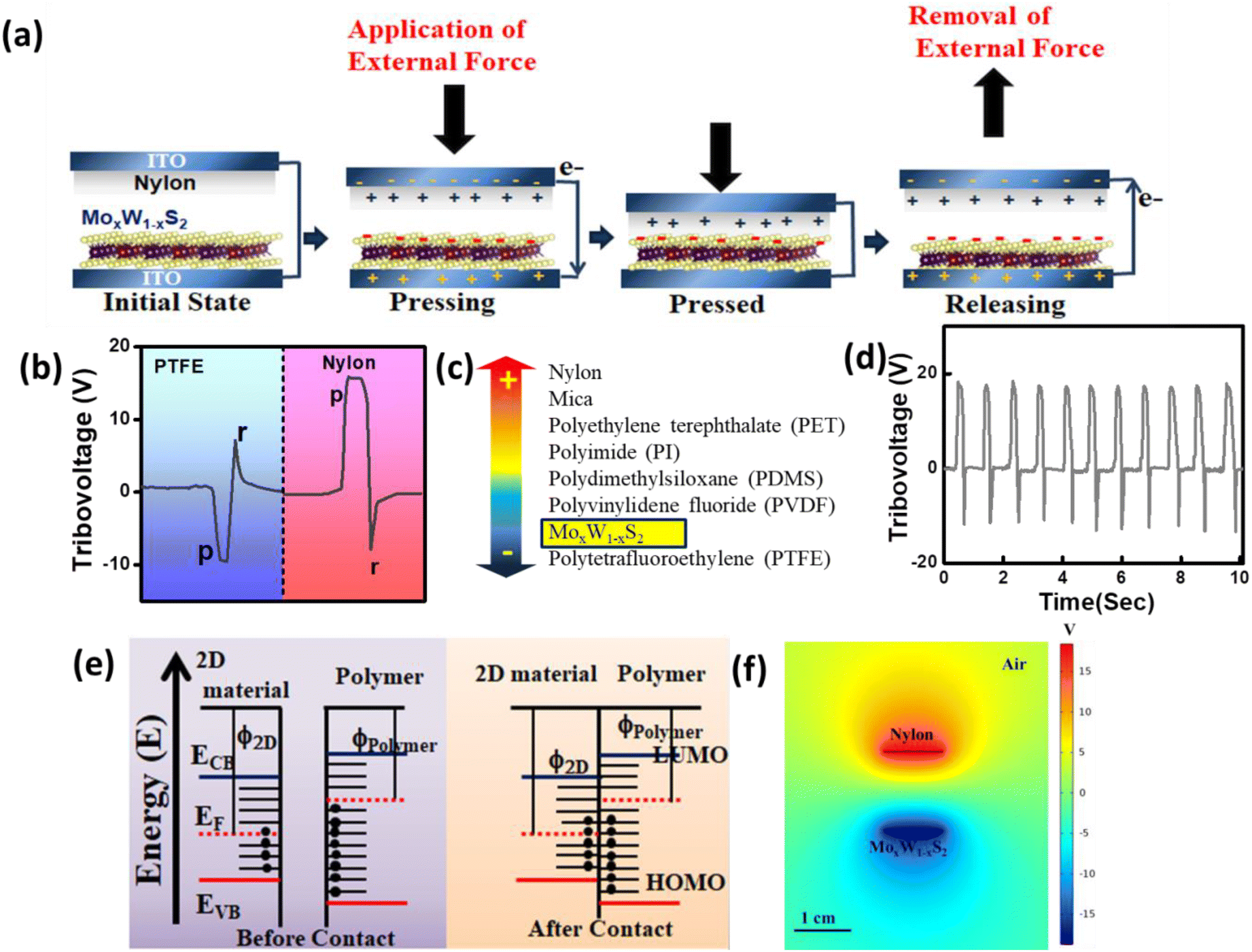 | ||
| Fig. 2 (a) Schematic working principle of the Mo0.5W0.5S2–nylon TENG devices operated under vertical pressing and releasing forces. (b) Triboelectric charging behaviour of Mo0.5W0.5S2 with PTFE and nylon (dielectric materials) and their corresponding open-circuit voltage, where p and r indicate the pressing and releasing actions. (c) Triboelectric charging polarity of Mo0.5W0.5S2 measured by pairing with the selected dielectric polymers and their position in triboelectric charging series. (d) Output voltage signal of a 2D Mo0.5W0.5S2 alloy nanosheet–nylon TENG. (e) Schematic of the working mechanism of contact charge transfer. (f) Triboelectric potential distribution simulated using the COMSOL Multiphysics software. | ||
The Mo0.5W0.5S2 ternary alloy–based two-terminal photodetector device exhibits a photoresponse superior to their binary counterparts (MoS2 and WS2). It is observed that for all the three devices under 410 nm LED illumination (∼325 μW cm−2 power), the photocurrent increases with the increase in bias voltages (Fig. S9a†), because of the enhanced drift velocity of charge carriers, excitation of photocarriers, separation, recombination and diffusion.53 The enhancement of photocurrent from the ternary alloy device is much higher than that of MoS2 and WS2 devices with a bias voltage caused by alloying (Mo0.5W0.5S2). Alloy formation supresses the large density of defect states than individual TMDCs, as well as it can covert the deep level defect to shallow levels.54,55 Therefore, for fabricating visible light energy harvesting TENG devices, the choice of TMDC ternary alloys is more appropriate than its binary counterparts. The potential of broadband photoresponse of the Mo0.5W0.5S2 ternary alloy-based device is examined by illuminating at different wavelengths, which cover almost the visible regime (365–633 nm) (Fig. S9b†). A model regarding the superiority of this ternary alloys is presented in Fig. S9c.† It is noticed that the photocurrent generated under blue (410 nm) illumination is slightly higher than that of the violet (365 nm) illumination, and much higher than that of green (535 nm) and red (633 nm) illumination, under a similar illumination intensity (Fig. 3a). It exactly correlates with the absorption spectrum of Mo0.5W0.5S2, due to enhanced absorption nearby the excition-C position, contributing higher photocurrents. Higher optical illuminations can produce larger numbers of photocarriers and generate more photocurrents.53,55 The work function mismatch between the tribo-layers (Mo0.5W0.5S2 ∼4.7 eV and nylon ∼4.08 eV) generates a built-in electric field, which can separate and accelerate the tribo charge carriers during the time of contact.52,56 At contact electrification under light illumination, photogenerated carriers (electron–hole) are produced in the TMDC layer, which can uplift the Fermi level in TMDCs,55 resulting in reduced work function mismatch between the two contact layers. It is easier for the photogenerated carriers to overcome this relatively less interfacial potential barrier, which causes the enhancement of tribo-photo coupled outputs.56,57 This mechanism of the photo-sensitive TENG is schematically depicted in Fig. 3b. To demonstrate the effect of superiority in the photoresponse of Mo0.5W0.5S2 ternary alloys over binary counterparts, three different TENG pairs are constructed using these three (MoS2, Mo0.5W0.5S2, and WS2) TMDC layers (under the same configuration), and tribo-outputs are measured under darkness and illumination. The schematic of the device is shown in Fig. 3c, with the experimental set up depicted in the inset. Fig. S10a and S10b† indicate that the photo-induced open circuit tribovoltage and short circuit tribocurrent are higher in ternary alloy–based TENG devices than in other TENG devices (410 nm, ∼525 μW cm−2 illumination). Upon illumination of visible light, photogenerated carriers in the TMDC layers are randomly scattered and recombined by the defect-mediated trap sites. Therefore, these recombined or scattered charges cannot be separated and exchanged with the dielectric layer, fail to generate charge carrier flow in the external circuit and cannot improve tribo-outputs. In case of the binary TMDC (MoS2, WS2), the major numbers of photogenerated carriers are trapped in S-vacancy-mediated defect states55 and cannot be added with the friction-mediated tribo-charges. The realignment of band positions and the suppression of defect states can enhance the charge carrier mobility in Mo0.5W0.5S2 ternary alloys, which is beneficial for the generation of higher photocurrents58 and the photocarriers are added with friction-induced tribo-charges, which can improve the photo-induced tribooutputs.59 Under illumination, the internal resistance of the TMDC semiconductor decreases, which effectively reduces the effective resistance of the TENG device, resulting in an easier way to flow the charge carriers.52 The impact force is an important parameter for controlling the triboelectric output; we tested the open circuit output voltage (Voc) and short circuit current (Isc) under variable applied forces. To examine the effect of light illumination, the tribo measurements are performed under dark and illuminated conditions (410 nm, ∼525 μW cm−2) and represented in Fig. 3d and e respectively. It is noticed that under dark conditions, Voc is increased monotonically from 2.8 V to 17.2 V with the increase in applied force from 1.2 N to 7.6 N and Isc is enhanced from 0.8 nA (1.2 N) to 4.1 nA (7.6 N). Under illuminated conditions and for 7.6 N applied force, Voc is enhanced by 61% and Isc is increased by 253% compared with those under dark conditions. The voltage sensitivity is improved from 2.54 V N−1 (dark) to 3.58 V N−1 (light), and similarly, current sensitivity is also enhanced from 0.51 nA N−1 (dark) to 1.89 nA N−1 (light). Under illuminated conditions, photo-induced e–h pairs are generated, which can enhance the effective carrier density in Mo0.5W0.5S2, contact electrification-induced internal electric field and Fermi level modulation in semiconducting layers, can enhance the exchange of charges. This modulated charge transfer mechanism in semiconductor–nylon polymers leads to higher current and voltage outputs. It is important to be noted that the photo-coupled tribo performance of this reported TENG is much higher than the previously reported photosensitive TENGs.60–63 The temporal outputs Voc and Isc were measured under darkness and under illumination at different wavelengths (365 nm, 410 nm, 535 nm, and 633 nm), which are depicted in Fig. 3f and g, indicating the promising energy harvesting ability throughout the broadband regime. It is estimated that Voc shows 50.3% (365 nm, 546 μW cm−2), 61% (410 nm, 525 μW cm−2), 42.4% (535 nm, 490 μW cm−2), and 34.8% (633 nm, 530 μW cm−2) enhancement compared with that under darkness and Isc shows 240%, 253%, 124%, and 104% enhancement respectively. This relatively high photo-coupled triboelectric outputs under blue light (410 nm) than violet (365 nm), green (535 nm), and red (633 nm) illuminations are attributed to the presence of higher density of photo-excited carriers,64,65 which can be correlated with the absorption spectrum and photocurrent characteristics of Mo0.5W0.5S2.
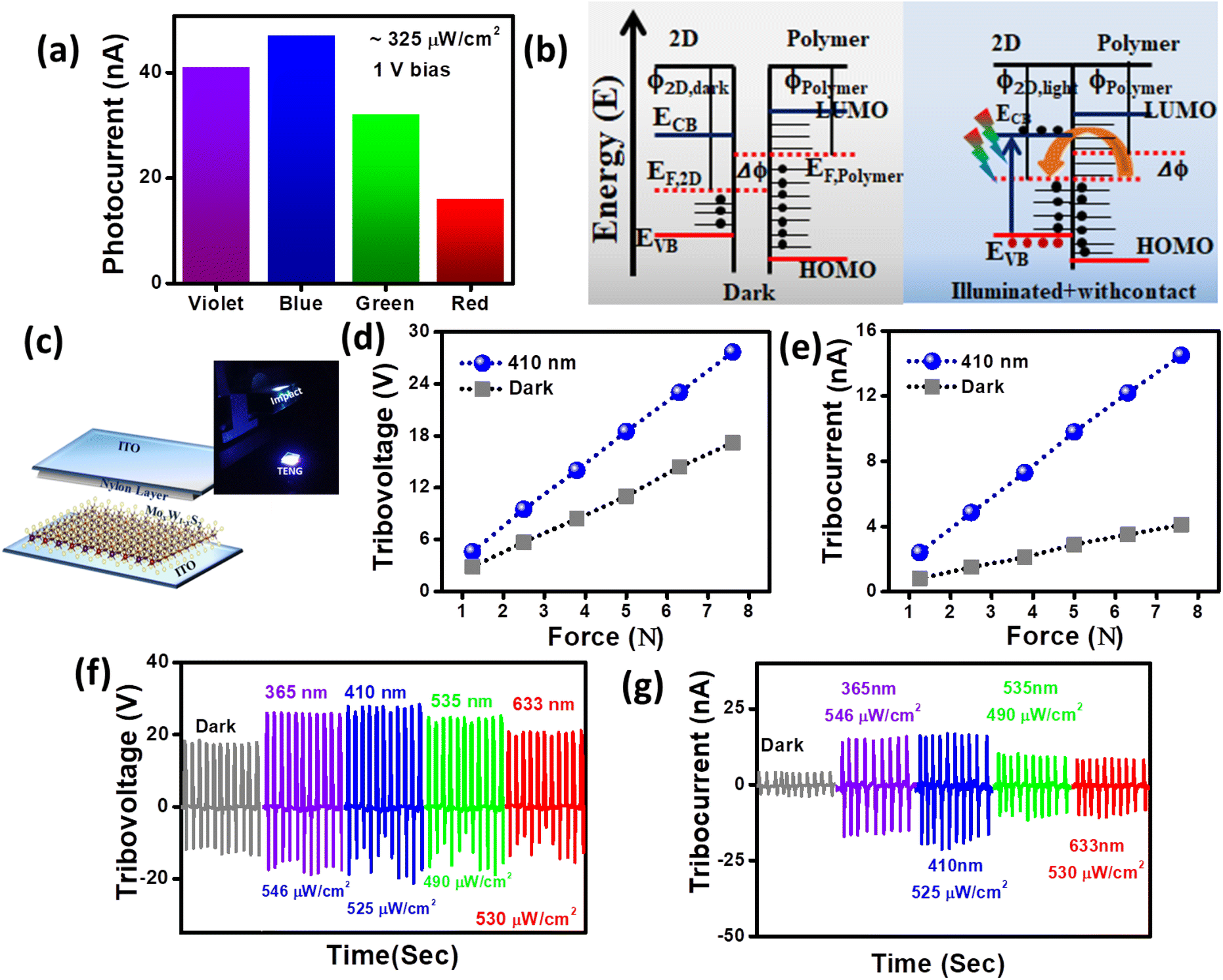 | ||
| Fig. 3 (a) Variation in photocurrents from Mo0.5W0.5S2 nanosheets under illumination at 365, 410, 535 and 633 nm in two-terminal device configurations. (b) Schematic working mechanism of the vertical TENG device under dark and illuminated conditions. (c) Schematic of the V-TENG device, with the image of the experimental set up shown in the inset. Variations of (d) open circuit tribovoltage and (e) short circuit tribocurrent of the Mo0.5W0.5S2–nylon V-TENG device under dark and illuminated conditions (410 nm) as a function of applied force. Output performance of the TENG device: (f) open circuit voltage and (g) short circuit current under darkness and illumination at 365, 410, 535 and 633 nm (7.6 N applied force). | ||
As the photosensitive Mo0.5W0.5S2 friction layer has strong absorbance in the blue region of the spectra and also the TENG device generates higher tribo-outputs under 410 nm, power-dependent tribo measurements are carried out under constant impact force (7.6 N) with 410 nm illumination. From Fig. 4a and b, it is observed that Voc is increased from 21.4 to 27.7 V and Isc is enhanced amplitude from 7.1 to 14.5 nA with the increase in illumination intensity from ∼120 to ∼525 μW cm−2. Withdrawing the illumination, tribo amplitudes recover to the state as darkness even under repeated light on/off cyclic conditions. The device exhibits outstanding durability in photoresponse, and such advantage can be used to fabricate self-powered, ultralow illumination sensors with real-time monitoring. The illumination intensity generated an enhanced number of photogenerated carriers (Fig. S9b†), improving the triboelectric outputs66 of this V-TENG device. The overall short circuit tribo-current is increased gradually with the increase in illumination power for all wavelengths (Fig. S11†), indicating the variation in light-induced tribocurrent with illumination intensity. The enhancement of photo-enhanced tribo-voltage (Vlight–Vdark) and tribo-current (Ilight–Idark) with illumination power at different wavelengths (365, 410, 535, and 633 nm) is depicted in Fig. 4c and d, and from this, we estimate the voltage responsivity, defined as 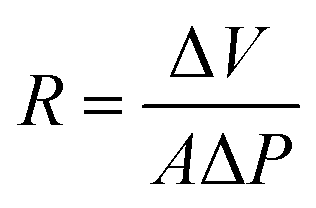 of the TENG,63 which is 42.2, 45.5, 27.85, and 13.51 V mW−1 under 365, 410, 535, and 633 nm illumination respectively (Fig. 4e), (where ΔV is the change in voltage amplitude under illumination, ΔP is the incident power and A is the effective area of the device). The estimated values of current responsivity are 14.8, 17.0, 12.4 and 11.1 nA mW−1 respectively, under 365, 410, 535, and 633 nm illumination conditions. This reported voltage sensitivity is higher than that of the previously reported photosensitive TENGs,60,63–65 and the superiority of this fabricated TENG device is represented in Table 1. Here ultralow illumination power acts as control on tribo outputs, and hence, this TENG device shows potential in fabricating self-powered photosensitive flexible nano-micro devices. The effect of illumination on the energy harvesting performance is examined by measuring the output power from the TENG device across different load resistances (under constant impact 7.6 N and 410 nm, 525 μW cm−2). It is found that the TENG exhibits 13.25 μW cm−2 areal power density under illuminated conditions, which is 2.72 times higher than that under darkness (Fig. 4f). It is estimated that the power density is enhanced by 172% compared with that under darkness, and the comparative performance of this TENG is depicted in Table 1. Thus, the enhancement of power generation capability under this low illumination implies superior photo-mechanical coupled energy harvesting potential to those reported previously.66–69 The fabricated TENG exhibits highly stable tribo-output even after 3 months of fabrication (Fig. S12a†), and exhibits superior flexibility (Fig. S12b and c†), making it attractive for prototyping and commercialization.
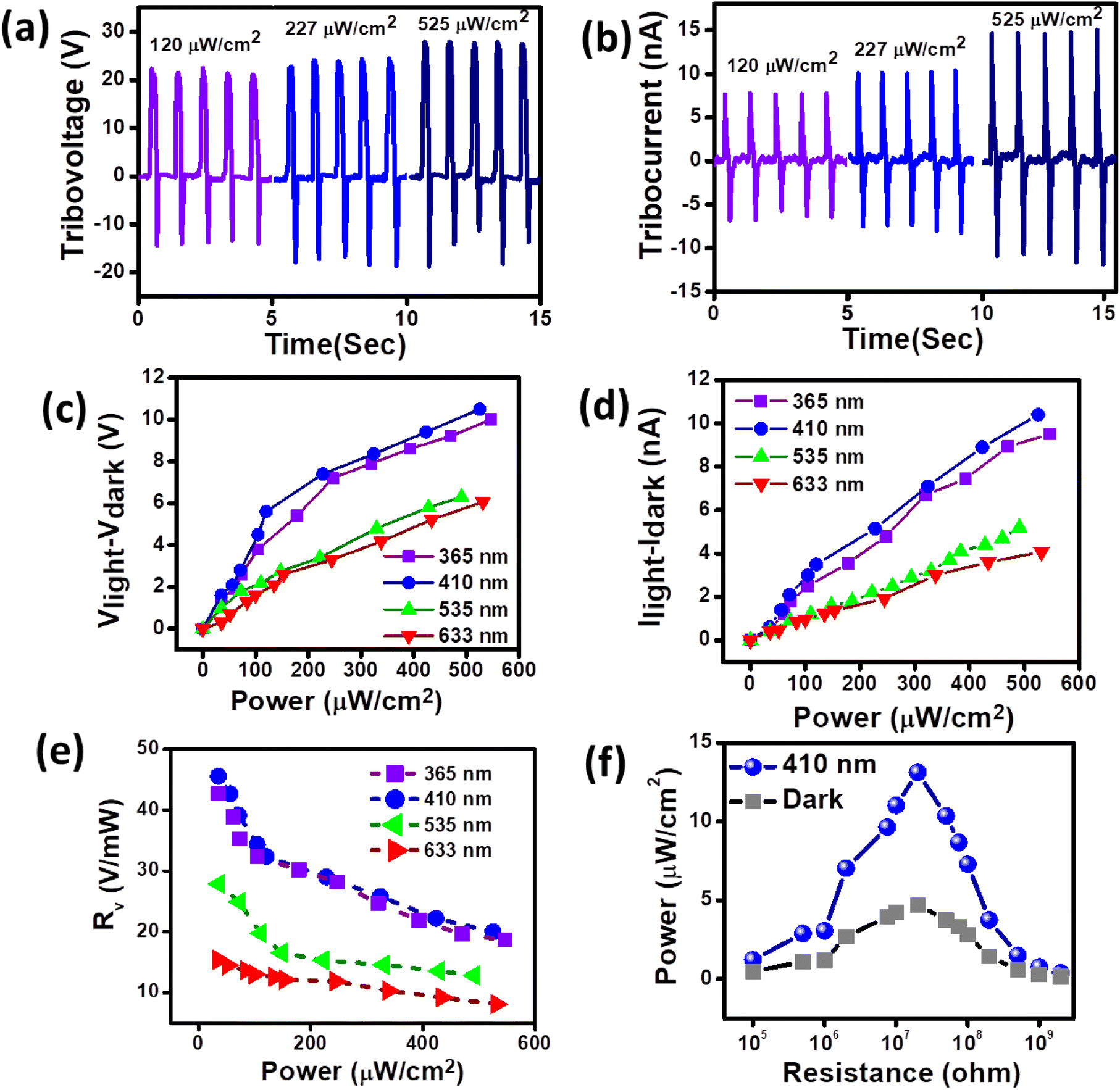 | ||
| Fig. 4 Variation in (a) open circuit voltage and (b) short circuit current from the Mo0.5W0.5S2–nylon V-TENG device under different illumination intensities (410 nm). The variation in photo-induced (c) tribovoltage and (d) tribocurrent with illumination power at 365 nm, 410 nm, 535 nm and 633 nm wavelengths. (e) Variation in responsivity (in voltage mode) with illumination power under different illumination wavelengths. (f) Output power density from the V-TENG device under different load resistances under dark and illuminated conditions. | ||
| Materials | Tribo-output | Responsivity | Power enhancement (%) | Ref. |
|---|---|---|---|---|
| MAPbI3 + TiO2 | 17 V | 4.25 × 0−3 V mW−1 | — | 59 |
| PDMS/Mxenes–Ag NW | 145 V | 17.91 V mW−1 | 414 | 66 |
| Bismuth oxyhalide | 45.4 V | 0.04 × 0−3 V mW−1 | 76 | 67 |
| MAPbI3 + TiO2 nanoparticle | 4 V | 7.6 × 0−3 V mW−1 | — | 63 |
ZnO–P3HT![[thin space (1/6-em)]](https://www.rsc.org/images/entities/char_2009.gif) :PC61BM nanocomposite :PC61BM nanocomposite |
7 V | 0.108 V mW−1 | — | 65 |
| CsBi3I10 | 80 V | 20 V mW−1 | 28.23 | 69 |
| MAPbIxCl3−x–TiO2 | 22.8 V | 0.036 V mW−1 | 73.10 | 64 |
| Mo 0.5 W 0.5 S 2 | 27.8 V | 45.5 V mW −1 | 172 | This study |
Finally, the output performance of the TENG was investigated for various practical applications. The external impact is a very crucial parameter to control tribo-outputs; from Fig. 5a, it is observed that Voc is increased from 0.65 V to 8.05 V linearly with the increase in impact force from 0.2 to 4 N. Under very low impact, this TENG exhibits superior sensitivity 3.54 V N−1, but the sensitivity falls with increase in applied impact. The flexible TENG device can be attached with different parts of the human body, and upon movement of parts such as wrist, arms, and elbow, the TENG generates a noticeable open circuit output voltage (Fig. 5b–d) and the magnitude of the tribovoltage remains unchanged even after multitude of repetitive cycles. This TENG is attached with five finger joint positions and the bending of each joint at different angle produces open circuit tribovoltage (Fig. 5e), making it a promising candidate for next-generation wearable energy harvesting devices. As repeated mechanical impact on the TENG can produce open circuit output voltages, mechanical to electrical energy conversion efficiency can be utilized to store the charge, which can power up various electronic devices. Fig. 5f indicates that this TENG is able to charge a 1.2 μF capacitor up to 17 V within a very short time (∼16 s), which can lit up commercial LED devices. The touch response of the TENG can be verified by fabricating a 3 × 3 pixel array in a planar configuration. The touch response of this pixel array in the form of discrete area is pictorially represented in Fig. 5g, such that pressing by fingertip at a particular pixel generates voltage at that particular one and the recorded voltage is depicted by a bar plot. This 3 × 3 pixel array-based TENG can be attached to the human body/any curved area and can act as touch-sensitive artificial e-skin with mild pressing. The demonstrated experimental results indicate the superiority of the fabricated self-powered TENGs, which possess a great potential for application in next-generation flexible, wearable and portable devices.
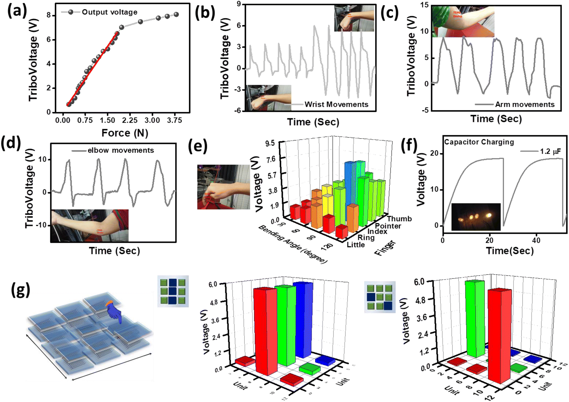 | ||
| Fig. 5 (a) Variation in open circuit tribovoltage from the TENG device under a low-impact force. Generation of open circuit output voltage due to the movement of (b) wrist, (c) arms, (d) elbow, and (e) five fingers at different bending angles. (f) Charging of a capacitor and glowing of an LED in the self-powered mode. (g) Schematic demonstration of touch sensitivity of this TENG in the pixel array format, different patterned output voltage is depicted and the corresponding patterned impact is shown in the inset. | ||
3. Conclusion
In summary, we have demonstrated visible light energy harvesting TENG devices using 2D semiconducting ternary alloy (Mo0.5W0.5S2) nanosheets with enhanced photo-coupled triboelectric outputs. The open circuit tribovoltage and short circuit tribocurrent exhibit giant enhancement of 61% and 253% respectively under visible light illumination (410 nm, 525 μW cm−2) compared to their dark counterparts. The power harvesting ability can also be enhanced (with an areal power density ranging from 4.8 to 13.25 μW cm−2) under the same condition. The TENG device exhibits superior photoresponsivities of 42.2, 45.5, 28 and 15.4 V mW−1 under 365, 410, 535, and 633 nm illuminations, respectively, demonstrating the energy harvesting capability even under very low light intensity throughout the visible range. The enhanced performance under illumination is due to the higher density of photogenerated charge carriers, which causes the enhancement of effective surface charge density of triboelectric layers and improves the charge exchange between two contact layers. The demonstrated results confirm that this fabricated flexible TENG is a promising candidate for mechanical-photo coupled energy harvesting and self-powered photosensitive sensors. The capacitor charging and energy harvesting from regular human activities indicate the potential of the TENG for driving portable electronic devices. Versatile, self-powered, durable, multi-functional, and photosensitive TENGs can be attractive as sustainable energy resources, and are highly promising for next-generation portable, optoelectronic sensors.4. Experimental section
Materials and reagents
Sodium molybdate dihydrate (Na2MoO4·2H2O), sodium tungstate dihydrate, (Na2WO4·2H2O), and thiourea (CH4N2S) were purchased from Alpha Aesar. Polyvinylidene fluoride (PVDF), polydimethylsiloxane (PDMS), and polyethylene terephthalate (PET) were bought from Sigma Aldrich. Polytetrafluoroethylene (PTFE), Kapton (polyimide) and nylon were commercially available.Synthesis
Mo0.5W0.5S2 ternary alloy nanosheets along with binary counterparts were synthesized by a sonochemical-assisted hydrothermal synthesis technique.42 The black precipitate obtained from the hydrothermal autoclave was washed thoroughly and kept for drying. The power was dissolved in an IPA solvent and kept in a bath sonicator to get the nanosheet morphology, and the unexfoliated bulk part was removed by centrifugation.Fabrication of TENG devices
The exfoliated TMDC nanosheets (5 mg ml−1) were spin-coated onto the 1 × 1 cm2 ITO side of an ITO–PET substrate to prepare the TMDC thin film and kept on a hot plate for drying. To prepare the transparent nylon film on the ITO substrate, the first nylon solution was extracted in an acetone solvent and spin-coated onto the top of the ITO substrate. These two layers were separated by a spacer, and here, the TMDC and nylon film act as negative and positive tribo friction layers respectively. Silver paste and copper wires were connected with flexible ITO electrodes.Fabrication of two-terminal photodetectors
Photodetector devices were fabricated by using PET as the flexible substrate. First, PET substrates were cleaned several times with acetone and IPA. Then, a thin layer of gold was deposited (∼50 nm) by using a metal shadow mask via e-beam deposition. The space between the electrodes was maintained at ∼25 μm. The exfoliated TMDC nanosheets (5 mg ml−1) were then drop-casted to make complete photodetector devices. Finally, the whole system was dried in a hot plate at ∼80 °C for 2 hours.Characterizations
The scanning electron microscopy (SEM) along with energy-dispersive X-ray (E-DAX) measurements was performed using a field emission SEM system with 25 keV beam energy at 4 mm distance under low vacuum. To study the morphology and inter planer spacings in detail, transmission electron microscopy (TEM) and selected area electron diffraction (SAED) measurements were performed using an FEG source at 200 kV. The phase and crystallinity of the exfoliated nanosheets were measured by X-ray diffraction (Rigaku (Smartlab)) with a 40 kV energy source. The surface profiles and morphology of the nanosheets were examined by atomic force microscopy (AFM), and the surface potential profile was measured by electrostatic force microscopy (EFM) in the lift mode using an AFM set-up. Conductive-AFM (C-AFM) measurements on the TMDC friction layers were performed using a Pt–Ir-coated Si tip in the contact mode and a UV-Vis spectrometer (Shimadzu UV-Vis 2600 Spectrophotometer) was used to record the absorption spectra of the synthesized nanosheets and micro-Raman and photoluminescence spectra were recorded using a spectrometer (LabRam HR Evolution; HORIBA France SAS-532 nm laser). The open circuit tribovoltage and short circuit tribocurrent from the TENG device and current–voltage characteristics of the two-terminal photodetectors were measured using a Keithley 2450 source meter with the Kickstart software. Thorlab LEDs (365, 410, 535, and 633 nm) were employed as the optical illumination source, and they were calibrated using a spectrometer coupled with an integrating sphere (Flame-Ocean optics).Simulation
The open circuit voltage from this V-TENG device was investigated using the COMSOL-Multiphysics 5.5 simulation software in the electrostatic module. The potential difference is governed by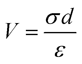 , where σ denotes the surface charge density, d is the spacer layer thickness and ε is the dielectric constant. Here, the top surface is a nylon layer and the bottom surface is a TMDC layer, which are positive and negative triboelectric layers respectively.
Conflicts of interest
There are no conflicts to declare.Acknowledgements
D. B. acknowledges Dr Avijit Chowdhury for arranging her research fellowship (Bridge Fellowship, S. N. Bose National Centre for Basic Sciences). S. M. acknowledges the INSPIRE Fellowship program, DST, Govt. of India, for providing him research fellowship (IF170929). S. K. R. acknowledges his INAE chair professor award. We all acknowledge Dr Sayan Bayan for his scientific contributions. All the authors acknowledge Dr Atindra Nath Pal for his scientific inputs.References
- X. Yang, G. Liu, Q. Guo, H. Wen, R. Huang, X. Meng, J. Duan and Q. Tang, Nano Energy, 2022, 92, 106757 CrossRef CAS
.
- T. Bu, T. Xiao, Z. Yang, G. Liu, X. Fu, J. Nie, T. Guo, Y. Pang, J. Zhao, F. Xi, C. Zhang and Z. L. Wang, Adv. Mater., 2018, 30, 1–8 Search PubMed
- T. Liu, M. Liu, S. Dou, J. Sun, Z. Cong, C. Jiang, C. Du, X. Pu, W. Hu and Z. L. Wang, ACS Nano, 2018, 12, 2818–2826 CrossRef CAS PubMed
- C. Wu, A. C. Wang, W. Ding, H. Guo and Z. L. Wang, Adv. Energy Mater., 2019, 9, 1–25 Search PubMed
- A. Yu, X. Chen, R. Wang, J. Liu, J. Luo, L. Chen, Y. Zhang, W. Wu, C. Liu, H. Yuan, M. Peng, W. Hu, J. Zhai and Z. L. Wang, ACS Nano, 2016, 10, 3944–3950 CrossRef CAS PubMed
- L. Gu, N. Cui, L. Cheng, Q. Xu, S. Bai, M. Yuan, W. Wu, J. Liu, Y. Zhao, F. Ma, Y. Qin and Z. L. Wang, Nano Lett., 2013, 13, 91–94 CrossRef CAS PubMed
- D. Bhattacharya, S. Bayan, R. K. Mitra and S. K. Ray, ACS Appl. Electron. Mater., 2020, 2, 3327–3335 CrossRef CAS
- D. Bhattacharya, S. Bayan, R. K. Mitra and S. K. Ray, Nanoscale, 2021, 13, 15819–15829 RSC
- S. Bayan, D. Bhattacharya, R. K. Mitra, S. K. Ray and S. K. Ray, Nanotechnology, 2020, 31, 365401 CrossRef CAS PubMed
- Z. L. Wang, Faraday Discuss., 2014, 176, 447–458 RSC
- L. Lin, Y. Xie, S. Wang, W. Wu, S. Niu, X. Wen and Z. L. Wang, ACS Nano, 2013, 7, 8266–8274 CrossRef CAS PubMed
- P. Wu, F. Wang, S. Xu, Y. Liu, X. Zhao, C. Zhang and X. Mu, Adv. Sci., 2023, 10, 2301199 CrossRef PubMed
- X. Chen, F. Wang, Y. Zhao, P. Wu, L. Gao, C. Ouyang, Y. Yang and X. Mu, Research, 2022, 2022, 9765634 CAS
- C. Zhang, L. M. Zhang, W. Tang, C. B. Han and Z. L. Wang, Adv. Mater., 2015, 27, 3533–3540 CrossRef CAS PubMed
- W. Ding, A. C. Wang, C. Wu, H. Guo and Z. L. Wang, Adv. Mater. Technol., 2019, 4, 1–16 Search PubMed
- Y. Pang, F. Xue, L. Wang, J. Chen, J. Luo, T. Jiang, C. Zhang and Z. L. Wang, Adv. Sci., 2015, 3, 1–8 Search PubMed
- S. Mukherjee, D. Bhattacharya, S. Patra, S. Paul, R. K. Mitra, P. Mahadevan, A. N. Pal and S. K. Ray, ACS Appl. Mater. Interfaces, 2022, 14, 5775–5784 CrossRef CAS PubMed
- D. Bhattacharya, S. Mukherjee, R. K. Mitra and S. K. Ray, Nanotechnology, 2020, 31, 1–9 CrossRef PubMed
- J. Meng, H. Li, L. Zhao, J. Lu, C. Pan, Y. Zhang and Z. Li, Nano Lett., 2020, 20, 4968–4974 CrossRef CAS PubMed
- Y. Zhang, M. Peng, Y. Liu, T. Zhang, Q. Zhu, H. Lei, S. Liu, Y. Tao, L. Li, Z. Wen and X. Sun, ACS Appl. Mater. Interfaces, 2020, 12, 19384–19392 CrossRef CAS PubMed
- L. Wang, Y. Wang, H. Wang, G. Xu, A. Döring, W. A. Daoud, J. Xu, A. L. Rogach, Y. Xi and Y. Zi, ACS Nano, 2020, 14, 10359–10369 CrossRef CAS PubMed
- D. Zhang, Z. Xu, Z. Yang and X. Song, Nano Energy, 2020, 67, 104251 CrossRef CAS
- Z. Wen, J. Fu, L. Han, Y. Liu, M. Peng, L. Zheng, Y. Zhu, X. Sun and Y. Zi, J. Mater. Chem. C, 2018, 6, 11893–11902 RSC
- S. Ippili, V. Jella, S. Eom, S. Hong and S. G. Yoon, ACS Appl. Mater. Interfaces, 2020, 12, 50472–50483 CrossRef CAS PubMed
- V. Nguyen and R. Yang, Nano Energy, 2013, 2, 604–608 CrossRef CAS
- C. Wu, A. C. Wang, W. Ding, H. Guo and Z. L. Wang, Adv. Energy Mater., 2019, 9, 1802906 CrossRef
- H. Ryu, J. H. Lee, T. Y. Kim, U. Khan, J. H. Lee, S. S. Kwak, H. J. Yoon and S. W. Kim, Adv. Energy Mater., 2017, 7, 1–6 Search PubMed
- L. Gao, X. Chen, S. Lu, H. Zhou, W. Xie, J. Chen, M. Qi, H. Yu, X. Mu, Z. L. Wang and Y. Yang, Adv. Energy Mater., 2019, 9, 1–11 Search PubMed
- S. Kim, M. K. Gupta, K. Y. Lee, A. Sohn, T. Y. Kim, K. S. Shin, D. Kim, S. K. Kim, K. H. Lee, H. J. Shin, D. W. Kim and S. W. Kim, Adv. Mater., 2014, 26, 3918–3925 CrossRef CAS PubMed
- C. Zhang and Z. L. Wang, Nano Today, 2016, 11, 521–536 CrossRef CAS
- M. Seol, S. Kim, Y. Cho, K. E. Byun, H. Kim, J. Kim, S. K. Kim, S. W. Kim, H. J. Shin and S. Park, Adv. Mater., 2018, 30, 1–8 Search PubMed
- T. I. Kim, I. J. Park, S. Kang, T. S. Kim and S. Y. Choi, ACS Appl. Mater. Interfaces, 2021, 13, 21299–21309 CrossRef CAS PubMed
- C. Wu, T. W. Kim, J. H. Park, H. An, J. Shao, X. Chen and Z. L. Wang, ACS Nano, 2017, 11, 8356–8363 CrossRef CAS PubMed
- M. Chhowalla, H. S. Shin, G. Eda, L. J. Li, K. P. Loh and H. Zhang, Nat. Chem., 2013, 5, 263–275 CrossRef PubMed
- Q. H. Wang, K. Kalantar-Zadeh, A. Kis, J. N. Coleman and M. S. Strano, Nat. Nanotechnol., 2012, 7, 699–712 CrossRef CAS PubMed
- D. Bhattacharya, S. Mukherjee, R. K. Mitra and S. K. Ray, IOP Nanotechnol., 2023, 34, 435401 CrossRef PubMed
- S. Mukherjee, D. Bhattacharya, S. K. Ray and A. N. Pal, arXiv, 2022, 1–30 Search PubMed
- S. Mukherjee, D. Bhattacharya, S. K. Ray and A. N. Pal, ACS Appl. Mater. Interfaces, 2022, 14, 34875–34883 CrossRef CAS PubMed
- J. H. Yang and B. I. Yakobson, Chem. Mater., 2018, 30, 1547–1555 CrossRef CAS
- B. Huang, M. Yoon, B. G. Sumpter, S. H. Wei and F. Liu, Phys. Rev. Lett., 2015, 115, 1–5 Search PubMed
- H. P. Komsa and A. V. Krasheninnikov, J. Phys. Chem. Lett., 2012, 3, 3652–3656 CrossRef CAS PubMed
- D. Bhattacharya, S. Mukherjee, A. N. Pal, R. K. Mitra and S. K. Ray, Adv. Opt. Mater., 2022, 10, 2200353 CrossRef CAS
- S. Arulkumar, S. Parthiban, A. Goswami, R. S. Varma, M. Naushad and M. B. Gawande, Mater. Res. Express, 2019, 6(12), 125019 CrossRef
- W. Li, F. Li, Y. Liu, J. Li, H. Huo and R. Li, Int. J. Hydrogen Energy, 2017, 42, 18774–18784 CrossRef CAS
- Y. Lei, S. Pakhira, K. Fujisawa, X. Wang, O. O. Iyiola, N. Perea López, A. Laura Elías, L. Pulickal Rajukumar, C. Zhou, B. Kabius, N. Alem, M. Endo, R. Lv, J. L. Mendoza-Cortes and M. Terrones, ACS Nano, 2017, 11, 5103–5112 CrossRef CAS PubMed
- N. Mutz, T. Meisel, H. Kirmse, S. Park, N. Severin, J. P. Rabe, E. List-Kratochvil, N. Koch, C. T. Koch, S. Blumstengel and S. Sadofev, Appl. Phys. Lett., 2021, 118, 013102 CrossRef
- A. F. Rigosi, H. M. Hill, K. T. Rim, G. W. Flynn and T. F. Heinz, Phys. Rev. B, 2016, 94, 1–6 CrossRef
- Y. Chen, J. Xi, D. O. Dumcenco, Z. Liu, K. Suenaga, D. Wang, Z. Shuai, Y. S. Huang and L. Xie, ACS Nano, 2013, 7, 4610–4616 CrossRef CAS PubMed
- J. Liu, A. Goswami, K. Jiang, F. Khan, S. Kim, R. McGee, Z. Li, Z. Hu, J. Lee and T. Thundat, Nat. Nanotechnol., 2018, 13, 112–116 CrossRef CAS PubMed
- R. Sanikop, N. Arya, V. Balakrishnan and C. Sudakar, J. Phys. Chem. C, 2021, 125, 12155–12165 CrossRef CAS
- Y. Liu, J. Mo, Q. Fu, Y. Lu, N. Zhang, S. Wang and S. Nie, Adv. Funct. Mater., 2020, 30, 2004714 CrossRef CAS
- Y. Wang, X. Yang, X. Yu, J. Duan, Q. Yang, Y. Duan and Q. Tang, Nano Energy, 2020, 77, 105280 CrossRef CAS
- Y. R. Lim, J. K. Han, Y. Yoon, J. B. Lee, C. Jeon, M. Choi, H. Chang, N. Park, J. H. Kim, Z. Lee, W. Song, S. Myung, S. S. Lee, K. S. An, J. H. Ahn and J. Lim, Adv. Mater., 2019, 31, 1–14 Search PubMed
- H. Yu, H. Yan, H. Li, Z. Li, Y. Bai, H. Zhu and S. Yin, ACS Appl. Mater. Interfaces, 2021, 13, 44693–44702 CrossRef CAS PubMed
- J. Yao, Z. Zheng and G. Yang, ACS Appl. Mater. Interfaces, 2016, 8, 12915–12924 CrossRef CAS PubMed
- Q. Guo, X. Yang, Y. Wang, W. Xu, J. Duan and Q. Tang, Adv. Funct. Mater., 2021, 31, 1–11 Search PubMed
- S. Lin, L. Xu, L. Zhu, X. Chen and Z. L. Wang, Adv. Mater., 2019, 31, 1–8 Search PubMed
- H. Yu, H. Yan, H. Li, Z. Li, Y. Bai, H. Zhu and S. Yin, ACS Appl. Mater. Interfaces, 2021, 13, 44693–44702 CrossRef CAS PubMed
- L. Su, Z. Zhao, H. Li, Y. Wang and S. Kuang, J. Mater. Chem. C, 2016, 4, 10395–10399 RSC
- S. Bayan, D. Bhattacharya, R. K. Mitra and S. K. Ray, Nanoscale, 2020, 12, 21334–21343 RSC
- H. Guan, D. Lv, T. Zhong, Y. Dai, L. Xing and X. Xue, Nano Energy, 2020, 67, 104182 CrossRef CAS
- Y. Dai, Y. Fu, H. Zeng, L. Xing, Y. Zhang, Y. Zhan and X. Xue, Adv. Funct. Mater., 2018, 1800275, 1–9 Search PubMed
- L. Su, Z. X. Zhao, H. Y. Li, J. Yuan, Z. L. Wang and G. Z. Cao, ACS Nano, 2017, 11, 8356–8363 CrossRef PubMed
- X. De Yang, J. J. Han, G. Wang, L. P. Liao and C. Y. Xu, J. Mater. Sci., 2019, 54, 9004–9016 CrossRef
- Y. W. Mingqing Li, L. Yang, H. Wang, C. Qin, J. Song, Y. Zhang, W. Wang and H. Z. Xinan Zhang, Appl. Phys. Lett., 2021, 119, 063903 CrossRef
- Y. Liu, E. Li, Y. Yan, Z. Lin, Q. Chen, X. Wang, L. Shan, H. Chen and T. Guo, Nano Energy, 2021, 86, 106118 CrossRef CAS
- Z. Yu, H. Yang, N. Soin, L. Chen, N. Black, K. Xu, P. Kumar, C. Tsonos, A. Kumar and J. Luo, Nano Energy, 2021, 89, 106419 CrossRef CAS
- G. Pace, M. Serri, A. E. D. R. Castillo, A. Ansaldo, S. Lauciello, M. Prato, L. Pasquale, J. Luxa, V. Mazánek, Z. Sofer and F. Bonaccorso, Nano Energy, 2021, 87, 106173 CrossRef CAS
- Z. Wei, L. Ding, N. Sun, L. Y. Dang, H. R. Sun, J. C. Han, J. Q. Zhu and G. G. Wang, Nano Energy, 2023, 108, 108209 CrossRef CAS
Footnote |
| † Electronic supplementary information (ESI) available. See DOI: https://doi.org/10.1039/d3nr02791k |
| This journal is © The Royal Society of Chemistry 2023 |