
Crystal photonics foundry: geometrical shaping of molecular single crystals into next generation optical cavities†
Vuppu Vinay
Pradeep
 a,
Melchi
Chosenyah
a,
Evgeniy
Mamonov
*b and
Rajadurai
Chandrasekar
*a
a,
Melchi
Chosenyah
a,
Evgeniy
Mamonov
*b and
Rajadurai
Chandrasekar
*a
aSchool of Chemistry and Centre for Nanotechnology, University of Hyderabad, Prof. C. R. Rao Road, Gachibowli, Hyderabad 50046, India. E-mail: r.chandrasekar@uohyd.ac.in
bDepartment of Physics, Quantum Electronics Division, Moscow State University, Moscow 119991, Russia. E-mail: mamonov@shg.ru
First published on 28th June 2023
Abstract
The advancements in organic photonics have reached new heights in the recent past with the demonstration of diverse organic crystal optical components and circuits. However, the development of industrially viable manufacturing of organic optical components is the need of the hour for finding an alternative to silicon-based photonics. Here, we demonstrate focused ion beam (FIB) milling as a tool to shape organic single crystals into optical cavities of diverse geometries and dimensions. The generality of FIB milling was tested on perylene and coumarin-153 microcrystals. The microcrystals obtained by self-assembly of perylene and sublimation of coumarin-153 were carved into desired disc-, ring- and rectangular shapes. These shaped crystals act as cavities exhibiting sharp resonance modes in the fluorescence spectrum, confirming optical interference. The FDTD numerical calculations support the light electric field distribution in these optical cavities. This unprecedented single crystal processing technique enables industrial-scale production of optical components and circuits and acts as a foundry for crystal photonics.
Introduction
Due to the utilization of light, photonic integrated circuits (PICs) operate much faster than electronic circuits.1 PICs have numerous applications in robotics, quantum computing, telecommunication, spectroscopy, the bio-medical field and LiDAR. The growth of the PIC industry relies on the precision and reproducibility of the fabricated microcomponents. To date, all of the PICs have been made from high refractive index materials such as silicon, silicon nitride and main group elements. These materials can be processed via complementary metal oxide semiconductor (CMOS) compatible electron beam lithography with ultra-high precision.2–4 Of late, silicon waveguides have demonstrated an unprecedented data transfer rate of 10 Gb s−1.5 However, low exciton-binding energy, high thermo-optic coefficient,6 large band gap energy (passive only light transport), the lack of bulk optical non-linearity and extreme hardness (Young's modulus of ≈150 GPa, and Poisson's ratio of ≈0.17)4 obstruct their steadfast utility in next-generation reconfigurable PIC applications. Therefore, the research and development of industries are dedicated to the design, fabrication and testing of optical components and PICs made from novel materials.In the last decade, organic crystals have evolved as a potential alternative to silicon and its derivatives due to their room-temperature stable exciton-polaritons,7 high refractive index, optical bandwidth tunability, easy solution and vapor phase processability,8,9 fluorescence (FL),10,11 phosphorescence,12,13 chirality,14 optical non-linearity,14–16 and mechanical flexibility.17–21 Organic microcrystals can be easily obtained by crystallization, self-assembly, and sublimation. Hierarchically branched crystalline organic micro/nano-optical components have been achieved for advanced nanophotonic applications.22–24 Organic crystals readily demonstrated their ability to act as miniature photonic components like active waveguides,25–28 passive waveguides,29,30 cavities or resonators,31,32 modulators,33 and lasers.10 In the past few years, work has been done on the fabrication of organic photonic components and their integration to fabricate organic PICs (OPICs) using the mechanophotonics approach.36,37 This unique atomic force microscopy (AFM) cantilever tip-assisted approach allowed the fabrication of OPIC components viz. directional couplers,38,39 ring resonators,34,35 add-drop-filters,35,40 multiplexers,41 racetrack-type resonators,42 and interferometers,43 using flexible organic crystal waveguides.
However, the above-mentioned organic crystal photonic segment's entry into the market is hindered due to the difficulty in scaling up and sustaining high geometrical and dimension precisions. To meet the industrial PIC standard, there is an urge for inventing a processing technique that offers precise cutting and shaping of organic microcrystals into desired shapes and sizes without affecting the photonic traits. The same technique must allow automation to increase the efficiency, improve the accuracy (nm precision cutting), and reduce the cost.
In PICs, a circularly shaped (disc or ring) optical cavity is a critical component. The circular shape of the cavities allows repeated circumnavigation of the FL waves within the cavity which satisfies the resonance condition i.e. mλ = πDneff where m = 1, 2, 3, … is an integer, D is the diameter of the cavity and neff is the effective refractive index of the cavity. As a result of this FL circulation, standing waves are formed via multiple optical interference32 producing whispering-gallery-mode (WGM) optical modes or resonances in the FL spectrum. Importantly, cavities are used to route light in a clockwise or anticlockwise direction in PICs and act as optical filters.34,35 Recently, in our first crystal photonics foundry experiment,44 we demonstrated that circular disc- and rectangle-shaped perylene microcrystal cavities can be fabricated via focused Ga ion beam (FIB) milling of self-assembled/sublimed crystals. Most notably, the time to prototype is much shorter and far more precise in FIB milling than in other lithography methods. However, generalizing this milling technique for chemically different molecular microcrystals (aromatic hydrocarbons and molecules with reactive functional groups) grown by different techniques viz. self-assembly and sublimation is important. Furthermore, realizing geometrically complex crystal cavities such as rings (ring-resonators) and carving out several cavities from one crystal need to be explored. For the reproducible production of high-precision single-crystal optical components with a uniform refractive index and optimization of the ion beam current and accelerating voltage, deposition of a thin gold layer is necessary. This layer is to avert/minimize ion deposition/amorphization on the crystal surface. Post-milling, the selection of a suitable gold etching technique is important to avoid the reaction between building block molecules and etchants, and subsequent milled crystal's stability.
In this work, we apply FIB milling to two representative molecular crystals, namely yellow FL perylene (α-form) and bright-green-FL coumarin-153 (form-II) obtained by self-assembly and sublimation, respectively (Fig. 1a, b and Fig. S1†). Exposure of the (100) and (1−10) planes of perylene and coumarin-153 single crystals of random shapes, respectively (Fig. 1c–f) towards ion beam and milling produces predetermined ring-, disc- and rectangular-shaped photonic cavities with high geometrical and dimension precisions (Fig. 1g and h). The optimized beam parameters (accelerating beam voltage: 30 kV and beam current: 100 pA) minimize ion deposition and retain the crystal's FL. The choice of gold etchant (KI/I2 or NaCN or KCN) used for milled crystals is crucial, as it should be inert to crystal's molecular building blocks. During chemical treatment, gold-coated perylene crystals are inert to etchants, whereas coumarin-153 crystals are reactive. Due to a relatively high quantum yield, coumarin-153 crystal cavities show high FL intensity and optical modes compared to perylene, even without gold removal. The high geometrical precision achieved in the milled cavities enables accurate finite difference time domain (FDTD) numerical calculations, allowing the prediction of light's electric field distribution within the milled crystal photonic cavities.
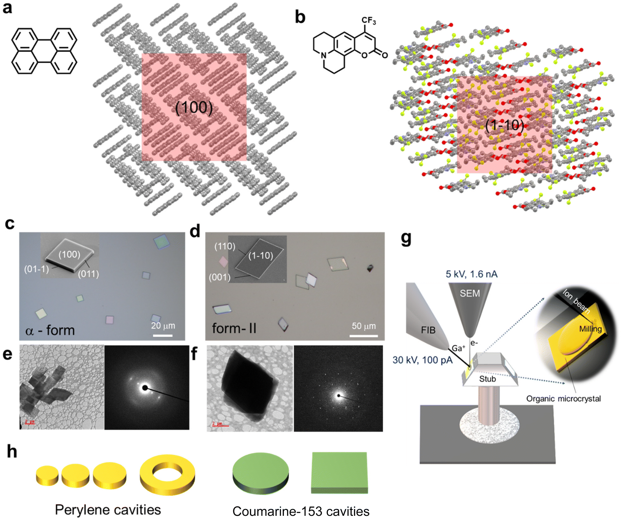 | ||
| Fig. 1 (a and b) Molecular structures of perylene and coumarin-153, respectively, along with their corresponding packing in the (100) and (1−10) planes. (c and d) Optical microscopy images of perylene (α form) and coumarin-153 (form-II), respectively. The insets show the field emission scanning electron microscopy (FESEM) images of the corresponding single crystals. (e and f) Transmission electron micrographs and selected area electron diffraction data of perylene and coumarin-153, respectively. (g) Schematic representation of focused ion beam milling of the microcrystal into a disc shape. (h) The sketches of FIB milled single crystal microcavities of various shapes and dimensions. | ||
Results and discussion
The single crystallinity of the prepared α-form perylene microcrystals9 was confirmed by the electron diffraction studies performed on a transmission electron microscope (Fig. 1e). To investigate the size-dependent optical cavity effect of microcavities of the same height but with different diameters, a i large perylene crystal (thickness ≈2.5 μm measured by AFM) was selected (Fig. 2a). Intentionally the selected single perylene crystal was broken into three pieces using an AFM cantilever tip force. The broken pieces are movable with an AFM cantilever tip. Therefore, after milling, the obtained resonators can also be moved and integrated with other optical modules. As the perylene crystals are not electrically conductive, a thin layer of gold was coated to facilitate simultaneous field emission scanning electron microscopy (FESEM) studies during milling and to minimize ion implantation on the milled (100) crystal surface. Three circular-shaped discs (namely, disc-A, disc-B, and disc-C) of diameters 3.88, 4.83, and 5.74 μm were milled using FIB on a shoe-shaped single perylene crystal (Fig. 2b).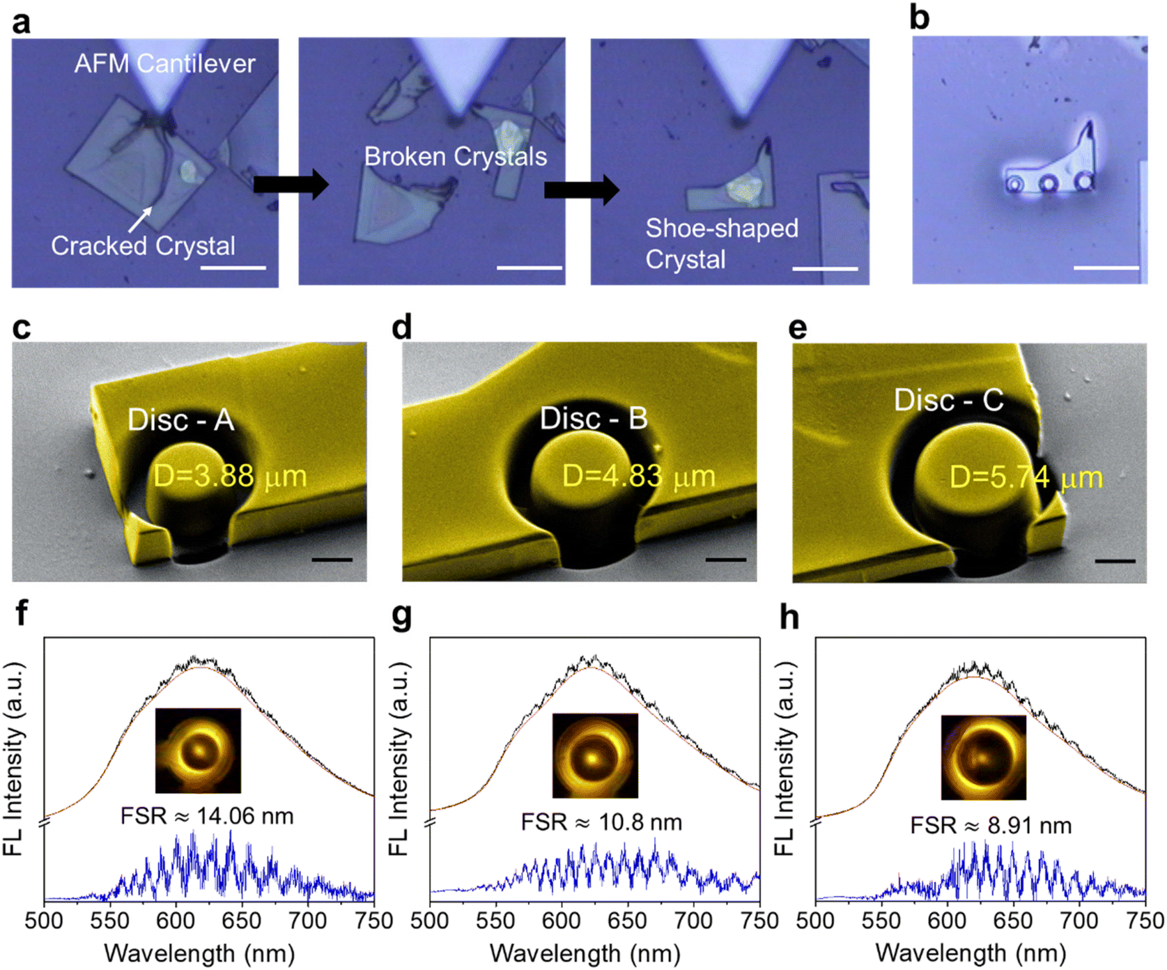 | ||
| Fig. 2 (a) A series of optical microscopy images showing the breaking of a rectangular-shaped perylene single crystal and its physical separation. (b) Optical image of three different discs made by FIB milling of a shoe-shaped crystal. (c–e) The color-coded FESEM images of the three fabricated microdiscs (disc-A to -C) of varying diameters. (f–h) The spectra showing the FL raw data (black), background-subtraction data (red) and the subtracted spectral data (optical resonances, blue) of three milled microdiscs. Insets show the corresponding FL images. Scale bars 30 μm (white) and 2 μm (black). | ||
The color-coded FESEM images show the fine finishing of the circular shape and smooth surface morphology of the fabricated microdiscs (Fig. 2c–e). Immediately after the fabrication of microdiscs, their optical properties were investigated on a confocal optical microscope setup in the transmission mode, by irradiating them (at the centre) with a 405 nm continuous wave diode laser (power 0.1 mW). At the point of excitation, yellow FL of perylene was observed without any sign of optical resonances. The FL spectrum recorded at the microdisc periphery (displaying ring-shaped bright emission) possessed periodic sharp peaks indicative of WGMs (Fig. S2†). However, the optical modes observed in disc-A to disc-C were not well pronounced due to the gold coating present on the surface of the discs (Fig. S2†). Therefore, the gold layer on the cover slip consisting of the fabricated microdiscs was removed by washing with Lugol's iodine solution. The spectra obtained at the periphery of the resultant discs (disc-A, disc-B, and disc-C) revealed an enhanced FL spectral intensity with clearly observable optical modes (Fig. 2f–h and Fig. S2†). The free spectral range (FSR, which refers to the distance between the two consecutive modes at a particular wavelength in the FL spectrum; FSR = λm − λm+1) of disc-A to disc-C was 14.06, 10.8, and 8.91 nm, respectively. This result shows that the cavity effect is preserved in microdiscs of varying diameters as supported by decreased FSR values with an increase in cavity diameter in accordance with the formula FSR ∝ 1/D (Fig. S2c†).
Attaining a ring-shaped microcrystal with specific dimensional requirements via crystal growth techniques like crystallization, self-assembly, sublimation, etc., is practically not possible. Hence, we selected a naturally-grown single perylene microcrystal (dimensions 8.4 × 8.17 μm2) to obtain a ring geometry of the desired size via FIB milling. Contact mode AFM exhibited the smooth surface of the microcrystal and the thickness is found to be 0.35 μm (Fig. S3†). Furthermore, photonic studies revealed that the selected microcrystal acts as a WGM cavity exhibiting an FSR of 3.18 nm (Fig. S3c–e†). The gold-coated crystal was milled into a ring-shaped geometry with outer and inner diameters of 6.3 μm and 2.35 μm, respectively (Fig. 3a and b). The sequential carving of the perylene microcrystal into a ring resonator using FIB milling is shown in Fig. S3b.† The color-coded FESEM and the optical microscopy images of the ring-shaped perylene crystal showed a smooth crystal surface morphology (Fig. 3a and b). After the removal of the gold coating (Fig. S4†), the ring resonator was excited with a 405 nm continuous wave laser and the FL spectrum was recorded at the outer convex periphery. The FL spectrum revealed relatively broad optical modes having an FSR of 20.75 nm, signifying the resonator characteristics (Fig. 3c and S3f–h†). The FDTD numerical calculations revealed that the electric field (|E|2, which is the square of the component of the circulating field normal to the disks’ surface) of the trapped light (for example: 570 nm optical mode) is predominantly confined at the outer periphery of the ring resonator (Fig. 3d). The ring resonator modes look like modes of disc resonators with the same diameter, as the inner diameter of the ring resonator is too small to influence the electric field distribution.
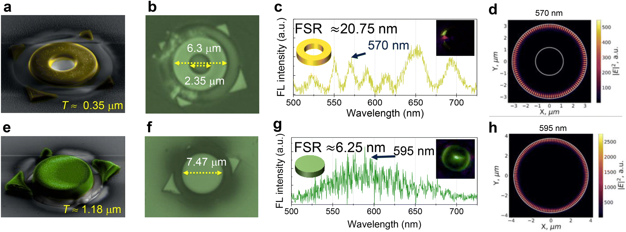 | ||
| Fig. 3 (a and e) The color-coded FESEM images, (b and f) optical microscopy images and (c and g) the corresponding FL background subtracted spectra of the fabricated perylene and coumarin-153 microresonators, respectively. The insets in (c) and (g) show the FL images during focused optical excitation. FDTD calculations displaying (d) |E|2 distribution for the 570 nm mode in the ring resonator and (h) 595 nm mode in the disc resonator. | ||
Furthermore, to generalize this technique, FIB milling along with microspectroscopic studies was carried out on coumarin-153 crystals. Here, the microcrystals of coumarin-153 were prepared using the ambient pressure vapor deposition technique (see the ESI† for details). The TEM studies on these microcrystals further confirmed their single crystalline nature (Fig. 1f). The microspectroscopic studies on coumarin-153 microcrystals (dimensions: 9.8 × 9.41 μm2) revealed a broad FL spectrum ranging from 475 to 725 nm, which corresponds to the polymorphic form-II.45 The major facets were found to be (1−10), (110) and (001) (inset of Fig. 1d). As per our plan, the selected coumarin-153 microcrystal was gold-coated and milling was performed orthogonal to the (1−10) facet to fabricate a microdisc of diameter 7.47 μm (Fig. 3e, f and S5†). The thickness of the crystal measured using AFM in the contact mode is found to be 1.18 μm (inset of Fig. S5d†). The series of steps involved during the FIB milling is shown in Fig. S5a and b.† The color-coded FESEM and optical microscopy images reveal geometrical perfection and smooth finishing of the disc-shaped crystal (Fig. 3e and f). Photonic studies revealed that the disc-shaped crystal acts as a microresonator by emitting resonance modes with an FSR of 6.25 nm, respectively (Fig. 3g and S5f–h†). As expected, the FDTD calculations confirm the distribution of light's electric field around the periphery of the microdisc cavity for the representative 595 nm mode (Fig. 3h).
Later, two more rhombus-shaped coumarin-153 microcrystals (crystal-1: 8.31 × 9.96 μm2; thickness ≈0.91 μm, and crystal-2: 10.98 × 9.02 μm2; thickness ≈1.33 μm) shown in Fig. S6c, d and S7a, b,† respectively, were selected. The photonic studies of crystal-1 and -2 showed a series of sharp optical modes in the FL spectra, confirming crystal's resonator characteristics before milling. The FSR values of the crystal resonators were found to be ≈4.07 nm, and ≈4.8 nm, respectively (Fig. S6e and S7c†). The resonator characteristics of these coumarin-153 crystals arise due to multiple reflections of FL by the light-reflective edges of the crystals. FESEM images of the gold-coated crystals before milling clearly show the two rough edges of the crystal damaged during AFM contact mode measurement (Fig. S6b†). On these crystals, FIB milling was done in such a way to fabricate rectangular (dimensions: 6.3 × 5.5 μm2, Fig. S6†) and circular disc (diameter ≈2.5 μm; height ≈1.33 μm, Fig. S7†) shaped microcavities (Fig. 4a, b, e and f). Interestingly, without the removal of the gold coating, photonic experiments on these two crystals revealed an intense FL spectrum along with optical modes with an FSR of 8.15 nm and 23.14, respectively (Fig. 4c and g).
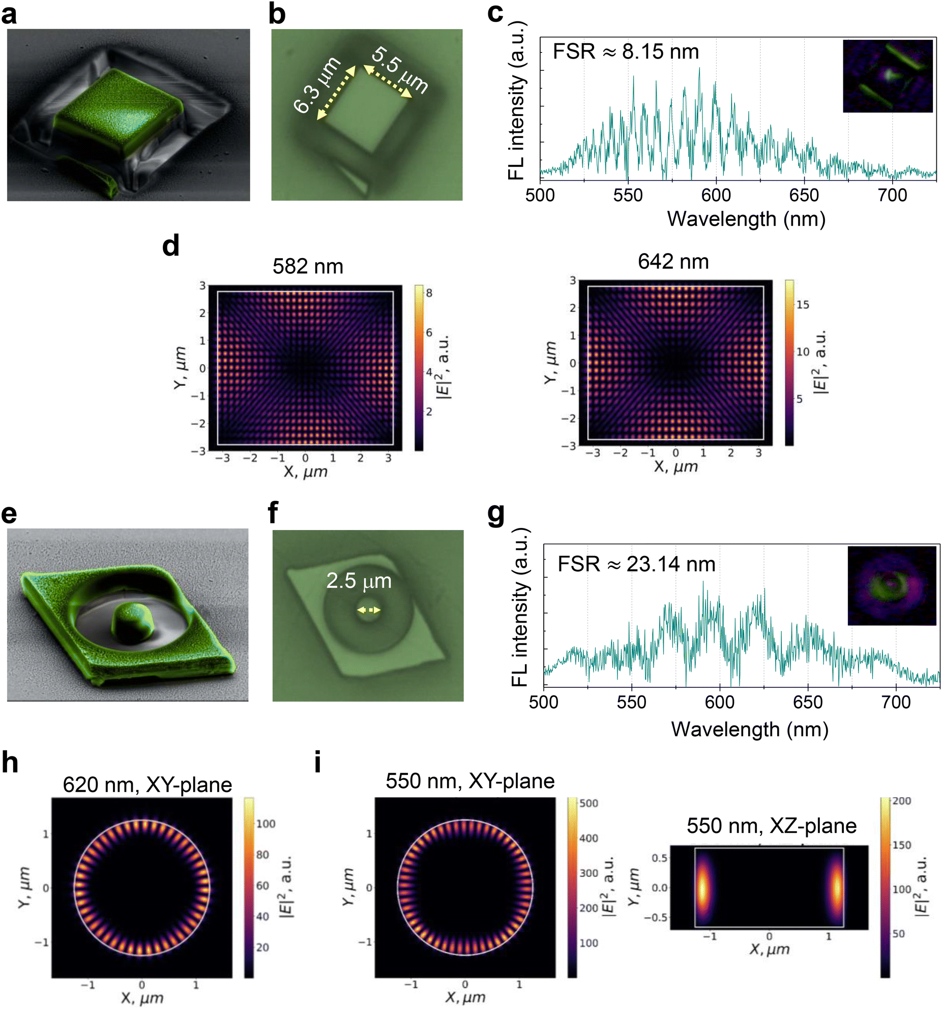 | ||
| Fig. 4 (a and e) Colored FESEM images, (b and f) optical microscopy images, and (c and g) the corresponding FL background-subtracted spectra of microrectangle and microdisc of coumarin-153, respectively. Insets in (c) and (g) show the corresponding FL image. FDTD calculations displaying |E|2 distribution for (d) 582 nm and 642 nm modes for the rectangular-shaped resonator and (h and i) 620 nm and 550 nm microdisc of coumarin-153. | ||
FDTD calculations were performed on both the fabricated rectangular and disc-shaped photonic cavities. The calculated electric field distribution for the wavelengths 582 nm and 642 nm in the rectangular microcrystal cavity is shown in Fig. 4d. Similarly, 2D and 3D FDTD calculations were performed for the disc cavity for 620, 550, 614 and 634 nm modes (Fig. 4h, i and Fig. S8†). As expected from the geometry, 2D FDTD shows the localization of an intense electric field around the circular periphery. The calculated azimuthal mode numbers for 620 nm and 550 nm peaks are 22 and 25, which suggests that the cavity acts as a WGM type. The 3D FDTD calculations revealed the WGM with higher-order field distribution in a plane perpendicular to the mode circulation direction (Fig. 4i).
Conclusions
In summary, FIB milling was performed to obtain organic photonic components, namely ring-, disc- and rectangular-resonators from single microcrystals of chemically different perylene and coumarin-153 molecules. The fabricated photonic components revealed different optical traits after milling. Perylene crystals required washing with gold etchants to reveal optical modes while the high quantum yield coumarin-153 crystals did not require any of this post-processing treatment. The perylene single crystals are mechanically movable before milling; however, after milling, the fabricated crystal resonators were attached to the substrate firmly due to milling-induced local heat. To minimize unwanted Ga ion implantation on the surface and amorphization, beam parameters were optimized to 30 kV and 100 pA. Higher ion energies reduce the milling time, but at the expense of amorphization, ion-implantation and more ion exposure to the milled areas, resulting in crystal's FL quenching. The use of lower ion energies (beam current: 50 pA and lower) increases the milling duration and the geometry of the milling area might be affected by crystal drifting, producing shapes with less geometrical precision. Particularly, in post-processing treatment, there should not be any chemical interaction between the etchant and the molecular single crystal. The FDTD numerical calculation revealed that light's electric field inside the crystal microcavities was localized at the periphery of the ring and disc resonators. For the rectangular resonator, the field is distributed nearly around the edges of the crystal. The obtained results validate the generality of the FIB milling technique to carve out optical components of precise shape and dimension from organic molecular single crystals. The field of crystal photonics foundry, i.e. FIB milling of organic crystals into photonic modules, has the potential to enable industrial-scale manufacturing of organic photonic circuits and devices.Author contributions
RC conceived the idea of the crystal photonics foundry project. VVP and MC carried out the experiments under the supervision of RC. EM carried out the FDTD numerical calculations. The paper was written through the contributions of all authors. All authors have approved the final version of the paper.Conflicts of interest
The authors declare no conflict of interest.Acknowledgements
RC, VVP and MC thank the advanced facility for microscopy and microanalysis of IISc Bangalore for allowing us to carry out FIB milling experiments. RC thanks the University of Hyderabad-Institution of Eminence Project (UoH-IoE-RC1-20-003), SERB-STAR (No. STR/2022/000011) and IISc-STARS, India for funding.References
- L. A. Coldren, S. W. Corzine and M. L. Mašanović, Diode Lasers and Photonic Integrated Circuits, 2012, DOI:10.1002/9781118148167.
- D. Thomson, A. Zilkie, J. E. Bowers, T. Komljenovic, G. T. Reed, L. Vivien, D. Marris-Morini, E. Cassan, L. Virot, J.-M. Fédéli, J.-M. Hartmann, J. H. Schmid, D.-X. Xu, F. Boeuf, P. O'Brien, G. Z. Mashanovich and M. Nedeljkovic, J. Opt., 2016, 18, 073003 CrossRef.
- W. Bogaerts, S. K. Selvaraja, P. Dumon, J. Brouckaert, K. De Vos, D. Van Thourhout and R. Baets, IEEE J. Sel. Top. Quantum Electron., 2010, 16, 33 CAS.
- W. Bogaerts, R. Baets, P. Dumon, V. Wiaux, S. Beckx, D. Taillaert, B. Luyssaert, J. Van Campenhout, P. Bienstman and D. Van Thourhout, J. Lightwave Technol., 2005, 23, 401 CAS.
- H. Rong, Y.-H. Kuo, A. Liu, M. Paniccia and O. Cohen, Opt. Express, 2006, 14, 1182 CrossRef PubMed.
- W. Bogaerts and L. Chrostowski, Laser Photonics Rev., 2018, 12, 1700237 CrossRef.
- K. Takazawa, J. I. Inoue, K. Mitsuishi and T. Takamasu, Phys. Rev. Lett., 2010, 105, 067401 CrossRef PubMed.
- W. Zhang, J. Yao and Y. S. Zhao, Acc. Chem. Res., 2016, 49, 1691 CrossRef CAS PubMed.
- V. V. Pradeep, N. Mitetelo, M. Annadhasan, M. Popov, E. Mamonov, T. Murzina and R. Chandrasekar, Adv. Opt. Mater., 2020, 8, 1901317 CrossRef CAS.
- Y. S. Zhao, A. Peng, H. Fu, Y. Ma and J. Yao, Adv. Mater., 2008, 20, 1661–1665 CrossRef CAS.
- R. Huang, C. Wang, Y. Wang and H. Zhang, Adv. Mater., 2018, 30, 1800814 CrossRef PubMed.
- Z. Yu, Y. Wu, L. Xiao, J. Chen, Q. Liao, J. Yao and H. Fu, J. Am. Chem. Soc., 2017, 139, 6376 CrossRef CAS PubMed.
- M. Godumala, A. V. Kumar and R. Chandrasekar, J. Mater. Chem. C, 2021, 9, 14115 RSC.
- N. Mitetelo, D. Venkatakrishnarao, J. Ravi, M. Popov, E. Mamonov, T. V. Murzina and R. Chandrasekar, Adv. Opt. Mater., 2019, 7, 1801775 CrossRef.
- J. Ravi, D. Venkatakrishnarao, C. Sahoo, S. R. G. Naraharisetty, N. Mitetelo, A. A. Ezhov, E. Mamonov, T. Murzina and R. Chandrasekar, Chem. Nanostruct. Mater., 2018, 4, 764 CAS.
- N. Mitetelo, J. Ravi, S. Mondal, U. Venkataramudu, E. Mamonov, M. Popov, A. Maydykovskiy, G. Vaitheeswaran, T. Murzina and R. Chandrasekar, Adv. Opt. Mater., 2022, 11, 2201635 CrossRef.
- S. Ghosh and C. M. Reddy, Angew. Chem., Int. Ed., 2012, 51, 10319 CrossRef CAS PubMed.
- S. Saha, M. K. Mishra, C. M. Reddy and G. R. Desiraju, Acc. Chem. Res., 2018, 51, 2957 CrossRef CAS PubMed.
- P. Naumov, S. Chizhik, M. K. Panda, N. K. Nath and E. Boldyreva, Chem. Rev., 2015, 115, 12440 CrossRef CAS PubMed.
- E. Ahmed, D. P. Karothu and P. Naumov, Angew Chem., Int. Ed., 2018, 57, 8837 CrossRef CAS PubMed.
- H. Liu, Z. Lu, Z. Zhang, Y. Wang and H. Zhang, Angew. Chem., Int. Ed., 2018, 57, 8448 CrossRef CAS PubMed.
- Q. Lv, M. Zheng, X.-D. Wang and L.-S. Liao, Small, 2020, 18, 2203961 CrossRef PubMed.
- Q. Lv, X.-D. Wang, Y. Yu, M.-P. Zhuo, M. Zheng and L.-S. Liao, Nat. Commun., 2022, 13, 3099 CrossRef CAS PubMed.
- Y. Ma, C.-F. Xu, X.-R. Mao, Y. Wu, J. Yang, L.-P. Xu, M.-P. Zhuo, H. Lin, S. Zhuo and X.-D. Wang, J. Am. Chem. Soc., 2023, 145, 9285–9291 CrossRef CAS PubMed.
- M.-P. Zhuo, J.-J. Wu, X.-D. Wang, Y.-C. Tao, Y. Yuan and L.-S. Liao, Nat. Commun., 2019, 10, 3839 CrossRef PubMed.
- M. Annadhasan, D. P. Karothu, R. Chinnasamy, L. Catalano, E. Ahmed, S. Ghosh, P. Naumov and R. Chandrasekar, Angew. Chem., Int. Ed., 2020, 59, 13821 CrossRef CAS PubMed.
- Z. Lu, Y. Zhang, H. Liu, K. Ye, W. Liu and H. Zhang, Angew. Chem., Int. Ed., 2020, 59, 4299 CrossRef CAS PubMed.
- J. M. Halabi, E. Ahmed, L. Catalano, D. P. Karothu, R. Rezgui and P. Naumov, J. Am. Chem. Soc., 2019, 141, 14966 CrossRef CAS PubMed.
- N. Chandrasekhar, M. A. Mohiddon and R. Chandrasekar, Adv. Opt. Mater., 2013, 1, 305 CrossRef.
- P. Hui and R. Chandrasekar, Adv. Mater., 2013, 25, 2963 CrossRef CAS PubMed.
- D. Venkatakrishnarao, Y. S. L. V. Narayana, M. A. Mohaiddon, E. A. Mamonov, N. Mitetelo, I. A. Kolmychek, A. I. Maydykovskiy, V. B. Novikov, T. V. Murzina and R. Chandrasekar, Adv. Mater., 2017, 29, 1605260 CrossRef PubMed.
- D. Venkatakrishnarao, E. A. Mamonov, T. V. Murzina and R. Chandrasekar, Adv. Opt. Mater., 2018, 6, 1800343 CrossRef.
- D. Venkatakrishnarao, M. A. Mohiddon, N. Chandrasekhar and R. Chandrasekar, Adv. Opt. Mater., 2015, 3, 1035 CrossRef CAS.
- J. Ravi, A. V. Kumar, D. P. Karothu, M. Annadhasan, P. Naumov and R. Chandrasekar, Adv. Funct. Mater., 2021, 31, 2105415 CrossRef CAS.
- J. Ravi and R. Chandrasekar, Adv. Opt. Mater., 2021, 9, 2100550 CrossRef CAS.
- R. Chandrasekar, Chem. Commun., 2022, 58, 3415 RSC.
- R. Chandrasekar, Small, 2021, 17, 2100277 CrossRef CAS PubMed.
- M. Annadhasan, A. R. Agrawal, S. Bhunia, V. V. Pradeep, S. S. Zade, C. M. Reddy and R. Chandrasekar, Angew. Chem., Int. Ed., 2020, 59, 13852 CrossRef CAS PubMed.
- M. Annadhasan, V. V. Pradeep, A. V. Kumar, J. Ravi and R. Chandrasekar, Small Struct., 2022, 3, 2100163 CrossRef CAS.
- J. Ravi, A. Vinod Kumar, M. Annadhasan and R. Chandrasekar, Adv. Opt. Mater., 2022, 10, 2102545 CrossRef CAS.
- A. V. Kumar, M. Godumala, J. Ravi and R. Chandrasekar, Angew. Chem., Int. Ed., 2022, 61, e202212382 CAS.
- A. V. Kumar, E. Mamonov, T. Murzina and R. Chandrasekar, Adv. Opt. Mater., 2022, 10, 2201507 Search PubMed.
- A. V. Kumar and R. Chandrasekar, Adv. Opt. Mater., 2022, 10, 2201009 Search PubMed.
- V. V. Pradeep and R. Chandrasekar, Adv. Opt. Mater., 2022, 10, 2201150 CrossRef CAS.
- U. Venkataramudu, M. Annadhasan, H. Maddali and R. Chandrasekar, J. Mater. Chem. C, 2017, 5, 7262 RSC.
Footnote |
| † Electronic supplementary information (ESI) available. See DOI: https://doi.org/10.1039/d3nr02229c |
| This journal is © The Royal Society of Chemistry 2023 |