
 Open Access Article
 This Open Access Article is licensed under a Creative Commons Attribution-Non Commercial 3.0 Unported Licence
Progress on the in situ imaging of growth dynamics of two-dimensional materials
Xiaokai
Zhu
 ab,
Honggang
Wang
abc,
Kangkang
Wang
ab and
Liming
Xie
*ab
ab,
Honggang
Wang
abc,
Kangkang
Wang
ab and
Liming
Xie
*ab
aCAS Key Laboratory of Standardization and Measurement for Nanotechnology, National Center for Nanoscience and Technology, Beijing 100190, P.R. China. E-mail: xielm@nanoctr.cn
bUniversity of Chinese Academy of Sciences, Beijing 100049, P.R. China
cDepartment of Chemistry, Tsinghua University, Beijing 100084, China
First published on 23rd June 2023
Abstract
One key issue to promote the industrialization of two-dimensional (2D) materials is to grow high-quality and large-scale 2D materials. Investigations of the growth mechanism and growth dynamics are of fundamental importance for the growth of 2D material, in which in situ imaging is highly needed. By applying different in situ imaging techniques, details for growth process, including nucleation and morphology evolution, can be obtained. This review summarizes the recent progress on the in situ imaging of 2D material growth, in which the growth rate, kink dynamics, domain coalescence, growth across the substrate steps, single-atom catalysis, and intermediates have been revealed.
 Xiaokai Zhu | Xiaokai Zhu obtained his B.Sc. in chemistry from Huazhong University of Science and Technology in 2017. Currently he is a Master student at National Center for Nanoscience and Technology. His research interest focuses on the synthesis of 2D materials as well as the understanding of their growth mechanisms. |
 Liming Xie | Dr Liming Xie is currently a professor at National Center for Nanoscience and Technology (NCNST, China). He received his Ph.D. degree from Peking University in 2009 and during which he went to MIT as a visiting student in 2007–2008. He did his postdoctoral research at Stanford University in 2009–2012 and joined NCNST as a professor in 2012. His research interest is on synthesis, Raman spectroscopy and devices of 2D materials. |
1. Introduction
The discovery of atomically thin graphene films by Novoselov et al. in 2004 has boosted the research on two-dimensional (2D) materials.1 So far, many branches of 2D materials have been identified including graphene,1 hexagonal boron nitride (h-BN), transition metal dichalcogenides (TMDs, such as MoS2,2 WTe2,3 WSe2,4 and ReS2![[thin space (1/6-em)]](https://www.rsc.org/images/entities/char_2009.gif) 5), black phosphorus (BP),6 transition metal halides,7 metal thio/selenophosphates,8 transition metal carbides and nitrides (MXenes)9,10 and so on.11–15 Due to their atomic thickness, dangling-bond free surfaces, and unique electronic structures, 2D materials have been endowed with novel physical properties such as massless fermions,16 Ising superconductivity,17 quantum Hall effect,18etc. As a result, extensive effort has been made to explore the fundamental science as well as the electronic applications of 2D materials.
5), black phosphorus (BP),6 transition metal halides,7 metal thio/selenophosphates,8 transition metal carbides and nitrides (MXenes)9,10 and so on.11–15 Due to their atomic thickness, dangling-bond free surfaces, and unique electronic structures, 2D materials have been endowed with novel physical properties such as massless fermions,16 Ising superconductivity,17 quantum Hall effect,18etc. As a result, extensive effort has been made to explore the fundamental science as well as the electronic applications of 2D materials.
Toward the fundamental research and potential device applications, it is highly demanded to synthesize 2D materials with high quality and high uniformity in a large area. Besides, the growth of 2D materials with precise layer numbers, low density of defects, and desired crystal orientations is more desirable. To date, 2D materials have been grown by physical vapour deposition (PVD),7 molecular beam epitaxy (MBE),19 atomic layer deposition (ALD),20 chemical vapour deposition (CVD),21,22 metal–organic CVD (MOCVD),23 and so on. To meet the requirements, a thorough understanding of the growth mechanisms and the precise measurement of the growth dynamic parameters are needed. So far, ex situ experiments and simulations have been implemented to gain information about the growth mechanisms and growth dynamics.24–29 However, ex situ experiments require to interrupt the growth process, which is time-consuming and also cannot exclude the growth or etching during the cooling down process. Alternatively, in situ imaging of the growth is more preferred to capture the chemical and physical process in real-time. The generally used in situ techniques are presented in Fig. 1, including transmission electron microscopy (TEM), scanning electron microscopy (SEM), scanning tunnelling microscopy (STM), optical microscopy, X-ray photoelectron spectroscopy (XPS), X-ray diffraction (XRD), X-ray reflectivity (XRR), spectroscopic ellipsometry, differential reflectance spectroscopy (DRS) and Raman spectroscopy. Growth dynamics covering nucleation event, domain coalescence, and so on can be directly imaged. Further information, such as kink dynamics, can also be evaluated by model analysis and data fitting. All the growth dynamics information is critical for finely controlling the growth of 2D materials.
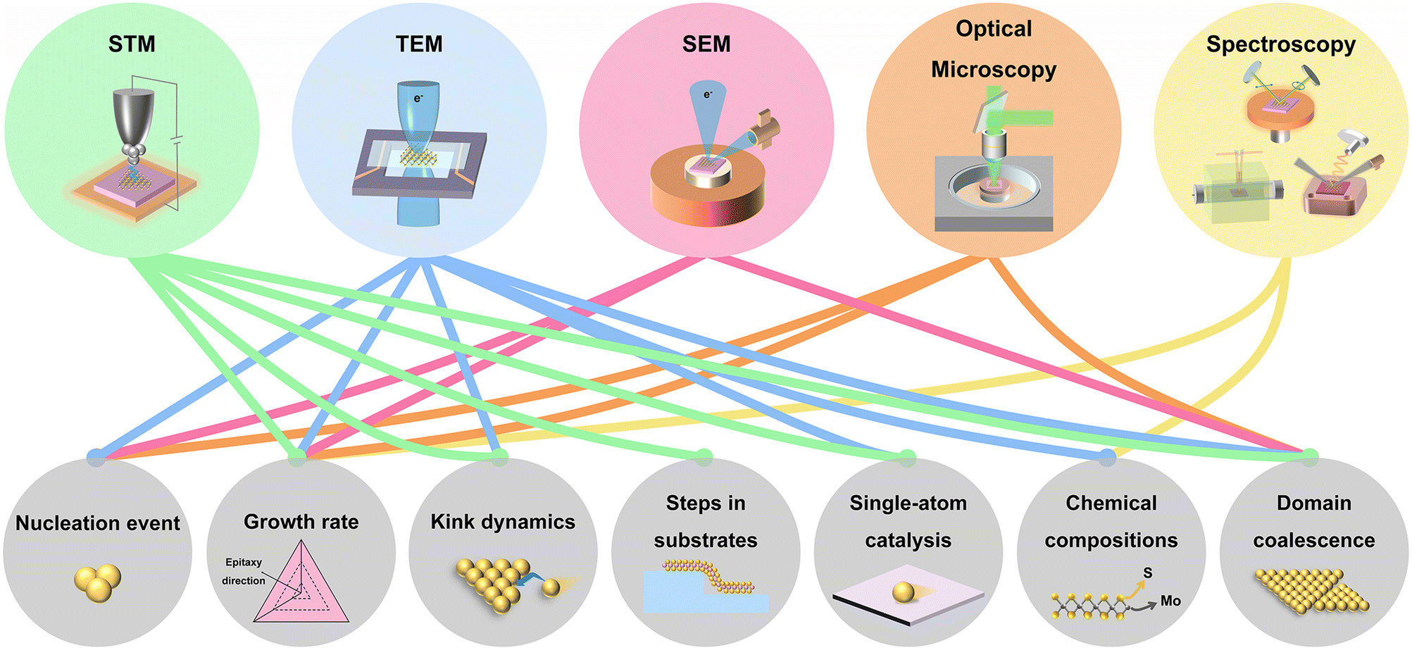 | ||
| Fig. 1 Schematic illustration of the used in situ techniques for 2D materials growth and the related research on the growth dynamics. | ||
However, there are difficulties in visualizing and imaging of the growth process. For example, the high temperature environment prevents a close imaging of the growth. Additionally, electron microscopic techniques require a vacuum condition. So, in most cases, a mini high-temperature stage/reactor is customized and put inside or under the characterization tools. In very few cases, the characterizations can also be directly used with the growth furnace/chamber, such as low energy electron microscopy (LEEM), DRS, and XPS. Using these in situ techniques, the nucleation events, evolution of crystal morphology/structures/chemical compositions during the material growth can be revealed.
In this review, we have summarized the recent progress on the in situ investigations of the growth dynamics of 2D materials. To begin with, the used techniques are briefly introduced. And then, the growth dynamics of 2D materials revealed by these in situ characterizations are discussed in detail, including growth rate, kink dynamics, domain coalescence, growth crossing the substrate steps, single-atom catalysis, and intermediates. At last, further research and challenges in the in situ imaging are discussed.
2. Characterization techniques used for in situ investigation
2.1. Imaging techniques
TEM offers atomic-scale insight into the nucleation, kink advancement, defect formation, atom diffusion, evolution of grain boundaries, and so on. To achieve in situ TEM imaging, a specially designed specimen holder is required.30 In most cases, in situ heating for TEM are realized by placing a heating element at the end of the specimen holder and using precise Joule heating and temperature dissipation to obtain precise and stable specimen temperatures.31 In 2005, Zhang et al. designed a micro electro-mechanical system (MEMS) device as a heater and a specimen carrier to observe the melt of bismuth nanoparticles.32 A thin film fabricated on the MEMS heater is used for heating by applying electric current.33 This thin film is usually made of metal, ceramic, or doped polysilicon. Very recently in 2023, Zhao et al. designed a sample holder with a 2D graphene based microheater, which can heat up the stage rapidly with less energy, and low thermal expansion at higher temperatures.34 Moreover, by integrating a microfabricated gas cell together with the MEMS heater, in situ characterizations in reactive gaseous and elevated temperature environment are both allowed. Nowadays, in situ studies are majorly conducted on such multi-functional reactors.33,35,36SEM utilizes a focused electron beam to scan over samples. The incident electrons generate secondary electrons (SE) and backscattered electrons (BSE) which carry rich information about the surface morphology and chemistry compositions of the sample. Similar to in situ TEM imaging, a specimen stage is designed for in situ SEM imaging. So far, numerous strategies have been implemented to heat the in situ stages, such as laser heating,37 current heating,38 and metallic coil heating.39 However, at the growth temperature, the thermal electrons emission from the heating element may induce interference to the in situ imaging.40 To reduce the thermal electrons, methods such as changing the composition for the specimen holder,41 encapsulation of the heating wires, and adjusting an electron filter systems are used.42In situ SEM has been applied to investigate the growth behaviours of graphene on different polycrystalline metal substrates. By collecting secondary electron signal, graphene with different layers could be discriminated from the different contrasts.43–47
To implement STM imaging, an atomically sharp tip is taken close to a conductive surface. Collecting the feedback of tunnelling current, atomic-resolution surface structure can be obtained. In real time characterization of growth process, thermal drift of the tip becomes severe. Hoogeman et al. designed a thermal-drift compensated piezoelectric scanner with a customized sample holder and then the thermal drift could be drastically reduced.48 Additionally, the scan speed has also been improved by increasing the mechanical resonances frequencies and the bandwidth of the feedback electronic components.49–51 In recent years, the behaviour of the atoms catalysis, the structure of crystal or edges, and different growth modes have been unveiled precisely by in situ STM imaging.51–56
With a sub-μm resolution and a large imaging field, optical microscopy is applied to recognize the nucleation sites, identify the layer number, visualize the growth process and domain coalescence, and track the morphology evolution, which can provide indispensable information for the growth dynamics. Compared with other techniques, optical microscopy can be operated under non-vacuum conditions and in a non-destructive way.57 Usually, a mini CVD chamber with a transparent optical window is needed for in situ optical imaging. In 2013, Puretzky et al. achieved real-time optical imaging of the growth of graphene on Ni substrate.58 And then in 2015, a radiation-mode optical microscopy was developed for imaging the growth of graphene on Cu substrate.59 Rasouli et al. designed a small-sized CVD chamber which could be put under a microscope lens to realize real-time observation. With this system, vapour–solid–solid growth and vapour–liquid–solid growth of 2D TMDs were observed.60
2.2. Spectroscopic techniques
Raman spectroscopy is a powerful and convenient tool to characterize material structures, chemical compositions, and so on. Usually, in situ Raman spectroscopy is a complementary tool with in situ optical microscopy. Thus, to conduct in situ characterizations, design of the reaction chamber is the same with in situ optical microscopy.58,61,62 However, at high temperatures, Raman signal becomes weaker and the thermal-emission background gets stronger. Usually, a short wavelength excitation is used to reduce the background interference. With Raman spectroscopy, layer number, compositions of intermediates, and final materials can be revealed.63,64X-ray characterization can identify crystal structures (by XRD), analyse surface elemental information (by XPS), and measure the electron density profile of materials and thickness of the film (by XRR). A small reactor is put in the equipment to conduct in situ characterizations. Recently, in situ XPS and XRD have been used to follow dynamic process such as the growth of MoS2,65 graphene,62,66 and 2D boroxine framework.67 As for in situ XRR, Jankowski et al. used this method to study the growth of graphene on molten Cu foil62,68 In 2020, Saedi et al. designed a CVD reactor which was integrated with an in situ optical microscopy, Raman, XRD, and XRR for real time investigations.66
Spectroscopic ellipsometry and DRS are remote and non-destructive analysis techniques. Spectroscopic ellipsometry can measure the compositions, film thickness, and growth rate and DRS can measure the compositions, growth rate, and electron state. Both spectroscopic techniques can be carried out under atmospheric pressure. So, a small CVD reactor is usually needed for in situ spectroscopic ellipsometry and DRS characterizations. Losurdo et al. applied in situ spectroscopic ellipsometry to clarify the effects of cleaning and annealing of metal substrate and carbon coverage at the surface on the growth behaviours. By controlling this process, precise graphene thickness was achieved.69In situ DRS can be applied in a real CVD reaction. Recently, Wang et al. built an in situ DRS system to monitor the growth process in a CVD furnace. A quartz window was designed on the top of the furnace which allowed the incident light beam to enter into the furnace.70
3. In situ investigation of 2D material growth
3.1. Imaging of the growth rate
The most straightforward information obtained via in situ techniques is the growth rate and its dependence on the temperature, gas flow rate, precursor, substrate, and so on.47,59–61,71–78 In 2015, the growth and etching of graphene on Cu substrate were observed by the radiation-mode optical microscopy (Rad-OM). Bright patches of graphene grains were clearly recognized (Fig. 2a). Typical time evolution of representative grain area at 985 °C was plotted in Fig. 2c in blue. Accurate graphene growth rates with different gas flow rates and different growth temperatures were extracted. For example, by increasing CH4 flow rates from 6 to 10 sccm, growth rates were first accelerated and then saturated. From the temperature dependence of growth rates, the activation energy was obtained, which suggested that the incorporation of precursor to graphene was the rate-determining reaction in the growth.59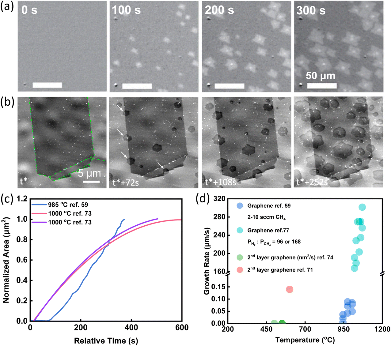 | ||
| Fig. 2 Schematic illustration of in situ imaging the growth rate of graphene. (a) Time-series SEM images of graphene growth with the CH4 flow rate of 5 sccm at 985 °C. Reproduced from ref. 59 with permission from Springer Nature, copyright 2015. (b) Time-series SEM images of graphene growth with C2H4 flow rate of 0.1 sccm at 1000 °C. White arrows highlight nucleation events at grain boundaries. t* corresponds to the induction period from C2H4 dosing until the first nucleation event was detected. Reproduced from ref. 73 with permission from American Chemical Society, copyright 2015. (c) A summary of the growth pattern of graphene showing the increase of the graphene areas with time from different research works. (d) A summary of growth rates of graphene obtained under various conditions from different research work. | ||
In situ SEM has also been used to evaluate the growth rates of graphene. The entire CVD process was observed via in situ SEM imaging. The growth was divided into three stages. Formation of new flakes was captured by in situ SEM (Fig. 2b) and growth rates were quantified based on in situ SEM data (Fig. 2c). During the first attachment-limited growth stage, the radial growth of graphene sheets was roughly constant. With the consumption of locally supersaturated precursor, a depletion zone appeared at the growth front leading to the second surface-diffusion-limited growth stage. When the growth fronts of neighbouring graphene approached to an approximate 3 μm interval, growth evolved to the third stage and the growth rates declined rapidly.73
In situ spectroscopy was also used to get a rough growth rate for graphene. Tsakonas et al. applied in situ DRS to plot the values of differential reflectance ΔR/R0 as a function of time. From the graph, the growth rates were finally quantified, indicated by cyan circles in Fig. 2d.77
Except for graphene, the growth dynamics of 2D van der Waals CdI2 and PbI2 on WS2, MoS2 and WSe2 was investigated. A custom-made system was used for in situ observation and Raman characterization of heterostructures growth dynamics. Sapphire with pre-grown WS2, MoS2 and WSe2 was used as substrates for the growth of CdI2 and PbI2. Two growth behaviours were observed depending on the temperature of substrate. At 285 °C, CdI2 nucleated on the WS2 flake. After 30 s growth, the nucleus grew and evolved into a hexagonal shaped crystal. When the edge of CdI2 reached the edge of WS2, the growth stopped (Fig. 3a). The time evolution of the domains showed a growth rate of 0.41 μm s−1. By decreasing the temperature to 260 °C, CdI2 grew with a suborbicular shape with no clearly defined facets (Fig. 3b). The size of CdI2 domains increased with time in a sublinear fashion and the growth rate slowed down as domain size increased. Based on the in situ images, their different growth patterns and rates have been concluded in Fig. 3c. The different growth behaviours at different temperatures were originated from the temperature-dependent surface diffusion and edge adsorption effects.76
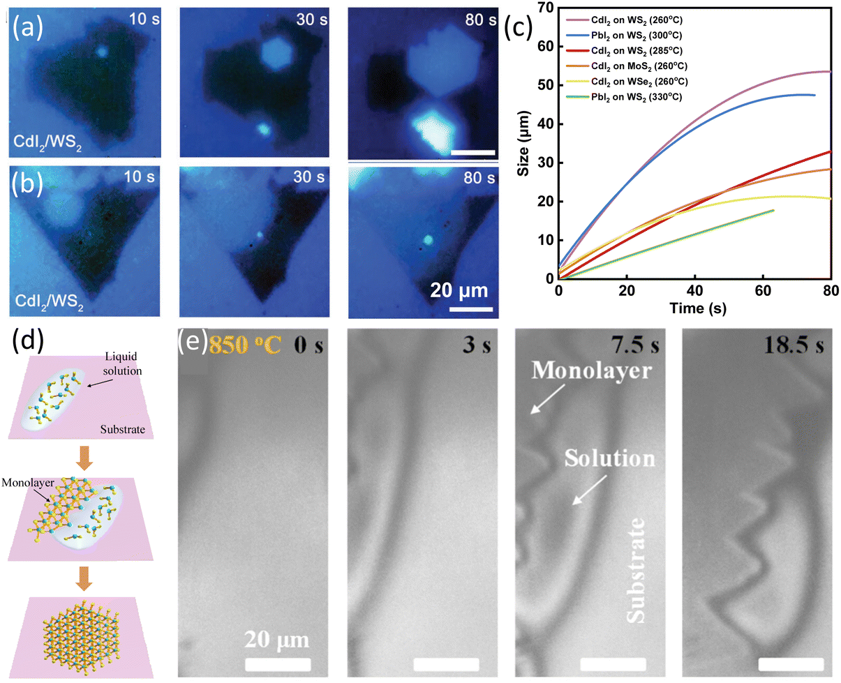 | ||
| Fig. 3 Schematic illustration of in situ imaging the growth rate of MI2 (M = Cd, Pb) and MoS2. (a) In situ real-time images of the growth process of CdI2/WS2 heterostructure at a growth temperature of 285 °C. (b) In situ real-time images of the growth process of CdI2/WS2 heterostructure at a growth temperature of 260 °C. (c) Plotting of the size of MI2 (M = Cd, Pb) with time at different temperatures. Reproduced from ref. 76 with permission from Wiley, copyright 2021. (d) Illustration of the LPEE process of TMDs. (e) In situ imaging of LPEE of MoS2 monolayers from the CsCl solution at 850 °C. Reproduced from ref. 78 with permission from American Chemical Society, copyright 2023. | ||
Very recently, our group applied a high-temperature optical microscope equipped into the CVD furnace79 to record the in situ growth process and developed a new liquid phase edge epitaxy method (LPEE) in Fig. 3d. In this new growth method, MoS2 contacted the liquid only at the edges and the growth was confined only along the MoS2 edges, resulting in precise-monolayer epitaxy of TMDs. Moreover, with the evolution of the flakes, the size of the liquid droplet decreased simultaneously, thus, indicating that the evaporation of the solvent was the driving force. The epitaxy rate was measured to be 1–2 μm s−1.78
3.2. Imaging of the kink dynamics
Based on the classic terrace-step-kink (TSK) model, the growth process includes adatom diffusion, nucleation and dynamics of the stable nucleus, atom attachment to create kinks, and kinks propagations along the edge. In particular, kinks are the most important and active sites for adding or removing atoms.24 Under a low supersaturation condition, kink generation can be the rate-limiting process.To elucidate how kinks form and how kinks advance, in situ STM was used to record the growth of h-BN (Fig. 4b and c). At the beginning, the shape of h-BN was a hexagon with three short edges and three long edges corresponding to a high energy and a low energy edge. The edges with higher energy disappeared quickly, forming a truncated triangular (Fig. 4b). In situ STM revealed that different kink creation rate contributed to the disappearance of the edges. New nanomesh units formed at kink sites and then moved along the edges. Kinks advanced along both edges at an equal speed.80
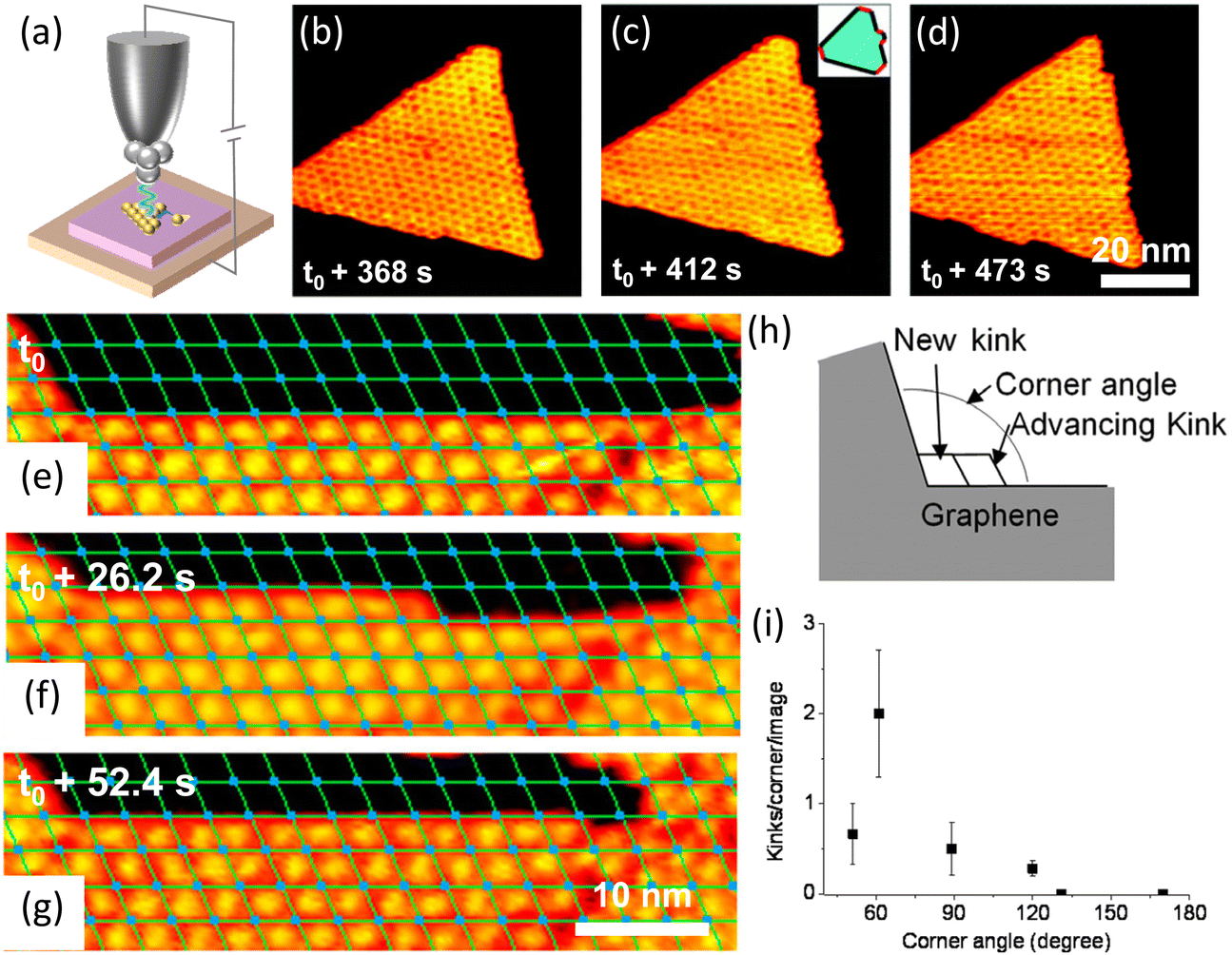 | ||
| Fig. 4 Schematic illustration of in situ imaging of kink dynamics at the edge during the growth of h-BN and graphene. (a) Diagram of an in situ scanning tunnelling microscope. (b–d) Sequential STM images of h-BN growth on Rh(111) with borazine precursor at 978 K. Reproduced from ref. 80 with permission from the American Physical Society, copyright 2010. (e–g) Sequential STM images for graphene growth at 975 K on Rh(111) with an ethylene pressure of 5.7 × 10⁻⁹ mbar. (h) Sketch of kink creation at a concave graphene corner and subsequent kink advancement. (i) Measured average number of kink creation events per STM image as a function of the angle of the concave graphene corner. Reproduced from ref. 52 with permission from American Chemical Society, copyright 2013. | ||
In 2013, Dong et al. imaged the kink dynamics in the growth of graphene on Rh(111). The growth started from creation of kinks and then the kinks advanced along the edge in units of the moiré pattern which consisted of 288 carbon atoms. And this observation was quite similar with the previous work on the growth of h-BN.
Kink advancement and kink creation at concave conners were also investigated. Kink creation rate at the concave conner depended on the corner angle (Fig. 4h and i). The kinks were created faster at the 60° concave corner and slower at the concave corners with angles larger than 120°.52
Wang et al. studied the kink-accelerated growth during the domain coalescence of graphene via in situ SEM characterizations. When two zigzag edges domains met, a concave corner with an angle of 120° formed. Then, fast attachment of growth species at the concave corner led to the formation of a new growth front (Fig. 5c–f). The edge of the new front was tilted 19.1° with respect to the initial zigzag edge, indicated in Fig. 5g. This edge had the highest possible kink density which was coincided with the theoretical simulations by Ma et al.24 Thus, this edge became the fastest growing edge during attachment-limited growth. Simulations of growth process at this concave angle presented in Fig. 5g was in accordance with the observation.81
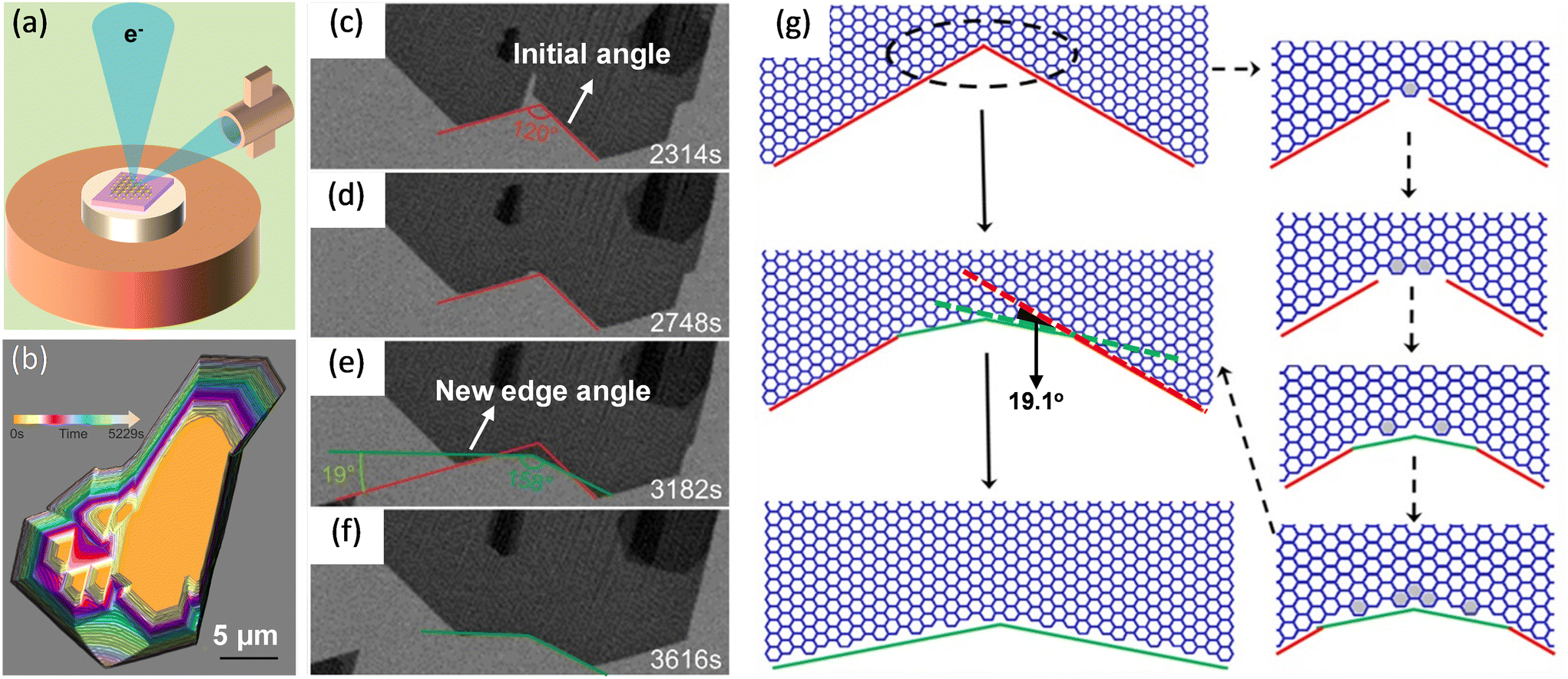 | ||
| Fig. 5 Schematic illustration of in situ imaging of kink dynamics at the concave corner during the growth of graphene. (a) Diagram of an in situ scanning electron microscope. (b) Shape evolution of the graphene domains during coalescence. (c–f) Sequential images showing the appearance of new edges at the concave corner during the coalescence. The new growth fronts which were tilted with a 19.1° dip angle. (g) Atomistic model of the growth process of a concave corner with an angle of 120° and zigzag edges in the case of well-aligned graphene domains. Reproduced from ref. 81 with permission from American Chemical Society, copyright 2020. | ||
These in situ investigations have revealed the important role for the kinks. During the growth, the creation of kinks determines the growth rate. Besides, when two domains coalesce, the shape of the final flake is affected by kinks. More in situ studies are needed to quantify the exact relationship between the kink concentrations and growth rates.
3.3. Imaging of the domain coalescence
One of the most possible strategies to obtain wafer scale single crystals of 2D materials is the seamless coalescence of small single-crystalline domains.82–85 After coalescence, there may be grain boundaries which play an important role in the device performance.86 The domain coalescence process has been observed by in situ STM,80,87 TEM,88,89 SEM,81 and optical microscopy.62 Liu et al. monitored the coalescence of graphene on Cu by in situ TEM. As the two grain boundaries with different crystallographic orientations moved closer, their grain edges contacted quickly but remained their original orientations. Hence, a clear grain boundary was formed.However, after 0.5 s, two grains reoriented and completely merged together. The grain boundary disappeared, resulting in a single grain with the same crystallographic orientation. This fast merge-reorientation phenomenon is explained by the first-order phase transition of the local atoms. In situ imaging also showed that the defects for the as-grown graphene could be repaired during growth.89
Jankowski et al. used in situ Rad-OM to monitor the growth behaviour of graphene on liquid copper at 1370 K. The whole growth process was demonstrated in Fig. 6a–d. During the growth, the flakes grew larger and flew close to each other, indicating the presence of an attractive long-range interaction between the domains. However, when the domains moved closer to each other (20–40 μm), there appeared a short-range repulsive interaction between them which kept the grains evenly distributed on the liquid copper. As the growth further proceeded, continuous and domain-boundary-free graphene film was formed eventually.62
 | ||
| Fig. 6 Schematic illustration of in situ imaging of domain coalescence processes during graphene growth and MoS2 growth. (a–d) In situ optical imaging of graphene growth on liquid copper. Reproduced from ref. 62 with permission from American Chemical Society, copyright 2021. (e–h) TEM images showing coalescence of MoS2 grains. Grains indicated by white and red arrows move toward the grain indicated by cyan arrow. Reproduced from ref. 88 with permission from Wiley, copyright 2019. | ||
These findings have elucidated the effect of substrates during the coalescence of graphene. Seamless graphene films were obtained both on Cu films and on liquid copper via different mechanisms. For TMDs, the investigation in the domain coalescence is far more limited.
Sang et al. observed the oriented attachment of nanograins during the growth of 2D MoS2via thermolysis of (NH4)2MoS4. The nanograins were initially formed at 600 °C. As shown in Fig. 6e–h, the middle grain slowly moved toward the left grain. After the middle grain attaching to the left grain, the middle grain reoriented to align with the left grain to reduce the total energy. In contrast, the right grain moved toward the middle grain but kept its orientation after attaching to the middle grain due to its larger size and hence a higher energy barrier for reorientation.88
3.4. Imaging of crossing over the substrate steps
Recently, the step-edge-guided method has shed light on the large-scale growth of single crystal 2D materials. Atomic steps on the vicinal surface of the substrate guide a unidirectional domain growth. Domains with the same orientations finally merge into a single crystalline thin film. Consequently, the understanding of how substrates and steps affect the growth process is needed.In 2011, Günther et al. observed a downhill growth mode for graphene using in situ STM. The collected data demonstrated that graphene preferentially grew across the descending steps with a carpet-mode.90 However, the graphene grown on the lower terrace was from the pointlike seeds at the step edge. These seeds led to different orientations of the graphene. At a low pressure and a high temperature, the Ru terraces moved with the front of graphene edges, and hence the graphene did not grow downhill across the atomic steps. Instead, this yielded large-size terraces and perfectly crystalline graphene films.91
Uphill and downhill growth modes were both observed by in situ STM imaging under different growth conditions for the growth of h-BN on Pd(111) surface (Fig. 7a and b). At a low temperature, due to a lower effective activation barrier at step sites, the nucleation and growth of h-BN occurred majorly at the ascending steps in spite of large terrace areas. The growth obeyed an uphill growth mode. Differently, at a high temperature and a low pressure, the deposition rate at terrace sites increased exceeding the deposition rate at step edges. Hence, the growth occurred on terraces. Since the growth at the descending Pd steps was kinetically suppressed, h-BN islands formed on terraces eventually followed a downhill growth mode.56
 | ||
| Fig. 7 Schematic illustration of in situ imaging of the h-BN growth across the substrate steps. (a and b) Representative in situ STM images acquire during the CVD growth of h-BN on Pd(111) at (a) temperature T = 573 K, borazine pressure p = 10–6 mbar and (b) T = 673 K, p = 10−7 mbar. Deposition times t indicated in the image panels are with respect to an arbitrary time during annealing the sample at the set T in UHV, at which borazine is introduced into the STM system. (c) Schematic of the h-BN growth modes at different deposition conditions. Different colours correspond to different rotational domains of h-BN. Reproduced from ref. 56 with permission from American Chemical Society, copyright 2020. | ||
Overall, these studies have suggested that the growth across steps relied on the substrates, the growth temperature, precursor pressure, and so on.
3.5. Imaging of single-atom catalysis
Single-atom catalysts have compelling potentials because each atom is accessible for the catalytic reaction with 100% atomic efficiency. Many studies have evidenced that single atoms will participate in the growth of graphene on metal substrates.92 The catalysis involves the connection of single atoms to the edge of 2D materials. And then, the growth (i.e., atom attachment) is catalysed at the catalysis site.In 2014, Liu et al. applied atomic resolution aberration-corrected STEM to investigate the graphene growth and domain boundary formation under electron-beam irradiation. During the second layer graphene growth, single Si atoms as catalyst were observed unexpectedly. A series of annular dark-field (ADF) images were captured by in situ TEM at 500 °C (Fig. 8a–d). On the left side of the dashed magenta line was the initial second layer of the graphene. A tip-growth mechanism could be observed, in which graphene grew next to Si atoms and Si atoms were pushed to the edge front.74
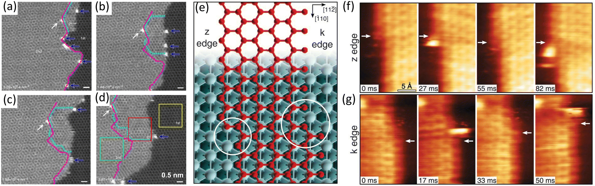 | ||
| Fig. 8 Schematic illustration of in situ imaging of the single-atom catalysis during graphene growth. (a–d) Sequential ADF images showing graphene from the step-edge of the bilayer graphene. The initial 2nd-layer step-edge is indicated by dashed magenta line, while the rotated 2+-layer highlighted by cyan dot line shows different moiré patterns and increases over time. Reproduced from ref. 74 with permission from Springer Nature, copyright 2014. (e–g) Sequential STM images during graphene growth along z and k edges. (e) Zigzag (z) and Klein (k) edges of a top-fcc epitaxial graphene layer on Ni(111). At both edges, the kink structures are highlighted by circles. (f) High-speed STM sequence acquired at 710 K in quasi-constant height mode at the z edge. White arrows indicate the position of C atoms in fcc-hollow sites near the kink. (g) Same as in (f) but for the k edge. Reproduced from ref. 54 with permission from American Association for the Advancement of Science, copyright 2018. | ||
Single Si atoms were also observed to catalyse the dissociation of carbon atoms from graphene in an aberration-corrected HRTEM.93 Several more research has been published to further reveal the mechanisms of single Fe,94 Cr,95 and Sn96 atom catalysis on the edge of graphene using in situ TEM imaging.
In 2018, Patera et al. directly visualized the growth of graphene on Ni(111) and uncovered how single Ni atoms involved in growth process at kink sites of graphene. At first glance of in situ STM images shown in Fig. 8f and g, carbon atoms started to incorporate at the kink sites and then propagated along the edge at both the z edge and the k edge. The presence of bright objects at the kink sites, which were Ni atoms, was also recorded in the images. As the Ni adatoms reached the kinks, a carbon dimer was formed nearby (Fig. 8f and g). This observation indicated that the addition of carbon atoms at kink sites was catalysed by single Ni atoms. Combining with DFT simulations, such a high catalysis activity was ascribed to a 35% decline of the rate-limiting energy barrier of the growth process with the Ni atoms.54
3.6. Imaging of the intermediates
Characterizations of the intermediate species during the growth is important to understand the growth pathway.Weatherup et al. uncovered how C2H2 was catalysed to form graphene on catalysts substrate based on in situ X-ray characterizations. Four intermediate steps were observed. Shortly after the introduction of C2H2 precursor, carbon decomposed from C2H2 bound to the high reactivity Ni surface sites (CA). And then, this surface carbon diffused into the Ni subsurface forming a Ni–C solid solution (CDis). Later, graphene (CGr) and defects (CB) emerged at the same time. Thus, a reduction of CB peak meant a reduction of defects, amorphous carbon, and domain boundary density.97,98
Combining in situ spectroscopy with in situ microscopy, the growth mechanism can be further revealed. In 2020, Xue et al. developed a versatile in situ system to investigate the sulfurization of MoO3. The system was equipped with an in situ optical microscope and a confocal Raman spectrometer. At 550 °C, the Raman peaks E2g and A1g of MoS2 were observed (Fig. 9a). Besides, peaks belonging to the intermediates of MoO2 or MoOS2 were also detected at initial stage (Fig. 9b). Additionally, in situ optical imaging revealed two growth modes. One mode was MoS2 monolayer grown around a solid nucleation site (Fig. 9c and d) and another mode was MoS2 grown from a liquid droplet (Fig. 9e and f). The first mode grew much faster and larger because of high density of intermediate MoO3−x vapours near the substrate surface, providing sufficient Mo for growth.61
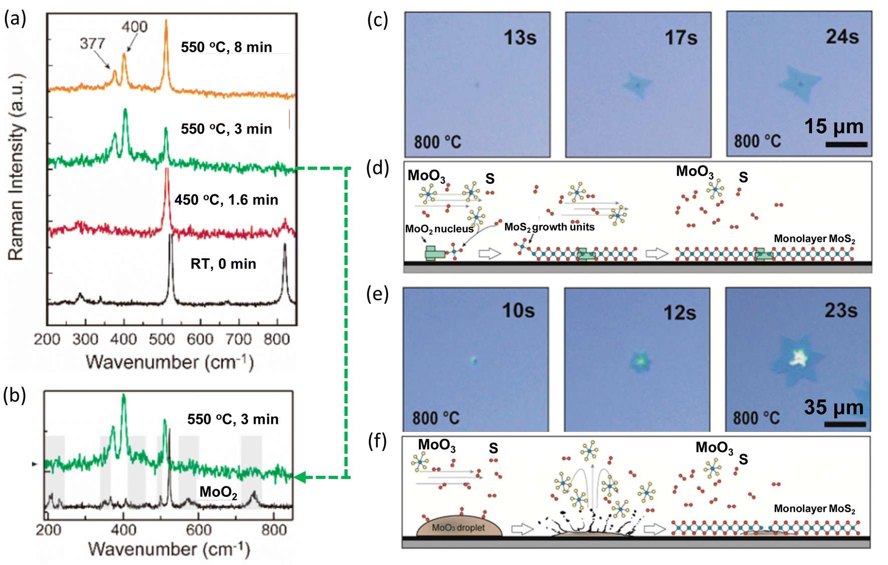 | ||
| Fig. 9 Schematic illustration of in situ imaging of the intermediates during MoS2 growth. (a) Raman spectra of MoO3 with S vapours at different temperatures. (b) Raman spectrum of MoO3 2D flakes sulfurized at 550 °C for 3 min and Raman spectrum of MoO2 at room temperature. (c) Growth mode of MoS2 monolayer growth around a nucleation site. (d) Schematic for MoS2 monolayer grown around a MoS2 nucleation site, in which the growth is fed by the vapour-state Mo sources. (e) Growth mode of MoS2 monolayer growth from MoO3 droplets. (f) Schematic for MoS2 monolayer from a MoO3 droplet, in which the growth is fed by the liquid droplet. Reproduced from ref. 61 with permission from American Chemical Society, copyright 2020. | ||
4. Conclusions
In this review, we have introduced in situ techniques used for visualizing the growth of 2D materials, including imaging techniques (such as TEM, STM, SEM, and optical microscopy) and spectroscopic techniques (such as DRS, spectroscopic ellipsometry, XRD, XRR, XPS and Raman). To realize precise heating and clearly imaging simultaneously inside or under in situ techniques, the sample holder or heating stage should be specially designed. As shown in Fig. 10, these in situ techniques can track the growth process at different spatial resolutions and different temporal resolutions.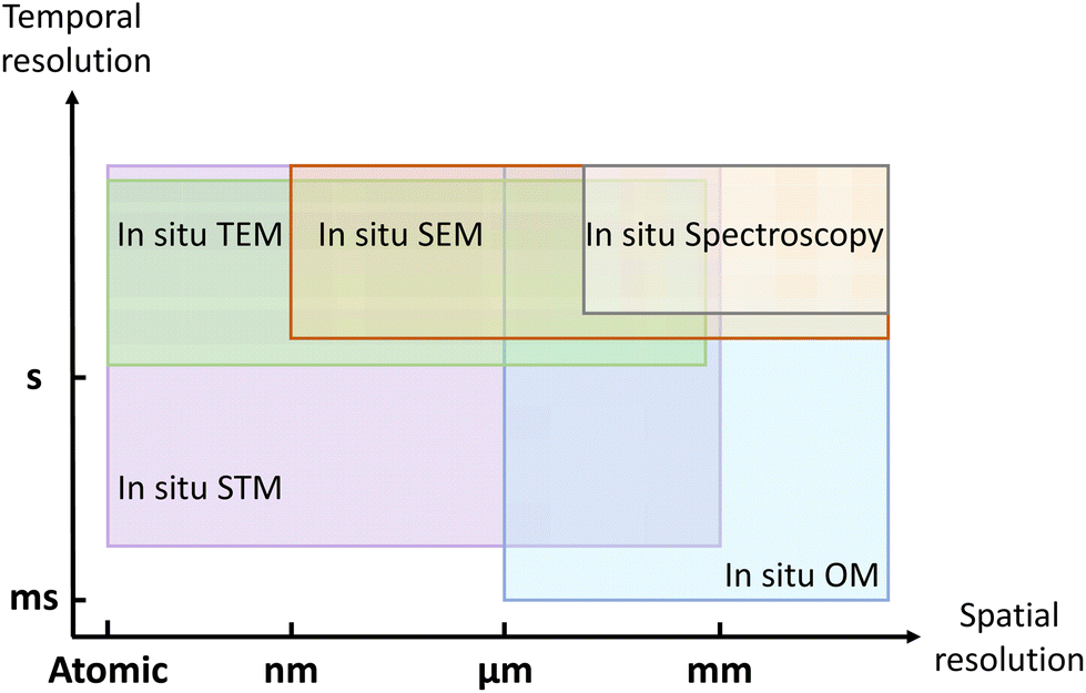 | ||
| Fig. 10 Schematic illustration of the spatial resolution and temporal resolution for in situ techniques. | ||
To evaluate how fast the 2D materials grow and how the morphology evolves, in situ optical microscope and in situ SEM can be the most suitable choices. In situ TEM can be applied to investigate the nucleation stage due to its atomic resolution. With the sensitivity to the surface, in situ STM can be used to visualize how 2D materials grow on the vicinal surface. In situ spectroscopy provides complementary information about the chemical compositions, surface information, and crystal structures. Utilizing these in situ techniques, the dynamic process of nucleation, edge epitaxy, single-atom catalysis, and substrate effect can be thoroughly visualized.
In spite of so many advancements, challenge remains. Firstly, compared to abundant works on in situ investigations in graphene and h-BN, less effort has been made in the investigations on the growth of other 2D materials, such as TMDs. The in situ TEM and STM studies on the growth of TMDs mentioned are based on the thermal decomposition of molybdates which is quite different from the widely used CVD reactions. The difficulties are that the growth of TMDs involves several precursors and requires more complex heating stages for in situ imaging.
Secondly, most of the in situ characterizations are not conducted in real CVD furnaces. As for in situ STM, in situ TEM, and in situ SEM characterizations, the equipment is generally modified with special specimen holder inside the chamber to allow the high temperature growth of 2D materials. Besides, specially designed micro-furnace or miniaturized reactor are used for in situ optical microscopy. In the miniaturized reaction systems, the reaction regimes and the kinetics can be quite different. Thus, characterizing the growth process in a real CVD furnace is still needed for unveiling the growth kinetics.
In the future, more effort is needed. Firstly, more advanced equipment/techniques are needed, such as STM, TEM, and, SEM with higher temporal resolution and better stability at high temperatures. Thus, key details such as nucleation behaviours, kink formation, and diffusion of the atoms can be captured to unravel the growth mechanisms. As for optical microscopy, the advent of high temperature optical microscope made it possible to monitor the CVD process in furnace.78,79 Secondly, with the development of in situ techniques, more in situ investigations are needed to quantify the growth parameters such as nucleation rate, growth rate, diffusion rate, kink density, energy barriers, and so on.
Conflicts of interest
The authors declare that they have no known competing financial interests or personal relationships that could have appeared to influence the work reported in this paper.Acknowledgements
The authors gratefully acknowledge the support from the Strategic Priority Research Program of CAS (XDB36000000), National Key R&D Program of China (2020YFB2205901) and the NSFC (22105049).References
- K. S. Novoselov, A. K. Geim, S. V. Morozov, D. Jiang, Y. Zhang, S. V. Dubonos, I. V. Grigorieva and A. A. Firsov, Science, 2004, 306, 666–669 CrossRef CAS PubMed.
- K. F. Mak, C. Lee, J. Hone, J. Shan and T. F. Heinz, Phys. Rev. Lett., 2010, 105, 136805 CrossRef PubMed.
- M. N. Ali, J. Xiong, S. Flynn, J. Tao, Q. D. Gibson, L. M. Schoop, T. Liang, N. Haldolaarachchige, M. Hirschberger, N. P. Ong and R. J. Cava, Nature, 2014, 514, 205–208 CrossRef CAS PubMed.
- H. Fang, S. Chuang, T. C. Chang, K. Takei, T. Takahashi and A. Javey, Nano Lett., 2012, 12, 3788–3792 CrossRef CAS PubMed.
- S. Tongay, H. Sahin, C. Ko, A. Luce, W. Fan, K. Liu, J. Zhou, Y.-S. Huang, C.-H. Ho, J. Yan, D. F. Ogletree, S. Aloni, J. Ji, S. Li, J. Li, F. M. Peeters and J. Wu, Nat. Commun., 2014, 5, 3252 CrossRef PubMed.
- H. Liu, A. T. Neal, Z. Zhu, Z. Luo, X. Xu, D. Tománek and P. D. Ye, ACS Nano, 2014, 8, 4033–4041 CrossRef CAS PubMed.
- H. Liu, X. Wang, J. Wu, Y. Chen, J. Wan, R. Wen, J. Yang, Y. Liu, Z. Song and L. Xie, ACS Nano, 2020, 14, 10544–10551 CrossRef CAS PubMed.
- K. Du, X. Wang, Y. Liu, P. Hu, M. I. B. Utama, C. K. Gan, Q. Xiong and C. Kloc, ACS Nano, 2016, 10, 1738–1743 CrossRef CAS PubMed.
- M. Naguib, V. N. Mochalin, M. W. Barsoum and Y. Gogotsi, Adv. Mater., 2014, 26, 992–1005 CrossRef CAS PubMed.
- F. Shahzad, M. Alhabeb, C. B. Hatter, B. Anasori, S. Man Hong, C. M. Koo and Y. Gogotsi, Science, 2016, 353, 1137–1140 CrossRef CAS PubMed.
- H. Tsai, W. Nie, J. C. Blancon, C. C. Stoumpos, R. Asadpour, B. Harutyunyan, A. J. Neukirch, R. Verduzco, J. J. Crochet, S. Tretiak, L. Pedesseau, J. Even, M. A. Alam, G. Gupta, J. Lou, P. M. Ajayan, M. J. Bedzyk and M. G. Kanatzidis, Nature, 2016, 536, 312–316 CrossRef CAS PubMed.
- R. Ma and T. Sasaki, Acc. Chem. Res., 2015, 48, 136–143 CrossRef CAS PubMed.
- M. J. Kory, M. Worle, T. Weber, P. Payamyar, S. W. van de Poll, J. Dshemuchadse, N. Trapp and A. D. Schluter, Nat. Chem., 2014, 6, 779–784 CrossRef CAS PubMed.
- P. Vogt, P. De Padova, C. Quaresima, J. Avila, E. Frantzeskakis, M. C. Asensio, A. Resta, B. Ealet and G. Le Lay, Phys. Rev. Lett., 2012, 108, 155501 CrossRef PubMed.
- J. W. Colson, A. R. Woll, A. Mukherjee, M. P. Levendorf, E. L. Spitler, V. B. Shields, M. G. Spencer, J. Park and W. R. Dichtel, Science, 2011, 332, 228–231 CrossRef CAS PubMed.
- K. S. Novoselov, A. K. Geim, S. V. Morozov, D. Jiang, M. I. Katsnelson, I. V. Grigorieva, S. V. Dubonos and A. A. Firsov, Nature, 2005, 438, 197–200 CrossRef CAS PubMed.
- J. M. Lu, O. Zheliuk, I. Leermakers, N. F. Q. Yuan, U. Zeitler, K. T. Law and J. T. Ye, Science, 2015, 350, 1353–1357 CrossRef CAS PubMed.
- Y. Zhang, Y.-W. Tan, H. L. Stormer and P. Kim, Nature, 2005, 438, 201–204 CrossRef CAS PubMed.
- F. Zhu, W. Chen, Y. Xu, C. Gao, D. Guan, C. Liu, D. Qian, S. Zhang and J. Jia, Nat. Mater., 2015, 14, 1020–1025 CrossRef CAS PubMed.
- S. B. Basuvalingam, Y. Zhang, M. A. Bloodgood, R. H. Godiksen, A. G. Curto, J. P. Hofmann, M. A. Verheijen, W. M. M. Kessels and A. A. Bol, Chem. Mater., 2019, 31, 9354–9362 CrossRef CAS PubMed.
- X. Li, W. Cai, J. An, S. Kim, J. Nah, D. Yang, R. Piner, A. Velamakanni, I. Jung, E. Tutuc, S. K. Banerjee, L. Colombo and R. S. Ruoff, Science, 2009, 324, 1312–1314 CrossRef CAS PubMed.
- Y.-H. Lee, X.-Q. Zhang, W. Zhang, M.-T. Chang, C.-T. Lin, K.-D. Chang, Y.-C. Yu, J. T.-W. Wang, C.-S. Chang, L.-J. Li and T.-W. Lin, Adv. Mater., 2012, 24, 2320–2325 CrossRef CAS PubMed.
- K. Kang, S. Xie, L. Huang, Y. Han, P. Y. Huang, K. F. Mak, C.-J. Kim, D. Muller and J. Park, Nature, 2015, 520, 656–660 CrossRef CAS PubMed.
- T. Ma, W. Ren, X. Zhang, Z. Liu, Y. Gao, L. C. Yin, X. L. Ma, F. Ding and H. M. Cheng, Proc. Natl. Acad. Sci. U. S. A., 2013, 110, 20386–20391 CrossRef CAS PubMed.
- W. Chen, J. Zhao, J. Zhang, L. Gu, Z. Yang, X. Li, H. Yu, X. Zhu, R. Yang, D. Shi, X. Lin, J. Guo, X. Bai and G. Zhang, J. Am. Chem. Soc., 2015, 137, 15632–15635 CrossRef CAS PubMed.
- Q. Ji, C. Su, N. Mao, X. Tian, J.-C. Idrobo, J. Miao, W. A. Tisdale, A. Zettl, J. Li and J. Kong, Sci. Adv., 2021, 7, eabj3274 CrossRef CAS PubMed.
- J. Xu and D. Ho, Chem. Mater., 2021, 33, 3249–3257 CrossRef CAS.
- P. Leidinger, J. Kraus and S. Gunther, ACS Nano, 2021, 15, 12201–12212 CrossRef CAS PubMed.
- E. Pollmann, A. Maas, D. Marnold, A. Hucht, R.-M. Neubieser, M. Stief, L. Madauß and M. Schleberger, 2D Mater., 2022, 9, 035001 CrossRef.
- R. Ramachandramoorthy, R. Bernal and H. D. Espinosa, ACS Nano, 2015, 9, 4675–4685 CrossRef CAS PubMed.
- Y. Zhu, D. Yuan, H. Zhang, T. Xu and L. Sun, Nano Res., 2020, 14, 1650–1658 CrossRef.
- M. Zhang, E. A. Olson, R. D. Twesten, J. G. Wen, L. H. Allen, I. M. Robertson and I. Petrov, J. Mater. Res., 2005, 20, 1802–1807 CrossRef CAS.
- R. G. Spruit, J. T. van Omme, M. K. Ghatkesar and H. H. P. Garza, J. Microelectromech. Syst., 2017, 26, 1165–1182 CAS.
- J. Zhao, L. Liang, S. Tang, G. Zhang, Y. Su, Y. Zhao, M. Li, L. Zhang, S. Fan, Q. Li and Y. Wei, Nano Lett., 2023, 23, 726–734 CrossRef CAS PubMed.
- X. Huang, R. Farra, R. Schlögl and M.-G. Willinger, Nano Lett., 2019, 19, 5380–5387 CrossRef CAS PubMed.
- W. Li, M. Li, X. Wang, P. Xu, H. Yu and X. Li, Nano Today, 2020, 35, 100932 CrossRef CAS.
- D. M. Kirch, A. Ziemons, T. Burlet, I. Lischewski, X. Molodova, D. A. Molodov and G. Gottstein, Rev. Sci. Instrum., 2008, 79, 043902 CrossRef PubMed.
- M. Munz, M. T. Langridge, K. K. Devarepally, D. C. Cox, P. Patel, N. A. Martin, G. Vargha, V. Stolojan, S. White and R. J. Curry, ACS Appl. Mater. Interfaces, 2013, 5, 1197–1205 CrossRef CAS PubMed.
- R. Podor, N. Clavier, J. Ravaux, L. Claparede and N. Dacheux, J. Am. Ceram. Soc., 2012, 95, 3683–3690 CrossRef CAS.
- R. Podor, G. I. N. Bouala, J. Ravaux, J. Lautru and N. Clavier, Mater. Charact., 2019, 151, 15–26 CrossRef CAS.
- L. Joly-Pottuz, A. Bogner, A. Lasalle, A. Malchere, G. Thollet and S. Deville, J. Microsc., 2011, 244, 93–100 CrossRef CAS PubMed.
- G. Gregori, H. J. Kleebe, F. Siegelin and G. Ziegler, J. Electron Microsc., 2002, 51, 347–352 CrossRef CAS PubMed.
- K. Takahashi, K. Yamada, H. Kato, H. Hibino and Y. Homma, Surf. Sci., 2012, 606, 728–732 CrossRef CAS.
- P. R. Kidambi, B. C. Bayer, R. Blume, Z. J. Wang, C. Baehtz, R. S. Weatherup, M. G. Willinger, R. Schloegl and S. Hofmann, Nano Lett., 2013, 13, 4769–4778 CrossRef CAS PubMed.
- L. Wang, R. Lai, L. Zhang, M. Zeng and L. Fu, ACS Mater. Lett., 2022, 4, 528–540 CrossRef CAS.
- R. S. Weatherup, A. J. Shahani, Z. J. Wang, K. Mingard, A. J. Pollard, M. G. Willinger, R. Schloegl, P. W. Voorhees and S. Hofmann, Nano Lett., 2016, 16, 6196–6206 CrossRef CAS PubMed.
- Z. J. Wang, F. Ding, G. Eres, M. Antonietti, R. Schloegl and M. G. Willinger, Adv. Mater. Interfaces, 2018, 5, 1800255 CrossRef.
- M. S. Hoogeman, D. Glastra van Loon, R. W. M. Loos, H. G. Ficke, E. de Haas, J. J. van der Linden, H. Zeijlemaker, L. Kuipers, M. F. Chang and M. A. J. Klik, Rev. Sci. Instrum., 1998, 69, 2072 CrossRef CAS.
- M. J. Rosta, L. Crama, P. Schakel, E. van Tol, G. B. E. M. van Velzen-Williams, C. F. Overgauw, H. ter Horst, H. Dekker, B. Okhuijsen, M. Seynen, A. Vijftigschild, P. Han, A. J. Katan, K. Schoots, R. Schumm, W. van Loo, T. H. Oosterkamp and J. W. M. Frenken, Rev. Sci. Instrum., 2005, 76, 053710 CrossRef.
- F. Esch, C. Dri, A. Spessot, C. Africh, G. Cautero, D. Giuressi, R. Sergo, R. Tommasini and G. Comelli, Rev. Sci. Instrum., 2011, 82, 053702 CrossRef PubMed.
- L. L. Patera, F. Bianchini, G. Troiano, C. Dri, C. Cepek, M. Peressi, C. Africh and G. Comelli, Nano Lett., 2015, 15, 56–62 CrossRef CAS PubMed.
- G. Dong and J. W. M. Frenken, ACS Nano, 2013, 7, 7028–7033 CrossRef CAS PubMed.
- L. L. Patera, C. Africh, R. S. Weatherup, R. Blume, S. Bhardwaj, C. Castellarin-Cudia, A. Knop-Gericke, R. Schloegl, G. Comelli, S. Hofmann and C. Cepek, ACS Nano, 2013, 7, 7901–7912 CrossRef CAS PubMed.
- L. L. Patera, F. Bianchini, C. Africh, C. Dri, G. Soldano, M. M. Mariscal, M. Peressi and G. Comelli, Science, 2018, 359, 1243–1246 CrossRef CAS PubMed.
- P. Arias, J. Tesař, A. Kavner, T. Šikola and S. Kodambaka, ACS Nano, 2019, 14, 1141–1147 CrossRef PubMed.
- P. Arias, A. Ebnonnasir, C. V. Ciobanu and S. Kodambaka, Nano Lett., 2020, 20, 2886–2891 CrossRef CAS PubMed.
- B. Chen, H. Zhang, J. Xuan, G. J. Offer and H. Wang, Adv. Mater. Technol., 2020, 5, 2000555 CrossRef CAS.
- A. A. Puretzky, D. B. Geohegan, S. Pannala, C. M. Rouleau, M. Regmi, N. Thonnard and G. Eres, Nanoscale, 2013, 5, 6507–6517 RSC.
- T. O. Terasawa and K. Saiki, Nat. Commun., 2015, 6, 6834 CrossRef CAS PubMed.
- H. R. Rasouli, N. Mehmood, O. Cakiroglu and T. S. Kasirga, Nanoscale, 2019, 11, 7317–7323 RSC.
- H. Xue, G. Wu, B. Zhao, D. Wang, X. Wu and Z. Hu, ACS Appl. Electron. Mater., 2020, 2, 1925–1933 CrossRef CAS.
- M. Jankowski, M. Saedi, F. La Porta, A. C. Manikas, C. Tsakonas, J. S. Cingolani, M. Andersen, M. de Voogd, G. J. C. van Baarle, K. Reuter, C. Galiotis, G. Renaud, O. V. Konovalov and I. M. N. Groot, ACS Nano, 2021, 15, 9638–9648 CrossRef CAS PubMed.
- C. Lee, H. Yan, L. E. Brus, T. F. Heinz, J. Hone and S. Ryu, ACS Nano, 2010, 4, 2695–2700 CrossRef CAS PubMed.
- K. P. Dhakal, G. Ghimire, K. Chung, D. L. Duong, S. W. Kim and J. Kim, ACS Nano, 2019, 13, 14437–14446 CrossRef CAS PubMed.
- L. Sygellou, Appl. Surf. Sci., 2019, 476, 1079–1085 CrossRef CAS.
- M. Saedi, J. M. de Voogd, A. Sjardin, A. Manikas, C. Galiotis, M. Jankowski, G. Renaud, F. La Porta, O. Konovalov, G. J. C. van Baarle and I. M. N. Groot, Rev. Sci. Instrum., 2020, 91, 013907 CrossRef CAS PubMed.
- P. Leidinger, M. Panighel, V. Pérez Dieste, I. J. Villar-Garcia, P. Vezzoni, F. Haag, J. V. Barth, F. Allegretti, S. Günther and L. L. Patera, Nanoscale, 2023, 15, 1068–1075 RSC.
- O. V. Konovalov, V. Belova, F. La Porta, M. Saedi, I. M. N. Groot, G. Renaud, I. Snigireva, A. Snigirev, M. Voevodina, C. Shen, A. Sartori, B. M. Murphy and M. Jankowski, J. Synchrotron Radiat., 2022, 29, 711–720 CrossRef CAS PubMed.
- M. Losurdo, M. Giangregorio, M. P. Capezzuto and G. Bruno, J. Phys. Chem. C, 2011, 115, 21804–21812 CrossRef CAS.
- Y. Wang, L. Zhang, C. Su, H. Xiao, S. Lv, F. Zhang, Q. Sui, L. Jia and M. Jiang, Nanomaterials, 2019, 9, 1640 CrossRef CAS PubMed.
- C. Gong, K. He, G. D. Lee, Q. Chen, A. W. Robertson, E. Yoon, S. Hong and J. H. Warner, ACS Nano, 2016, 10, 9397–9410 CrossRef CAS PubMed.
- J. Huang, Z. Zhang, Y. Ying, M. Gan, H. Huang and L. Fei, Chem. Commun., 2022, 58, 9746–9749 RSC.
- Z.-J. Wang, G. Weinberg, Q. Zhang, T. Lunkenbein, A. Klein-Hoffmann, M. Kurnatowska, M. Plodinec, Q. Li, L. Chi, R. Schloegl and M.-G. Willinger, ACS Nano, 2015, 9, 1506–1519 CrossRef CAS PubMed.
- Z. Liu, Y. C. Lin, C. C. Lu, C. H. Yeh, P. W. Chiu, S. Iijima and K. Suenaga, Nat. Commun., 2014, 5, 4055 CrossRef CAS PubMed.
- L. Wang, Y. Ding, X. Wang, R. Lai, M. Zeng and L. Fu, Adv. Sci., 2021, 8, 2100334 CrossRef CAS PubMed.
- K. Zhang, C. Ding, B. Pan, Z. Wu, A. Marga, L. Zhang, H. Zeng and S. Huang, Adv. Mater., 2021, 33, 2105079 CrossRef CAS PubMed.
- C. Tsakonas, A. C. Manikas, M. Andersen, M. Dimitropoulos, K. Reuter and C. Galiotis, Chem. Eng. J., 2021, 421, 129434 CrossRef CAS.
- S. Hussain, R. Zhou, Y. Li, Z. Qian, Z. Urooj, M. Younas, Z. Zhao, Q. Zhang, W. Dong, Y. Wu, X. Zhu, K. Wang, Y. Chen, L. Liu and L. Xie, J. Am. Chem. Soc., 2023, 145, 11348–11355 CrossRef CAS PubMed.
- L. Xie, Z. Zhi and Z. Zhao, China Pat, 202110662304, 2022 Search PubMed.
- G. Dong, E. B. Fourre, F. C. Tabak and J. W. Frenken, Phys. Rev. Lett., 2010, 104, 096102 CrossRef PubMed.
- Z.-J. Wang, J. Dong, L. Li, G. Dong, Y. Cui, Y. Yang, W. Wei, R. Blume, Q. Li, L. Wang, X. Xu, K. Liu, C. Barroo, J. W. M. Frenken, Q. Fu, X. Bao, R. Schlogl, F. Ding and M.-G. Willinger, ACS Nano, 2020, 14, 1902–1918 CrossRef CAS PubMed.
- D. Geng, B. Wu, Y. Guo, L. Huang, Y. Xue, J. Chen, G. Yu, L. Jiang, W. Hu and Y. Liu, Proc. Natl. Acad. Sci. U. S. A., 2012, 109, 7992–7996 CrossRef CAS PubMed.
- S. Y. Cho, M. S. Kim, M. Kim, K. J. Kim, H. M. Kim, D. J. Lee, S. H. Lee and K. B. Kim, Nanoscale, 2015, 7, 12820–12827 RSC.
- J. S. Lee, S. H. Choi, S. J. Yun, Y. I. Kim, S. Boandoh, J.-H. Park, B. G. Shin, H. Ko, S. H. Lee, Y.-M. Kim, Y. H. Lee, K. K. Kim and S. M. Kim, Science, 2018, 362, 817–821 CrossRef CAS PubMed.
- Y. He, P. Tang, Z. Hu, Q. He, C. Zhu, L. Wang, Q. Zeng, P. Golani, G. Gao, W. Fu, Z. Huang, C. Gao, J. Xia, X. Wang, X. Wang, C. Zhu, Q. M. Ramasse, A. Zhang, B. An, Y. Zhang, S. Marti-Sanchez, J. R. Morante, L. Wang, B. K. Tay, B. I. Yakobson, A. Trampert, H. Zhang, M. Wu, Q. J. Wang, J. Arbiol and Z. Liu, Nat. Commun., 2020, 11, 57 CrossRef CAS PubMed.
- W. Yao, B. Wu and Y. Liu, ACS Nano, 2020, 14, 9320–9346 CrossRef CAS PubMed.
- S. Kodambaka, D. L. Chopp, I. Petrov and J. E. Greene, Surf. Sci., 2003, 540, L611–L616 CrossRef CAS.
- X. Sang, X. Li, A. A. Puretzky, D. B. Geohegan, K. Xiao and R. R. Unocic, Adv. Funct. Mater., 2019, 29, 1902149 CrossRef CAS.
- Y. Liu, L. Xu, L. Zhang, Z. Dong, S. Wang and L. Luo, ACS Appl. Mater. Interfaces, 2020, 12, 52201–52207 CrossRef CAS PubMed.
- P. W. Sutter, J. I. Flege and E. A. Sutter, Nat. Mater., 2008, 7, 406–411 CrossRef CAS PubMed.
- S. Günther, S. Danhardt, B. Wang, M. L. Bocquet, S. Schmitt and J. Wintterlin, Nano Lett., 2011, 11, 1895–1900 CrossRef PubMed.
- X. Yang, Y. Liu, H. Q. Ta, E. Rezvani, Y. Zhang, M. Zeng, L. Fu, A. Bachmatiuk, J. Luo, L. Liu and M. H. Rümmeli, npj 2D Mater. Appl., 2021, 5, 91 CrossRef CAS.
- W. L. Wang, E. J. Santos, B. Jiang, E. D. Cubuk, C. Ophus, A. Centeno, A. Pesquera, A. Zurutuza, J. Ciston, R. Westervelt and E. Kaxiras, Nano Lett., 2014, 14, 450–455 CrossRef CAS PubMed.
- J. Zhao, Q. Deng, S. M. Avdoshenko, L. Fu, J. Eckert and M. H. Rummeli, Proc. Natl. Acad. Sci. U. S. A., 2014, 111, 15641–15646 CrossRef CAS PubMed.
- H. Q. Ta, L. Zhao, W. Yin, D. Pohl, B. Rellinghaus, T. Gemming, B. Trzebicka, J. Palisaitis, G. Jing, P. O. Å. Persson, Z. Liu, A. Bachmatiuk and M. H. Rümmeli, Nano Res., 2018, 11, 2405–2411 CrossRef CAS.
- X. Yang, H. Q. Ta, H. Hu, S. Liu, Y. Liu, A. Bachmatiuk, J. Luo, L. Liu, J. H. Choi and M. H. Rummeli, Adv. Funct. Mater., 2021, 31, 2104340 CrossRef CAS.
- R. S. Weatherup, B. C. Bayer, R. Blume, C. Ducati, C. Baehtz, R. Schlogl and S. Hofmann, Nano Lett., 2011, 11, 4154–4160 CrossRef CAS PubMed.
- R. S. Weatherup, B. C. Bayer, R. Blume, C. Baehtz, P. R. Kidambi, M. Fouquet, C. T. Wirth, R. Schlögl and S. Hofmann, ChemPhysChem, 2012, 13, 2544–2549 CrossRef CAS PubMed.
| This journal is © The Royal Society of Chemistry 2023 |