
Mercury chalcogenide colloidal quantum dots for infrared photodetection: from synthesis to device applications
Yuanyuan
Tian
a,
Hongqiang
Luo
a,
Mengyu
Chen
 *ab,
Cheng
Li
*ab,
Stephen V.
Kershaw
*c,
Rong
Zhang
bde and
Andrey L.
Rogach
c
*ab,
Cheng
Li
*ab,
Stephen V.
Kershaw
*c,
Rong
Zhang
bde and
Andrey L.
Rogach
c
aSchool of Electronic Science and Engineering, Xiamen University, Xiamen 361005, P. R. China. E-mail: mychen@xmu.edu.cn; chengli@xmu.edu.cn
bFuture Display Institute of Xiamen, Xiamen 361005, P. R. China
cDepartment of Materials Science and Engineering and Centre for Functional Photonics (CFP), City University of Hong Kong, Kowloon, Hong Kong SAR 999077, P. R. China. E-mail: skershaw@cityu.edu.hk
dFujian Key Laboratory of Semiconductor Materials and Applications, CI Center for OSED, Department of Physics, Xiamen University, Xiamen 361005, P. R. China
eEngineering Research Center of Micro-nano Optoelectronic Materials and Devices, Ministry of Education, Xiamen University, Xiamen 361005, P. R. China
First published on 9th March 2023
Abstract
Commercial infrared (IR) photodetectors based on epitaxial growth inorganic semiconductors, e.g. InGaAs and HgCdTe, suffer from high fabrication cost, poor compatibility with silicon integrated circuits, rigid substrates and bulky cooling systems, which leaves a large development window for the emerging solution-processable semiconductor-based photo-sensing devices. Among the solution-processable semiconductors, mercury (Hg) chalcogenide colloidal quantum dots (QDs) exhibit unique ultra-broad and tuneable photo-responses in the short-wave infrared to far-wave infrared range, and have demonstrated photo-sensing abilities comparable to the commercial products, especially with advances in high operation temperature. Here, we provide a focused review on photodetectors employing Hg chalcogenide colloidal QDs, with a comprehensive summary of the essential progress in the areas of synthesis methods of QDs, property control, device engineering, focus plane array integration, etc. Besides imaging demonstrations, a series of Hg chalcogenide QD photodetector based flexible, integrated, multi-functional applications are also summarized. This review shows prospects for the next-generation low-cost highly-sensitive and compact IR photodetectors based on solution-processable Hg chalcogenide colloidal QDs.
 Mengyu Chen | Mengyu Chen received her bachelor's degree in Optoelectronic Engineering from Tianjin University. She pursued her MPhil and PhD degrees in Electronic Engineering at the Chinese University of Hong Kong, where she accumulated rich experience in the investigation of colloidal quantum dot based infrared photodetectors. Then, she worked as a postdoc researcher at the Chinese University of Hong Kong and the University of Bayreuth. In 2020, she joined the School of Electronic Science and Engineering at Xiamen University as an assistant professor. Her research interests focus on the fabrication and characterization of innovative photodetectors and other optoelectronic devices. |
1. Introduction
Infrared (IR) light photodetection technology has broad applications and has great markets in telecommunications, chemical spectroscopic analysis, gas sensing, biomedical imaging, manufacturing inspection, military or civil night vision, autonomous driving and remote human temperature surveillance.1–4 However, mainstream commercial IR photodetectors based on epitaxial growth inorganic semiconductors, such as InGaAs and HgCdTe, suffer from expensive growth processes, poor compatibility with silicon readout circuits, rigid and also epitaxial substrates and the need for bulky cooling systems, all of which make it hard to fulfil the growing demand for low-cost, light-weight, flexible and high-temperature-operation IR photodetectors for versatile and especially miniature and portable applications. Innovative solution-processable semiconductors may offer solutions for several or all of these problems with low-temperature fabrication routes, simplicity to integrate with silicon readout integration circuits (ROICs) and even deposition on flexible substrates, providing that they have a suitable bandgap in the IR range. Moreover, compared to two-dimensional (2D) materials such as graphene and black phosphorus reported with promising IR responses, solution-processable semiconductors show advances in their high compatibility with large-scale/large-area integration on diverse substrates and material systems. As shown in Fig. 1a, matching with the atmospheric transmission windows, the spectral bands for IR photo-sensing mainly include the near-infrared (NIR, 0.78–1 μm), short-wave infrared (SWIR, 1–3 μm), mid-wave infrared (MWIR, 3–5 μm) and long-wave infrared (LWIR, 8–12 μm) ranges. Among all the solution-processable semiconductors, Hg chalcogenide colloidal quantum dots (QDs) have shown a unique advantage in the large size-tunability of their bandgaps and in some instances research groups have reported an ultra-broad photo-response up to 12 μm,5 which is comparable to the photo-sensing range of bulk HgCdTe materials. With optimized synthesis methods to grow large nanocrystals far beyond the Bohr radius, yet too small to be considered as bulk semiconductors, and with doping control to induce n-type behaviour, the absorption spectral tunability of Hg chalcogenide QDs can be further extended to the terahertz (THz) range.6,7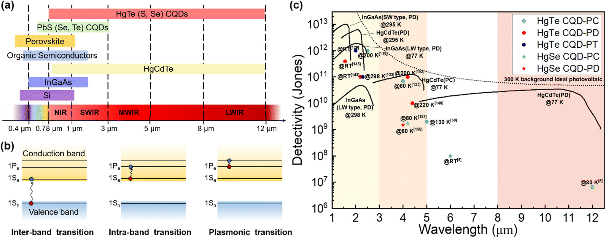 | ||
| Fig. 1 Advances of Hg chalcogenide QDs for IR sensing. (a) Reported photodetection ranges of the representative solution-processable semiconductors compared with the typical inorganic bulk materials with IR responses. (b) The IR absorption mechanisms of Hg chalcogenide QDs. (c) Sensitivity vs. sensing wavelength comparison of the reported best-performing Hg chalcogenide QD IR photodetectors with the state-of-the-art commercial products based on inorganic bulk materials. CQD: colloidal quantum dot; PC: photoconductor; PT: phototransistor; PD: photodiode; RT: room temperature; SW: short wavelength; LW: long wavelength. The data of the inorganic bulk IR photodetectors are adapted from ref. 8 with permission from the Society of Photo-Optical Instrumentation Engineers, copyright 2018. The data of LW-type InGaAs are adapted from ref. 9 (website from Hamamatsu Photonics K. K.). | ||
IR absorption of Hg chalcogenide QDs can be realized with both inter-band and intra-band transitions. Fig. 1b respectively illustrates the transition processes of inter-band and intra-band absorption, or even plasmonic transitions for heavily doped dots. For inter-band transition, the optical transition occurs between the highest valence band and the lowest conduction band, when the photon energy is larger than the energy gap between them. By natural or intentional doping, the 1Se state in the conduction band of the QDs could be partially or fully occupied to then facilitate transitions between the 1Pe and 1Se levels when the photon energy matches with the intra-band energy gap. These intra-band gaps are comparatively smaller than the adjacent inter-band gap, which is beneficial for long wavelength sensing. QDs based on HgTe, which is a semi-metal with a negative bandgap at the critical point in the Brillouin zone as a bulk material,10 have demonstrated controllable inter-band absorption tunable from the NIR to LWIR range varied by simple adjustment of the particle size. For HgS and HgSe QDs, with self-doped n-type properties above comparatively small particle diameters, the photo-sensing ability is more attractive via intra-band absorption in the MWIR range, and this obviates the need for large particle synthesis. Moreover, the Hg chalcogenide QDs can be further heavily-doped for plasmon resonance occurrence, which may relate to the multiple intra-band transitions between the quantized states above the 1Pe state.11,12 In the past decade, colloidal HgTe QD based IR photodetectors with inter-band absorption have attracted most research effort and demonstrated a series of promising applications with varied device structures. Meanwhile, intra-band photodetection using other Hg chalcogenide QDs is promising for longer wavelength absorption with smaller dots.13 Although these QDs contain heavy metal Hg, the Hg content in the thin-film based Hg chalcogenide QD photodetectors is very low and is sequestered in the form of a covalently bound material rather than volatile free metal or soluble leachable ionic compounds.
Fig. 1c is a comparison of the best-performing laboratory-fabricated Hg chalcogenide colloidal QDs (CQDs) with different device structures with the state-of-the-art representative commercial products (e.g., InGaAs detectors for the SWIR range and HgCdTe (MCT) devices for the MWIR range). In the SWIR range, the HgTe QD phototransistors/photodiodes have achieved the optimal trade-off between the sensitivity and the photo-sensing range compared to the commercial InGaAs photodetectors at room temperature (RT). In the MWIR range, the sensitivity of HgTe colloidal QD photodiodes is approaching that of epitaxial HgCdTe devices, with good tolerance at the operating temperature. For the photo-sensing range above 5 μm, the HgSe QD photodetectors with intra-band absorption may show some advances, while the sensitivity is still much lower than that of the current commercial products. Therefore, Hg chalcogenide QDs are highly promising candidates as solution-processed semiconductor materials to reach a breakthrough for the next-generation low-cost high-sensitivity and compact IR photodetectors, both in SWIR and MWIR ranges.
Previous reviews have provided a broad discussion about the synthesis and devices of narrow band QDs with IR light-emission, photo-response and thermal imaging properties.14–16 Gréboval et al. reviewed Hg chalcogenide QD devices both in IR sensing and light emission, focusing more on detailed discussion of the material aspects.17 Here, we offer a focused review on Hg chalcogenide colloidal QDs for IR photodetection, with a comprehensive summary about the essential progress of Hg chalcogenide QD IR photodetectors, from synthesis methods, property control to device engineering for different detector structure schemes, as per the outline diagram shown in Fig. 2. We illustrate how the device performances are optimized with the coordinative progress of each of the various factors from synthesis optimization, doping control, ligand exchange and the device fabrication strategy to finally contribute to the photo-sensing optimization encapsulated in different figures of merit. The imaging demonstrations and the compatibility of Hg chalcogenide colloidal QDs with focal plane arrays (FPAs) for high-quality imaging are discussed. Besides the photodetection performance optimization and wavelength range extension, Hg chalcogenide QD based IR photodetectors can be readily integrated with other material systems, photonic structures18 and scalable manufacturing processes.19 We also describe and summarize examples of a series of multi-functional, integrated, and flexible applications of these IR QDs. This review concludes with the prospects for optimization directions for Hg chalcogenide QD based infrared photodetectors and their commercialization route.
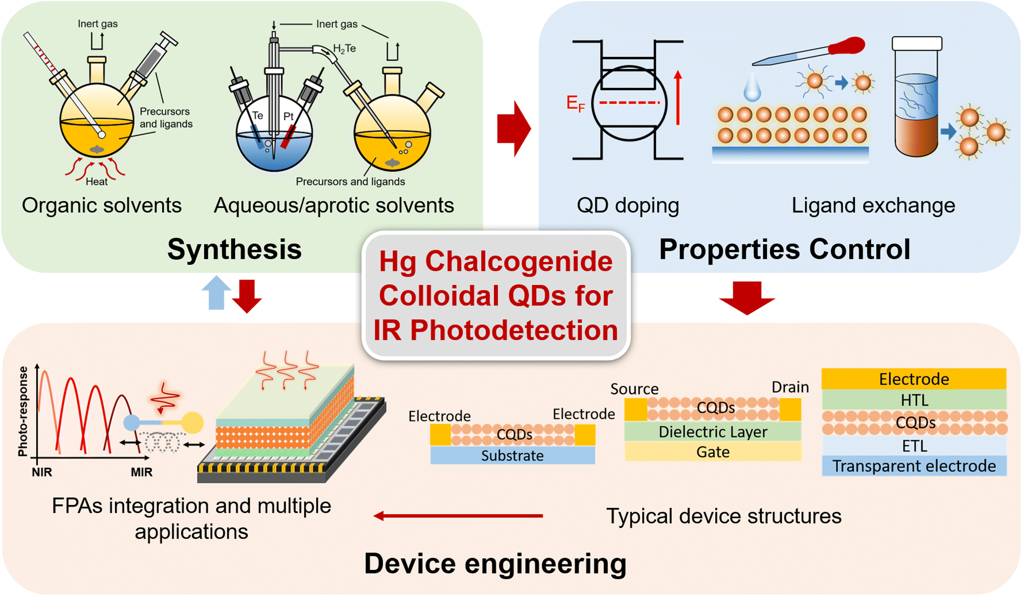 | ||
| Fig. 2 Outline diagram of this review. The essential factors that affect the device performance and applications of Hg chalcogenide QD based IR photodetectors include QD synthesis, property control for IR sensing and device engineering. | ||
2. Synthesis of Hg chalcogenide QDs
2.1. Synthesis in aqueous and aprotic solvents
The aqueous colloidal QD synthesis method popularized by Rogach and co-workers during the late 1990s for Hg- and Cd-chalcogenides20–23 (and their alloys24,25) can be traced back to earlier works by Weller's group26–28 and earlier still by Henglein's group.29–31 Whilst in earlier works, ligands such as polyphosphates were used, providing ionic stabilization,32 Rogach, working with Weller, led the switch to thiols and in particular thiolate-based ionic stabilization.33–37 Later work with HgTe QDs grown in water at high pH and using ligands such as 1-thioglycerol (1-TG) or other small mercaptoacids, etc.21–23,38 demonstrated that such low/zero bandgap materials could be size tuned from around an 800 nm band edge out into the SWIR range up to 1700 nm or so quite readily. Similar synthetic approaches were used to grow size quantized nanocrystals of other low bandgap materials such as HgSe and PbTe, although the photoluminescence quantum yields (PLQYs) of the inter-band transitions of these materials were rather lower (few %) than for HgTe QDs using this synthetic route.39 A number of studies on the optimization of this type of aqueous synthetic method for Cd- and Hg-chalcogenides were made during this period showing how the PLQY could be improved from the few to 10% range and then to 50% or more in many cases.21,36,37,40–43 For HgTe QDs, a variety of sources were used: H2Te gas could be generated in a separate flask and the gas was then blown into the reaction flask in a stream of inert nitrogen or argon. The gas could be generated by the action of mineral acids on tellurides such as Al2Te3, or by electrochemical methods with elemental Te as the cathode, as the typical synthesis setup of HgTe QDs in aqueous and aprotic solvents schematically shown in Fig. 3a. Other aqueous methods for HgSe and HgS QDs (and HgSexS1−x alloys) have included biomimetic methods with HgCl2 as the cation precursor and Na2SeO3 as the selenium precursor and glutathione as both the ligand and a slow release sulfur source.44–46 Whilst not entirely an aqueous method, several reports were made by Kuno and colleagues detailing the preparation of HgS and HgSe QDs via a micellar approach.47–49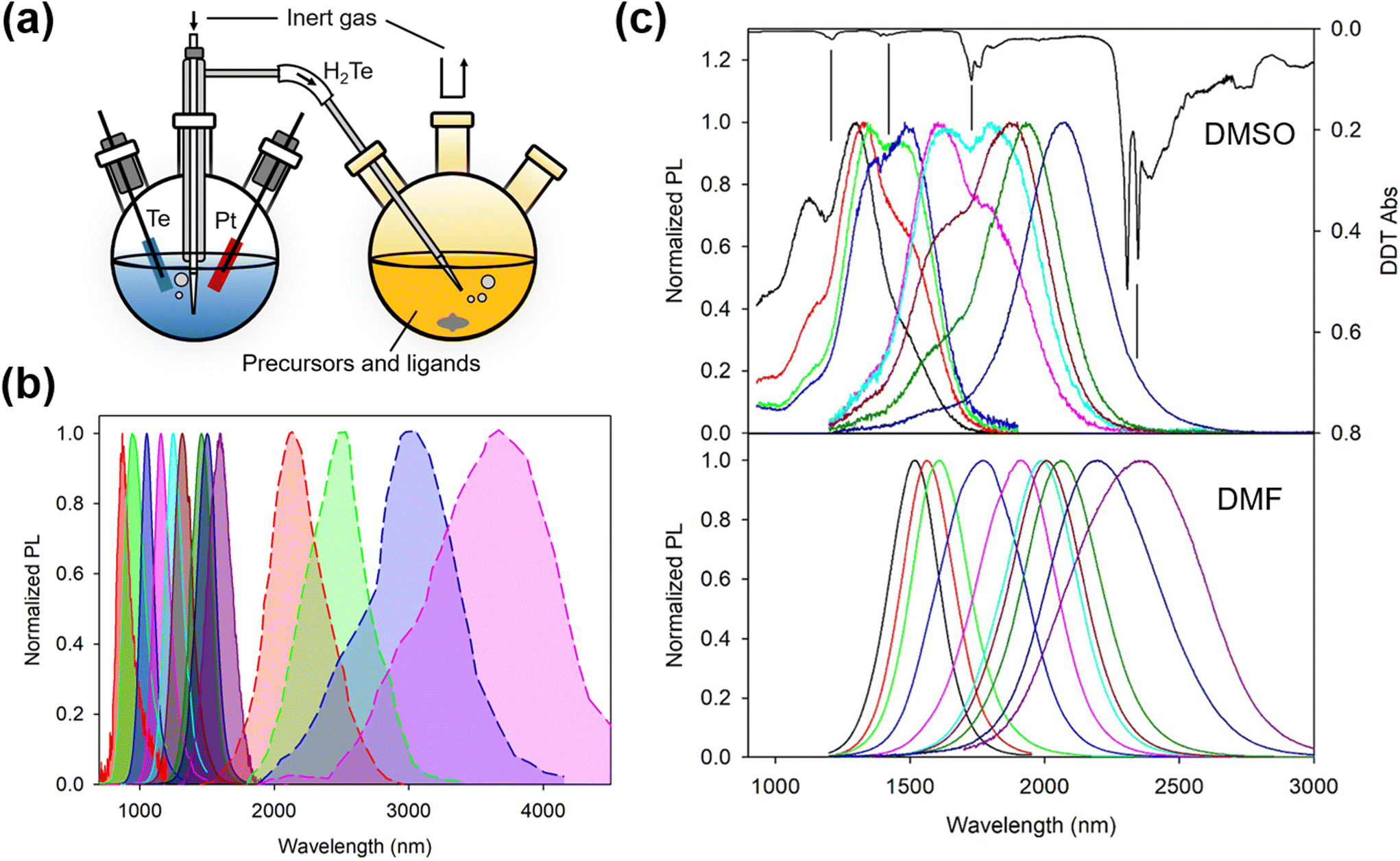 | ||
| Fig. 3 Synthesis of HgTe QDs in aqueous and aprotic solvents. (a) Typical synthesis setup in aqueous and aprotic solvents (note that in reality, oxygen is evolved at the Pt electrode so the latter is sleeved to allow the gas to be collected and to escape the electrochemical flask without it decomposing the H2Te gas liberated at the Te electrode). (b) Normalized PL spectra of HgTe QDs grown in water according to the method of ref. 38 with the central PL peak up to 1600 nm (previously unpublished data) and the enlarged HgTe QDs grown by Ostwald ripening in aqueous solution, which is reproduced from ref. 50 with permission from American Chemical Society, copyright 2006. (c) The influence of the growth aprotic solvent (DMSO and DMF) and the basicity of the reaction mixture used for the growth of similar sizes of HgTe QDs. Spectra for both solvents were recorded after the extraction of the QDs in TCE and ligand exchange from FMT to DDT. The dips in the DMSO grown solution coincide with the ligand DDT overtone and combination bands, as the inverted absorption spectrum of DDT (top-most black curve) is also shown for comparison. Reproduced from ref. 51 with permission from American Chemical Society, copyright 2020. | ||
In 2006 Kovalenko et al.50 pushed the aqueous synthetic method for HgTe QDs further by making use of a post-synthetic Ostwald ripening stage. Similar to the preceding work, they initially grew QDs with 1-TG or mercaptoethylamine (MEA) ligands, and after the addition of the H2Te precursor in a concentrated gaseous dose over a short time interval, immediately followed by a ripening stage at elevated temperature (typically 75–80 °C for several hours). In the case with MEA as the ligand they grew QDs at pH 4.1 and the weaker surface interaction allowed faster ripening and more ready replacement of the synthesis ligand with a long chain ligand, dodecanethiol (DDT) to facilitate the transfer of the QDs into the IR transparent solvent CCl4 for spectroscopic measurements. Whilst the aqueous slow growth of HgTe QDs into the 1000–1600 nm range could be carried out whilst reasonably restricting the polydispersity to below around 15% (PL full width at half maximum, normalized by the peak wavelength), the rapid growth kinetics entailed in the Ostwald ripening process generally led to much wider size dispersions (e.g. 30%), as shown in Fig. 3b. A size selective precipitation was adopted to refine and extract narrower size fractions from the broad distributions obtained after ripening;50 however, this approach is relatively difficult to replicate on a large scale and is rather time consuming.
To further extend the wavelength range of the as-grown HgTe QDs without the PLQY reduction during Ostwald ripening, aprotic solvents were adopted to replace water for the synthesis. Aprotic solvents are intermediate solvents which have the capability to solvate not only organic solutes but also some ionic solutes alongside them. In this set of solvents, dimethyl formamide (DMF) and dimethyl sulfoxide (DMSO) are frequently employed. They have wide liquid temperature ranges and so are suitable for synthesis at RT and above (up to 189 °C for DMSO and up to 153 °C for DMF). In connection with IR QD synthesis, the initial interest in using aprotic solvents was their compatibility with sol–gel synthesis in order to form hybrid QD–glass forming matrix materials for QD waveguide fabrication.39,52 For growth in DMSO, the metal salt used was Hg acetate and the ligand was furanmethanethiol (FMT). The tellurium precursor was electrochemically generated hydrogen telluride gas, bubbled into the reaction flask over a period of time that could range up to many hours depending on the reaction volume, reaction temperature and the final QD diameters required.53 Synthesis in DMF gave better results by comparison.51 Whilst the method was broadly similar to that in DMSO, it was possible to use rather stronger organic bases such as triethylamine (TEA) or tripropylamine (TPA) which were not suitable for use with DMSO. With these bases, H2Te formed a more stable HTe− salt resulting in less decomposition and better absorption of the gas during the reaction. Fig. 3c is the comparison of the PL spectra of HgTe materials produced in the two solvents, where the QD sizes and their measurement environments were identical. The reduction in the overtone and combination dips in the PL spectra of the DMF grown material was interpreted to have stemmed from a reduction in the density of surface traps and reduced polaron formation between trap localized charge carriers and the vibrational modes of surface adjacent ligands.54
2.2. Synthesis in organic solvents by hot injection and related methods
In 2003 Green et al.55 and later Piepenbrock and co-workers56 paved the way for the synthesis of Hg-chalcogenides in organic solvents, using metal salts with a weakly coordinating solvent such as oleylamine, instead of the highly toxic mercury alkyl compounds (e.g. dimethyl mercury).57 The tellurium precursor was the TOP![[thin space (1/6-em)]](https://www.rsc.org/images/entities/char_2009.gif) :Te complex and TOPO (TOP: trioctylphosphine; TOPO: trioctylphosphine oxide) was present as a further surface coordinating species. Green's group later extended their method to produce HgSe QDs in a RT reaction,58 and cubic (β-) HgS QDs using a hot (120 °C) injection type synthesis.59 In 2011 Keuleyan et al. first reported the IR photo-response of Hg-chalcogenide QDs in the MWIR range, which were synthesized by hot-injection with the combined characteristics of earlier synthesis methods in organic solvents.60 They grew HgTe QDs using a mercury acetate precursor in butanol/pyridine mixed solvent and either TOP:Te (for larger QDs) or tributylphosphine (TBP):Te (for smaller dots) in butanol as the injected Te precursor, with a hot-injection setup typically shown in Fig. 4a. The reaction was relatively small scale (<10 ml) and the injection was made at temperatures of up to 90 °C. After short reaction times, typically a few minutes, the reactions were quenched by adding DDT and cooling the aliquots to RT, with the QD emission peak wavelengths of up to 5 μm. This method evolved with the replacement of the butanol/pyridine solvent medium with oleylamine and the more readily soluble metal chloride instead of the acetate salt, with the QD size being controlled by varying the reaction temperature across the range from 60 °C to 100 °C.61 Whilst the emission ranges of the HgTe QDs obtained were similar to those in their earlier work, the polydispersity was significantly lowered, improving the sharpness of the absorption band edge, as per the evolved PL and absorption spectra shown in Fig. 4b and c. Later reports replaced oleylamine with octadecylamine (ODA), to optimize the batch repeatability,62,63 and the QD diameters were increased to 20 nm and the inter-band edge shifted to around 12 μm with their regrowth method.5
:Te complex and TOPO (TOP: trioctylphosphine; TOPO: trioctylphosphine oxide) was present as a further surface coordinating species. Green's group later extended their method to produce HgSe QDs in a RT reaction,58 and cubic (β-) HgS QDs using a hot (120 °C) injection type synthesis.59 In 2011 Keuleyan et al. first reported the IR photo-response of Hg-chalcogenide QDs in the MWIR range, which were synthesized by hot-injection with the combined characteristics of earlier synthesis methods in organic solvents.60 They grew HgTe QDs using a mercury acetate precursor in butanol/pyridine mixed solvent and either TOP:Te (for larger QDs) or tributylphosphine (TBP):Te (for smaller dots) in butanol as the injected Te precursor, with a hot-injection setup typically shown in Fig. 4a. The reaction was relatively small scale (<10 ml) and the injection was made at temperatures of up to 90 °C. After short reaction times, typically a few minutes, the reactions were quenched by adding DDT and cooling the aliquots to RT, with the QD emission peak wavelengths of up to 5 μm. This method evolved with the replacement of the butanol/pyridine solvent medium with oleylamine and the more readily soluble metal chloride instead of the acetate salt, with the QD size being controlled by varying the reaction temperature across the range from 60 °C to 100 °C.61 Whilst the emission ranges of the HgTe QDs obtained were similar to those in their earlier work, the polydispersity was significantly lowered, improving the sharpness of the absorption band edge, as per the evolved PL and absorption spectra shown in Fig. 4b and c. Later reports replaced oleylamine with octadecylamine (ODA), to optimize the batch repeatability,62,63 and the QD diameters were increased to 20 nm and the inter-band edge shifted to around 12 μm with their regrowth method.5
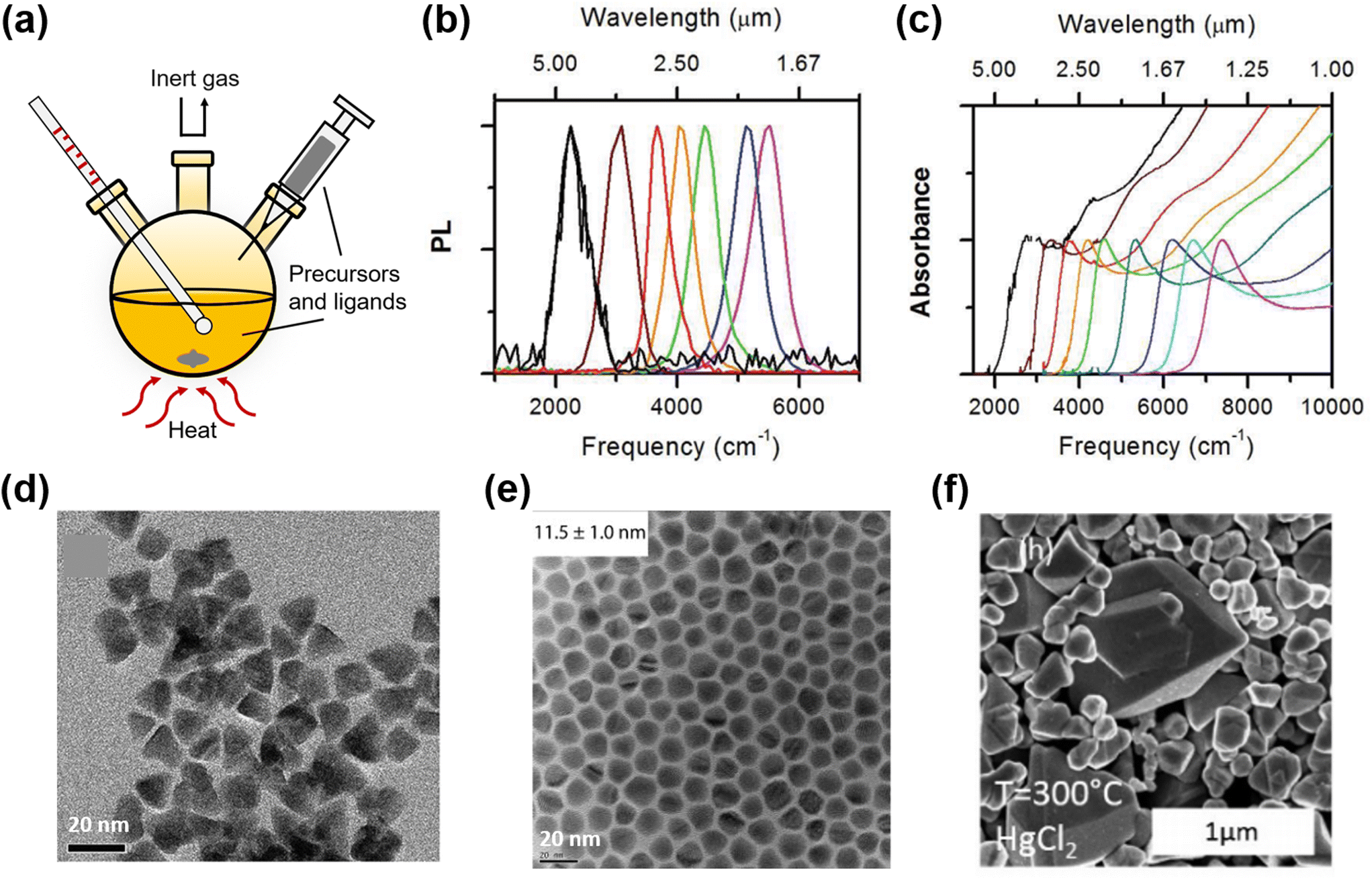 | ||
| Fig. 4 Synthesis of HgTe QDs in organic solvents with the hot-injection method. (a) Typical hot-injection synthesis setup with organic solvents. Normalized PL (b) and absorption (c) spectra of HgTe QD solution in C2Cl4 (C–H absorbance of the ligands is subtracted for clarity) (d) TEM image of HgTe nanoparticles in tetrahedral shape. (b–d) Are reproduced from ref. 61 with permission from American Chemical Society, copyright 2011. (e) TEM image of non-aggregated HgTe QDs in spherical shape. Reproduced from ref. 65 with permission from American Chemical Society, copyright 2017. (f) SEM image of HgTe QDs synthesized at 300 °C using HgCl2 as the precursor, with absorption in the THz range. Reproduced from ref. 7 with permission from American Chemical Society, copyright 2018. | ||
The Guyot-Sionnest group has developed the HgTe synthetic method further by the use of a more reactive Te precursor, i.e. bis(trimethylsilyl) telluride ((TMS)2Te), which has benefits in terms of QD shape control (spherical versus (truncated) tetrahedral)64 and a reduced tendency to aggregate at larger particle sizes during synthesis in addition to allowing the emergence of air-stable n-type doping to be observed in larger particles65 and for higher energy inter-band transitions to be better resolved.66 The TEM images of partially aggregated HgTe QDs with tetrahedral shape61 and the monodisperse QDs with spherical shape65 are compared in Fig. 4d and e. Single step hot injection syntheses using HgCl2 as the metal precursor in oleylamine and injecting the telluride precursor at between 70 and 120 °C could tune the QD particle size between 5 nm and 13 nm and yield spherical particles, whereas the use of TOP:Te under similar circumstances would yield tetrahedral particles and require longer reaction times for a given particle size.66 They also synthesized HgSe QDs with a similar hot-injection method, and oleylamine has most frequently been used as the base solvent with HgCl2 as the metal precursor, and selenourea67 (or derivatized selenourea68) was used as the Se precursor. The Se precursor was typically injected into the reaction mixture at 110 °C to yield over 6 nm diameter HgSe QDs with 16 min growth time,69 but larger particles could be obtained at higher reaction temperatures or with extended growth stages.70 For HgS QDs, commonly HgCl2 was used as the cation precursor and oleylamine as the solvent in conjunction with (TMS)2S as a conveniently reactive precursor source.71,72 The reactivity of these sulfur precursors influenced the QD diameters obtained, with the more reactive (NH4)2S source yielding the largest sizes.73
In 2018, the Lhuillier group revisited the TOP:Te hot injection method but took a critical look at how the reaction evolved for wider ranges of reaction times and reaction temperatures and for different mercury halides.7 Rather than injecting their TOP:Te containing solution into a hot oleylamine solution of the metal salt, both precursor solutions were mixed together at RT and the combined precursors were promptly injected into hot oleylamine, ensuring intimate mixing of the two halves of the reaction from the outset. Reaction temperatures were also varied from 80 °C to up to 300 °C, where even a short 3 min reaction could yield particles with mean sizes in the 200 nm size range, as shown in the SEM image of the nanocrystals in Fig. 4f. The IR absorption feature was extended from MWIR and LWIR to the THz range: first an inter-band transition occurred followed by red shifting with increasing size, and then at large sizes, an intra-band transition also emerged.
Most syntheses of Hg chalcogenide QDs in organic solvents had used either Hg acetate or halides as the mercury source, although more readily soluble organic anions, such as propionates, myristates, etc., had become popular for 2D nanoplatelet syntheses.74 In 2020, Goubet et al.75 introduced the use of Hg-thiolates (e.g. Hg-dodecanethiolate) as an alternative metal precursor. These could be prepared separately prior to the reaction and added to the oleylamine solution in the flask prior to the injection step. Alternatively, Hg-thiolate could be produced in situ in the reaction flask by sonication of liquid mercury in the presence of DDT. Oleylamine and a certain amount of iodine (to ensure the oxidation of Hg0 to HgII) were added and this mixture was warmed and used in the QD reaction where the TOP:Te solution was injected. Without iodine, the QDs formed in the reaction tended to fuse together into rod-like structures during growth. This reaction was also demonstrated at scale, with 7 g of QD product obtained, which is favoured for commercial-scale production.
3. Control of properties for IR sensing
For the low and zero-bandgap Hg chalcogenide QDs used in IR sensing, QD doping is an essential property to be controlled to modulate the predominant carrier type and in the case of n-type doping of the lower 1Se and even 1Pe states to access intra-band transitions. When the Fermi level lies between the valence and conduction bands, QDs may exhibit weak p-type behaviour through ambipolar and eventually move towards n-type carrier behaviour. If the Fermi level is positioned near the conduction band or within the conduction band itself (and even amongst the higher electron states), the carrier type may shift to being firmly n-type and rather than showing inter-band optical transitions may show only intra-band characteristics. For very high conduction occupancy, the electronic nature of the QDs may become plasmonic in nature.7 In Hg-chalcogenide QDs, degenerate doping is controlled through the manipulation of the QD size, stoichiometry (which is also coupled to the QD size) and through shifts in the Fermi level relative to the conduction band brought about by the changes in dipole effects due to ligand substitutions. The ligand substitution process also strongly affects the carrier mobility of the deposited solid film, which is an essential factor that affects the IR sensing performance in device demonstration. In this section, we will first discuss QD doping with the manipulation of the size and stoichiometry, which is directly related to the intra-band absorption of Hg chalcogenide QDs. Then, we will summarize the ligand exchange methods adopted for Hg chalcogenide QDs and the corresponding tunability of QD films.3.1. QD doping for intra-band transitions
Due to the smaller work functions relative to those of comparably sized HgTe QDs, the Fermi level approaches the conduction band as the QD diameter is increased, allowing n-type self-doping properties to be accessed, as was first observed in HgSe and β-HgS QDs. Although n-type self-doping in HgS QDs has received less attention than in the exploration of HgSe QDs, it was first studied as far back as 2014 by Jeong et al.73 The transfer of oscillator strength between the inter-band and intra-band transitions by electrochemically modulated doping was demonstrated for intermediate sized QDs. In addition, for dots that were initially sufficiently large and therefore n-doped enough to show an intra-band transition, the successive deposition of alternating monolayers of S2− and Hg2+ ions was able to turn the inter-band transition on and off (and vice versa the intra-band transition). This was one of the first reports to reconcile the variation in doping to the shift of the conduction and valence band levels relative to the Fermi level. In 2016, the intra-band transitions from higher quantum states were observed in heavily n-doped HgS QDs,72 as shown in Fig. 5a. One or more of the lower electronic states, e.g., 1Se, 1Pe, can be partially or fully occupied if the Fermi level can be sufficiently raised above these levels. This can then allow the intra-band transitions such as 1Se–1Pe and 1Pe–1De to be seen in the IR absorption spectra and to be accessed. The difference in these energy levels is a lot lower than the 1Se–1Sh inter-band transition and so these intra-band transitions are useful in longer wavelength photodetection with relatively smaller dots (Fig. 5b).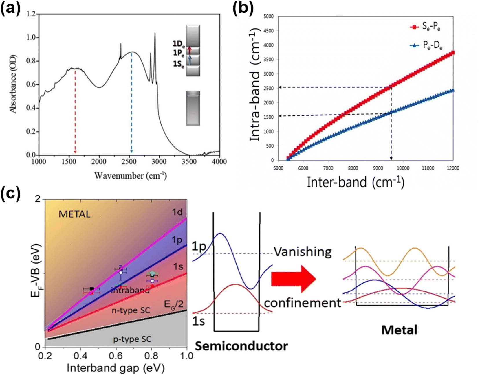 | ||
| Fig. 5 Intra-band transitions of HgS and HgSe QDs. (a) Intra-band transitions (1Se–1Pe and 1Pe–1De) for n-doped HgS QDs. (b) Comparison of the inter-band and the first intra-band transition energies for a given size calculated for HgS. (a and b) Are reproduced from ref. 72 with permission from American Chemical Society, copyright 2016. (c) Successive filling of the lower electron excited states results in increasing n-doped characteristics. p-Type behaviour gives way to ambipolar, then n-type (introducing the possibility of intra-band transitions as the 1Se level is filled), and eventually plasmonic behaviour at higher occupancies. As the QD size increases and the inter-bandgap energy decreases, these transitions in behaviour occur at lower energies. The data points correspond to QDs of various sizes and ligand doping treatments. Reproduced from ref. 78 with permission from American Chemical Society, copyright 2017. | ||
One of the earliest reports of n-type HgSe QDs was by Yun et al.76 in 2010. They reported the use of aqueous grown sintered p-type HgTe QDs and n-type HgSe QDs in complementary field effect transistor (FET) logic circuit fabrication. Using an organic hot injection method, Deng et al.67 synthesized 5–7 nm HgSe QDs and likewise observed n-type behaviour and clear intra-band transitions when the 1Se state was occupied via self-doping. This could be suppressed to various degrees by surface sulfide addition using a colloidal atomic layer deposition (ALD) treatment of (NH4)2S such that the 1Se occupancy could be correlated with the extent of sulfide deposition. In 2017 Jeong et al.69 further explored n-type doping in the same material to demonstrate the level filling progression in the 1Se state from none, single and double occupancy as the size increased. The intra-band transitions could then be restored by a further treatment with the Hg salt, leading to the conclusion that the Hg rich surface was a key factor in the n-type character of the as-grown dots. In the course of growing a selection of different sized HgSe QDs for subsequent addition of CdSe and CdS shells by c-ALD, Sagar et al.77 observed that by the time the QD size increased to 4.3 nm, the absorption spectrum had both inter- and intra-band features indicating that the 1Se level was starting to be occupied in larger dots. During the c-ALD process to add alternate layers of Se and Cd it was observed that the n-type doping could be altered to give an ambipolar or intrinsic charge carrier characteristic, even for the larger core diameter core/shells.
In 2017 Martinez et al.78 pursued the HgSe self-doping theme further on a wide range of QD sizes from 4.5 nm, 5.8 nm, 15–17 nm, to above 20 nm. XPS and optical studies revealed the impact of different ligands and QD sizes on the band alignments of the valence band, and the 1Se, 1Pe, 1De and the vacuum levels versus the Fermi level. Coupled with transistor measurements, they were able to propose a phase diagram as shown in Fig. 5c (Fermi level-valence band offset vs. the inter-band energy gap for each doping case), showing the transitions from p-type through intrinsic, n-type, and at very high electron doping levels, e.g., >18 electrons per dot, the onset of plasmonic behaviour. They later demonstrated a method to substantially de-dope the HgSe QDs (from 5 electrons per dot to around 0.03 electrons per dot) by the grafting of a thiol functionalized polyoxometalate onto the dots, showing how the intra-band transition could be switched to an inter-band transition.79 In 2019 Melnychuk et al. investigated the optical properties of n-type HgSe QDs with various sizes from 4.4 to 9.1 nm.70 For the largest particles they conclude that the doping was sufficient to put them at around 15 electrons per dot and close to the onset of plasmonic behaviour. For the smaller, lightly-doped 5 nm QDs they observed the suppression of Auger relaxation in the intra-band transition owing to the reduced densities of states involved compared with the inter-band transitions, which may favour IR sensing applications in high operating temperature cases.
Stemming mostly from the relatively large work function,80 the earlier reported HgTe QDs mainly exhibited inter-band transitions, with the electronic charge transfer properties revealed by FET studies to be p-type,81,82 weakly p-type2 or ambipolar.60,83,84 These QDs generally had inter-band transitions below 5000 nm and the QDs were mostly tetrahedral (or in some cases tetrapodal). The p-type characteristic was retained when the deposited QD films were sintered to form more conductive nanocrystalline films.76,82,85 Lhuillier et al.86 compared the carrier characteristics under air-free processing conditions and with the additional coating of As2S3, versus processing under ambient conditions and concluded that the p-type behaviour of small sized HgTe QDs frequently observed may have been a product of surface oxidation. With their air-free processing method they could observe contrasting ambipolar responses from the same QD aliquots.
With the synthesis modifications of organically grown HgTe QDs to change the shapes to be more spherical than tetrahedral, and to better control size distributions whilst also accessing larger QD sizes, in 2017, Shen et al.65 grew dots in the 4.8 nm to 11.5 nm size range and observed air-stable n-type self-doping. They suggested that both the reduced faceting (spherical shapes) and the use of excess Hg-precursor led to a Hg rich surface (e.g. Hg:Te ratios up to 1.4–1.5) with some of the excess precursor acting in effect as Hg2+ ligands at the surface of the QDs. A similar synthetic method was used by Hudson et al.66 to produce HgTe QDs in the 5–13 nm range. Again, air-stable n-type doping was observed and consequently several distinct intra-band transitions could be resolved thanks to the low size polydispersity obtained by post-synthetic size selective precipitation. They assigned the intra-band features to transitions between the 1Se state and various split 1Pe states (Fig. 6a), with the splits arising because of slight asymmetry in the particle shapes (truncated cubes, close to spherical but not perfectly so). The intra-band absorption shifted with the QD size and the doping level, and up to 2 electrons per dot injection were demonstrated (Fig. 6b). The n-type character of the as-synthesised QDs could be reversed to ambipolar (intrinsic) and an inter-band transition could be observed after the mild oxidation of the QD surface using molecular iodine.
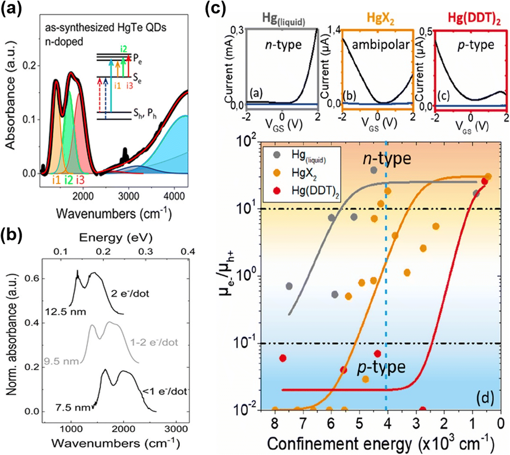 | ||
| Fig. 6 Intra-band transitions of HgTe QDs. (a) Absorption spectrum of the n-doped HgTe QD spectrum to a sum of Gaussians indicates that doping suppresses the excitonic transitions and induces intra-band absorbance (i1–i3). The experimental data are shown by a bold black line, and the fit is shown by a red line. (b) The intra-band absorbance for different sizes of QDs with different doping levels has similar spacing and relative intensity for the three peaks, but the peak positions shift with size. (a and b) Are reproduced from ref. 66 with permission from American Chemical Society, copyright 2018. (c) Upper panels: transfer curves of HgTe QD films with excitonic features at around 4000 cm−1 synthesized with liquid mercury, mercury halide, and mercury-(bis)dodecylthiolate with drain–source current (black) and gate–source current (blue). Bottom panel: mobility ratio of electrons and holes of HgTe QDs synthesized using different mercury precursors with different confinement energies (taken equal to the inter-band transition energies). Reproduced from ref. 75 with permission from American Chemical Society, copyright 2020. | ||
Goubet et al. further investigated the self-doped properties of HgTe QDs and nicely completed the understanding and highlighted some subtleties with QD diameters from 5 nm to over 200 nm.7 For S2− capped HgTe QDs in electrolyte gel gated FET devices, as the size of the QDs increased a transition from p-type through ambipolar to n-type behaviour (corresponding to a doping level of up to 6 electrons per dot) was shown, bringing the n-type doping capability of HgTe QDs onto a similar basis of HgSe and HgS QDs. In a more recent study, the transition from p-type to n-type vs. size was examined with types of synthetic methods, in particular the Hg precursors used.75 There were three cases: a Hg thiolate precursor generated in situ from liquid Hg sonicated in the presence of DDT, Hg thiolate prepared prior to the synthesis and used after purification, and the use of Hg halides. These three synthetic methods overlapped to some degree in the size of QDs they could produce, and again as the size increased a transition from p-type through ambipolar to n-type was observed. However, the diameters at which these transitions occurred were slightly different for the three different growth techniques (Fig. 6c). This was interpreted as there being slight differences in the stoichiometric Hg:Te excess arising from the use of different Hg precursors, which could occur due to different degrees of surface faceting (e.g. deviation from pseudo-spherical shapes) in the dots obtained by each growth method.
3.2. Ligand exchange
Ligand exchange is a widely-adopted post-synthesis treatment method for QDs for characterization and device fabrication, with the functions (i) to transfer the QDs into suitable ligands and solvents for optoelectronic characterization, (ii) to control the majority carrier type with shifts in the Fermi level, and (iii) to tune the charge mobility in the resulting solid-film deposited for device applications. For the aqueous QDs capped with short thiol ligands, the conductivity of the as-deposited films can be high enough for photo-response characterization. However, for the organic QDs capped with long alkyl ligands, the simply dried films are too insulating and have very poor carrier mobility, which makes the ligand exchange a necessary treatment. There are two ligand exchange methods frequently adopted in Hg chalcogenide QDs, the in-film exchange process to replace the ligands of the QDs as deposited, and the solution phase ligand exchange before the solid-film deposition.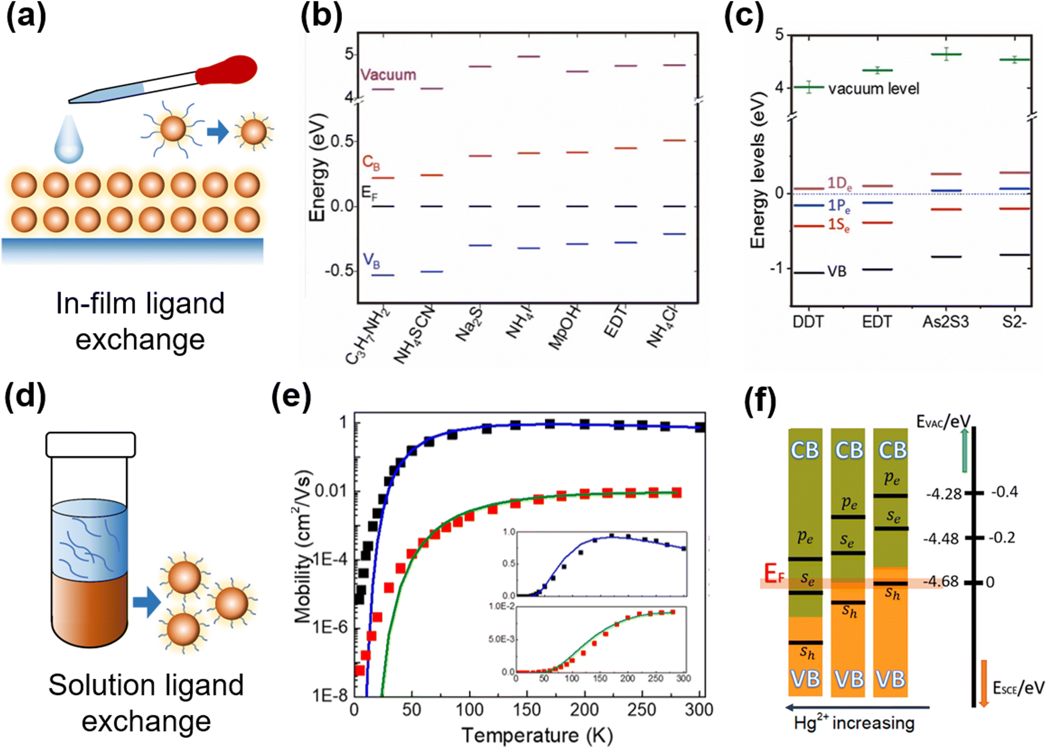 | ||
| Fig. 7 Ligand exchange and property control of QD films. (a) Schematic of in-film ligand exchange. Various surface ligand induced shifts in the conduction and valence band levels relative to the Fermi level (taken here as 0 eV with reference to all the other energy levels) for (b) HgTe and (c) HgSe QDs with in-film ligand exchange. (b) Is reproduced from ref. 100 with permission from American Chemical Society, copyright 2019. (c) Is reproduced from ref. 78 with permission from American Chemical Society, copyright 2017. (d) Schematic of solution phase ligand exchange. (e) Temperature-dependent FET mobilities of HgSe QDs with hybrid (black) and EDT (red) ligands, solid fitting curves are for Marcus theory of charge hopping. Reproduced from ref. 90 with permission from American Chemical Society, copyright 2020. (f) Controlling doping with HgCl2 concentration in solution ligand exchange. Reproduced from ref. 101 with permission from American Chemical Society, copyright 2019. | ||
The shifts in the Fermi level brought about by ligand substitutions, arising from changes in the ligand dipole interactions at the QD surface, are relatively small compared to the shifts in the conduction and valence band levels themselves due to the changes in the QD size. However, the ligand induced Fermi level shifts become more significant as the inter-band gap decreases and the conduction band itself is shifted closer to the Fermi level. Examples of the ligand dipole induced shifts of the relative Fermi level positions for a selection of ligands for HgTe and HgSe QDs are respectively given in Fig. 7b and c. Although the shifts are small, they are still proportionately significant in low bandgap materials, particularly for large QDs, and in these QDs they open up the possibility of intra-band absorption if the Fermi level falls within the conduction band(s). The choice of ligand is however also dictated by the carrier transport in the films of such materials and also the compatibility of that ligand with the film and device fabrication process.
For the Hg chalcogenide QDs grown in organic solvents and capped with long alkyl chain synthesis ligands such as oleylamine or DDT, multiple deposition and crosslinking via solid-film ligand exchange is quite time consuming and the ligand exchange is normally not entirely complete.105 The solution-phase ligand exchange was first adopted to examine the clean exchanges between the different organic solvent compatible ligand classes and doping level control, in HgSe QDs,79,106 HgS QDs,72 HgTe QDs,99 and HgSe/CdSe/HgSe NPLs.107 Then, this method was developed to produce HgTe QD inks, capped with short ligands in solvents such as DMF or N-methylformamide (NMF) for direct film deposition in IR sensing devices.108 The exchange of the long alkyl ligands is typically for Cl−, S2− ions or As2S3. As per the solution ligand exchange schematically shown in Fig. 7d, the QDs were taken at a high concentration (e.g., 50 mg ml−1) in toluene or similar hydrocarbon solvents, mixed well with e.g., HgCl2/mercaptoalcohol in DMF and NaS2 (or As2S3) in NMF, and stabilized for phase separation. Extra hexane was added to assist in driving the ligand exchanged QDs over into the lower, polar formamide phase. The dots in the lower phase were washed several times and redissolved in pure DMF or NMF at a high concentration to provide the QD ink. Chen et al. offered the caution that aggregation may need to be avoided in the final ink product and suggested a slightly different transfer method.90,101,109 They took well dispersed oleylamine capped HgTe QDs65 in hexane solution and exchanged them against a mixture of HgCl2, mercaptoethanol, butylamine and butylammonium chloride in DMF. They found that this mixture only required gentle shaking to initiate the transfer from hexane to the lower DMF phase. Then the QDs were precipitated and redissolved at a high concentration in DMF as an ink for film deposition. The above described HgCl2 based hybrid ligands efficiently eliminated the surface defect states, significantly boosting the carrier mobility in the as-deposited HgSe QD90 and HgTe101 QD films, as shown by the comparison of the temperature-dependent mobility with the QDs capped with EDT ligands in Fig. 7e. Controllable n- and p-doping of QDs could be realized by adjusting the concentration of HgCl2 (Fig. 7f). The HgTe QD films with hybrid ligands showed a band-like behaviour of mobility (dμ/dT < 0) down to 77 K, and reported a mobility of up to 8 cm2 V−1 s−1 with a low carrier density in lightly-doped QDs (<1 electron per dot). The resulting high mobility Hg chalcogenide QD films were applied in a series of photo-sensing structures from photoconductors, phototransistors to photodiodes to facilitate the photodetection performance, which will be described in the device engineering part.
4. Device engineering for IR sensing
4.1. Typical device structures and important figures of merit
According to the device structures, the Hg chalcogenide QD based photodetectors could be roughly classified into different schemes of photoconductors, phototransistors and photodiodes, as the typical device structures illustrated in Fig. 8a–c. Both the photoconductor and phototransistor are typically planar structures fabricated by directly depositing the light absorbing QD films onto normal substrates or dielectric layers with two (usually interdigitated) electrodes (one termed the source and the other the drain depending on the current direction). The photodetection ability of the photoconductor originates in the conductance change of the semiconducting film with the light illumination level, measured under an externally supplied voltage bias across the electrodes, which is closely related to the photoconductive gain mechanism as shown in Fig. 8d. Under illumination, electrons (holes) of the photogenerated carrier pairs can be temporarily captured by shallow traps. Then holes (electrons) could be driven by the external applied electric field to cycle in the circuit, until after a number of circulations they recombine with the released counter-charged carriers from the trap states. Therefore, one photogenerated electron–hole pair may produce multiple times the primary photoelectric current, with the multiplier being termed the photoconduction gain G. If we assume that the time for cycling once in the circuit is tc, the trap lifetime is τt, the applied voltage is V, and the distance between the electrodes is L, then the photoconduction gain can be expressed as G = τt/tc = τt·μ·(V/L2).110 That is, the photo-response properties are strongly associated with the lifetime(s) of the trap states and the charge carrier mobility, μ, in photoconductors. Considering the existence of multiple types of traps (with different depths and concentrations), the photoconductive gain is normally highly dependent on the illumination level.84,111 This reduces the linear dynamic response range (LDR) of the photoconductive devices but contributes to a high responsivity under weak light illumination.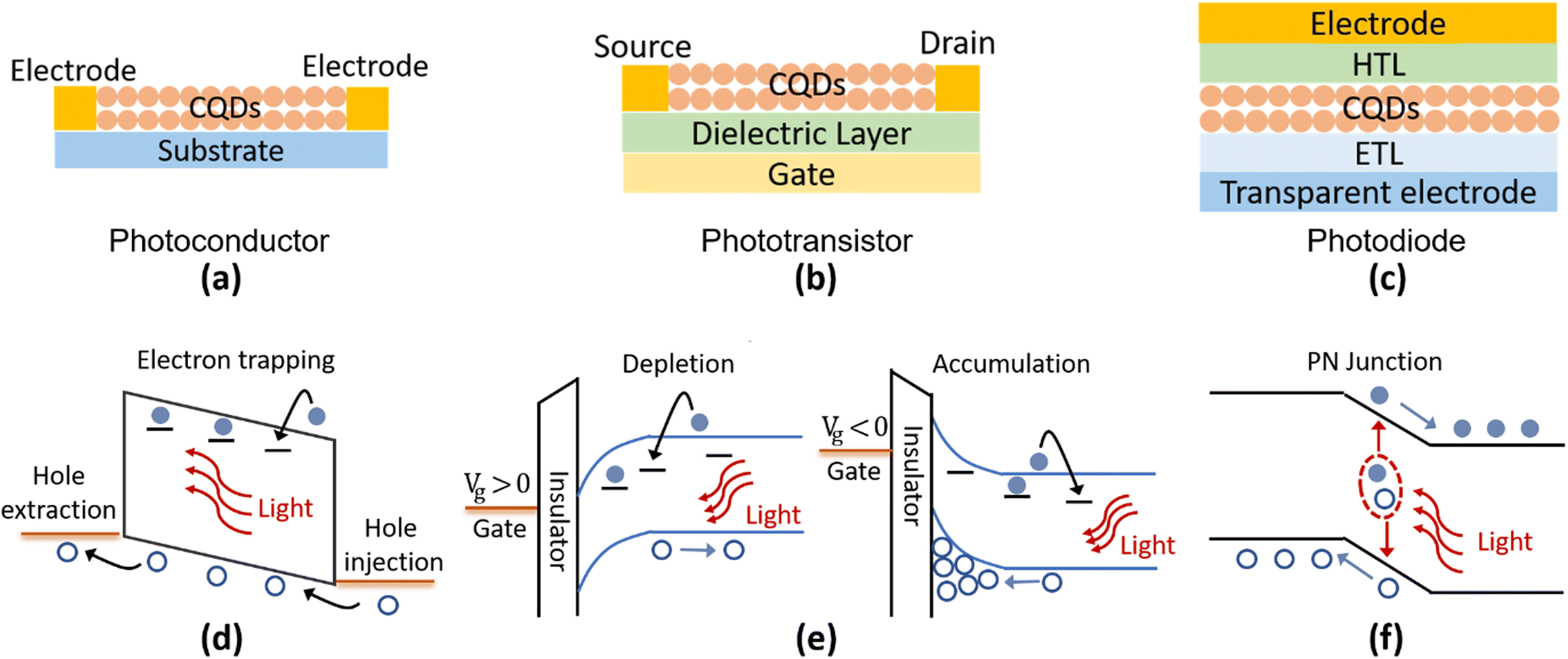 | ||
| Fig. 8 Typical photo-sensing device structures and their operation mechanisms. Schematic of typical photo-sensing device structures (a–c) and operation principles in different photo-sensing structures (d–f). Photoconductors and phototransistors are illustrated with p-type CQDs as examples in (d) and (e). | ||
With a similar photoconductive gain mechanism to photoconductors, the phototransistors are typically three-terminal devices with the additional control of a gate voltage. The gate is isolated from direct contact with the drain source conduction channel by a thin dielectric layer such as silicon dioxide or other insulating oxides. Through the gate voltage modulation of the carrier density in the conducting channel between the source and drain, the QD phototransistor can be operated in depletion or accumulation states to obtain a lower dark current or a higher photoconduction gain, as illustrated in Fig. 8e. Therefore, the phototransistors provide a versatile approach to control the carrier distribution and charge transport with gate voltage tuning, so as to affect the photodetection properties.
A Hg chalcogenide QD photodiode typically has a vertical multi-layer geometry, which is similar to photovoltaic devices. The QD film, as the photoactive layer, is frequently sandwiched by an electron transport layer (ETL, or an n-type layer) and a hole transport layer (HTL, or a p-type layer) to form a junction-like structure. A Schottky diode can also be formed with a QD/metal electrode contact without the ETL or HTL. As shown in Fig. 8f, with a strong built-in field at the junction area, the photogenerated electron–hole pairs can be rapidly separated and captured by opposite electrodes. This offers the advantages of a fast-transient response (also related to the device capacitance), a large LDR, and a low noise level as the devices could be operated under zero bias, which is favoured in commercial applications.
The important figures of merit for photodetection are summarized in Table 1,112,113 with the external quantum efficiency (EQE) and responsivity (R), relating to the photoelectronic conversion ability, noise equivalent power (NEP) and detectivity (D*), defining the sensitivity, 3 dB bandwidth (f3dB), the bandwidth limiting the modulation frequency, and the LDR revealing the measurable optical power range. To give a fair comparison of the sensitivity of different photodetectors with a diverse range of noise levels and sensing areas, the comprehensive parameter D* is normally employed. The noise equivalent temperature difference (NEDT) is a special figure of merit for thermal imaging systems to evaluate the minimum temperature difference that could be measured.113 In IR photodetection, especially in the MWIR and LWIR ranges, the concept of background-limited IR photodetection (BLIP) needs to be referred to ref. 8. Under ambient conditions, the photocurrent generated by the photon flux generated from blackbody emission contributes to a substantial proportion of the background signal. For instance, the emission peak of 300 K blackbody is in the region of around 10 μm and the spectral width of the blackbody peak can be quite substantial, so any integrated overlap with the responsivity curve can be a significant factor. Therefore, BLIP indicates that the noise level is limited by the background radiation. The combination of dark current and the related noise level that originated from the background blackbody radiation gives rise to the achievable sensitivity limit of an IR photodetector.
| Quantity | Symbol | Unit | Definition |
|---|---|---|---|
| Responsivity | R | A W−1 | The ability of a photodetector to transform incident light into output current, defined by the ratio of photocurrent (Iph) to the incident power of light on the detector (P0) at a given wavelength (λ) with Rλ = Iph/P0 |
| External quantum efficiency | EQE | % | The efficiency of a photodetector to transform the incident photons into electrons to be collected. Assuming that Np and Ne are the numbers of input photons and electrons produced per second, respectively, the spectral EQE can be calculated as: EQEλ = 100·(Ne/Np) = 100·(Iph/P0)(hc/eλ), where e is the electric charge, h is the Planck's constant, and c is the light velocity in a vacuum |
| Noise-equivalent power | NEP | W Hz1/2 | The minimum detectable radiant power, defined by the incident radiant power necessary to produce a signal-to-noise ratio of one. NEP = In/R, where In is the noise current spectral density with the unit A Hz−1/2 |
| Specific detectivity | D* | cm Hz1/2 W−1 (Jones) | A comprehensive parameter to compare different photodetectors, defined as the inverse of NEP with normalization to the unit detection area, D* = A1/2d/NEP = R(A1/2d)/In, where Ad is the effective detection area |
| 3 dB bandwidth | f 3dB | Hz | Maximum operational bandwidth, defined by the frequency at which the measured signal power reduces to 50% of its original response |
| Linear dynamic range | LDR | dB | The highest (Pmax) and the lowest (Pmin) light power at which the device can maintain a linear response to the light intensity, which can be calculated as LDR = 20log(Pmax/Pmin) |
| Noise equivalent temperature difference | NETD | mK | The temperature change equal to the internal noise of a detector, defined by NETD = InhυP0/(kBTB2), where υ is the frequency of the incident light, TB is the blackbody radiation temperature, and kB is the Boltzmann constant |
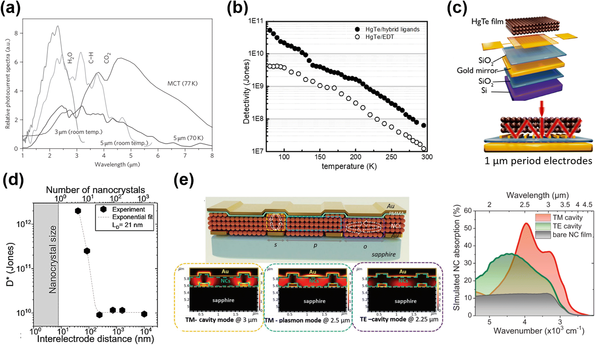 | ||
| Fig. 9 Inter-band absorption photoconductors. (a) Photocurrent spectra of 3 μm and 5 μm photoconductive devices. The spectrum recorded with a commercial nitrogen-cooled MCT detector is shown for comparison, but is not on the same y-axis scale. Reproduced from ref. 60 with permission from Springer Nature, copyright 2011. (b) Temperature-dependent detectivity of HgTe/hybrid and HgTe/EDT film-based photoconductors. Reproduced from ref. 101 with permission from American Chemical Society, copyright 2019. (c) The interdigitated electrodes were designed to induce a guided-mode resonance on the Si/SiO2 substrate with a gold reflecting mirror layer. Reproduced from ref. 89 with permission from American Chemical Society, copyright 2019. (d) Specific detectivity measured at 200 K as a function of electrode spacing. An exponential fit with a characteristic decay length of 21 nm is also plotted. Reproduced from ref. 119 with permission from Springer Nature, copyright 2021. (e) Schematic of the multi-resonant MWIR absorbing device with arrows indicating the regions where cavities are formed and the corresponding simulated absorption maps. Reproduced from ref. 120 with permission from Wiley-VCH, copyright 2022. | ||
As the photoconductive gain G ∝ τt·μ, high charge hopping mobility in the QD film is essential for a high photoconductive gain, so as to increase the responsivity. A series of ligands and ligand exchange methods were developed to optimize the film conductivity for photodetection applications, with the process detail being described in section 3.2. Using the inorganic ligand As2S3 to passivate the HgTe QDs via solid film ligand exchange, the charge mobility of the QD film was improved to μ ∼ 10−2 cm2 V−1 s−1, and a responsivity of ∼0.2 A/W and a detectivity >1010 Jones were reported at 230 K in 3.5 μm cut-off photoconductor samples.86 With optimization of the synthesis of non-aggregated HgTe QDs and solution phase ligand exchange with HgCl2 based hybrid ligands, the as-deposited QD films with band-like transport and high mobility result in a significant optimization in the photo-sensing ability.101,109 Photoconductive devices with hybrid ligands, although with half-thinner QD film thickness, achieved a 10-fold higher detectivity than that of devices treated with EDT, and reported a detectivity of 5.4 × 10¹⁰ Jones at 80 K with a cut-off wavelength of 4.8 μm (Fig. 9b).
The photo-sensing ability can also be enhanced by adding photonic structures to optimize the light absorption. For instance, by incorporation of a plasmonic optical nano-antenna array patterned between the interdigital electrodes, the photocurrent of a HgTe QD photoconductor was three-fold enhanced in the MWIR range.121 Chu et al. designed a photoconductor with a back-reflecting mirror and an optically designed interdigitated electrode to induce a guide-mode resonance (GMR) (Fig. 9c).89 In the ∼2.5 μm range, the responsivity of a device with a narrow electrode (∼1 μm gap) was enhanced by a factor of 1000, compared to the normal devices (with 30 μm gaps). The compact interdigital electrode also functioned as a diffraction grating that could be used to couple the IR light to the guided modes in the QD film to facilitate absorption. They further observed that the detectivity of the HgTe QD photoconductor could be orders of magnitude enhanced when reducing the channel gap to the charge diffusion length (equivalent to 5–10 nanocrystal diameters), as shown in Fig. 9d.119 The channel size reduction not only reduced the charge transit time, but also facilitated the delocalized charge transport at short distances, both factors boosting the photoconductive gain. With a set of nano-trench electrodes with a 40 nm-long nanogap, a detectivity of 1012 Jones at 2.5 μm under 1 V bias at 200 K was reported. Recently, a multi-resonant photonic sensor in the SWIR–MWIR range was demonstrated with the QD film coupled with a bottom grating formed by interdigitated electrodes for photocurrent collection, and a top metallic layer, as shown in Fig. 9e.120 With bottom illumination, a transverse magnetic (TM)-excited cavity mode between the top and bottom metal stripes, and a TM-excited surface plasmon mode at the QD/metallic layer interface and a transverse electric (TE)-excited resonance over the slit region were all obtained, resulting in a broadband enhancement of light absorption from 2 to 4 μm compared to bare QD films and a high responsivity of >0.7 A W−1 measured under 980 °C blackbody radiation. Similar photonic structures illustrated the potential of the QD film as a light modulator with a bias-tuneable spectral response,122,123 which originated in the inhomogeneous absorption in the QD film and the bias-dependent charge diffusion length.
Besides the spectral response and sensitivity, the temporal response is also an essential figure of merit to evaluate the operating bandwidth of a photodetector. Chen et al. reported a spray-deposited photoconductor in the SWIR range with TG ligand capped aqueous HgTe QDs with a 3 dB bandwidth of up to 1 MHz.84 They revealed that the response speed and responsivity of HgTe QD photoconductors are highly dependent on the illumination level and evaluated the energy depths of the trap states. In the MWIR range, a fast response with 100 ns decay time was observed in a ∼400 nm thick HgTe QD film capped with DDT ligands,83 and a 100 kHz 3 dB bandwidth was reported in the dots capped with As2S3 ligands.86 Compared to PbS QDs operating in the same SWIR range, the 3 dB bandwidth of the HgTe QD photoconductor was normally found to be larger.100 However, because of the structural characteristics, the temporal response of HgTe QD photoconductors is generally slower than that of photodiodes fabricated with the same dots,124 especially when used in weak light photodetection.
Although the HgTe QDs achieved several successes in IR detection, they are sensitive to the oxidation of Te.6,86 The self-n type doped properties of other Hg chalcogenide QDs may show an advance in ambient stability.6,73 Moreover, due to the sparse density of states in the conduction band, intra-band photodetection shows a narrow-band photoresponse with suppressed Auger recombination,70 which is attractive in photodetection applications. The investigations of intra-band photodetectors mainly focused on HgSe QDs with efforts in extending the spectral response range, optimizing the sensitivity and response speed. In 2014, Deng et al. first reported the photoconductance of monodisperse HgSe QDs with intra-band absorption in the 3–5 μm range.67 As the dark current was minimized when the 1Se state was fully doped with the 1Pe state being empty, the detectivity was optimized with the doping set at two electrons per dots. Fig. 10a shows the narrow-band spectral photo-response matching well with the intra-band absorption centred at around 4 μm. The absorption edge of a HgSe QD film was blue-shifted at low temperatures, which is in contrast to the behaviour of the inter-band absorption of HgTe QDs shown in Fig. 9a. Lhuillier et al. synthesized n-doped HgSe QDs with size continuously tuned between 5 and 40 nm, and extended the intra-band absorption up to 20 μm (Fig. 10b).6 Upon ligand exchange with As2S3, up to 100 cm2 V−1 s−1 electron mobility was observed in the solid film, and they reported a detectivity of around 108 Jones at RT in the MWIR range but with a very poor 3 dB bandwidth (∼40 Hz), as shown in Fig. 10c. Then, they synthesized nanocrystals of HgSe/HgTe core–shell type II heterostructures, and observed that the corresponding photoconductive devices had lower dark current, higher detectivity, and a slightly faster response speed (∼1 kHz) compared to the HgSe QD only devices (Fig. 10d).125 With devices deposited from a mixture of HgSe and HgTe QDs, a similar phenomenon was observed, which was attributed to the ultrafast charge transfer between the 1Se state of HgTe QDs and the 1Pe state of HgSe QDs.126 The narrow intra-band absorption can also be optimized using photonic structures, such as the GMR structure shown in Fig. 9c126 and plasmonic structures,97 by adjusting the photonic enhancement peak matching with the absorption peak.
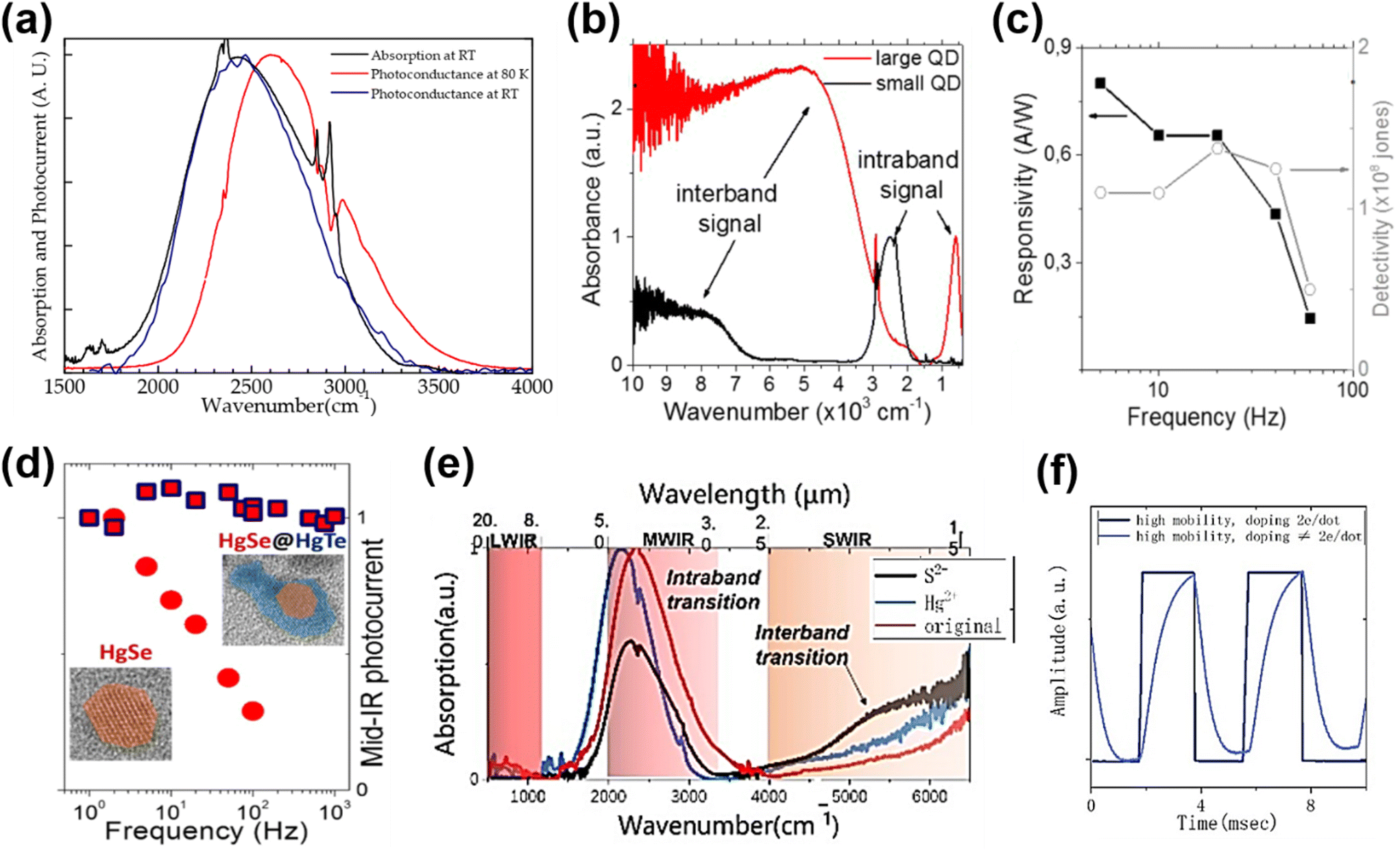 | ||
| Fig. 10 Intra-band absorption photoconductors. (a) Normalized absorption and photocurrent spectra of a HgSe QD film at RT. The photocurrent spectrum at 80 K exhibits a blue shift of 170 cm−1. Reproduced from ref. 67 with permission from American Chemical Society, copyright 2014. (b) Inter-band and intra-band absorbance spectra of small and large HgSe QDs, respectively. (c) Photoresponse and detectivity of a HgSe QD photoconductor with As2S3 ligands, as a function of operating frequency at RT. (b and c) Are reproduced from ref. 6 with permission from American Chemical Society, copyright 2016. (d) Normalized photocurrents of the HgSe QD and the HgSe/HgTe heterostructure QD photoconductors as a function of operating frequency. Reproduced from ref. 125 with permission from American Chemical Society, copyright 2018. (e) Absorption spectra of HgSe QDs with and without additional salts in ligand exchange. (f) Response speed of a HgSe intra-band QD photoconductor with different doping levels at 80 K. (e and f) Are reproduced from ref. 127 with permission from American Chemical Society, copyright 2022. | ||
Recently, a mixed-phase ligand exchange method combining liquid and solid phase treatments was developed to obtain a high mobility HgSe QD solid, and realize controllable doping from the 1Se to 1Pe state by adding different salts.127Fig. 10e and f show that the inter-band and intra-band absorption can be tuned by p-type ((NH4)2S) and n-type (HgCl2) doping, and that the response speed of the corresponding devices is highly dependent on the doping level of the QDs. The responsivity of the HgSe QD photodetectors was also varied with ligands adopted in a solid-phase treatment, showing that the best performance was obtained with the NH4SCN ligand.128
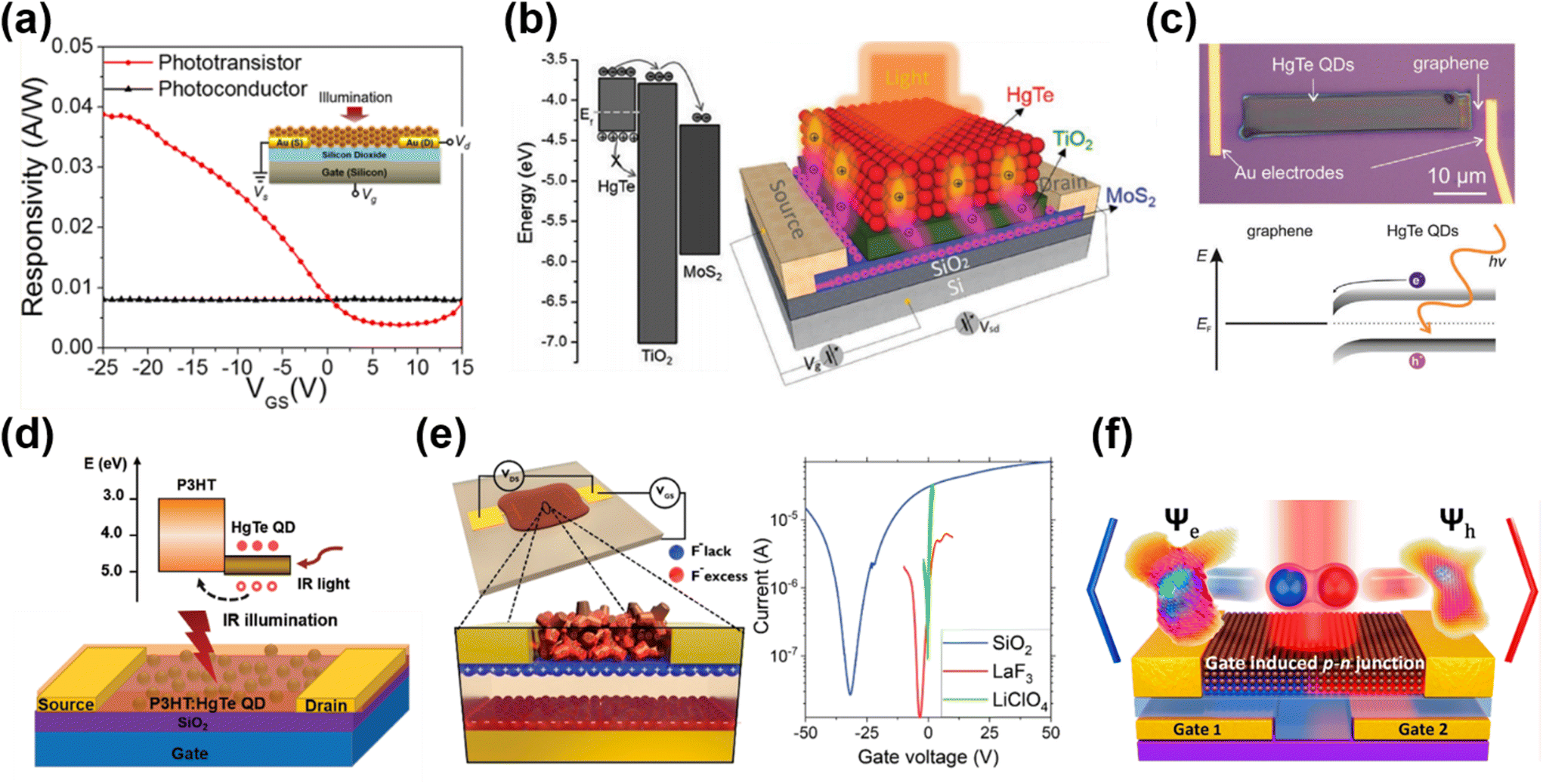 | ||
| Fig. 11 Different device architectures of phototransistors. (a) Device structure and the gate-voltage-tuned responsivity of a phototransistor in comparison with floating-gate operation. Reproduced from ref. 2 with permission from American Chemical Society, copyright 2017. (b) Schematic of a MoS2/TiO2/HgTe QD hybrid phototransistor and the band alignment. Reproduced from ref. 129 with permission from Wiley-VCH, copyright 2017. (c) Band alignment and an optical image of a graphene/HgTe QD phototransistor deposited with an electrohydrodynamic nano-printing technique. Reproduced from ref. 130 with permission from Wiley-VCH, copyright 2021. (d) Schematic of a P3HT/HgTe QD hybrid phototransistor and the corresponding band alignment. Reproduced from ref. 133 with permission from Wiley-VCH, copyright 2020. (e) Schematic of a HgTe QD phototransistor on LaF3 ionic glass with Vgs > 0 and the typical transfer curves of HgTe QDs with dielectric (SiO2), ionic glass (LaF3) and electrolyte (LiClO4) gating. Reproduced from ref. 134 with permission from American Chemical Society, copyright 2019. (f) A p–n junction induced in a dual-gate device with Al2O3 as a high-k dielectric. Reproduced from ref. 135 with permission from American Chemical Society, copyright 2021. | ||
The planar geometry of phototransistors offers device structure flexibility for narrow-bandgap QDs for heterojunction stacking with other materials. Huo et al. proposed a MoS2–HgTe QD hybrid phototransistor by depositing a QD layer on a TiO2 encapsulated MoS2 transistor (Fig. 11b).129 With a TiO2 buffer layer used to form a p–n junction with the HgTe QDs, the photo-generated electrons could be efficiently transferred into the high-mobility MoS2 channel and the holes were trapped in the QD layer. This structure boosted the photoconductive gain and suppressed the noise current in the depletion regime, and they reported a record responsivity of 106 A W−1 and a detectivity of 1012 Jones at 2 μm at RT. Similar heterojunction stacking to both exploit the high mobility of 2D materials and the IR absorption of the QDs was demonstrated in a nano-printed HgTe QD/graphene heterojunction phototransistor with high responsivity and up to 3 μm spectral response (Fig. 11c).130 The graphene/HgTe QD heterojunction was also adopted in four-terminal planar devices131 and a vertical geometry phototransistor design132 to realize a gate-voltage tuned photovoltaic response. In 2020, a bulk-heterojunction nanocomposite, blending a semiconducting polymer poly(3-hexylthiophene) (P3HT) and HgTe QDs, was demonstrated with a phototransistor structure for SWIR detection (Fig. 11d).133 By shifting the transport path of the photo-generated charges into the P3HT matrix, and by the carefully arranged chemical grafting between the P3HT and HgTe QDs to realize good surface passivation, the noise level of the device was reduced to reach a RT detectivity of 1011 Jones up to 2.3 μm with a response decay time of <1.5 μs. This device shows advances in all-solution processability for large-scale production with a performance comparable to commercial InGaAs photodetectors operating in the same wavelength range.
Besides the traditional Si/SiO2 wafer design for QD FETs, Gréboval et al. explored the use of LaF3 ionic glass as a high-capacitance substrate for QD phototransistor demonstrations.134 As shown in Fig. 11e, the capacitance of the ionic glass is associated with the dielectric capacitance through the substrate and the displacement of F− vacancies with gate bias. A phototransistor could be realized by depositing the HgTe QD film on the ionic glass with pre-patterned metal electrodes, with lower gate voltage threshold and good tunability in sensitivity and temporal response. By replacing the source–drain metallic electrodes with graphene electrodes, this structure demonstrated a tunable p- or n-type doping of the HgTe QD film.136 A planar p–n junction was created to facilitate charge dissociation, so as to optimize the photocurrent and suppress the dark current. A planar p–n junction was also created with a dual-gate structure by applying voltages on different gates to select the doping type in the intrinsic QD film for charge separation mechanism investigation (Fig. 11f),135 or to realize a fast response time of a few nanoseconds.137 For intra-band absorption, HgSe QD/ZnO thin-film transistors with MIR responses were also explored.94
The first Hg chalcogenide QD photodiode was constructed with a heterojunction formed between n-type ZnO nanowires and p-type HgTe QD films in 2009.138 With their IR absorption properties, the HgTe QD photodiodes were initially explored as photovoltaic cells, with device structures consisting of QD sensitized mesoporous TiO2,139 and inverted solar cells with the nanocomposites of HgTe QDs and a polymer.140 In 2014, addressing the poor absorption of HgTe QD films, Chen et al. reported a plasmonically-enhanced photodiode with a structure composed of ITO/ZnO/HgTe QDs/MoO3/Au layers and calibrated its photosensing ability up to 1.4 μm (Fig. 12a).141 They transferred a panel of normal random distributed Au nanorods into a controllable depth of the ETL ZnO layer, and observed an ∼240% increment of the short-circuit current compared to the reference (Au nanorod-free) structure, without affecting the dark current and response speed. Jagtap et al. focused on the photosensing ability in the 1.7–2.5 μm range, and designed a unipolar barrier in the HgTe QD photodiode structure in 2018.88 They inserted a p-type HgTe QD layer with a larger bandgap (∼0.72 eV) between the MoO3 HTL and the light-absorbing ambipolar QD layer (∼0.5 eV bandgap) operated as an electron blocking layer, so as to suppress the dark current. Then, this unipolar diode was optimized by taking the large bandgap QDs as the HTL and getting rid of the TiO2 layer with its rather poor band alignment for electron extraction (Fig. 12b).108 With the QDs prepared with solution phase hybrid ligand exchange in a DMF ink for deposition, up to 600 nm QD film thickness with high carrier mobility was realized, and the authors reported a detectivity of 3 × 10⁹ Jones at RT.
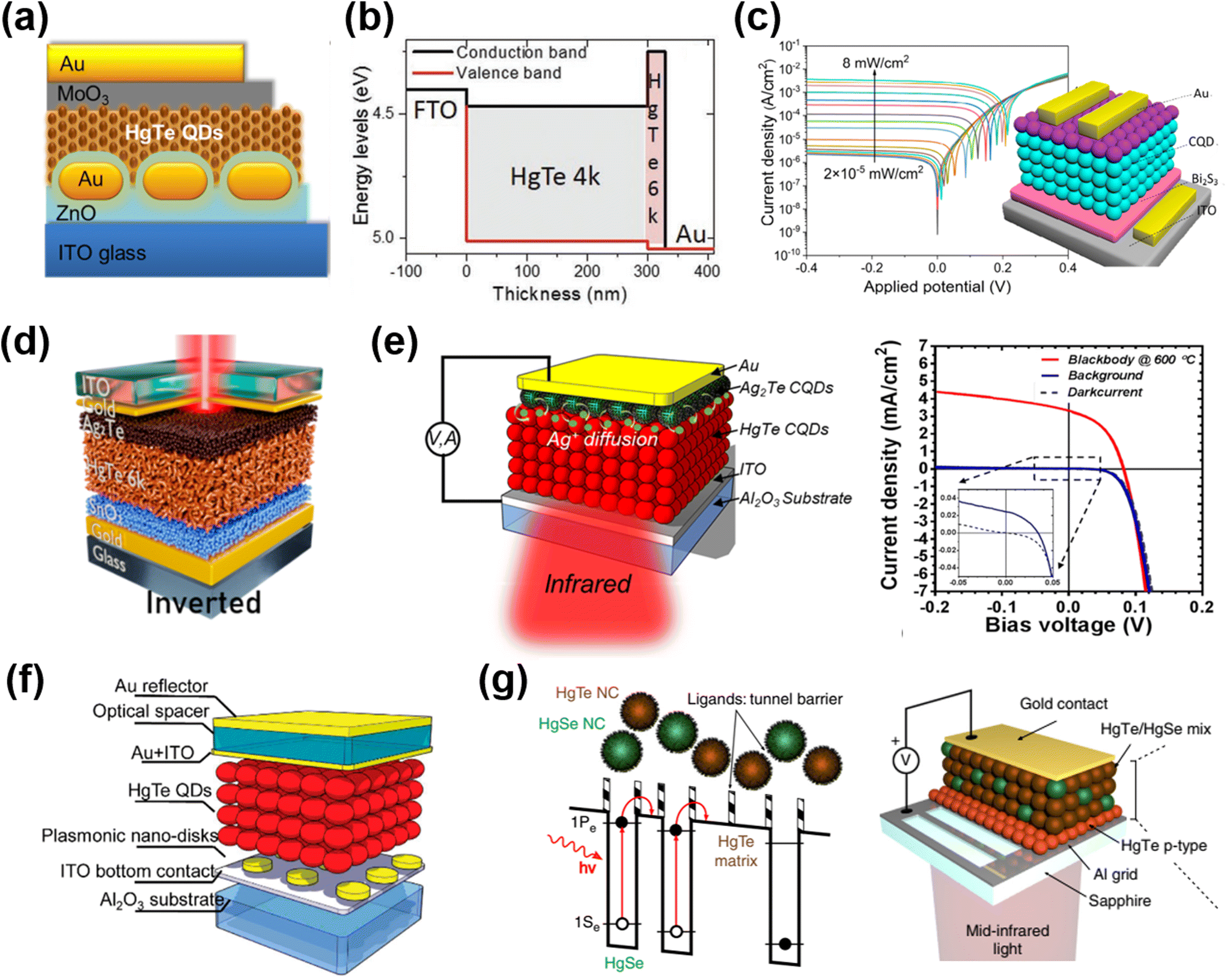 | ||
| Fig. 12 Different device architectures of photodiodes. (a) Schematic of a HgTe QD/ZnO photodiode with Au nanorods embedded in the ZnO layer. Reproduced from ref. 141 with permission from American Chemical Society, copyright 2014. (b) Band alignment of a unipolar photodiode stack of HgTe QD layers with an excitonic peak at 4000 cm−1 (4k, ∼0.5 eV bandgap) and 6000 cm−1 (6k, ∼0.72 eV bandgap). Reproduced from ref. 108 with permission from Wiley-VCH, copyright 2019. (c) Schematic of a Bi2S3/HgTe QD/Ag2Te QD photodiode and its current–voltage characteristics under 1550 nm illumination. Reproduced from ref. 145 with permission from American Chemical Society, copyright 2022. (d) Schematic of the reverse biased diode based on the doped SnO2/HgTe QD/Ag2Te QD stack. Reproduced from ref. 146 with permission from American Chemical Society, copyright 2022. (e) Schematic of the MIR HgTe QD/Ag2Te QD photodiode and the current–voltage characteristics in the dark and under background radiation and 600 °C blackbody radiation when operated at 85 K. Reproduced from ref. 148 with permission from American Chemical Society, copyright 2018. (f) Illustration of the MIR HgTe QD photodiode with an interference structure and a plasmonic disk array. Reproduced from ref. 149 with permission from American Chemical Society, copyright 2018. (g) Scheme of a random distributed mixture of HgSe QDs (as an IR absorber) and HgTe QDs (as a barrier) to mimic the energy landscape of the quantum well/dot IR photodetectors and the corresponding device structure. Reproduced from ref. 150 with permission from Springer Nature, copyright 2019. | ||
Inspired by the diode structures in the MWIR range, Tang et al. reported flexible QD photovoltaic detectors in the SWIR range based on a p–i–n junction over the HgTe QD film, which was simultaneously p-type doped by Ag2Te QDs and n-type doped by Bi2Se3 QDs.142 With the light absorption being enhanced by a Fabry–Perot (FP) resonance across the devices, a RT detectivity of up to 7.5 × 10¹⁰ Jones at 2.2 μm was reported. Ackerman et al. optimized the HgTe QD/Ag2Te QD photodiode in the SWIR range by performing a HgCl2 treatment after each layer EDT/HCl ligand exchange of HgTe QDs, showing that the shunt resistance could be significantly improved to reduce the dark current. A detectivity of 1011 Jones was reported at 2.2 μm at RT, which is comparable to the performance of epitaxial InGaAs.143 The photonic grating structures were also designed to optimize the light absorption and open-circuit voltage of the photodiode in the SWIR range.144
Recently, Yang et al. fabricated a p–i–n photodiode of thermally evaporated Bi2Se3 thin film/HgTe QD/Ag2Te QD stacking, as shown in Fig. 12c.145 This device was fabricated with monodisperse HgTe QDs with sharp absorption edges, which are produced with a ligand-engineering growth approach. A rectification ratio of up to 2000 and a record low dark current of 2.3 × 10⁻⁶ A cm−2 under −0.4 V reverse bias were achieved, resulting in a high LDR of over 112 dB at 1.55 μm. Other alternative ETLs were also explored with doped SnO2146 and CdSe QD147 layers, with the optimal band alignment of HgTe QDs to improve the electron extraction and block the hole current. An inverted diode structure was also demonstrated with a stack of doped-SnO2/HgTe QDs/Ag2Te QDs, which was compatible with ROIC integration, with a top illumination scheme (Fig. 12d). Moreover, the SnO2 layer benefited the electron injection under forward bias and this was the first reported instance of a HgTe QD photodiode with both photo-sensing and electroluminescence (EL) abilities.
In the MWIR range, photodiode structure optimization is more challenging and high detectivity can only be achieved with cryogenic cooling. Guyot-Sionnest et al. reported the first HgTe QD photodiode with MWIR responses in 2015.151 The device was a Schottky diode formed by capping the HgTe QD film between a NiCr semi-transparent conducting electrode and a layer of silver paint. They reported a detectivity of >1010 Jones in the samples with 3–5 μm absorption in the range below 140 K. BLIP was achieved at 90 K in the detector with a cut-off wavelength of 5.25 μm. In 2018, Ackerman et al. adopted an ITO electrode (with better IR transmission) and designed a HgTe QD/Ag2Te QD PN junction diode with HgCl2 treatment used to ensure reliable rectification (Fig. 12e).148 These devices exhibited BLIP up to 140 K, as per the contrast between the dark and background radiation currents shown in the current–voltage curves. The MWIR absorption of this device could be further enhanced by the integration of a constructive interference cavity and plasmonic structures, as shown in Fig. 12f.149 The photonic structures boosted the light absorption of the photodiode in the 3–5 μm range, and they reported a detectivity of up to 4 × 10¹¹ Jones at 85 K. MWIR photodetection can also be realized with a unipolar intra-band photodiode with a mixture of HgTe and HgSe QDs to mimic inorganic quantum well/quantum dot IR photodetectors relying on inter-sub-band transitions; the operating mechanism and the device structure are shown schematically in Fig. 12g.150 By choosing the size of the HgTe QDs to tune the barrier height and width, the photo-generated carriers in the HgSe QDs could be efficiently extracted with suppressed thermally activated noise. A detectivity of 1.5 × 10⁹ Jones was reported at 80 K with a sub-500 ns response time at around 4 μm. Recently, with precise doping control of HgTe QDs with surface dipoles introduced by the HgCl2 or (NH4)2S salt, a PIN gradient homojunction photodiode was demonstrated with optimized open-circuit-voltage and suppressed thermal noise.152 A record high detectivity of 2.7 × 10¹¹ Jones at 80 K (above 1011 Jones up to 280 K) was reported at 4.2 μm, showing a QD-based high-operating-temperature MWIR photodetector with a performance beyond that of epitaxially-grown inorganic photodetectors.
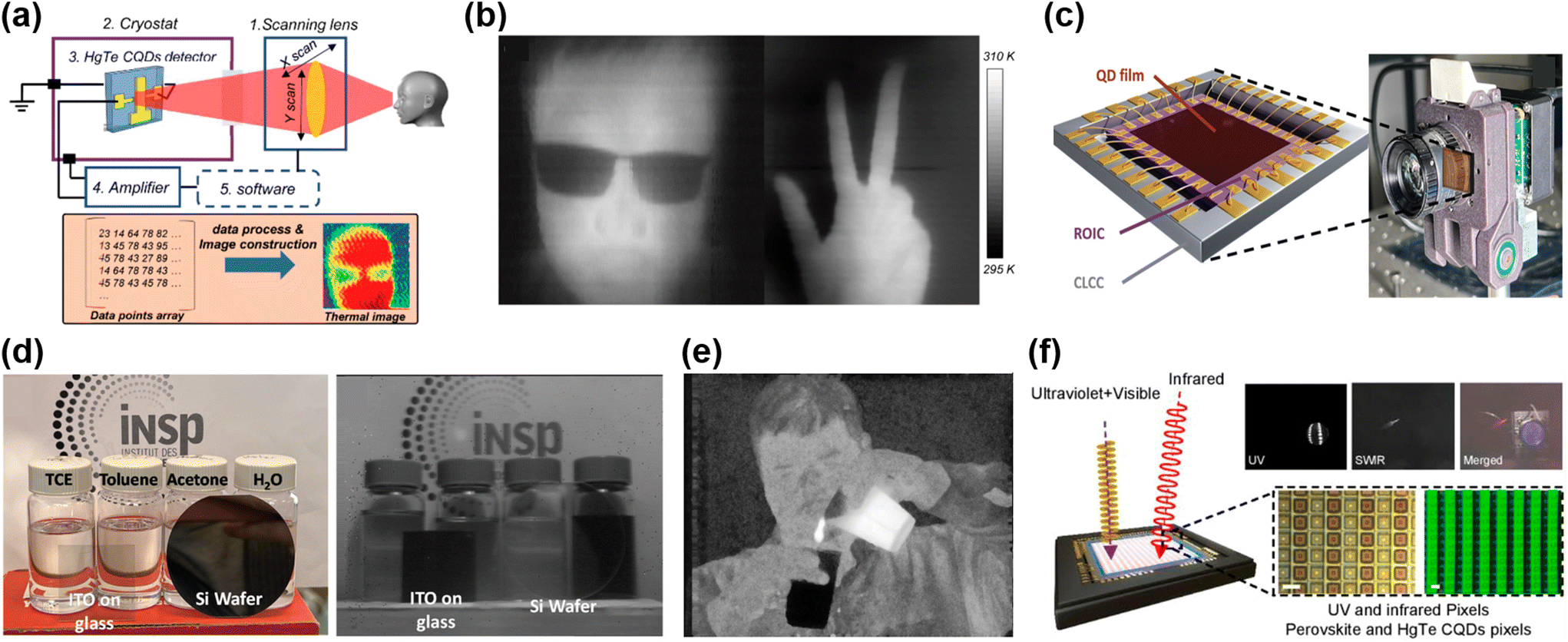 | ||
| Fig. 13 Imaging demonstrations. (a) Illustration of a single-pixel scanning system of a HgTe QD imaging detector and (b) the thermal image captured by this system with the HgTe QD MWIR detector operated at 90 K. (a and b) Are reproduced from ref. 149 with permission from American Chemical Society, copyright 2018. (c) Scheme of a HgTe QD film deposited on the ROIC in the ceramic lead-less chip carrier (CLCC) as the imaging array in a camera system. (d) Visible and SWIR pictures (taken by a HgTe QD based FPA) of four vials containing different chemical solvents. An ITO covered glass slide and a two-inch diameter silicon wafer are placed in front of the vials. (c and d) Are reproduced from ref. 155 with permission from the Royal Society of Chemistry, copyright 2022. (e) An image obtained by a HgTe QD coated FPA in the MWIR range showing a person pouring hot water into cold water. Reproduced from ref. 156 with permission from the Society of Photo-Optical Instrumentation Engineers, copyright 2016. (f) Schematic configuration of a multispectral CMOS-compatible imager with photolithographically patterned UV-enhanced visible pixels and SWIR pixels. The insets are the merged multispectral image captured in the UV (blue), visible light (grayscale), and SWIR (red) channels. Reproduced from ref. 157 with permission from American Chemical Society, copyright 2022. | ||
For commercial applications, mechanical scanning and image construction with a single-pixel detector are far of lower quality than required to fulfil the specifications for fast frame rate and high-resolution imaging nowadays. Solution processable QDs with size-tuneable IR absorption and low fabrication cost are considered as promising candidates to be applied in 4th generation IR detection systems with complex focal plane arrays (FPAs) and three-dimensional ROICs for high-resolution imaging or machine vision systems.158 Most investigations to integrate Hg chalcogenide QDs with FPAs are still in their early stages, with simple demonstrations to capture images by coating the Hg chalcogenide QD films onto commercially-available ROIC substrates.155,156,159 Unlike epitaxially-grown IR sensing semiconductors that are limited by the size of the indium bump array used to connect with the silicon ROIC, the HgTe QDs can directly and intimately integrate with the FPA with a very small pixel size for high resolution imaging. Fig. 13c illustrates a HgTe QD based FPA chip structure operated in the SWIR range, with a 640 × 512 pixel array and a pitch size of 15 μm, to be plugged into a camera system.155 A full frame SWIR image could be captured at up to 200 frames per second (fps), with a large contrast to the visible image of the same scene (Fig. 13d), showing promise for applications in object demarcation and chemical discrimination. Fig. 13e provides a MWIR image captured by a HgTe QD coated FPA, which was fabricated on a 320 × 256 pixel ROIC with a pitch size of 30 μm, with the ability to record the images with a NEDT of 102 mK at 100 K operation temperature.156 For small pixel size, the cross-talk and optical coupling between different pixels should be considered for further optimization of the imaging resolution and quality, which may require the use of lithography to define the pixel areas in the QD film.11 To enhance the sustainability of the soft Hg chalcogenide QD film, Martinez et al. designed a concave pixel unit to hold the HgTe QDs, realizing a self-fabricated FPA with a 10 × 10 pixel matrix having a high survival rate of pixels (pixel yield), good homogeneity and low spatial noise.100,108 Zhang et al. developed a spray-stencil lithography process for array demonstration with a defined spatial distribution of the HgTe QD film features, while the pixel size was limited by the shadow mask feature sizes.160 Recently, with ultraviolet (UV)-activated ligands to interlock with the as-synthesized HgTe QDs and perovskite QDs, a multi-spectral broadband imager with UV-enhanced visible pixels and SWIR sensitive pixels patterned with layer-by-layer optical lithography was constructed on a custom-designed CMOS based ROIC panel, as shown in Fig. 13f.157 A 320 × 256 array with a pixel pitch of 30 μm was fabricated, which demonstrated the merging of images with frames captured in the UV, visible and SWIR channels simultaneously.
Spectral or polarization selectivity. Multispectral sensing means a device can simultaneously detect a photo-response in two or more wavelength ranges. Multispectral sensing can be realized by planar patterning the QD films with dots having different absorption edges at specific locations across the electrode array on one single substrate,96,98,160 or by vertically stacking two diodes with different spectral responses, such as a HgTe QD/graphene/silicon dual-channel detector for both SWIR and visible signal collection (Fig. 14a).161 The vertically stacked diode structure was also employed to realize dual-channel, polarization-sensitive detection, with the first diode providing unpolarized information and the second diode being sensitive to light polarization.162
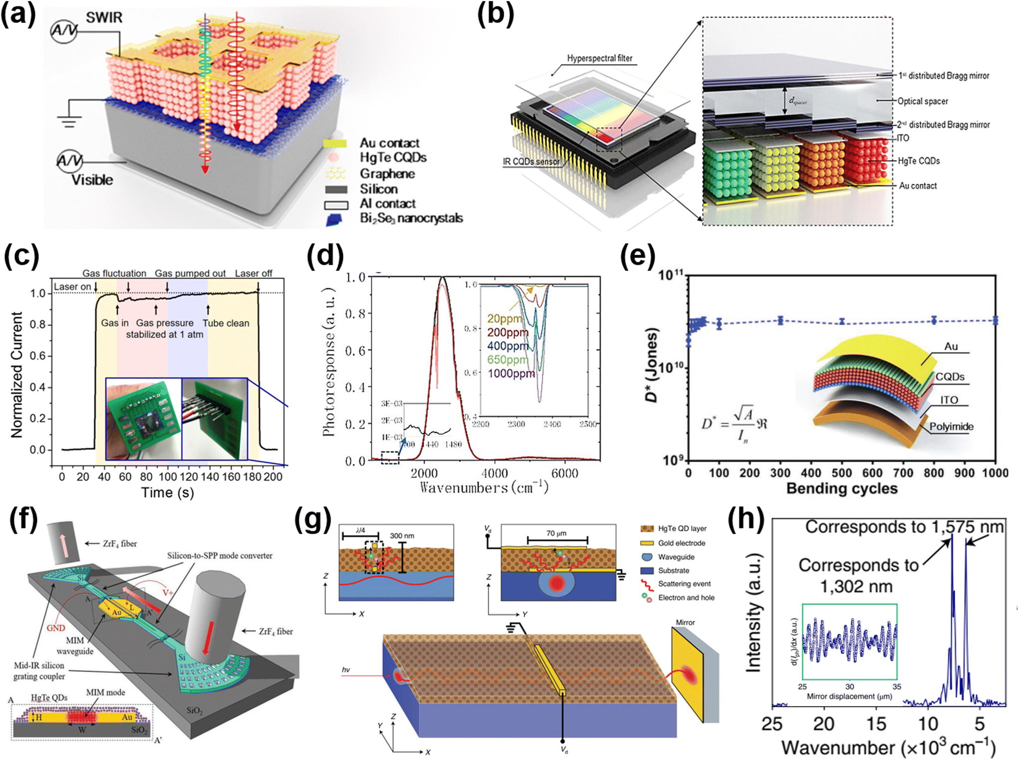 | ||
| Fig. 14 Demonstration of diverse applications. (a) Schematic of a HgTe QD/graphene/silicon SWIR/visible dual-channel detector. Reproduced from ref. 161 with permission from American Chemical Society, copyright 2020. (b) Schematic of the single pixel hyperspectral sensor consisting of HgTe QD layers and the hyperspectral filter arrays. Reproduced from ref. 154 with permission from Wiley-VCH, copyright 2019. (c) Photocurrent response of a RT-operated HgTe QD phototransistor in a practical CO gas sensing measurement. Reproduced from ref. 2 with permission from American Chemical Society, copyright 2017. (d) Photo-response spectra of a HgSe QD photoconductor with different CO2 concentrations. Reproduced from ref. 127 with permission from American Chemical Society, copyright 2022. (e) Schematic of a flexible HgTe QD photodiode and the detectivity during concave bending cycles. Reproduced from ref. 142 with permission from Wiley-VCH, copyright 2019. (f) Schematic of an on-chip integrated photodetector based on a plasmonic-silicon hybrid waveguide system with the QDs covering the metal–insulator–metal (MIM) waveguide (cross-section AA′ in the inset). Reproduced from ref. 95 with permission from Wiley-VCH, copyright 2019. (g) Schematic of a waveguide spectrometer with an integrated photoconductor and the respective cross-sections. (h) Input light source spectrum retrieved with fast Fourier transformation of the photo-signal as a function of mirror displacement shown in the inset. (g and h) Are reproduced from ref. 163 with permission from Springer Nature, copyright 2023. | ||
Multispectral sensing has been demonstrated in a series of innovative applications. In 2019, a dual-band n–p–n photodiode was reported with two stacked HgTe QD layers with photo-responses respectively in the SWIR and MWIR ranges.153 When the two HgTe QD layers were separated by a p-type doping layer, two rectifying junctions were formed across the diode, providing a bias-switchable spectral response in different IR bands. With an alternating current bias operation, this device could capture the SWIR and MWIR signals of the targets at the same time, to remotely evaluate the image object's temperature (e.g. a soldering iron and a heat gun were imaged with a good signal ratio). A hyperspectral sensor (a sensor that can obtain full spectral information within a single detection unit) with 64 channel spectral resolution in the SWIR range was demonstrated by stacking the HgTe QD photodiodes on top of a distributed Bragg mirror (DBR) filter array (Fig. 14b).154 The SWIR hyperspectral sensor with a full-wavelength half maximum (FWHM) of a sensing band of 40 ± 7 cm−1 was operated as a single pixel spectrometer to record the water absorption spectra, or to capture images with spectral information in each pixel for optical information analysis.
Gas sensing. As the vibration wavelengths of gas molecules are in the IR range, the Hg chalcogenide QD IR photodetectors are promising candidates for gas detection and industrial process monitoring applications, with the advantages of low fabrication cost and high (rather than cryogenic) temperature operation. As shown in Fig. 14c, a RT-operated HgTe QD phototransistor was applied in a practical CO gas detection system, which precisely recorded the light absorption variation due to CO gas being pumped in and out of a 10 cm long glass absorption cell tube with continuous 2327 nm illumination, and the absorption coefficient was evaluated.2 Gas detection was also demonstrated with a HgSe QD photoconductor at an intra-band absorption peak in the MWIR range with cryogenic cooling, to evaluate CO2 gas concentration as low as 20 ppm (Fig. 14d) in another demonstration.127
Flexible devices. Flexible photodetectors have been demonstrated in both photoconductor98 and photodiode142,160 schemes. As shown in Fig. 14e, the flexible HgTe QD photodiode had excellent mechanical flexibility and maintained a high detectivity after a repeated thousand times bending test. The SWIR image could be captured under different bending radii, showing a potential route to IR electronic ‘eyes’ i.e., devices with a curved imaging plane. An IR free-space signal optical communication system was also demonstrated with this device acting as a signal receiver to a coded light source.
On-chip integration. In addition to photodetection in free-space, an on-chip integrated photodetector is a promising component in photonic integrated circuits and optical system miniaturization. Zhu et al. designed a plasmonic-silicon hybrid waveguide system loaded with HgTe QDs, and demonstrated on-chip photodetection with the guided wave at wavelengths of ∼1600 nm
164 and ∼2300 nm,95 respectively. Fig. 14f shows the device with the input/output silicon waveguide grating couplers and the metal–insulator–metal (MIM) plasmonic waveguide. The MIM waveguide functioned both as photoconductive electrodes and the plasmonic waveguide to concentrate the IR absorption of the slit-loaded QDs. This device was fabricated with a silicon-on-insulator platform, with a small footprint of 15 μm × 0.35 μm, which is highly compatible with silicon photonic circuit designs. Recently, a compact Fourier-transform waveguide spectrometer was demonstrated with a HgTe QD based integrated photodetector.163 As shown in Fig. 14g, a buried and leaky optical waveguide was coated with a thin photoactive QD layer, with sub-wavelength-sized gold electrodes to both function as a scattering centre and to collect the photoconductive current. A stationary wave was formed within the waveguide with the mirror reflection of the input optical beam, and the input spectrum could be retrieved with fast Fourier transformation of the photo-signal as a function of mirror displacement, which was recorded by the integrated photodetector (Fig. 14h). This spectrometer exhibited a large wavelength sensing range from 400 nm to 2 μm, and an active spectrometer volume below 100 μm × 100 μm × 100 μm.
The comprehensive comparisons in material, structure and performance of the representative Hg chalcogenide CQD based IR photodetectors are summarized in Table 2.
| Year | Type | Active material (structure/features) | Ligand exchange (in the solid/liquid phase) | Spectral range | Responsivitya | Detectivitya | Signal bandwidth or response time | Ref. |
|---|---|---|---|---|---|---|---|---|
| a Unless otherwise noted, the data are recorded at room temperature (from 295 K to 300 K). PC: photoconductor; PT: phototransistor; PD: photodiode; DDT: dodecanethiol; EDT: ethanedithiol; MPA: mercaptopropionic acid; TG: thioglycerol; β-ME: β-mercaptoethanol; ONAs: optical nano-antenna; GMR: guide-mode resonance. | ||||||||
| Inter-band absorption | ||||||||
| 2007 | PC | HgTe QDs | DDT (no exchange) | 1–3 μm | Up to 4.4 A W−1@1.4 μm | 3.2 × 10¹⁰ Jones@1.4 μm | — | 116 |
| 2011 | PC | HgTe QDs | DDT (no exchange) | Up to 5 μm | 0.25 A W−1 | 2 × 10⁹ Jones@130 K | ∼4 kHz | 60 |
| 2013 | PC | HgTe QDs | As2S3 (solid) | Up to 3.5 μm | >0.1@3.5 μm@230 K | 3.5 × 10¹⁰ Jones@3.5 μm@230 K | ∼100 kHz | 86 |
| 2014 | PC | HgTe QDs | EDT/HCl (solid) | Up to 12 μm | 0.3 mA W−1@80 K | 6.5 × 10⁶ Jones@80 K | <5 μs | 5 |
| 2014 | PC | HgTe QDs | TG (no exchange) | Up to 1.4 μm | 0.3 A W−1@1.1 μm | >1010 Jones@1.1 μm | ∼1 MHz | 84 |
| 2016 | PC | HgTe QDs (multispectral) | As2S3 (solid) | 2–10 μm | 0.1 A W−1@2 μm | 2 × 10⁷ Jones@2 μm | Rise 91.5 ms, fall 541.3 ms | 96 |
| 2017 | PC | HgTe QDs (plasmonic ONAs) | EDT/HCl (solid) | 3–5 μm | 0.19 A W−1@80 K | 1.52 × 10¹⁰ Jones@80 K | — | 121 |
| 2018 | PC | HgTe QDs (multispectral, flexible) | As2S3 (solid) | 2.3–4.3 μm | 0.9 A W−1 | 8 × 10⁹ Jones | Fall ∼1 ms | 98 |
| 2019 | PC | HgTe QDs (GMR) | EDT (solid) | Up to 2.6 μm | 1 A W−1 | >1010 Jones@200 K | 1 kHz | 89 |
| 2019 | PC | HgTe QDs (plasmonic waveguide) | MPA (solid) | 2.3 μm | 23 mA W−1@2.3 μm | 3.2 × 10⁶ Jones@2.3 μm | 10 kHz | 95 |
| 2019 | PC | HgTe QDs | HgCl2 based hybrid ligands (liquid) | Up to 4.8 μm | 0.23 A W−1@80 K | 5.4 × 10¹⁰ Jones@80 K | Rise 0.9 μs, fall 2 μs | 101 |
| 2021 | PC | HgTe QDs (nanotrench channel) | HgCl2 based hybrid ligands (liquid) | Up to 2.5 μm | 103 A W−1@200 K | 1012 Jones@200 K | 20 μs | 119 |
| 2022 | PC | HgTe QDs (multi-resonant sensor) | HgCl2 based hybrid ligands (liquid) | Up to 4 μm | >0.7 A W−1@80 K | 2 × 10¹⁰ Jones@80 K | 11 μs | 120 |
| 2022 | PC | HgTe QDs (bias-dependent response) | HgCl2 based hybrid ligands (liquid) | Up to 4 μm | 0.32 A W−1@80 K | 7 × 10¹⁰ Jones@80 K | 70 ns | 123 |
| 2022 | PC | HgTe QDs (integrated spectrometer) | EDT (solid) | Up to 2 μm | 0.6 A W−1 | 3 × 10⁹ Jones | — | 163 |
| 2022 | PC | HgTe QDs (multi-spectral CMOS imager) | EDT (solid) | Up to 2.5 μm | 0.25@2 μm | 1.5 × 10¹⁰ Jones | 1 μs | 157 |
| 2017 | PT | HgTe QDs | TG (no exchange) | Up to 2.2 μm | ∼0.4 A W−1 | ∼2 × 10¹⁰ Jones | 10 kHz | 2 |
| 2017 | PT | HgTe QD–MoS2 | EDT (solid) | Up to 2.1 μm | 106 A W−1@2 μm | 1012 Jones@2 μm | Fall < 4 ms | 129 |
| 2020 | PT | HgTe QD:P3HT blends |
EDT (solid) | Up to 2.5 μm | >1 A W−1 up to 2.25 μm | >1011 Jones up to 2.3 μm | Fall 1.5 μs | 133 |
| 2021 | PT | HgTe QD–graphene | EDT/HCl (solid) | Up to 3 μm | 150 A W−1@2.5 μm@80 K | 6 × 10⁸ Jones@2.5 μm@80 K | Rise 0.4 ms fall 0.7 ms | 130 |
| 2021 | PT | HgTe QDs (split gate p–n junction) | HgCl2 based hybrid ligands (liquid) | Up to 2.5 μm | 2.0 × 10⁻³ A W−1@250 K | — | Fall 3 ns | 137 |
| 2014 | PD | ZnO/HgTe QDs/MoO3 (plasmonic Au nanorods) | TG (no exchange) | Up to 1.4 μm | — | Up to 1.4 × 10¹⁰ Jones | ∼1 MHz | 141 |
| 2015 | PD | HgTe QDs/Ag (NiCr electrode) | EDT/HCl (solid) | Up to 5.2 μm | 86 mA W−1@90 K | 4.2 × 10¹⁰ Jones@90 K | Fall 0.7 μs@120 K | 151 |
| 2018 | PD | HgTe QDs/Ag2Te QDs | EDT/HCl (solid) | 3–5 μm | 1.3 A W−1@85 K | 3.3 × 10¹¹ Jones@85 K | Rise 0.3 μs fall 1 μs@85 K | 148 |
| 2018 | PD | HgTe QDs/Ag2Te QDs (plasmonic Au nanodisks) | EDT/HCl (solid) | 3–5 μm | 1.62 A W−1@4.5 μm@85 K | 4 × 10¹¹ Jones@85 K, 1010 Jones@220 K | <1 μs | 149 |
| 2018 | PD | HgTe QDs (HgTe QD barrier layer) | EDT (solid) | Up to 2.5 μm | 1 mA W−1 | 3 × 10⁸ Jones | >10 kHz | 88 |
| 2019 | PD | HgTe QDs (HgTe QD barrier layer) | HgCl2 based hybrid ligands (liquid) | Up to 2.5 μm | 20 mA W−1 | 3 × 10⁹ Jones | Fall 370 ns | 108 |
| 2019 | PD | Bi2S3 QDs/HgTe QDs/Ag2Te QDs (flexible) | EDT/HCl (solid) | Up to 2.5 μm | 0.22 A W−1 | 7.5 × 10¹⁰ Jones@2.2 μm | 1 MHz | 142 |
| 2019 | PD | Bi2S3 QDs/HgTe QDs/Ag2Te QDs (n–p–n dual-band) | EDT/HCl (solid) | SWIR and MWIR range | — | >1010 Jones for SWIR, for MWIR@150 K | 100 kHz | 153 |
| 2020 | PD | HgTe QDs/Ag2Te QDs | HgCl2 and EDT/HCl (solid) | 2–2.6 μm | ∼1 A W−1 | 1011 Jones@2.2 μm | Rise 450 ns fall 1.4 μs | 143 |
| 2019 | PD | Bi2S3 QDs/HgTe QDs/Ag2Te QDs (hyperspectral) | EDT/HCl (solid) | 1.5–2.1 μm | 0.2 A W−1 | Above 1010 Jones | Rise time 120 ns | 154 |
| 2021 | PD | HgTe QDs/Ag2Te QDs (2D Al grating) | HgCl2 based hybrid ligands (liquid) | Up to 2 μm | 0.2 A W−1 | 2 × 10¹⁰ Jones | Fall time 110 ns | 144 |
| EDT (solid) | ||||||||
| 2022 | PD | HgTe QDs/Ag2Te QDs (spray-stencil lithography) | EDT/HCl (solid) | Up to 5 μm | ∼0.3 A W−1@SWIR; ∼0.5 A W−1@MWIR@80 K | >1010 Jones (no T Infor) | Rise and fall time 6.4 μs | 160 |
| 2022 | PD | Bi2S3/HgTe QDs/Ag2Te QDs | HgCl2 and EDT/HCl (solid) | Up to 1.7 μm | 0.38 A W−1@1.55 μm | 3.9 × 10¹¹ Jones@1.55 μm | Rise 6.4 μs, fall 25.4 μs | 145 |
| 2022 | PD | SnO2/HgTe QDs/Ag2Te QDs | HgCl2 based hybrid ligands (liquid) | Up to 2 μm | 0.3 A W−1 | 5 × 10¹⁰ Jones | 300 ns | 146 |
| 2022 | PD | CdSe QDs/HgTe QDs/Ag2Te QDs | HgCl2 based hybrid ligands (liquid) | Up to 2 μm | 0.8 A W−1 | 9 × 10¹⁰ Jones | 170 ns | 147 |
| 2023 | PD | HgTe QD PIN homojunction | β-ME with HgCl2 or (NH4)2S (liquid) | Up to 4.2 μm | 2.6 A W−1@80 K | 2.7 × 10¹¹ Jones@80 K | 500 Hz | 152 |
| EDT/HCl (solid) | 2.0 A W−1@200 K | Above 1011 Jones@200 K | ||||||
| Intra-band absorption | ||||||||
| 2014 | PC | HgSe QDs | EDT/HCl (solid) | Central wavelength at ∼4.4 μm | 5 × 10⁻⁴ A W−1 | 8.5 × 10⁸ Jones@4.4 μm@80 K | 600 Hz | 67 |
| 2016 | PC | HgSe QDs | As2S3 (liquid) | Central wavelength in the range 3–8 μm | 0.8 A W−1 for 6 μm cut-off | 108 Jones for 6 μm cut-off | 40 Hz | 6 |
| 2016 | PC | HgSe QDs (plasmonic and multi-spectral) | As2S3 (liquid) | Central wavelength in the range 4.2–9.0 μm | Ranging from 145 to 86 mA W−1 | — | Rise 1.2 s, fall 2.1 s | 97 |
| 2018 | PC | HgSe/HgTe heterostructure | EDT (solid) | Central wavelength at ∼4.4 μm | 10 μA W−1 | 106 Jones | Rise 48 μs fall 63 μs | 125 |
| 2019 | PD | HgSe/HgTe QDs (quantum well) | EDT (solid) | Central wavelength at 4 μm | ∼4 mA W−1@80 K | 1.5 × 10⁹ Jones@80 K | Sub-500 ns | 150 |
| 2022 | PC | HgSe/HgTe QDs | HgCl2 based hybrid ligands (liquid) | Central wavelength at 4 μm | 3 mA W−1@80 K | 109 Jones@80 K | Rise 170 ns, fall 150 ns | 126 |
| 2022 | PC | HgSe QDs | β-ME with HgCl2 (liquid) | Central wavelength at ∼4.2 μm | 77 mA W−1@80 K | 1.7 × 10⁹ Jones@80 K | Several μs | 127 |
| EDT (solid) | ||||||||
5. Conclusions and prospects
In this review, we summarized the progress of Hg chalcogenide QD IR photodetectors in the past decades from the synthesis methods, property control to device engineering. With the optimization directions in extending the sensing wavelengths, light absorption enhancement, response time and noise level reduction, the performances of the laboratory-fabricated single-pixel HgTe QD IR photodetectors are comparable to those of commercialized traditional epitaxially-grown IR detectors such as InGaAs, MCT and type-II superlattices.158 Moreover, Hg chalcogenide QD IR photodetectors have successfully been demonstrated in applications such as toxic gas sensing, optical communications, silicon photonic integration, SWIR and MWIR imaging with rigid/flexible substrates, dual-band and hyperspectral sensors, and FPA integration demonstrations. With high charge carrier mobility109 and low Auger recombination coefficients,165 Hg chalcogenide QDs could be further improved to rival commercial mainstream MCT IR detectors, especially in high operation temperature applications.166We also want to provide some prospects for further investigation and commercialization of Hg chalcogenide QD based IR photodetectors.
From the synthesis and property tuning perspective:
(1) For commercialization, a high-dose, reproducible synthesis method is highly necessary for large-scale manufacturing of Hg chalcogenide QD based IR photodetectors. Hot-injection methods show advances in quickly obtaining Hg chalcogenide QDs with photo-responses in the long wavelength range, where fast kinetics is mediated by using relatively reactive precursors and time varying temperature profiles. Due to the mixing of reactants with different temperatures and thermal masses, the batch sizes are historically limited to a few to 10 or 20 ml. More recently this has been increased to several tens of milliliters and total product solid masses of several to low tens of grams in some cases; however, a further order of magnitude increase in batch size would be highly desirable. In contrast, the synthesis batch sizes of aqueous/aprotic synthesis are normally in the range of a few hundreds of milliliters, but can even be carried out on the several liter scale, with programmable synthesis demonstrations,2 while the reaction time to grow large dots is quite extended (e.g. tens of hours). In addition, it is necessary to maintain a high degree of control over the QD size, size distribution, and particle shapes in large batch syntheses, which is still to be demonstrated.
(2) The use of solution-phase ligand exchange methods to prepare QD films with one-pass deposition is highly desirable in commercial production, as the solid-film, layer-by-layer spin-coating and ligand exchange process is quite time-consuming and it is hard to control the film quality. A less laborious post-treatment and deposition process with less wasteful use of material, less waste for disposal and optimized film quality and thickness is highly demanded. The QDs directly synthesized in aprotic solvents and capped with an already short chain ligand such as FMT offer a more convenient and direct alternative route to fabricate such types of devices.
(3) The Hg chalcogenide nanoplatelets and their heterostructures may be employed to open up inter-sub-band transitions for IR sensing as nanoparticle analogues of epitaxial multi-quantum well structures.107,167 A lot of work has been done by a number of groups on II–VI nanoplatelets,168,169 where cation exchange or atomic layer deposition synthesis methods have been used to create alternating layers of narrow band and wider band semiconductors.170,171 The lateral extent of the nanoplatelets can be tens or even a few hundred nm, whilst their thicknesses are usually a few to perhaps ten or so lattice planes.169,172,173 However, to extend the bandgap coverage of single component nanoplatelets out into the long wavelength IR range would require quite elaborate synthesis, and would result in rather large individual particles that could be difficult to solubilize and to process into good quality films.
(4) Other small ligands could be applied in Hg chalcogenide QDs for property tuning and IR sensing demonstrations. For example, small molecule anionic ligands such as HS−, Se2−, HSe−, Te22−, HTe−, TeS32−, OH−, NH2−, SnS44−, Sn2S64−, SnTe44−, AsS33−, and MoS42− (as Na+, K+, or (NH4)+ salts),174–176 demonstrated with CdSe, CdTe, PbS and PbTe QDs, should be equally applicable to Hg chalcogenide QDs. Huang et al.177 explored the use of a broad range of oxo anions such as VO43−, MoO42−, WO42−, SO42−, SO32−, PO43−, HPO32−, ClO4−, ClO3−, OCN−, and S2O32−, in conjunction with CdSe and low bandgap III–V QDs such as InP and InAs and also other types of nanoparticles, implying a reasonable generality in their applicability in Hg chalcogenide QDs. These ligands are extremely compact, even shorter than molecular ligands such as EDT, etc., and ionic in nature and so may offer benefits in terms of improved carrier mobilities and in terms of dipolar induced shifts to the relative locations of the Fermi level and the conduction band (i.e., for ligand induced n-type doping). Many of the small molecule ligands have no or little H content and so will offer little or no vibrational absorption bands in the SWIR and low MWIR regions. Multivalent ions are also potentially ideal for forming highly cross-linked networks between QDs, improving the integrity of QD films used in device structures.
From the device perspective:
(1) Photoconductors are frequently adopted for IR-sensing ability demonstration with simple device structures, and to directly correlate the basic QD properties with the photo-sensing performance. For phototransistors with gate-voltage-tunability and planar structures, more materials could be explored to hybridize with Hg chalcogenide QDs (other 2D materials, polymers, perovskites, etc.) for performance optimization or functionality. For photodiodes, more ETL and HTL materials could be explored to match with the narrow bandgap and work function of Hg chalcogenide QDs.
(2) More photonic structures such as integrated optics, quantum optics, meta-surfaces and so forth could be introduced to interact with Hg chalcogenide QDs, to facilitate IR absorption, system miniaturization, sensing ability tunability or spectroscopy applications.
(3) Large area, high resolution integration of FPAs on silicon ROIC requires more investigations of ROIC design, optimization of different device structures and patterning methods of pixel arrays for high-quality imaging at a high (i.e., cryogen-free) operating temperature. The successful demonstrations of integration of PbS QD IR photodetectors with ROICs on standard silicon wafers and pixel sizes down to 15 μm for high quality imaging are a good existence theorem for efforts in similar directions for chalcogenide QDs.178,179
(4) The systematic investigations of operation stability and the degradation mechanism of Hg chalcogenide QD IR photodetectors are rare. The photo-sensing abilities of the related devices could be significantly affected by surface oxidation or doping under ambient conditions,84,124 which could be optimized with QD surface defect passivation and efficient encapsulation and packaging technologies. Although it was reported that polymer multilayer encapsulation could help maintain the photo-sensing ability for over 100 days,124 this value is still much lower than the commercialization requirement; more encapsulation methods, specially tailored for these IR sensing QD materials, should be further explored. In addition, the reliability of encapsulation and packaging is essential to deal with the toxicity problem, to eliminate the possibility of the decomposition and leakage of the Hg compounds after a long-time usage of related products. Finally, a recycling policy, recognizing the technological value of these materials, should be developed for waste disposal, rather than squanderously discarding them.
Conflicts of interest
There are no conflicts to declare.Acknowledgements
This work was supported by the National Natural Science Foundation of China (62005230, 61974126, and 51902273), the Natural Science Foundation of Fujian Province of China (No. 2021J06009), the Fundamental Research Funds for the Central Universities No. 20720210088, and by the Hong Kong Institute of Advanced Study, City University of Hong Kong.References
- S. V. Kershaw and A. L. Rogach, Z. Phys. Chem., 2015, 229, 23–64 CrossRef CAS
.
- M. Chen, H. Lu, N. M. Abdelazim, Y. Zhu, Z. Wang, W. Ren, S. V. Kershaw, A. L. Rogach and N. Zhao, ACS Nano, 2017, 11, 5614–5622 CrossRef CAS PubMed
- M. P. Hansen and D. S. Malchow, Proc. SPIE, 2008, 6939, U82–U92 Search PubMed
- A. A. Sarawade and N. N. Charniya, Proceedings of the 3rd International Conference on Communication and Electronics Systems (Icces 2018), 2018, 280–285.
- S. E. Keuleyan, P. Guyot-Sionnest, C. Delerue and G. Allan, ACS Nano, 2014, 8, 8676–8682 CrossRef CAS PubMed
- E. Lhuillier, M. Scarafagio, P. Hease, B. Nadal, H. Aubin, X. Xu, N. Lequeux, G. Patriarche, S. Ithurria and B. Dubertret, Nano Lett., 2016, 16, 1282–1286 CrossRef CAS PubMed
- N. Goubet, A. Jagtap, C. Livache, B. Martinez, H. Portales, X. Xu, R. P. S. M. Lobo, B. Dubertret and E. Lhuillier, J. Am. Chem. Soc., 2018, 140, 5033–5036 CrossRef CAS PubMed
-
A. Rogalski, M. Kopytko and P. Martyniuk, Antimonide-based Infrared Detectors: A New Perspective, SPIE ch. 1, 2018 Search PubMed
- https://www.hamamatsu.com/content/dam/hamamatsu-photonics/sites/documents/99_SALES_LIBRARY/ssd/infrared_kird0001e.pdf .
- E. Lhuillier, S. Keuleyan and P. Guyot-Sionnest, Nanotechnology, 2012, 23, 175705 CrossRef PubMed
- C. Livache, B. Martinez, N. Goubet, J. Ramade and E. Lhuillier, Front. Chem., 2018, 6, 575 CrossRef CAS PubMed
- T. Apretna, S. Massabeau, C. Gréboval, N. Goubet, J. Tignon, S. Dhillon, F. Carosella, R. Ferreira, E. Lhuillier and J. Mangeney, Nanophotonics, 2021, 10, 2753–2763 CrossRef CAS
- C. Livache, B. Martinez, A. Robin, N. Goubet, B. Dubertret, H. Wang, S. Ithurria, H. Aubin and E. Lhuillier, Phys. Status Solidi A, 2018, 215, 1700294 CrossRef
- S. V. Kershaw, A. S. Susha and A. L. Rogach, Chem. Soc. Rev., 2013, 42, 3033–3087 RSC
- S. Bin Hafiz, M. Scimeca, A. Sahu and D. K. Ko, Nano Converg., 2019, 6, 7 CrossRef PubMed
- H. Lu, G. M. Carroll, N. R. Neale and M. C. Beard, ACS Nano, 2019, 13, 939–953 CAS
- C. Gréboval, A. Chu, N. Goubet, C. Livache, S. Ithurria and E. Lhuillier, Chem. Rev., 2021, 121, 3627–3700 CrossRef PubMed
- M. Chen, L. Lu, H. Yu, C. Li and N. Zhao, Adv. Sci., 2021, 8, 2101560 CrossRef CAS PubMed
- K. Xu, W. Zhou and Z. Ning, Small, 2020, 16, 2003397 CrossRef CAS PubMed
- M. T. Harrison, S. V. Kershaw, M. G. Burt, A. L. Rogach, A. Kornowski, A. Eychmuller and H. Weller, Pure Appl. Chem., 2000, 72, 295–307 CrossRef CAS
- M. T. Harrison, S. V. Kershaw, M. G. Burt, A. Rogach, A. Eychmüller and H. Weller, J. Mater. Chem., 1999, 9, 2721–2722 RSC
- S. V. Kershaw, M. Burt, M. Harrison, A. Rogach, H. Weller and A. Eychmuller, Appl. Phys. Lett., 1999, 75, 1694–1696 CrossRef CAS
- M. T. Harrison, S. V. Kershaw, M. G. Burt, A. L. Rogach, A. Kornowski, A. Eychmuller and H. Weller, Mater. Res. Soc. Symp. Proc., 1999, 536, 217–222 CrossRef CAS
- A. L. Rogach, M. T. Harrison, S. V. Kershaw, A. Kornowski, M. G. Burt, A. Eychmuller and H. Weller, Phys. Status Solidi B, 2001, 224, 153–158 CrossRef CAS
- M. T. Harrison, S. V. Kershaw, M. G. Burt, A. Eychmuller, H. Weller and A. L. Rogach, Mater. Sci. Eng., B, 2000, 69, 355–360 CrossRef
- A. L. Rogach, A. Eychmuller, J. Rockenberger, A. Kornowski, H. Weller, L. Troger, M. Gao, M. T. Harrison, S. V. Kershaw and M. G. Burt, Mater. Res. Soc. Symp. Proc., 1999, 536, 365–370 CrossRef CAS
- A. L. Rogach, A. Eychmuller, A. Kornowski and H. Weller, Macromol. Symp., 1998, 136, 87–89 CrossRef CAS
- A. L. Rogach, L. Katsikas, A. Kornowski, D. Su, A. Eychmuller and H. Weller, Ber. Bunsen. Phys. Chem., 1996, 100, 1772–1778 CrossRef CAS
- U. Resch, H. Weller and A. Henglein, Langmuir, 1989, 5, 1015–1020 CrossRef CAS
- A. Henglein, Top. Curr. Chem., 1988, 143, 113–180 CrossRef CAS
- L. Spanhel, M. Haase, H. Weller and A. Henglein, J. Am. Chem. Soc., 1987, 109, 5649–5655 CrossRef CAS
- A. Mews, A. Eychmueller, M. Giersig, D. Schooss and H. Weller, J. Phys. Chem., 1994, 98, 934–941 CrossRef CAS
- A. L. Rogach, L. Katsikas, A. Kornowski, D. Su, A. Eychmuller and H. Weller, Ber. Bunsen. Phys. Chem., 1997, 101, 1668–1670 CrossRef CAS
- M. Gao, S. Kirstein, H. Mohwald, A. L. Rogach, A. Kornowski, A. Eychmuller and H. Weller, J. Phys. Chem. B, 1998, 102, 8360–8363 CrossRef CAS
- N. Gaponik, D. V. Talapin, A. L. Rogach, A. Eychmuller and H. Weller, Nano Lett., 2002, 2, 803–806 CrossRef CAS
- N. Gaponik, D. V. Talapin, A. L. Rogach, K. Hoppe, E. V. Shevchenko, A. Kornowski, A. Eychmuller and H. Weller, J. Phys. Chem. B, 2002, 106, 7177–7185 CrossRef CAS
- A. L. Rogach, T. Franzl, T. A. Klar, J. Feldmann, N. Gaponik, V. Lesnyak, A. Shavel, A. Eychmuller, Y. P. Rakovich and J. F. Donegan, J. Phys. Chem. C, 2007, 111, 14628–14637 CrossRef CAS
- A. Rogach, S. Kershaw, M. Burt, M. Harrison, A. Kornowski, A. Eychmuller and H. Weller, Adv. Mater., 1999, 11, 552–555 CrossRef CAS
- S.
V. Kershaw, M. Harrison, A. L. Rogach and A. Kornowski, IEEE J. Sel. Top. Quantum Electron., 2000, 6, 534–543 CAS
- A. Shavel, N. Gaponik and A. Eychmuller, J. Phys. Chem. B, 2006, 110, 19280–19284 CrossRef CAS PubMed
- N. Murase, N. Gaponik and H. Weller, Nanoscale Res. Lett., 2007, 2, 230–234 CrossRef CAS PubMed
- S. Leubner, S. Hatami, N. Esendemir, T. Lorenz, J. O. Joswig, V. Lesnyak, S. Recknagel, N. Gaponik, U. Resch-Genger and A. Eychmuller, Dalton Trans., 2013, 42, 12733–12740 RSC
- S. Leubner, R. Schneider, A. Dubavik, S. Hatami, N. Gaponik, U. Resch-Genger and A. Eychmuller, J. Mater. Chem. C, 2014, 2, 5011–5018 RSC
- M. A. K. Khan and F. Wang, Chem. Res. Toxicol., 2009, 22, 1827–1832 Search PubMed
- J. Gailer, G. N. George, I. J. Pickering, S. Madden, R. C. Prince, E. Yu, M. B. Denton, H. S. Younis and H. V. Aposhian, Chem. Res. Toxicol., 2000, 13, 1135–1142 Search PubMed
- M. A. K. Khan and F. Wang, Environ. Toxicol. Chem., 2009, 28, 1567–1577 CrossRef CAS PubMed
- K. A. Higginson, M. Kuno, J. Bonevich, S. B. Qadri, M. Yousuf and H. Mattoussi, J. Phys. Chem. B, 2002, 106, 9982–9985 CrossRef CAS
- M. Kuno, K. A. Higginson, S. B. Qadri, M. Yousuf, S. H. Lee, B. L. Davis and H. Mattoussi, J. Phys. Chem. B, 2003, 107, 5758–5767 CrossRef CAS
- S. B. Qadri, M. Kuno, C. Feng, B. B. Rath and M. Yousuf, Appl. Phys. Lett., 2003, 83, 4011–4013 CrossRef CAS
- M. V. Kovalenko, E. Kaufmann, D. Pachinger, J. Roither, M. Huber, J. Stangl, G. Hesser, F. Schaffler and W. Heiss, J. Am. Chem. Soc., 2006, 128, 3516–3517 CrossRef CAS PubMed
- S. V. Kershaw, W. K. Yiu, A. Sergeev and A. L. Rogach, Chem. Mater., 2020, 32, 3930–3943 CrossRef CAS
- S. V. Kershaw, M. T. Harrison and M. G. Burt, Philos. Trans. R. Soc., A, 2003, 361, 331–340 CrossRef CAS PubMed
- N. M. Abdelazim, Q. Zhu, Y. Xiong, Y. Zhu, M. Chen, N. Zhao, S. V. Kershaw and A. L. Rogach, Chem. Mater., 2017, 29, 7859–7867 CrossRef CAS
- Q. Wen, S. V. Kershaw, S. Kalytchuk, O. Zhovtiuk, C. Reckmeier, M. I. Vasilevskiy and A. L. Rogach, ACS Nano, 2016, 10, 4301–4311 CrossRef CAS PubMed
- M. Green, G. Wakefield and P. J. Dobson, J. Mater. Chem., 2003, 13, 1076–1078 RSC
- M. O. M. Piepenbrock, T. Stirner, S. M. Kelly and M. O'Neill, J. Am. Chem. Soc., 2006, 128, 7087–7090 CrossRef CAS PubMed
- C. B. Murray, D. J. Norris and M. G. Bawendi, J. Am. Chem. Soc., 1993, 115, 8706–8715 CrossRef CAS
- P. Howes, M. Green, C. Johnston and A. Crossley, J. Mater. Chem., 2008, 18, 3474–3480 RSC
- W. Wichiansee, M. N. Nordin, M. Green and R. J. Curry, J. Mater. Chem., 2011, 21, 7331–7336 RSC
- S. Keuleyan, E. Lhuillier, V. Brajuskovic and P. Guyot-Sionnest, Nat. Photonics, 2011, 5, 489–493 CrossRef CAS
- S. Keuleyan, E. Lhuillier and P. Guyot-Sionnest, J. Am. Chem. Soc., 2011, 133, 16422–16424 CrossRef CAS PubMed
- E. Lhuillier, S. Keuleyan, H. Liu and P. Guyot-Sionnest, Chem. Mater., 2013, 25, 1272–1282 CrossRef CAS
- S. Keuleyan, J. Kohler and P. Guyot-Sionnest, J. Phys. Chem. C, 2014, 118, 2749–2753 CrossRef CAS
- H. Zhang and P. Guyot-Sionnest, J. Phys. Chem. Lett., 2020, 11, 6860–6866 CrossRef CAS PubMed
- G. Shen, M. Chen and P. Guyot-Sionnest, J. Phys. Chem. Lett., 2017, 8, 2224–2228 CrossRef CAS PubMed
- M. H. Hudson, M. Chen, V. Kamysbayev, E. M. Janke, X. Lan, G. Allan, C. Delerue, B. Lee, P. Guyot-Sionnest and D. V. Talapin, ACS Nano, 2018, 12, 9397–9404 CrossRef CAS PubMed
- Z. Deng, K. S. Jeong and P. Guyot-Sionnest, ACS Nano, 2014, 8, 11707–11714 CrossRef CAS PubMed
- M. Chen, G. Shen and P. Guyot-Sionnest, J. Phys. Chem. C, 2020, 124, 16216–16221 CrossRef CAS
- J. Jeong, B. Yoon, Y. W. Kwon, D. Choi and K. S. Jeong, Nano Lett., 2017, 17, 1187–1193 CrossRef CAS PubMed
- C. Melnychuk and P. Guyot-Sionnest, ACS Nano, 2019, 13, 10512–10519 CrossRef CAS PubMed
- H. Liu and P. Guyot-Sionnest, J. Phys. Chem. C, 2015, 119, 14797–14804 CrossRef CAS
- B. Yoon, J. Jeong and K. S. Jeong, J. Phys. Chem. C, 2016, 120, 22062–22068 CrossRef CAS
- K. S. Jeong, Z. Deng, S. Keuleyan, H. Liu and P. Guyot-Sionnest, J. Phys. Chem. Lett., 2014, 5, 1139–1143 CrossRef CAS PubMed
- M. Nasilowski, B. Mahler, E. Lhuillier, S. Ithurria and B. Dubertret, Chem. Rev., 2016, 116, 10934–10982 CrossRef CAS PubMed
- N. Goubet, M. Thomas, C. Gréboval, A. Chu, J. Qu, P. Rastogi, S. S. Chee, M. Goyal, Y. Zhang, X. Xu, G. Cabailh, S. Ithurria and E. Lhuillier, J. Phys. Chem. C, 2020, 124, 8423–8430 CrossRef CAS
- J. Yun, K. Cho and S. Kim, Nanotechnology, 2010, 21, 235204 CrossRef PubMed
- L. K. Sagar, W. Walravens, J. Maes, P. Geiregat and Z. Hens, J. Phys. Chem. C, 2017, 121, 13816–13822 CrossRef CAS
- B. Martinez, C. Livache, L. D. N. Mouafo, N. Goubet, S. Keuleyan, H. Cruguel, S. Ithurria, H. Aubin, A. Ouerghi, B. Doudin, E. Lacaze, B. Dubertret, M. G. Silly, R. P. S. M. Lobo, J. F. Dayen and E. Lhuillier, ACS Appl. Mater. Interfaces, 2017, 9, 36173–36180 CrossRef CAS PubMed
- B. Martinez, C. Livache, E. Merigio, X. Xu, H. Cruguel, E. Lacaze, A. Proust, S. Ithurria, M. G. Silly, G. Cabailh, F. Volatron and E. Lhuillier, J. Phys. Chem. C, 2018, 122, 26680–26685 CrossRef CAS
- A. Robin, C. Livache, S. Ithurria, E. Lacaze, B. Dubertret and E. Lhuillier, ACS Appl. Mater. Interfaces, 2016, 8, 27122–27128 CrossRef CAS PubMed
- J. Jang, K. Cho, S. H. Lee and S. Kim, Nanotechnology, 2008, 19, 015204 CrossRef PubMed
- D. W. Kim, J. Jang, H. Kim, K. Cho and S. Kim, Thin Solid Films, 2008, 516, 7715–7719 CrossRef CAS
- E. Lhuillier, S. Keuleyan, P. Rekemeyer and P. Guyot-Sionnest, J. Appl. Phys., 2011, 110, 033110 CrossRef
- M. Chen, H. Yu, S. V. Kershaw, H. Xu, S. Gupta, F. Hetsch, A. L. Rogach and N. Zhao, Adv. Funct. Mater., 2014, 24, 53–59 CrossRef CAS
- H. Kim, K. Cho, D. W. Kim, H. R. Lee and S. Kim, Appl. Phys. Lett., 2006, 89, 173107 CrossRef
- E. Lhuillier, S. Keuleyan, P. Zolotavin and P. Guyot-Sionnest, Adv. Mater., 2013, 25, 137–141 CrossRef CAS PubMed
- Z. Deng and P. Guyot-Sionnest, ACS Nano, 2016, 10, 2121–2127 CrossRef CAS PubMed
- A. Jagtap, B. Martinez, N. Goubet, A. Chu, C. Livache, C. Gréboval, J. Ramade, D. Amelot, P. Trousset, A. Triboulin, S. Ithurria, M. G. Silly, B. Dubertret and E. Lhuillier, ACS Photonics, 2018, 5, 4569–4576 CrossRef CAS
- A. Chu, C. Gréboval, N. Goubet, B. Martinez, C. Livache, J. Qu, P. Rastogi, F. A. Bresciani, Y. Prado, S. Suffit, S. Ithurria, G. Vincent and E. Lhuillier, ACS Photonics, 2019, 6, 2553–2561 CrossRef CAS
- M. Chen, G. Shen and P. Guyot-Sionnest, J. Phys. Chem. Lett., 2020, 11, 2303–2307 CrossRef CAS PubMed
- D. Sreeshma, B. Janani, A. Jagtap, A. Abhale and K. S. R. K. Rao, Nanotechnology, 2020, 31, 385701 CrossRef CAS PubMed
- C. Gréboval, E. Izquierdo, C. Livache, B. Martinez, M. Dufour, N. Goubet, N. Moghaddam, J. Qu, A. Chu, J. Ramade, H. Aubin, H. Cruguel, M. Silly, E. Lhuillier and S. Ithurria, Nanoscale, 2019, 11, 3905–3915 RSC
- J. Balakrishnan, D. Sreeshma, B. M. Siddesh, A. Jagtap, A. Abhale and K. S. R. K. Rao, Nano Express, 2020, 1, 020015 CrossRef
- D. Choi, M. Park, J. Jeong, H. B. Shin, Y. C. Choi and K. S. Jeong, ACS Appl. Mater. Interfaces, 2019, 11, 7242–7249 CrossRef CAS PubMed
- B. Zhu, M. Chen, Q. Zhu, G. Zhou, N. M. Abdelazim, W. Zhou, S. V. Kershaw, A. L. Rogach, N. Zhao and H. K. Tsang, Adv. Mater. Technol., 2019, 4, 1900354 CrossRef CAS
- X. Tang, X. Tang and K. W. C. Lai, ACS Photonics, 2016, 3, 2396–2404 CrossRef CAS
- X. Tang, G. Wu and K. W. C. Lai, J. Mater. Chem. C, 2017, 5, 362–369 RSC
- M. E. Cryer and J. E. Halpert, ACS Photonics, 2018, 5, 3009–3015 CrossRef CAS
- B. Martinez, C. Livache, N. Goubet, A. Jagtap, H. Cruguel, A. Ouerghi, E. Lacaze, M. G. Silly and E. Lhuillier, J. Phys. Chem. C, 2018, 122, 859–865 CrossRef CAS
- A. Chu, B. Martinez, S. Ferre, V. Noguier, C. Gréboval, C. Livache, J. Qu, Y. Prado, N. Casaretto, N. Goubet, H. Cruguel, L. Dudy, M. G. Silly, G. Vincent and E. Lhuillier, ACS Appl. Mater. Interfaces, 2019, 11, 33116–33123 CrossRef CAS PubMed
- M. Chen, X. Lan, X. Tang, Y. Wang, M. H. Hudson, D. V. Talapin and P. Guyot-Sionnest, ACS Photonics, 2019, 6, 2358–2365 CrossRef CAS
- S. V. Kershaw, S. Kalytchuk, O. Zhovtiuk, Q. Shen, T. Oshima, W. Yindeesuk, T. Toyoda and A. L. Rogach, Phys. Chem. Chem. Phys., 2014, 16, 25710–25722 RSC
- J. Kuno, T. Kawai and T. Nakashima, Nanoscale, 2017, 9, 11590–11595 RSC
- J. Kuno, Y. Imamura, M. Katouda, M. Tashiro, T. Kawai and T. Nakashima, Angew. Chem., Int. Ed., 2018, 57, 12022–12026 CrossRef CAS PubMed
- A. R. Kirmani, G. W. Walters, T. Kim, E. H. Sargent and A. Amassian, ACS Appl. Energy Mater., 2020, 3, 5385–5392 CrossRef CAS
- V. Grigel, L. K. Sagar, K. De Nolf, Q. Zhao, A. Vantomme, J. De Roo, I. Infante and Z. Hens, Chem. Mater., 2018, 30, 7637–7647 CrossRef CAS
- E. Izquierdo, M. Dufour, A. Chu, C. Livache, B. Martinez, D. Amelot, G. Patriarche, N. Lequeux, E. Lhuillier and S. Ithurria, Chem. Mater., 2018, 30, 4065–4072 CrossRef CAS
- B. Martinez, J. Ramade, C. Livache, N. Goubet, A. Chu, C. Gréboval, J. Qu, W. L. Watkins, L. Becerra, E. Dandeu, J. L. Fave, C. Methivier, E. Lacaze and E. Lhuillier, Adv. Opt. Mater., 2019, 7, 1900348 CrossRef
- X. Lan, M. Chen, M. H. Hudson, V. Kamysbayev, Y. Wang, P. Guyot-Sionnest and D. V. Talapin, Nat. Mater., 2020, 19, 323–329 CrossRef CAS PubMed
- G. Konstantatos and E. H. Sargent, Nat. Nanotechnol., 2010, 5, 391–400 CrossRef CAS PubMed
- G. Konstantatos, L. Levina, A. Fischer and E. H. Sargent, Nano Lett., 2008, 8, 1446–1450 CrossRef CAS PubMed
-
E. L. Dereniak and G. D. Boreman, Infrared
detectors and systems, Wiley New York, 1996 Search PubMed
- C. Downs and T. E. Vandervelde, Sensors, 2013, 13, 5054–5098 CrossRef CAS PubMed
- H. Kim, K. Cho, H. W. Song, B. Min, J. S. Lee, G. T. Kim, S. Kim, S. H. Kim and T. Noh, Appl. Phys. Lett., 2003, 83, 4619–4621 CrossRef CAS
- H. Kim, K. Cho, B. Park, J. H. Kim, J. W. Lee, S. Kim, T. Noh and E. Jang, Solid State Commun., 2006, 137, 315–319 CrossRef CAS
- M. Boberl, M. V. Kovalenko, S. Gamerith, E. J. W. List and W. Heiss, Adv. Mater., 2007, 19, 3574–3578 CrossRef
- M. Boberl, M. V. Kovalenko, G. Pillwein, G. Brunthaler and W. Heiss, Appl. Phys. Lett., 2008, 92, 261113 CrossRef
- H. Liu, E. Lhuillier and P. Guyot-Sionnest, J. Appl. Phys., 2014, 115, 154309 CrossRef
- A. Chu, C. Gréboval, Y. Prado, H. Majjad, C. Delerue, J. F. Dayen, G. Vincent and E. Lhuillier, Nat. Commun., 2021, 12, 1794 CrossRef CAS PubMed
- T. Dang, C. Abadie, A. Khalili, C. Gréboval, H. Zhang, Y. Prado, X. Xu, D. Gacemi, A. Descamps-Mandine, S. Ithurria, Y. Todorov, C. Sirtori, A. Vasanelli and E. Lhuillier, Adv. Opt. Mater., 2022, 10, 2200297 CrossRef CAS
- Y. Yifat, M. Ackerman and P. Guyot-Sionnest, Appl. Phys. Lett., 2017, 110, 041106 CrossRef
- T. Dang, A. Vasanelli, Y. Todorov, C. Sirtori, Y. Prado, A. Chu, C. Gréboval, A. Khalili, H. Cruguel, C. Delerue, G. Vincent and E. Lhuillier, Nano Lett., 2021, 21, 6671–6677 CrossRef CAS PubMed
- T. Dang, A. Khalili, C. Abadie, C. Gréboval, M. Cavallo, H. Zhang, E. Bossavit, J. K. Utterback, E. Dandeu, Y. Prado, G. Vincent, S. Ithurria, Y. Todorov, C. Sirtori, A. Vasanelli and E. Lhuillier, ACS Photonics, 2022, 9, 2528–2535 CrossRef CAS
- A. Jagtap, N. Goubet, C. Livache, A. Chu, B. Martinez, C. Greboyal, J. Qu, E. Dandeu, L. Becerra, N. Witkowski, S. Ithurria, F. Mathevet, M. G. Silly, B. Dubertret and E. Lhuillier, J. Phys. Chem. C, 2018, 122, 14979–14985 CrossRef CAS
- N. Goubet, C. Livache, B. Martinez, X. Xu, S. Ithurria, S. Royer, H. Cruguel, G. Patriarche, A. Ouerghi, M. Silly, B. Dubertret and E. Lhuillier, Nano Lett., 2018, 18, 4590–4597 CrossRef CAS PubMed
- A. Khalili, M. Weis, S. G. Mizrahi, A. Chu, T. Dang, C. Abadie, C. Gréboval, C. Dabard, Y. Prado, X. Xu, E. Peronne, C. Livache, S. Ithurria, G. Patriarche, J. Ramade, G. Vincent, D. Boschetto and E. Lhuillier, ACS Photonics, 2022, 9, 985–993 CrossRef CAS
- M. Chen, Q. Hao, Y. Luo and X. Tang, ACS Nano, 2022, 16, 11027–11035 CrossRef CAS PubMed
- D. Sokolova, D. V. Dyomkin, A. V. Katsaba, S. I. Bocharova and V. F. Razumov, Infrared Phys. Technol., 2022, 123, 104188 CrossRef CAS
- N. Huo, S. Gupta and G. Konstantatos, Adv. Mater., 2017, 29, 1606576 CrossRef PubMed
- M. J. Grotevent, C. U. Hail, S. Yakunin, D. Bachmann, M. Calame, D. Poulikakos, M. V. Kovalenko and I. Shorubalko, Adv. Sci., 2021, 8, 2003360 CrossRef CAS PubMed
- X. Tang and K. W. C. Lai, ACS Appl. Nano Mater., 2019, 2, 6701–6706 CrossRef CAS
- C. Gréboval, U. N. Noumbe, A. Chu, Y. Prado, A. Khalili, C. Dabard, T. Dang, S. Colis, J. Chaste, A. Ouerghi, J. F. Dayen and E. Lhuillier, Appl. Phys. Lett., 2020, 117, 251104 CrossRef
- Y. Dong, M. Chen, W. Yiu, Q. Zhu, G. Zhou, S. V. Kershaw, N. Ke, C. Wong, A. L. Rogach and N. Zhao, Adv. Sci., 2020, 7, 2000068 CrossRef CAS PubMed
- C. Gréboval, U. Noumbe, N. Goubet, C. Livache, J. Ramade, J. Qu, A. Chu, B. Martinez, Y. Prado, S. Ithurria, A. Ouerghi, H. Aubin, J. F. Dayen and E. Lhuillier, Nano Lett., 2019, 19, 3981–3986 CrossRef PubMed
- S. S. Chee, C. Gréboval, D. V. Magalhaes, J. Ramade, A. Chu, J. Qu, P. Rastogi, A. Khalili, T. Dang, C. Dabard, Y. Prado, G. Patriarche, J. Chaste, M. Rosticher, S. Bals, C. Delerue and E. Lhuillier, Nano Lett., 2021, 21, 4145–4151 CrossRef CAS PubMed
- U. N. Noumbe, C. Gréboval, C. Livache, A. Chu, H. Majjad, L. E. P. Lopez, L. D. N. Mouafo, B. Doudin, S. Berciaud, J. Chaste, A. Ouerghi, E. Lhuillier and J. F. Dayen, ACS Nano, 2020, 14, 4567–4576 CrossRef CAS PubMed
- C. Gréboval, C. Dabard, N. Konstantinov, M. Cavallo, S. S. Chee, A. Chu, T. Dang, A. Khalili, E. Izquierdo, Y. Prado, H. Majjad, X. Xu, J. F. Dayen and E. Lhuillier, ACS Appl. Electron. Mater., 2021, 3, 4681–4688 CrossRef
- H. Seong, K. Cho and S. Kim, Appl. Phys. Lett., 2009, 94, 043102 CrossRef
- S. H. Im, H. J. Kim, S. W. Kim, S. W. Kim and S. I. Seok, Nanoscale, 2012, 4, 1581–1584 RSC
- M. Nam, S. Kim, S. Kim, S. Jeong, S. W. Kim and K. Lee, Sol. Energy Mater. Sol. Cells, 2014, 126, 163–169 CrossRef CAS
- M. Chen, L. Shao, S. V. Kershaw, H. Yu, J. Wang, A. L. Rogach and N. Zhao, ACS Nano, 2014, 8, 8208–8216 CrossRef CAS PubMed
- X. Tang, M. M. Ackerman, G. Shen and P. Guyot-Sionnest, Small, 2019, 15, 1804920 CrossRef PubMed
- M. M. Ackerman, M. Chen and P. Guyot-Sionnest, Appl. Phys. Lett., 2020, 116, 083502 CrossRef CAS
- P. Rastogi, A. Chu, T. Dang, Y. Prado, C. Gréboval, J. Qu, C. Dabard, A. Khalili, E. Dandeu, B. Fix, X. Xu, S. Ithurria, G. Vincent, B. Gallas and E. Lhuillier, Adv. Opt. Mater., 2021, 9, 2002066 CrossRef CAS
- J. Yang, H. Hu, Y. Lv, M. Yuan, B. Wang, Z. He, S. Chen, Y. Wang, Z. Hu, M. Yu, X. Zhang, J. He, J. Zhang, H. Liu, H. Y. Hsu, J. Tang, H. Song and X. Lan, Nano Lett., 2022, 22, 3465–3472 CrossRef CAS PubMed
- C. Gréboval, E. Izquierdo, C. Abadie, A. Khalili, M. Cavallo, A. Chu, T. Dang, H. Zhang, X. Lafosse, M. Rosticher, X. Xu, A. Descamps-Mandine, A. Ouerghi, M. G. Silly, S. Ithurria and E. Lhuillier, ACS Appl. Nano Mater., 2022, 5, 8602–8611 CrossRef
- P. Rastogi, E. Izquierdo, C. Gréboval, M. Cavallo, A. Chu, T. Dang, A. Khalili, C. Abadie, R. Alchaar, S. Pierini, H. Cruguel, N. Witkowski, J. K. Utterback, T. Brule, X. Xu, P. Hollander, A. Ouerghi, B. Gallas, M. G. Silly and E. Lhuillier, J. Phys. Chem. C, 2022, 126, 13720–13728 CrossRef CAS
- M. M. Ackerman, X. Tang and P. Guyot-Sionnest, ACS Nano, 2018, 12, 7264–7271 CrossRef CAS PubMed
- X. Tang, M. M. Ackerman and P. Guyot-Sionnest, ACS Nano, 2018, 12, 7362–7370 CrossRef CAS PubMed
- C. Livache, B. Martinez, N. Goubet, C. Gréboval, J. Qu, A. Chu, S. Royer, S. Ithurria, M. G. Silly, B. Dubertret and E. Lhuillier, Nat. Commun., 2019, 10, 2125 CrossRef PubMed
- P. Guyot-Sionnest and J. A. Roberts, Appl. Phys. Lett., 2015, 107, 277–282 CrossRef
- X. Xue, M. Chen, Y. Luo, T. Qin, X. Tang and Q. Hao, Light: Sci. Appl., 2023, 12, 2 CrossRef CAS PubMed
- X. Tang, M. M. Ackerman, M. Chen and P. Guyot-Sionnest, Nat. Photonics, 2019, 13, 277–282 CrossRef CAS
- X. Tang, M. M. Ackerman and P. Guyot-Sionnest, Laser Photonics Rev., 2019, 13, 1900165 CrossRef CAS
- C. Gréboval, D. Darson, V. Parahyba, R. Alchaar, C. Abadie, V. Noguier, S. Ferre, E. Izquierdo, A. Khalili, Y. Prado, P. Potet and E. Lhuillier, Nanoscale, 2022, 14, 9359–9368 RSC
- C. Buurma, R. E. Pimpinella, A. J. Ciani, J. S. Feldman, C. H. Grein and P. Guyot-Sionnest, Proc. SPIE, 2016, 9933, 993303 CrossRef
- S. Zhang, C. Bi, Y. Tan, Y. Luo, Y. Liu, J. Cao, M. Chen, Q. Hao and X. Tang, ACS Nano, 2022, 16, 18822–18829 CrossRef CAS PubMed
- A. Rogalski, M. Kopytko, P. Martyniuk and W. Hu, Bull. Pol. Acad. Sci.: Tech. Sci., 2020, 68, 845–855 CAS
- C. Buurma, A. J. Ciani, R. E. Pimpinella, J. S. Feldman, C. H. Grein and P. Guyot-Sionnest, J. Electron. Mater., 2017, 46, 6685–6688 CrossRef CAS
- S. Zhang, M. Chen, G. Mu, J. Li, Q. Hao and X. Tang, Adv. Mater. Technol., 2022, 7, 2101132 CrossRef CAS
- X. Tang, M. Chen, A. Kamath, M. M. Ackerman and P. Guyot-Sionnest, ACS Photonics, 2020, 7, 1117–1121 CrossRef CAS
- X. Tang, M. Chen, M. M. Ackerman, C. Melnychuk and P. Guyot-Sionnest, Adv. Mater., 2020, 32, 1906590 CrossRef CAS PubMed
- M. J. Grotevent, S. Yakunin, D. Bachmann, C. Romero, J. R. V. de Aldana, M. Madi, M. Calame, M. V. Kovalenko and I. Shorubalko, Nat. Photonics, 2023, 17, 59–64 CrossRef CAS PubMed
- B. Zhu, M. Chen, S. V. Kershaw, A. L. Rogach, N. Zhao and H. K. Tsang, 2017 Conference on Lasers and Electro-Optics Pacific Rim (Cleo-Pr), 2017.
- C. Melnychuk and P. Guyot-Sionnest, J. Phys. Chem. Lett., 2018, 9, 2208–2211 CrossRef CAS PubMed
- P. Guyot-Sionnest, M. M. Ackerman and X. Tang, J. Chem. Phys., 2019, 151, 3905–3915 CrossRef
- C. Gréboval, E. Izquierdo, C. Livache, B. Martinez, M. Dufour, N. Goubet, N. Moghaddam, J. Qu, A. Chu, J. Ramade, H. Aubin, H. Cruguel, M. Silly, E. Lhuillier and S. Ithurria, Nanoscale, 2019, 11, 3905–3915 RSC
- S. Ithurria and B. Dubertret, J. Am. Chem. Soc., 2008, 130, 16504–16505 CrossRef CAS PubMed
- S. Ithurria, M. D. Tessier, B. Mahler, R. P. S. M. Lobo, B. Dubertret and A. L. Efros, Nat. Mater., 2011, 10, 936–941 CrossRef CAS PubMed
- A. Riedinger, F. D. Ott, A. Mule, S. Mazzotti, P. N. Knüsel, S. J. P. Kress, F. Prins, S. C. Erwin and D. J. Norris, Nat. Mater., 2017, 16, 743–748 CrossRef CAS PubMed
- S. Ithurria, G. Bousquet and B. Dubertret, J. Am. Chem. Soc., 2011, 133, 3070–3077 CrossRef CAS PubMed
- S. Pedetti, B. Nadal, E. Lhuillier, B. Mahler, C. Bouet, B. Abécassis, X. Xu and B. Dubertret, Chem. Mater., 2013, 25, 2455–2462 CrossRef CAS
- E. Izquierdo, A. Robin, S. Keuleyan, N. Lequeux, E. Lhuillier and S. Ithurria, J. Am. Chem. Soc., 2016, 138, 10496–10501 CrossRef CAS PubMed
- A. Nag, D. S. Chung, D. S. Dolzhnikov, N. M. Dimitrijevic, S. Chattopadhyay, T. Shibata and D. V. Talapin, J. Am. Chem. Soc., 2012, 134, 13604–13615 CrossRef CAS PubMed
- M. V. Kovalenko, M. I. Bodnarchuk, J. Zaumseil, J.-S. Lee and D. V. Talapin, J. Am. Chem. Soc., 2010, 132, 10085–10092 CrossRef CAS PubMed
- M. V. Kovalenko, M. Scheele and D. V. Talapin, Science, 2009, 324, 1417–1420 CrossRef CAS PubMed
- J. Huang, W. Liu, D. S. Dolzhnikov, L. Protesescu, M. V. Kovalenko, B. Koo, S. Chattopadhyay, E. V. Shenchenko and D. V. Talapin, ACS Nano, 2014, 8, 9388–9402 CrossRef CAS PubMed
- J. Liu, P. Liu, D. Chen, T. Shi, X. Qu, L. Chen, T. Wu, J. Ke, K. Xiong, M. Li, H. Song, W. Wei, J. Cao, J. Zhang, L. Gao and J. Tang, Nat. Electron., 2022, 5, 443–451 CrossRef
- S. Goossens, G. Navickaite, C. Monasterio, S. Gupta, J. J. Piqueras, R. Perez, G. Burwell, I. Nikitskiy, T. Lasanta, T. Galan, E. Puma, A. Centeno, A. Pesquera, A. Zurutuza, G. Konstantatos and F. Koppens, Nat. Photonics, 2017, 11, 366–371 CrossRef CAS
| This journal is © The Royal Society of Chemistry 2023 |