
 Open Access Article
 This Open Access Article is licensed under a
 Creative Commons Attribution 3.0 Unported Licence
Quantum theory of electronic excitation and sputtering by transmission electron microscopy†
Anthony
Yoshimura
 *ab,
Michael
Lamparski
b,
Joel
Giedt
b,
David
Lingerfelt
c,
Jacek
Jakowski
d,
Panchapakesan
Ganesh
c,
Tao
Yu‡
e,
Bobby G.
Sumpter
c and
Vincent
Meunier
bf
*ab,
Michael
Lamparski
b,
Joel
Giedt
b,
David
Lingerfelt
c,
Jacek
Jakowski
d,
Panchapakesan
Ganesh
c,
Tao
Yu‡
e,
Bobby G.
Sumpter
c and
Vincent
Meunier
bf
aLawrence Livermore National Laboratory, Livermore, CA 94550, USA. E-mail: yoshimura4@llnl.gov
bDepartment of Physics, Applied Physics, and Astronomy, Rensselaer Polytechnic Institute, Troy, NY 12180, USA
cCenter for Nanophase Materials Sciences, Oak Ridge National Laboratory, Oak Ridge, TN 37831, USA
dComputational Sciences and Engineering Division, Oak Ridge National Laboratory, Oak Ridge, TN 37831, USA
eDepartment of Chemistry, University of North Dakota, Grand Forks, ND 58202, USA
fDepartment of Materials Science and Engineering, Rensselaer Polytechnic Institute, Troy, NY 12180, USA
First published on 3rd June 2022
Abstract
Many computational models have been developed to predict the rates of atomic displacements in two-dimensional (2D) materials under electron beam irradiation. However, these models often drastically underestimate the displacement rates in 2D insulators, in which beam-induced electronic excitations can reduce the binding energies of the irradiated atoms. This bond softening leads to a qualitative disagreement between theory and experiment, in that substantial sputtering is experimentally observed at beam energies deemed far too small to drive atomic dislocation by many current models. To address these theoretical shortcomings, this paper develops a first-principles method to calculate the probability of beam-induced electronic excitations by coupling quantum electrodynamics (QED) scattering amplitudes to density functional theory (DFT) single-particle orbitals. The presented theory then explicitly considers the effect of these electronic excitations on the sputtering cross section. Applying this method to 2D hexagonal BN and MoS2 significantly increases their calculated sputtering cross sections and correctly yields appreciable sputtering rates at beam energies previously predicted to leave the crystals intact. The proposed QED-DFT approach can be easily extended to describe a rich variety of beam-driven phenomena in any crystalline material.
1. Introduction
The holy grail of materials engineering is atomic scale control of the material structure. Towards this aim, electron irradiation by transmission electron microscopy (TEM) can be an effective means of structural manipulation with spatial control.1–4 These structural changes can arise via atomic displacement in which an incident electron nudges a material atom from its initial site. We call this atom the primary knock-on atom (PKA). Two-dimensional (2D) crystals provide an excellent platform to measure the rates of these PKA displacements. When electron irradiation is normal to a 2D crystal's surface, a displacement likely propels the PKA away from the crystal. As such, these PKA are often ejected from the crystal in a process called sputtering. Sputtering events leave behind vacancies, which can then be counted using TEM. Counting the number of vacancies for a given dose and beam energy allows one to experimentally determine the sputtering cross section of that crystal.Sputtering occurs when the energy transferred to the PKA is greater than the PKA's displacement threshold Ed. This means that a displacement is possible only if the kinetic energy of the beam electron exceeds some critical energy εc. Many computational models have been proposed to predict both Ed and εc to calculate electron beam-induced sputtering rates in 2D crystals.4–7 However, the vast majority of current methods focus solely on interactions between the beam electrons and material nuclei, neglecting any coupling with the material's electrons. Thus, while present-day models give reasonable predictions for conductors,5 where electronic relaxation is rapid, they often vastly underestimate the atomic displacement rates in insulators. For example, the critical energy for sputtering boron or nitrogen from hexagonal boron nitride (hBN) is predicted to be about 80 keV.8 However, sputtering has been observed in hBN under 30 keV irradiation.9 Furthermore, selenium sputters from WSe2 and MoSe2 under irradiation energies of 60 and 80 keV, respectively. These energies are almost 150 keV below their predicted critical energies.10,11 Lastly, while the calculated critical energy for sulfur sputtering in MoS2 is about 90 keV, sulfur has been shown to sputter under 20 keV beams.12 Discrepancies like these suggest that the displacement thresholds in insulating crystals are much smaller than what is predicted by ground-state theory. Lehnert et al. have proposed that the consideration of inelastic scattering, i.e., beam-induced electronic excitation, can lead to such a reduction in the displacement threshold.11 This would increase the sputtering cross section for all beam energies and enable sputtering for energies well-below the ground state εc.
To account for these effects, this paper combines quantum electrodynamics (QED) and density functional theory (DFT) to derive the probability of beam-induced electronic excitation in 2D insulating crystals. The basic idea is as follows: DFT can provide effective single-particle states that can be decomposed into a plane-wave basis,13–15 while QED is well-equipped to describe how each plane-wave evolves in time through interactions with an electromagnetic field.16–18 Thus, a plane-wave decomposition of the Kohn–Sham orbitals can allow for a component-by-component treatment of the interactions between the beam and material electrons. This generalized QED-DFT approach enables, for the first time, a first-principles description of any beam-matter interaction process. The only limitations of this method are the order to which the time-evolution operator is expanded and the sophistication of the theory used to determine the material's electronic structure. Additionally, while DFT is used here, our method is compatible with any first-principles formalism that can produce single-particle eigenstates and eigenvalues for a given material.
This paper is organized as follows. First, we derive the theoretical model to determine beam-induced sputtering cross sections in 2D insulating crystals. We then use this model to calculate sputtering cross sections in hBN and MoS2 that quantitatively agree with experiment.
2. Theoretical model
The majority of present-day beam-damage models focus solely on the interaction between the beam electron and target nucleus. These models are thus centered on one process: energy transfer from the beam electron to the nucleus. For this, one defines a differential cross section dσ/dE(εb,E) providing the distribution of energy transfers E for a given beam energy εb. The McKinley and Feshbach differential cross section can adequately describe dσ/dE for light nuclei (Z < 20).19–22 Setting ħ = c = 1,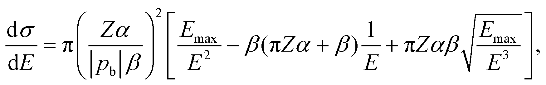 | (1) |
One can then calculate the displacement cross section by integrating dσ/dE over all E large enough to cause a displacement, so that
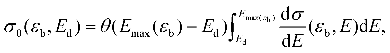 | (2) |
To address the limitations of eqn (2), this work introduces a third party: the material's electrons. Doing so brings two new interactions into play: one between the beam and material electrons and another between material electrons and nuclei. This yields a total of three interactions between the three pairs of particles (Fig. 1). Therefore, the rate of beam-induced sputtering hinges on the rates of three processes mediated by these interactions.
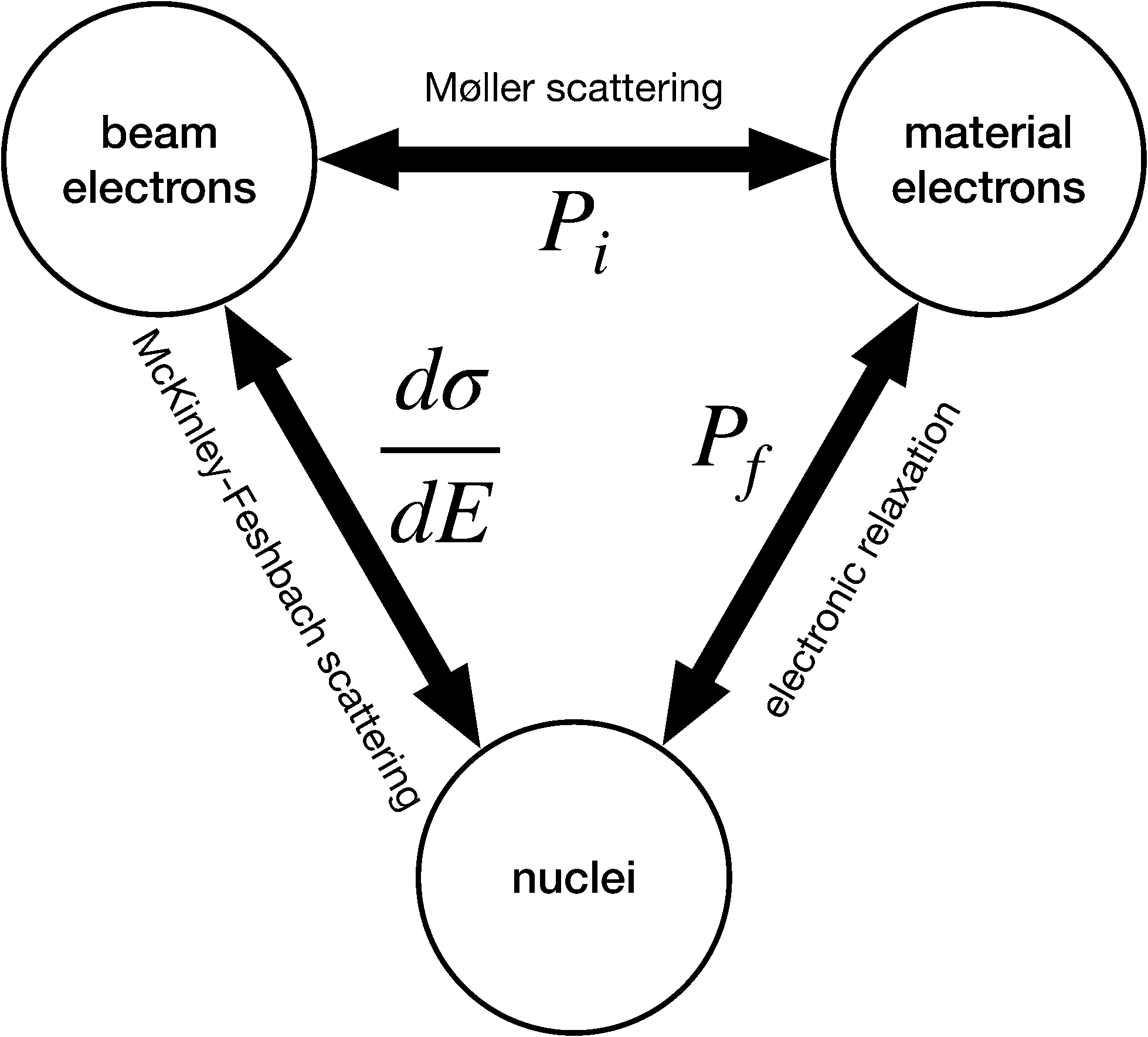 | ||
| Fig. 1 Three interactions between three pairs of particles involved in electron beam-induced sputtering. In insulators, the probability of material electronic excitation (Pi) and the probability that those excitations are substantially long-lived (Pf) can be large. Therefore, the effect of exciting the material electrons on the sputtering rate should not be ignored in these materials. | ||
1. Beam and material electrons: a beam electron can excite some number ni ground state electrons to the conduction band (i denotes the initial interaction with the beam). The probability of this event for a given beam energy εb is Pi(εb,ni).
2. Material electrons and nuclei: some number nf beam-induced excitations can survive long enough for the target atom to leave its original site (f denotes the final system at the completion of sputtering). This depends on the nuclear kinetic energy E and the excitation lifetime τ. The probability that nf of the ni excitations survive is Pf(E,τninf).
3. Beam electrons and material nuclei: the energy transferred to a material nucleus by the beam electron can exceed the PKA's displacement threshold Ed(nf), which depends on the number of surviving excitations nf. We define Ed as the set of all displacement thresholds for all possible nf. Sputtering occurs when E > Ed(nf). The differential cross section for an energy transfer E from the beam electron to material nucleus is dσ/dE(εb,E).
The sputtering cross section can then be calculated by coupling dσ/dE to Pi and Pf for all possible ni and nf. With the terms defined above, this excitation-sensitive sputtering cross section can be written as
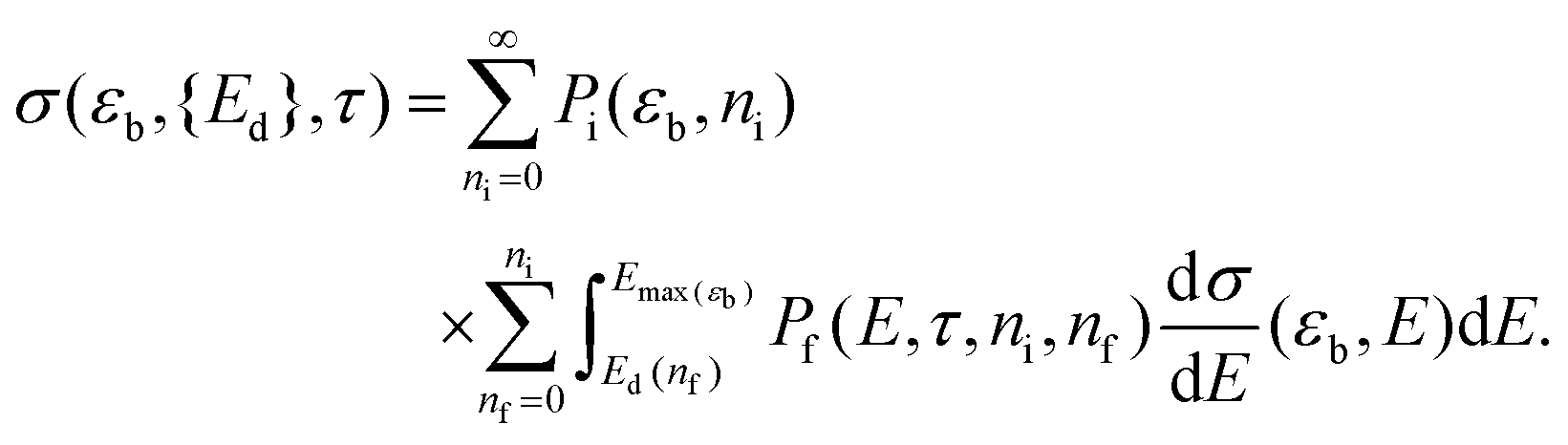 | (3) |
If Pi and Pf are non-negligible when ni and nf are nonzero, and Ed depends strongly on nf, then interactions with the material electrons must be considered. We will later show that this makes σ in eqn (3) larger than σ0 in eqn (2) for all beam energies, most prominently when εb < εc.
The remainder of this section focuses on the derivations of Pi, Pf, and Ed. Section 1 describes how to combine QED with DFT to obtain Pi. Section 2 then considers the evolution of the excited states during the sputtering process to derive Ed and Pf.
2.1. Probability of beam-induced excitation
For a crystal in its ground state, an occupied electron energy eigenstate has zero overlap with any unoccupied state. However, the collision of a beam electron can give an occupied state a momentum boost that breaks this orthogonality. Thus, the boosted ground state has a nonzero probability of being measured in an excited state. We can use this idea to derive Pi(εb,ni), the probability that a beam electron with kinetic energy εb excites exactly ni material electrons. The derivation can be broken down into four steps: (i) determine the amplitude for a free electron to scatter from one momentum eigenstate into another after collision with another free electron; (ii) generalize the formalism to obtain the amplitude for scattering from one wave packet into another by summing over the amplitudes for each momentum component of one wave packet to scatter into each momentum component of the other; (iii) decompose a pair of occupied and unoccupied crystal states into a momentum basis and plug them in as incoming and outgoing wave packets respectively, then square the amplitude to obtain the corresponding excitation probability for a particular transition; (iv) compute the sum of all transition probabilities and use combinatorics to determine Pi(εb,ni). The following subsections address each step (i–iv) in detail.To lowest order, the amplitude for free electron scattering can be represented by two tree-level diagrams, which we call the t- and u-channels (Fig. 2). Using Feynman's rules,17,18 we can write these diagrams in terms of Dirac spinors, yielding the invariant matrix element
 | (4) |
 | ||
| Fig. 2 The lowest order electron–electron scattering perturbation includes two Feynman diagrams called the (a) t-channel and (b) u-channel. The incoming and outgoing electron states are represented by Dirac spinors us(p) and ūs(p) respectively, where p and s are the electron's 4-momentum and spin index respectively. Subscripts 1 and 2 label components of the initial beam and material states respectively. The virtual photon 4-momentum q is the momentum transfer between the electrons. | ||
The first term in brackets is the t-channel describing momentum transfer p3 − p2 and the second is the u-channel describing momentum transfer p4 − p2. Because the DFT cutoff energy (hundreds of eV) is much smaller than the beam energy (tens of keV), it is always the case that |p2| is much smaller than |p1|. Furthermore, we need only consider outgoing momenta for which the kinetic energy associated with either |p3| or |p4| falls within the DFT cutoff energy. In these cases, the magnitude of one outgoing momentum is similar to |p2|, while that of the other is much greater. This means that one channel's momentum transfer is always much larger than the other's. As the momentum transfers reside in the denominators of either channel in eqn (4), it follows that one channel always contributes much more to ![[scr M, script letter M]](https://www.rsc.org/images/entities/char_e145.gif) than the other. Thus, when the t-channel is significant, the u-channel is negligible, and vice versa. Additionally, when integrating over all possible outgoing momenta, the contribution of the t-channel is equal to that of the u-channel. Taking advantage of this along with the indistinguishably of the electrons, we calculate only the t-channel and multiply the resulting amplitude by 2 instead of calculating both channels and adding them. We can then define the 4-momentum transfer between the electrons as that of the t-channel: q ≡ p3 − p2. Because the t-channel has a q2 in the denominator, the resulting scattering probability is proportional to q−4. This makes large momentum transfers statistically irrelevant, allowing us to only consider momentum transfers inside the first Brillouin zone (BZ). The evaluation of the t-channel in terms of the components of the electrons’ 4-momenta is straightforward, though cumbersome, and is described in section S1.†
than the other. Thus, when the t-channel is significant, the u-channel is negligible, and vice versa. Additionally, when integrating over all possible outgoing momenta, the contribution of the t-channel is equal to that of the u-channel. Taking advantage of this along with the indistinguishably of the electrons, we calculate only the t-channel and multiply the resulting amplitude by 2 instead of calculating both channels and adding them. We can then define the 4-momentum transfer between the electrons as that of the t-channel: q ≡ p3 − p2. Because the t-channel has a q2 in the denominator, the resulting scattering probability is proportional to q−4. This makes large momentum transfers statistically irrelevant, allowing us to only consider momentum transfers inside the first Brillouin zone (BZ). The evaluation of the t-channel in terms of the components of the electrons’ 4-momenta is straightforward, though cumbersome, and is described in section S1.†
We can use the resulting to obtain the free electron scattering amplitude
〈p4p3|![[T with combining circumflex]](https://www.rsc.org/images/entities/i_char_0054_0302.gif) |p2p1〉 = (2π)4δ(p1 + p2 − p3 − p4)(p4p3 ← p2p1), |p2p1〉 = (2π)4δ(p1 + p2 − p3 − p4)(p4p3 ← p2p1), | (5) |
is the scattering operator.17,18 This gives the amplitude for two free electrons with momenta p1 and p2 to scatter into p3 and p4. Eqn (5) is used to derive the scattering amplitude between two arbitrary wave packets in the next subsection.
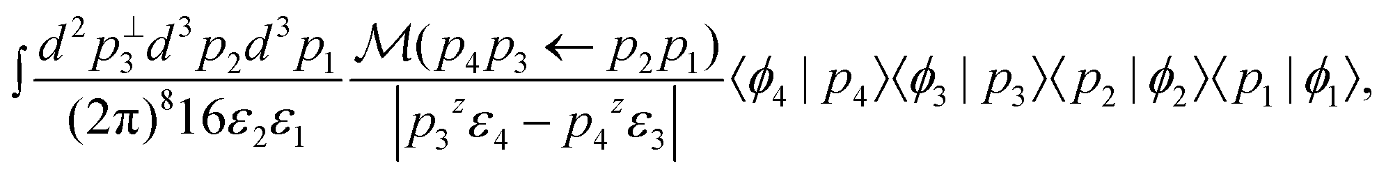
 | (6) |
On the right side, we have inserted two resolutions of the identity given in eqn (S8).† Inserting eqn (5) into the integrand, the amplitude can be written in terms of the invariant matrix element , becoming
 | (7) |
Using the delta function to integrate over p4 and p3z yields
 | (8) |
 | (9) |
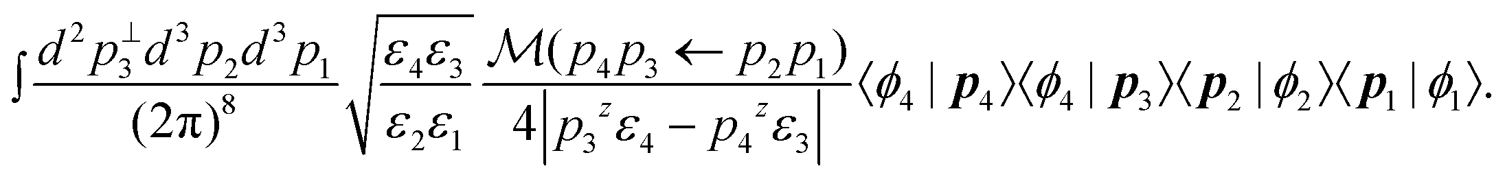
We can then discretize the momenta by replacing d3pi/(2π)3 with V−1 and d2pi⊥/(2π)2 with A−1, where V and A are the volume and cross sectional area of the simulated crystal respectively, i.e., the volume and cross sectional area of the unit cell times the number of k-points used to sample the BZ. With this, the amplitude for electron states |φ1〉 and |φ2〉 to scatter into |φ3〉 and |φ4〉 takes the form
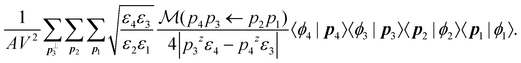 | (10) |
In the next subsection, we replace |φ1…4〉 with states relevant to electron beam-induced excitation.
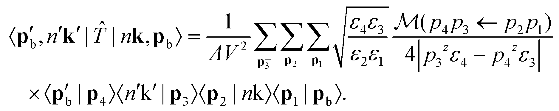 | (11) |
The values of ε1⋯4 need to be clarified before moving forward. The zeroth components of the initial and final beam momenta obey the free particle dispersion relations, so  and
and  . The beam energy that appears in eqn (3) is then defined as the beam electron's total energy minus its rest mass: εb ≡ ε1 − m. Meanwhile, the momentum of the crystal states can be treated nonrelativistically. Thus, the zeroth components of the crystal state momenta are the energy eigenvalues of the crystal state plus the electron rest mass, i.e., ε2 = εnk + m and ε3 = εn′k′ + m. For the remainder of this derivation, we continue to leave our expressions in terms of ε1⋯4 for compactness.
Sputtering from a 2D crystal often requires that the beam electron is backscattered or nearly backscattered, in which case, its final trajectory after collision with the nucleus is nearly antiparallel to its initial trajectory and perpendicular to the crystal surface. Given that many 2D materials (including hBN and MoS2) possess inversion and/or reflection symmetry about the crystal plane, we assume that the likelihood of excitation before and after the collision are about equal. In light of this, we calculate the excitation probability during a sputtering event assuming the beam electron's trajectory is not altered by its collision with the nucleus. That is, we impose that p1 = |p1|ẑ until an electronic excitation is induced.
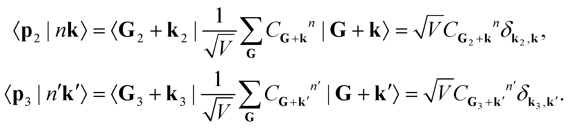
We can now evaluate the bra-ket products in eqn (11). The initial beam state is highly localized on pb, meaning that
| |〈p1|pb〉|2 = Vδp1,pb ⇒ 〈p1|pb〉 = √Vδp1,pb. | (12) |
Meanwhile, the ground and excited crystal states can be expanded into a plane-wave basis, so that
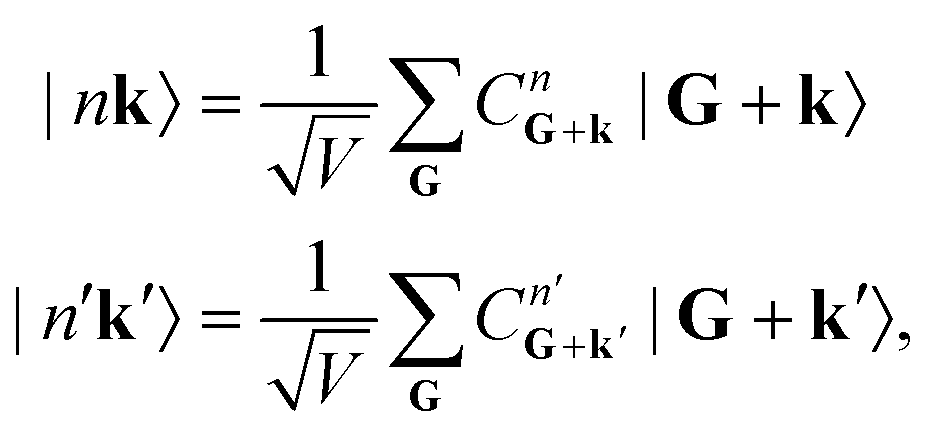 | (13) |
 | (14) |
Lastly, we do not care where the outgoing scattered electron ends up, so we wish for |p′b〉 to satisfy
| |〈p4|p′b〉|2 = V ⇒ |〈p4|p′b〉| = √V. | (15) |
The excitation amplitude is then obtained by plugging in the bra-ket products from eqn (12), (14), and (15) into eqn (11). This gives us the excitation amplitude
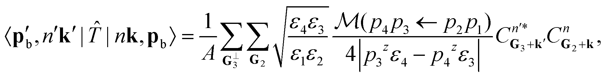 | (16) |
| P(n′k′ ← nk|εb) = |〈p′bn′k′||nk,pb〉|2. | (17) |
 | (18) |
Combinatorics tells us that the probability of exciting exactly one excitation is
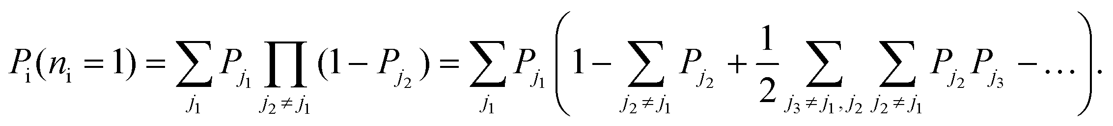 | (19) |
In the large-crystal limit, the number of states, and thus the number of transitions, is large so that the summations over ji in eqn (19) are approximately equal to one another. That is,
 | (20) |
In this limit, the probability of exactly one beam-induced excitation can be written as
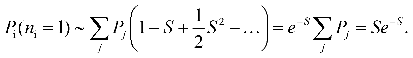 | (21) |
In the same way, the probability of two excitations is
 | (22) |
In general, the probability of exactly ni beam-induced excitations is approximately
 | (23) |
Thus, we see that the probability Pi can be written purely in terms of S.
We can now use formula (23) to calculate excitation probabilities in hBN and (Fig. 3). DFT is used to obtain the plane-wave coefficients CG2+kn and CG3+k′n′ eigenvalues εnk and εn′k′ for the pristine unit cell of each material. These areMoS2 plugged into eqn (16) to obtain the amplitude for each transition. We sum over the squares of all resulting amplitudes to obtain S, which is then plugged into formula (23) to obtain Pi for both materials. We emphasize that the only DFT calculation needed to determine Pi is the electronic structure relaxation of a pristine unit cell, a very inexpensive calculation.
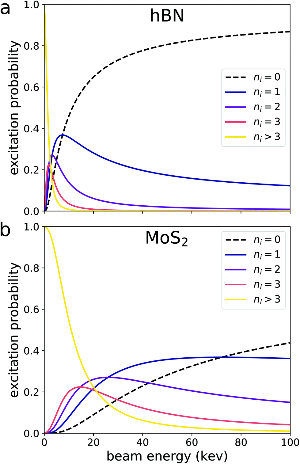 | ||
| Fig. 3 Probabilities of initially exciting a certain number of electrons ni in (a) hBN and (b) MoS2 with a beam electron. The excitation probabilities tend to decreases with increasing beam energy. The excitation probabilities in MoS2 are larger than those in hBN because MoS2 has a significantly smaller band gap. | ||
The probabilities plotted in Fig. 3 reveal some notable trends. First, for sufficiently large beam energies, Pi(εb,ni) decreases with increasing εb for all ni > 0. This is because a faster beam electron has less time to interact with the material and cause an excitation. In this regime, Pi(εb) is proportional to εb−1, a relationship originally predicted by Bethe.12,26,27 This means that multiple excitations are more likely at low beam energies. Furthermore, the probability of remaining in the ground state P(εb,ni = 0) vanishes as εb goes to zero. This implies that a stationary electron in the vicinity of a material is guaranteed to interact with the material's electrons and affect its electronic structure. However, the validity of formula (23) diminishes as εb approaches zero. In the case of a slow beam electron, the interaction between the beam and material electrons can no longer be approximated by the single virtual photon transfer processes depicted in Fig. 2, as the amplitudes for higher-order processes become more significant. The effects of processes beyond the tree-level should be the subject of future work. Lastly, the excitation probability is inversely proportional to the material's band gap. This is because the zeroth component of the momentum transfer q depicted in Fig. 2 is the difference in energy eigenvalues between the occupied and unoccupied states (section 3). Thus, the smallest possible denominator of the t-channel in eqn (4) is proportional to the difference in eigenvalues squared. The experimentally measured band gap of MoS2 is about 1.9 eV (ref. 28) while that of hBN is about 6.1 eV.29 This means MoS2 hosts transitions with smaller eigenvalue differences, making the summands in eqn (16) larger.
With Pi(εb,ni) derived in formula (23) and dσ/dE(εb,E) defined in eqn (1), we now have two of the three functions depicted in Fig. 1 needed to calculate the sputtering cross section in eqn (3). The final ingredients are Pf(E,τninf), the probability that nf excitations survive the displacement event given ni initial beam-induced excitations, and Ed, the set of all displacement thresholds for all nf. The derivations of these objects are described in the next section.
2.2. Sputtering cross section
We have demonstrated how the interaction between the beam and material electrons can induce electronic excitations in the material. In this section, we show how these excitations bring about much larger sputtering cross sections than those predicted by a ground state theory. We start by showing how electronic excitations can reduce the displacement threshold Ed. We then show that longer excitation lifetimes increase Pf for nonzero nf, giving the beam-induced excitations more opportunities to lessen Ed. This motivates us to write the sputtering cross section in eqn (3) analytically in terms of the excitation lifetime τ. Finally, in the next section, the resulting equation is used to predict the sputtering rates of boron and nitrogen in hBN and sulfur in MoS2, which can be made to agree well with experiment for appropriate values of τ for each material.Before describing these assumptions, we first define some important terms. Consider the moment immediately after the beam electron collides with a material nucleus. The nucleus now has a velocity corresponding to the kinetic energy E transferred from the beam electron. The resulting nuclear motion away from its equilibrium position causes the energy of the system to increase. In this sense, the system climbs an energy surface from the bottom of its equilibrium well. Far away from the well's bottom, the energy surface eventually plateaus. If the system reaches this plateau, the displaced PKA moves freely away from its initial site without deceleration. At this point, we consider the PKA to have sputtered. We call the energy at the well's bottom E0 and that at the plateau Es. If the energy surface is static throughout the entire process, then the displacement threshold is simply Ed = Es − E0. When E > Ed, the system has enough energy to climb out of the well, and the PKA sputters. Our task now is to determine how beam-induced excitations in the material electrons and their subsequent relaxation affect E0 and Es. To facilitate this, we make the following assumptions.
Assumption 1: the excited electrons and holes occupy the band edges. To justify this, we shift our focus to the material electrons immediately after the collision. There are now ni electrons in the conduction band and ni holes in the valence bands. Kretschmer et al. simulated the time-evolution of these excitations using Ehrenfest dynamics.12,31 They found that the excited electrons relax nonradiatively to the conduction band minimum (CBM) in a few femtoseconds, while the holes in the valence band take a similar amount of time to relax to the valence band maximum (VBM). In contrast, the PKA takes several hundreds of femtoseconds to fully sputter.7 Thus, the nonradiative relaxation of the electronic structure is essentially instantaneous, and we can assume that all excited electrons and holes occupy the CBM and VBM respectively before the PKA has been displaced by an appreciable amount.
These findings greatly simplify the calculation of E0. Given ni excitations, E0 is just the energy of the pristine system with ni electrons and holes in the CBM and VBM respectively. In the large crystal limit, this amounts to adding the pristine band gap Eg to the system's ground state energy ni times. In other words, E0(ni) = E0(0) + niEg. This approximation of course ignores any binding energy between the electron and hole. However, we believe that this formalism allows for an efficient treatment of the lowest order effects of excitation on E0.
Assumption 2: the fully sputtered system is in its ground state. Finding the plateau energy Es can be a bit more involved. To calculate it properly, one must track how the excitations in the CBM and VBM evolve as the PKA moves away from the crystal. This would require Ehrenfest dynamics of a supercell over timescales of hundreds of femtoseconds for each excitation considered, which is prohibitively expensive. Here we seek a much less costly set of DFT calculations that can still provide a reasonable approximation for Es. To this end, we draw upon another finding of Kretschmer et al.12 After excitation, the displacement of the PKA causes the occupied and unoccupied CBM and VBM states to converge into the band gap and localize on the resulting defect. These converging states are the bonding and antibonding states that connect the PKA to the host crystal. Thus, we should consider how the beam-induced excitations affect the electronic structure on both the PKA and the remaining vacancy.
We start by considering how the ground state eigenvalues evolve as the PKA moves away from the crystal. For hBN, the evolution of eigenvalues differ depending on whether boron or nitrogen is sputtered (Fig. 4). Boron is electropositive while nitrogen is electronegative. Thus, in an hBN crystal, the nitrogen atoms borrow negative charge from the neighboring boron atoms. This means that the p-orbital states that would be occupied on an isolated boron atom are vacant, hovering in the conduction band of hBN. Conversely, the p-orbital states of nitrogen lie occupied in the valence band. For both atoms, separation from the crystal causes those states to converge to degenerate p-orbitals on their respective atoms. When boron is sputtered, these states come from the conduction band. This means that excited electrons residing in the CBM tend to transfer negative charge to the sputtered boron. However, this charge transfer is quite energetically unfavorable since boron is electropositive. The energy cost of this is much larger than the band gap of hBN, compelling any excess electrons on boron to relax to the host crystal. On the other hand, the states that localize on sputtered nitrogen must rise from the valence band. This means that the holes at the VBM tend to transfer positive charge to the sputtered nitrogen, which is again energetically unfavorable for the electronegative atom. Thus, because charge transfer to the sputtered PKA has such a large energy cost, we presume that in most cases, the PKA becomes charge neutral by the time sputtering has occurred.
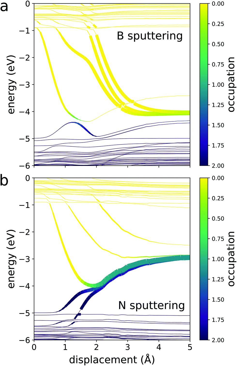 | ||
| Fig. 4 Eigenvalues and occupations of the eigenstates of armchair hBN throughout the sputtering process with respect to the distance between sputtered (a) boron and (b) nitrogen and their pristine sites. The thickness of each curve is proportional to the localization of the corresponding state on the sputtered atom. In hBN, the electronegative nitrogen atoms borrow charge from the neighboring boron atoms. Thus, the p-orbital states that would be occupied on an isolated boron atom reside in the conduction band of hBN and descend into the gap as boron sputters. On the other hand, most of the p-orbital states of nitrogen lie in the valence band and rise into the gap during nitrogen sputtering. | ||
Furthermore, because the states that localize on the PKA converge to the same degenerate p-orbital, the PKA assumes its ground state after it has sputtered, regardless of how many electrons the beam excites. We call the energy of the isolated ground state atom Ea. Meanwhile, the convergence of the bonding and antibonding states localized on the remaining vacancy during the displacement causes the excited electron and hole energy levels to cross multiples times. This means that there are plenty of chances for an excited electron to relax nonradiatively as the PKA separates from the material. Thus, we assume that the host crystal also relaxes to its ground state for most sputtering events.
Lastly, the sputtering threshold is always larger than the vacancy formation energy, because some of the energy transferred to the PKA disperses to the neighboring atoms. For this reason, we calculate the energy of the vacant system without relaxing the structure, as it has been shown that the free energy gained by leaving the structure unrelaxed roughly matches the energy dissipated to the surrounding material.32 We call the energy of the unrelaxed ground state vacancy Ev. Thus, we calculate the plateau energy using Es = Ev + Ea, the sum of the ground state vacancy and isolated atom free energies.
Assumption 3: the PKA velocity is initially constant. Each number of excitations creates its own energy surface. In this way, electronic excitation and relaxation cause the system to hop from surface to surface. In our problem, the initial beam-induced excitation perches the system on an elevated surface. Once there, electronic relaxation via spontaneous emission (SE) enables downward surface hopping at the cost of the emitted photon energy. In this framework, Ed is the energy gained along all energy surfaces that the system traverses during sputtering. For example, suppose the system emits one photon as it sputters. Ed is then the energy gained along the portion of the excited energy surface traversed before emission plus that gained along the relaxed surface after emission. This is how SE can change Ed. However, the effect of SE on Ed must diminish as the PKA moves further away from the crystal. This means there must be some distance d beyond which SE no longer affects the forces on the sputtered atom, leaving the energy surface unchanged. We take d = 4.5 Å in line with Kretschmer et al.'s study, though we acknowledge that the exact meaning of this distance is different in their work.12
We wish to capture this idea while making the calculation of Pf as intuitive as possible. We do this by assuming that each energy surface is constant except for a step when the PKA reaches a distance d away from its equilibrium site. This means that immediately after the collision that excites ni electrons, the surface assumes a constant energy E0(ni). Each relaxation via SE causes the system to drop to the surface beneath it, decreasing its energy by Eg. We define nf as the number of electronic excitations that survive the PKA's traversal of distance d to the energy step. Thus, the energy of the system just before the PKA reaches the step is E0(nf), Beyond the step, all energy surfaces have energy Es, and SE no longer changes the energy surface. With this formalism, Ed is simply the height of the step,
| Ed(nf) = Es − E0(nf) = Ev + Ea − E0(0) − nfEg. | (24) |
Thus we have derived a simple relationship for how electronic excitations affect Ed. However, before we show how this relationship affects the sputtering cross section, we must first point out an important caveat. Eqn (24) suggests that Ed can be negative for large nf. In these cases, the affected atom accelerates away from its pristine site even without energy transfer from the beam electron. This would seem to suggest that the sputtering cross section is infinite, since the PKA would sputter for any energy transfer, no matter how small. This is corroborated by the fact that the integral in eqn (3) diverges as Ed approaches zero, meaning that the sputtering cross section σ would approach infinity. However, this is nonsensical, as it would imply an infinite sputtering rate for a finite beam current. In reality, even though the beam electron does nudge all of the material nuclei to some extent, one nucleus always receives a bigger nudge than the rest. This is the atom onto which the beam-induced excitations localize. Thus, for each beam electron, only one atom's displacement threshold is reduced by electronic excitations. For this reason, the displacement cross section should never exceed the cross sectional area occupied by a single target atom. This means that Ed, the lower integration bound in eqn (3), must have a lower bound itself, which we call Emin. When Ed falls below Emin, we replace it with Emin. We can approximate Emin by setting the displacement cross section in eqn (2) equal to the area occupied by the PKA and solving for the displacement threshold (section S8†). With this, we are finally ready to use eqn (24) to determine the set of displacement thresholds Ed to insert into eqn (3).
All positive displacement thresholds computed for this work are listed in Table 1. Explainations for the calculations of Ev, Ea, E0(0), and Eg are given in subsections 1 and 2. The three largest displacement thresholds for MoS2 with nf = 0, 1, and 2 excitations are similar to those calculated with DFT-based molecular dynamics simulations.12 This provides some assurance that our simplified approach to calculating Ed yields reasonable results. Excitation numbers nf greater than those listed in Table 1 make Ed negative, in which case the exact value of Ed is not important since it is replaced with Emin in the calculation of σ. With that said, it is critical to consider large nf, even if the resulting Ed is less than Emin. These large nf can make appreciable contributions to the total cross section, especially at small beam energies for which Pi(εb,ni) is significant for large ni (Fig. 3). As nf cannot exceed ni, this means that we must consider sufficiently large ni to acknowledge these contributions. Eventually, these contributions diminish as we increment ni, because the ni! in the denominator of Pi in formula (23) eventually outgrows the in the numerator. We can therefore truncate the summation over ni in eqn (3) at some adequately large nimax. This means that nimax must be converged for each material, as materials with greater S require greater nimax. In this work, we choose nimax large enough so that including more excitations increases the sputtering cross section by less than 1% for the smallest experimental beam energy considered for each matieral (Fig. S1†).
| n f | Displacement threshold (eV) | |||
|---|---|---|---|---|
| 0 | 1 | 2 | 3 | |
| B from hBN | 12.85 | 8.78 | 4.71 | 0.64 |
| N from hBN | 12.71 | 8.64 | 4.57 | 0.50 |
| S from MoS2 | 6.92 | 5.04 | 3.16 | 1.28 |
Thus, we have shown how Ed depends only on the number of surviving excitations nf. We must now determine the likelihood that nf excitations survive given ni beam-induced excitations. This is done by comparing the excitation lifetime τ to ts, the time it takes for the PKA to travel a distance d. We handle this task in the next subsection, where we write the sputtering cross section in eqn (3) in terms of τ.
We define the ratio of surviving excitations as
| R(E,τ) = e−ts(E)/τ, | (25) |
 | (26) |
Eqn (26) allows us to rewrite the integral in eqn (3) as
 | (27) |
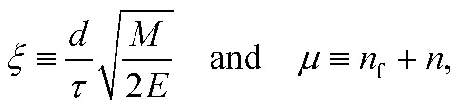
Assumption 3 from the previous subsection again aids us here. Because we posit that the PKA travels at a constant velocity until it reaches the sputtering distance d, we can write ts from eqn (25) quite simply as  . This allows for the straightforward analytical integration of eqn (27). Using dσ/dE defined in eqn (1), the integral on the right can be written as
 | (28) |
 | (29) |
 | (30) |
 | (31) |
 | (32) |
Lastly, the function Ei in eqn (31) is the exponential integral,
 | (33) |
Looking back at eqn (3), we now have everything we need to evaluate the sputtering cross section. We derived Pi(εb,ni) in formula (23), and we performed the integration over E analytically in eqn (27) and (28), setting Ed in eqn (24) as the lower integration bounds. We also have a criterion to truncate the summation over ni at nimax for a given material, as described at the end of section 1. In the following section, we use these results to calculate the sputtering cross sections of hBN and MoS2.
3. Results and discussion
We now apply our theoretical model to calculate the sputtering cross sections of boron and nitrogen from hBN and sulfur from MoS2. In doing so, we show that the consideration of electronic excitations is necessary to make quantitative predictions about beam-induced sputtering rates in 2D insulators.3.1. Boron and nitrogen sputtering from hexagonal BN
Electron beam irradiation has been shown to bore nanopores in monolayer hBN at beam energies far beneath the calculated ground state critical energy of εc ∼ 80 keV.8,9,33,34 In a pristine hBN layer, these beam-induced pores can be initialized from isolated boron and nitrogen vacancies. The atoms surrounding these vacancies have reduced coordination numbers, and thus, smaller displacement thresholds than those in the pristine material. Therefore, the atoms lining the defect are more likely to sputter than their surface counterparts for a given beam energy. As the edge atoms continue to sputter away at a high rate, the nanopore grows, eventually extending up to a few nm in diameter.9,34,35Cretu et al. measured the radial growth of these nanopores under electron irradiation for several temperatures ranging from 673 to 1473 K.9 By dividing the radial growth rate by the beam current, they estimated the sputtering cross section to be around 25 barn under both 30 and 60 keV beams at temperatures of 1273 K and below (Fig. 5c). The cross sections were fairly temperature independent at these relatively low temperatures. Cretu et al. also found that the edges of these pores most often assume an armchair structure. Therefore, in an attempt to reproduce these measurements, we calculate the cross section of boron and nitrogen sputtering from an armchair edge at 1273 K (Fig. 5). To evaluate the displacement thresholds defined in eqn (24) and listed in Table 1, Ev is the free energy of the armchair edge supercell with a single boron or nitrogen vacancy, while Ea is that of an isolated boron or nitrogen atom. E0(0) and Eg are then the calculated free energy and band gap of the pristine armchair edge supercell. We plug the resulting set of displacement thresholds Ed into eqn (3) to calculate the sum of the boron and nitrogen sputtering cross sections. The excitation probabilities of hBN plotted in Fig. 3a are then used for Pi. Strictly speaking, the calculation of Pi should consider the effects of the edge state orbitals. However, in our formalism, the beam electron is in a momentum eigenstate that is highly delocalized in real space. We therefore assume that the radius of the beam is much larger than that of the nanopore. This means that the majority of the beam-matter interactions occur in regions of pristine material, validating the use of the Pi calculated for pristine hBN. Future work should consider the effects of localized beam electron states to simulate beams with smaller focal points. Lastly, temperature effects on the cross section are considered in the manner described in our previous work.7
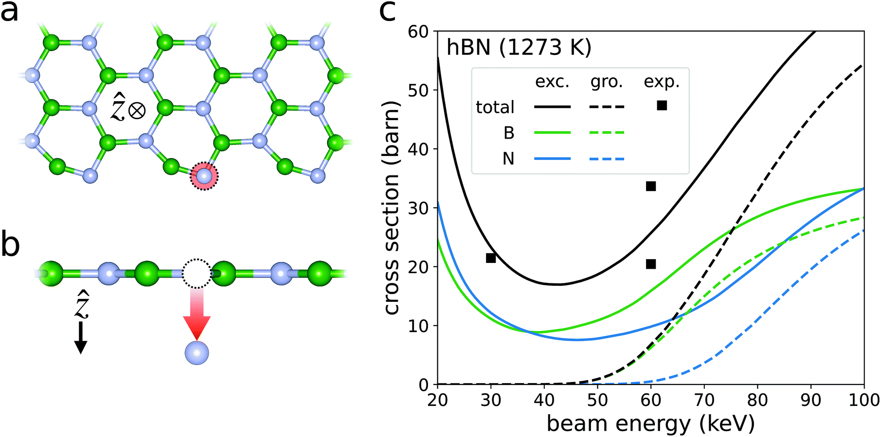 | ||
| Fig. 5 Sputtering from the armchair edge of hBN. The schematics in panels (a) and (b) depict the sputtering of nitrogen from out-of-plane and in-plane perspectives respectively. Panel (c) plots the sputtering cross sections of both boron and nitrogen in green and blue respectively. The black curves are the total sputtering cross section, i.e., the sum of their corresponding blue and green curves. The solid curves account for beam-induced excitations assuming an excitation lifetime of τ = 240 fs (labelled “exc.” for excited). The dashed curves ignore the possibility of beam-induced excitation (labelled “gro.” for ground). The black squares are experimentally observed sputtering cross sections for hBN at 1273 K.9 The consideration of beam-induced excitations reduces the disagreement between theory and experiment substantially. | ||
Fitting our cross section curves to the data of Cretu et al. yields an excellent agreement if the predicted excitation lifetime is set to τ ∼ 240 fs. This predicted lifetime is much shorter than the reported excitation lifetime of ∼0.75 ns in pristine hBN,36 indicating that the sputtering process can significantly reduce the excitation lifetimes of hBN. We suspect that the atomic motion gives rise to non-radiative relaxation pathways that are not explicitly accounted for here. This motivates a closer investigation into the full electronic evolution of the hBN system post-collision. However, such a study is beyond the scope of this work. With that said, the electronic structure in the vicinity of a sputtering PKA differs significantly from that of the pristine room-temperature systems in which excitation lifetimes are experimentally measured. There is therefore no reason to expect the predicted lifetimes in this work to match those obtained by experiments on systems not undergoing sputtering.
We also see that the sputtering cross section, and thus the growth rate of the nanopore, is minimized for beam energies between 30 and 60 keV. Below these energies, the sputtering cross section begins to grow as the beam energy decreases. This is due to a non-negligible probability of final excitation numbers nf > 3, for which Ed(nf) falls below Emin (Table 1). In these cases, the sputtering cross section is Ω ∼ 5 × 10⁸ barn, seven orders of magnitude larger than the measured cross section at 30 keV. This suggests that one can expect the beam-induced nanopores in hBN to grow under beam energies as low as 1 keV. However, one must again be cautious of the predicted cross section at low beam energies in which the tree-level theory starts to break down. Nevertheless, Fig. 5c demonstrates a strong beam-energy dependence in the sputtering cross section across a wide range of experimentally relevant beam-energies. These findings could facilitate precise control of nanopore growth rates in hBN under electron irradiation.
3.2. Sulfur sputtering from MoS2
Kretschmer et al. measured the sputtering cross section of sulfur from MoS2 for several beam energies ranging from 20 to 80 keV.12 They found a peak in the cross section at 30 keV, much less than the predicted ground state εc ∼ 90 keV.12 To help explain this unexpected peak, we calculate the cross section for sulfur sputtering from pristine MoS2 (Fig. 6). The vacant system free energy Ev for the calculation of Ed is that of a MoS2 supercell with a single sulfur vacancy. Ea is then the free energy of an isolated sulfur atom, and E0(0) is that of the pristine MoS2 supercell. We then set Eg equal to the experimental band gap of 1.88 eV.28 Using the resulting Ed, we find that summing over the contributions of final excitation numbers nf > 2 to the sputtering cross section produces a peak just below 30 keV, matching Kretschmer et al.'s findings remarkably well. In fitting to this peak, we predict an excitation lifetime of τ ∼ 81 fs. This is again much shorter than the excitation lifetime of pristine MoS2, which is on the order of a few picoseconds.37–39 However, this is also much shorter than the fitted lifetime of hBN found in the previous subsection, consistent with the fact that the excitation lifetime of pristine hBN is much longer than that of MoS2.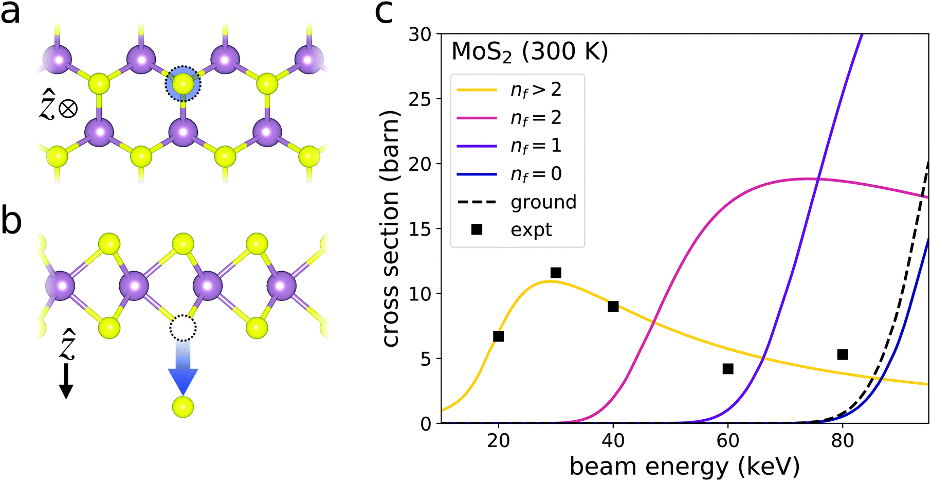 | ||
| Fig. 6 Sputtering of sulfur from the outgoing MoS2 surface. The sputtering of molybdenum from MoS2 can be ignored because its displacement threshold is significantly larger than that of sulfur. The schematics in panels (a) and (b) depict the sputtering process from out-of-plane and in-plane perspectives respectively. Panel (c) plots the contributions of various numbers of final excitations nf to the sputtering cross section assuming an excitation lifetime of τ = 81 fs. The black dashed curve plots the predicted cross section ignoring the possibility of beam-induced excitation. The black squares are experimentally observed cross sections at 300 K.12 The contribution from the sum of all nf > 2 final excitations matches the experimental cross section remarkably well. | ||
The difference between the two materials’ lifetimes leads to markedly dissimilar cross section behaviors at low beam energies. Below beam energies of 30 keV, the cross section of MoS2 gradually drops to zero with decreasing εb. In contrast, hBN's total cross section has a minimum at around 40 keV and begins to increase as εb decreases. Eventually, hBN's sputtering cross section peaks before dropping quickly to zero as the beam energy goes to zero (Fig. S2†). However, this peak occurs at around 0.5 keV, far below the lower energy bound of Fig. 5c. These distinct cross section behaviors can be explained by the amplified sensitivity of nf to τ at low beam energies. Eqn (25) and (26) tell us that larger τ makes large nf more likely. At the same time, nf cannot exceed ni. Thus, nf is more sensitive to τ at low beam energies for which ni is large. Accordingly, because τ is greater in hBN than in MoS2, the expected values of nf in hBN are much larger than those of MoS2 at low beam energies. This explains why the effect of considering excitations is much more pronounced in hBN than in MoS2. Furthermore, the difference in the cross section behavior is exacerbated by the fact that sulfur is heavier than both boron and nitrogen, so that its post-collision velocity is always smaller for a given energy transfer E. It follows that ts is larger, and thus, Pf is smaller for a given E in MoS2. This again increases the likelihood that hBN has more final excitations than MoS2, meaning that the effects of beam-induced excitation on hBN's sputtering cross section are greater.
We also plot the contributions of nf = 0, 1, and 2 excitations to MoS2's sputtering cross section separately. In doing so, we see that the contributions of nf = 1 or 2 would conceal the peak at 30 keV. Thus, it seems that the likelihoods of nf = 1 or 2 are somehow suppressed. This suggests that the individual beam-induced excitations and subsequent relaxation are in some cases correlated. That is, the excitation and/or relaxation rates of a given electronic transition are affected by the coinciding distribution of electronic excitations. Thus, a proper treatment of these excitations and their effect on the sputtering cross section requires that the excitation probabilities of every possible transition are calculated for every possible excitation configuration. Such a nonlinear calculation is beyond the scope of this work, but should certainly be pursued in a future study. Nonetheless, the methods laid out here demonstrate that the consideration of beam-induced excitation can provide a quantitative justification for the sulfur sputtering rate to peak at a beam energy well-below the expected ground state critical energy.
4. Conclusions
In this paper, we developed a first-principles method to more accurately describe electron beam-induced sputtering cross sections in 2D insulating crystals by accounting for beam-induced electronic excitations and their subsequent relaxations. The method combines QED scattering theory with DFT electronic structure calculations to determine the likelihood of beam-induced excitation. The results show that the excitation probability is inversely proportional to both the material's band gap and beam electron's kinetic energy. We then show how these nonzero excitation probabilities increase the predicted sputtering cross sections of both hBN in MoS2. These cross sections can be made quantitatively similar to those obtained experimentally by treating the excitation lifetime as a fitting parameter. The methods laid out are computationally efficient, requiring only a few ground state electronic optimization calculations for each cross section curve. Thus, the formalism that we have developed can be easily applied to any 2D crystalline material to simulate the rates of atomic displacement under electron irradiation.With that said, several questions naturally arise from our study. For example, why is the excitation lifetime reduced so drastically during sputtering? How might excitation and relaxation rates of different transitions be correlated? How might preexisting defects affect those rates? These questions urge follow up work to address the full breadth of physical processes involved in beam-matter interactions. Future studies should also consider additional electronic relaxation pathways to determine their effect on Pf. Correspondingly, other electronic responses such as ionization, core excitations, and second order electronic excitation effects such as Auger scattering can be incorporated into the calculation of Pi.38,40–42 Moreover, spin polarization effects can also be examined by making spin-dependent, i.e., not averaging over spins as is done in eqn (4). The beam electron path can also change significantly after collision with the nucleus. Ensuing research should investigate how these altered trajectories generate new excitation probabilities Pi, which must certainly play a role in 3D bulk materials as well as layered and confined 2D systems.43–46 Furthermore, the methods here can be modified to accommodate more advanced DFT techniques. For example, the calculation of Pi should be made compatible with ultrasoft and projector augmented wave pseudopotentials47 in a manner similar to that employed in modern GW codes.48–50 In addition, the plane-wave coefficients of excited electronic states can be calculated self-consistently using constrained DFT.51 Perhaps most importantly, progress in this field requires much more experimental data. We therefore hope this paper encourages new experimental investigation into beam-induced sputtering for beam energies below the predicted ground state critical energy.
Clearly, the combined QED-DFT approach to modeling beam-induced excitations and their effect on the sputtering cross section opens up a rich and diverse field of physics for both theoretical and experimental exploration. We hope that this work and the work it may stimulate can eventually enable the use of electron beams for precise atomic-scale engineering of crystalline materials.
5. Computational details
DFT13,14 was used to calculate (i) the plane wave coefficients CG+kn and eigenvalues εnk of each material's electronic orbitals to determine the excitation probabilities (section 2.1.3) and (ii) the free energies of the pristine and sputtered structures to determine the displacement thresholds for sputtering (section 2.2.1).Plane-wave coefficients and eigenvalues were calculated using Quantum ESPRESSO.52 Because eqn (16) relies on the orthogonality of the Kohn–Sham orbitals, the optimized norm-conserving Vanderbilt pseudopotentials53,54 were employed. The sum of all transition probabilities S defined in eqn (18) was used to gage the convergence of all parameters, which were deemed converged when any increase in precision changed S by less than 5% (Fig. S5†). The cutoff energies for hBN and MoS2 were set to 490 and 408 eV respectively. While these cutoffs are lower than what is typically used for norm-conserving psuedopotentials, both cutoffs yield well-converged values of S (Fig. S5b and e†). Meanwhile, the hBN and MoS2 unit cells were given heights of 18 and 12 Å respectively. For both materials, the maximum virtual photon momentum |qmax| required for convergence fell well within their first BZs. We therefore chose |qmax| to be the magnitude of high-symmetry point K in each respective BZ. The maximum number of initial excitations considered for hBN and MoS2 were nimax = 5 and 9 respectively (Fig. S1†). Finally, convergence of S requires extremely dense k-point sampling of the BZ. This necessitates fitting a curve to S calculated for various k-point mesh densities and extrapolating to an infinitely fine mesh to estimate the converged value of S (section S6†). The most dense k-point meshes used to fit these curves had dimensions of 45 × 45 × 1 and 36 × 36 × 1 for hBN and MoS2 respectively, corresponding to very similar linear k-point spacings of 0.056 and 0.055 Å−1 respectively.
Next, free energy calculations were carried out with the Vienna ab initio Simulation Package (VASP)15,55 implementing the projector augmented wave (PAW) method47 along with the Perdew–Burke–Ernserhof (PBE) generalized gradient approximation (GGA) to the exchange correlation functional.56 van der Waals interactions were accounted for using the optB88-vdW density functional methods.57,58 All parameters were converged so that any increase in precision would change the total free energy by less than 1 meV per atom. The parameter values that satisfy this criteria generally differed from those listed in the previous paragraph. The cutoff energies for hBN and MoS2 were set to 800 and 550 eV respectively, while the BZs of both materials’ pristine unit cells were sampled with Γ-centered 6 × 6 × 1 Monkhorst–Pack meshes,59 corresponding to linear k-point spacings of 0.417 and 0.328 Å−1 for hBN and MoS2 respectively. To achieve the same k-point densities, surface vacancies in MoS2 and edge vacancies in hBN were placed in respective 6 × 6 × 1 and 4 × 1 × 1 supercells whose BZs were sampled with a single k-point on Γ. The heights of the hBN and MoS2 cells were 12 Å and 20 Å respectively to provide sufficient separation from periodic images. Nanoribbon structures were used to simulate isolated armchair edges in hBN. These ribbons were more than 16 Å across and placed in cells 28 Å wide to avoid interactions between opposing edges and periodic images. Lastly, relaxation iterations of ionic positions and lattice constants persisted until the all Hellmann–Feynman forces settled below 1 meV Å−1.
Author contributions
AY and ML designed the code used to calculate the excitation probabilities and their effect on the sputtering cross section. AY and JG developed the theoretical model to describe beam-induced electronic excitation. AY, DL, JJ, PG, TY, BGS, and VM, developed the theoretical model to describe how excitations affect the sputtering cross section. AY carried out all calculations.Conflicts of interest
There are no conflicts to declare.Acknowledgements
Calculations were performed at the Center for Computational Innovations at Rensselaer Polytechnic Institute, Livermore Computing Center at Lawrence Livermore National Laboratory (LLNL), and Compute and Data Environment for Science at Oak Ridge National Laboratory (ORNL), which is supported by the Office of Science of the U.S. Department of Energy (DOE) under Contract No. DE-AC05-00OR22725. This work was performed under the auspices of the U.S. Department of Energy by LLNL under Contract DE-AC52-07NA27344. This material is also based upon work supported by the U.S. DOE, Office of Science, Office of Workforce Development for Teachers and Scientists, Office of Science Graduate Student Research (SCGSR) program. The SCGSR program is administered by the Oak Ridge Institute for Science and Education for the DOE under contract number DE-SC0014664. Funding was provided by the National Science Foundation (Award 1608171). Work (BGS, PG, DL, JJ) was also supported by ORNL's Center for Nanophase Materials Sciences, a U.S. DOE Office of Science User Facility.References
- F. Banhart, Rep. Prog. Phys., 1999, 62, 1181–1221 CrossRef CAS.
- R. F. Egerton, Ultramicroscopy, 2013, 127, 100–108 CrossRef CAS PubMed.
- X. Zhao, J. Kotakoski, J. C. Meyer, E. Sutter, P. Sutter, A. V. Krasheninnikov, U. Kaiser and W. Zhou, MRS Bull., 2017, 42, 667–676 CrossRef CAS.
- T. Susi, J. C. Meyer and J. Kotakoski, Nat. Rev. Phys., 2019, 1, 397–405 CrossRef.
- J. C. Meyer, F. Eder, S. Kurasch, V. Skakalova, J. Kotakoski, H. J. Park, S. Roth, A. Chuvilin, S. Eyhusen, G. Benner, A. V. Krasheninnikov and U. Kaiser, Phys. Rev. Lett., 2012, 108, 196102–196107 CrossRef PubMed.
- T. Susi, C. Hofer, G. Argentero, G. T. Leuthner, T. J. Pennycook, C. Mangler, J. C. Meyer and J. Kotakoski, Nat. Commun., 2016, 7, 13040 CrossRef CAS PubMed.
- A. Yoshimura, M. Lamparski, N. Kharche and V. Meunier, Nanoscale, 2018, 10, 2388–2397 RSC.
- J. Kotakoski, C. H. Jin, O. Lehtinen, K. Suenaga and A. V. Krasheninnikov, Phys. Rev. B: Condens. Matter Mater. Phys., 2010, 82, 113404 CrossRef.
- O. Cretu, Y. C. Lin and K. Suenaga, Micron, 2015, 72, 21–27 CrossRef CAS PubMed.
- Y.-C. Lin, T. Björkman, H.-P. Komsa, P.-Y. Teng, C.-H. Yeh, F.-S. Huang, K.-H. Lin, J. Jadczak, Y.-S. Huang, P.-W. Chiu, A. V. Krasheninnikov and K. Suenaga, Nat. Commun., 2015, 6, 6736–6741 CrossRef CAS PubMed.
- T. Lehnert, O. Lehtinen, G. A. Siller, U. Kaiser, G. Algara-Siller and U. Kaiser, Appl. Phys. Lett., 2017, 110, 033106 CrossRef.
- S. Kretschmer, T. Lehnert, U. Kaiser, A. V. Krasheninnikov and A. V. Krasheninnikov, Nano Lett., 2020, 20, 2865–2870 CrossRef CAS PubMed.
- P. Hohenberg and W. Kohn, Phys. Rev., 1964, 136, B864–B871 CrossRef.
- W. Kohn and L. J. Sham, Phys. Rev., 1965, 140, A1133–A1138 CrossRef.
- G. Kresse and J. Furthmüller, Phys. Rev. B: Condens. Matter Mater. Phys., 1996, 54, 11169–11186 CrossRef CAS PubMed.
- H. Lourenço-Martins, A. Lubk and M. Kociak, SciPost Phys., 2021, 10, 31 CrossRef.
- M. E. Peskin and D. V. Schroeder, An Introduction to Quantum Field Theory, Perseus Books Publishing, L.L.C., Reading, MA, 1st edn, 1995 Search PubMed.
- T. Lancaster and S. J. Blundell, Quantum Field Theory for the Gifted Amateur, Oxford University Press, New York, NY, United States of America, 1st edn, 2014, p. 350 Search PubMed.
- N. F. Mott, Proc. R. Soc. A, 1929, 124, 425–442 CAS.
- W. A. McKinley and H. Feshbach, Phys. Rev., 1948, 74, 1759–1763 CrossRef CAS.
- O. S. Oen, Cross sections for atomic displacements in solids by fast electrons, Oak ridge national laboratory technical report, 1973 Search PubMed.
- R. F. Egerton, R. McLeod, F. Wang and M. Malac, Ultramicroscopy, 2010, 110, 991–997 CrossRef CAS.
- C. Møller, Ann. Phys., 1932, 406, 531–585 CrossRef.
- H. Kragh, Arch. Hist. Exact Sci., 1992, 43, 299–328 CrossRef.
- X. Roqué, Arch. Hist. Exact Sci., 1992, 44, 197–264 CrossRef.
- H. Bethe, Ann. Phys., 1930, 397, 325–400 CrossRef.
- M. Inokuti, Y.-K. Kim and R. L. Platzman, Phys. Rev., 1967, 164, 55–61 CrossRef CAS.
- J. Gusakova, X. Wang, L. L. Shiau, A. Krivosheeva, V. Shaposhnikov, V. Borisenko, V. Gusakov and B. K. Tay, Phys. Status Solidi, 2017, 214, 1700218 CrossRef.
- C. Elias, P. Valvin, T. Pelini, A. Summerfield, C. J. Mellor, T. S. Cheng, L. Eaves, C. T. Foxon, P. H. Beton, S. V. Novikov, B. Gil and G. Cassabois, Nat. Commun., 2019, 10, 2639 CrossRef CAS PubMed.
- D. B. Lingerfelt, P. Ganesh, J. Jakowski and B. G. Sumpter, Adv. Funct. Mater., 2019, 1901901, 1901901 CrossRef.
- X. Li, J. C. Tully, H. B. Schlegel and M. J. Frisch, J. Chem. Phys., 2005, 123, 84106 CrossRef PubMed.
- H. P. Komsa, J. Kotakoski, S. Kurasch, O. Lehtinen, U. Kaiser and A. V. Krasheninnikov, Phys. Rev. Lett., 2012, 109, 035503 CrossRef PubMed.
- C. Jin, F. Lin, K. Suenaga and S. Iijima, Phys. Rev. Lett., 2009, 102, 195505 CrossRef PubMed.
- J. C. Meyer, A. Chuvilin, G. Algara-Siller, J. Biskupek and U. Kaiser, Nano Lett., 2009, 9, 2683–2689 CrossRef CAS PubMed.
- M. Dogan, S. M. Gilbert, T. Pham, B. Shevitski, P. Ercius, S. Aloni, A. Zettl and M. L. Cohen, Appl. Phys. Lett., 2020, 117, 9–13 CrossRef.
- J. Li, X. K. Cao, T. B. Hoffman, J. H. Edgar, J. Y. Lin and H. X. Jiang, Appl. Phys. Lett., 2016, 108, 122101 CrossRef.
- T. Korn, S. Heydrich, M. Hirmer, J. Schmutzler, C. Schüller and C. Schller, Appl. Phys. Lett., 2011, 99, 102109 CrossRef.
- D. Lagarde, L. Bouet, X. Marie, C. R. Zhu, B. L. Liu, T. Amand, P. H. Tan and B. Urbaszek, Phys. Rev. Lett., 2014, 112, 47401 CrossRef CAS PubMed.
- M. Palummo, M. Bernardi and J. C. Grossman, Nano Lett., 2015, 15, 2794–2800 CrossRef CAS PubMed.
- D. Kozawa, R. Kumar, A. Carvalho, K. Kumar Amara, W. Zhao, S. Wang, M. Toh, R. M. Ribeiro, A. H. Castro Neto, K. Matsuda and G. Eda, Nat. Commun., 2014, 5, 4543 CrossRef CAS PubMed.
- Z. Nie, R. Long, J. S. Teguh, C.-C. Huang, D. W. Hewak, E. K. L. Yeow, Z. Shen, O. V. Prezhdo and Z.-H. Loh, J. Phys. Chem. C, 2015, 119, 20698–20708 CrossRef CAS.
- H. Shi, R. Yan, S. Bertolazzi, J. Brivio, B. Gao, A. Kis, D. Jena, H. G. Xing and L. Huang, ACS Nano, 2013, 7, 1072–1080 CrossRef CAS PubMed.
- W. Wang, Y. Zheng, X. Li, Y. Li, H. Zhao, L. Huang, Z. Yang, X. Zhang and G. Li, Adv. Mater., 2019, 31, 1803448 CrossRef PubMed.
- A. Kakanakova-Georgieva, G. K. Gueorguiev, D. G. Sangiovanni, N. Suwannaharn, I. G. Ivanov, I. Cora, B. Pécz, G. Nicotra and F. Giannazzo, Nanoscale, 2020, 12, 19470–19476 RSC.
- A. Kakanakova-Georgieva, F. Giannazzo, G. Nicotra, I. Cora, G. K. Gueorguiev, P. O. Å. Persson and B. Pécz, Appl. Surf. Sci., 2021, 548, 149275 CrossRef CAS.
- Z. Wang, G. Wang, X. Liu, S. Wang, T. Wang, S. Zhang, J. Yu, G. Zhao and L. Zhang, J. Mater. Chem. C, 2021, 9, 17201–17232 RSC.
- P. E. Blöchl, Phys. Rev. B: Condens. Matter Mater. Phys., 1994, 50, 17953–17979 CrossRef PubMed.
- M. Shishkin and G. Kresse, Phys. Rev. B: Condens. Matter Mater. Phys., 2006, 74, 035101 CrossRef.
- M. Gajdoš, K. Hummer, G. Kresse, J. Furthmüller and F. Bechstedt, Phys. Rev. B: Condens. Matter Mater. Phys., 2006, 73, 045112 CrossRef.
- J. Paier, R. Hirschl, M. Marsman and G. Kresse, J. Chem. Phys., 2005, 122, 234102 CrossRef PubMed.
- B. Kaduk, T. Kowalczyk and T. Van Voorhis, Chem. Rev., 2012, 112, 321–370 CrossRef CAS PubMed.
- P. Giannozzi, S. Baroni, N. Bonini, M. Calandra, R. Car, C. Cavazzoni, D. Ceresoli, G. L. Chiarotti, M. Cococcioni, I. Dabo, A. D. Corso, S. de Gironcoli, S. Fabris, G. Fratesi, R. Gebauer, U. Gerstmann, C. Gougoussis, A. Kokalj, M. Lazzeri, L. Martin-Samos, N. Marzari, F. Mauri, R. Mazzarello, S. Paolini, A. Pasquarello, L. Paulatto, C. Sbraccia, S. Scandolo, G. Sclauzero, A. P. Seitsonen, A. Smogunov, P. Umari and R. M. Wentzcovitch, J. Phys.: Condens. Matter, 2009, 21, 395502 CrossRef PubMed.
- D. R. Hamann, Phys. Rev. B: Condens. Matter Mater. Phys., 2013, 88, 85117 CrossRef.
- M. Schlipf and F. Gygi, Comput. Phys. Commun., 2015, 196, 36–44 CrossRef CAS.
- G. Kresse and J. Furthmüller, Comput. Mater. Sci., 1996, 6, 15–50 CrossRef CAS.
- J. P. Perdew, K. Burke and M. Ernzerhof, Phys. Rev. Lett., 1996, 77, 3865–3868 CrossRef CAS PubMed.
- J. Klimeš, D. Bowler and A. Michaelides, J. Phys.: Condens. Matter, 2009, 22, 022201–022205 CrossRef PubMed.
- J. Klimeš, D. R. Bowler and A. Michaelides, Phys. Rev. B: Condens. Matter Mater. Phys., 2011, 83, 195131 CrossRef.
- H. Monkhorst and J. Pack, Phys. Rev. B: Solid State, 1976, 13, 5188–5192 CrossRef.
Footnotes |
| † Electronic supplementary information (ESI) available: Derivation of the invariant matrix element introduced in eqn (4), description of the normalization scheme used for the integral in eqn (6), derivation of pz3 that conserves energy and momentum, convergence of σ with respect to nimax, peaks in the sputtering cross section of hBN for low beam energies, fitting and convergence of S with respect to various parameters, derivation of the minimum energy transfer Emin mentioned after eqn (24), and details on the derivation of . See DOI: https://doi.org/10.1039/d2nr01018f |
| ‡ In remembrance of our dear friend and colleague, Prof. Tao Yu. Deceased 13.06.2021 |
| This journal is © The Royal Society of Chemistry 2023 |