DOI:
10.1039/D3NH00207A
(Communication)
Nanoscale Horiz., 2023,
8, 1395-1402
Interplay of the charge density wave transition with topological and superconducting properties†
Received
30th May 2023
, Accepted 12th July 2023
First published on 18th July 2023
Abstract
Exotic phenomena due to the interplay of different quantum orders have been observed and the study of these phenomena has emerged as a new frontier in condensed matter research, especially in the two-dimensional limit. Here, we report the coexistence of charge density waves (CDWs), superconductivity, and nontrivial topology in monolayer 1H-MSe2 (M = Nb, Ta) triggered by momentum-dependent electron–phonon coupling through electron doping. At a critical electron doping concentration, new 2 × 2 CDW phases emerge with nontrivial topology, Dirac cones, and van Hove singularities. Interestingly, these 2 × 2 CDW phases are also superconducting. Our findings not only reveal a route towards realizing nontrivial electronic characters by CDW engineering, but also provide an exciting platform to modulate different quantum states at the confluence of CDWs, superconductivity, nontrivial topology, and electron–phonon coupling.
New concepts
The combination of topological physics and electron–phonon coupling (EPC) in quantum materials has emerged as a new frontier of condensed matter research. Here, we report that electron-doped 1H-NbSe2 and 1H-TaSe2 are charge density waves (CDWs) with nontrivial topology and superconductivity. In addition, EPC is demonstrated to play a central role in both the formation of these new CDWs and the change of the superconducting critical temperatures. The EPC-driven topological phase transitions in this work provide an avenue to understand the interplay between many-body instabilities and topology, which can inspire the finding of new topologically nontrivial superconductors in the future.
|
1. Introduction
Many-body instabilities and topological physics are two attractive topics in condensed matter research.1–3 It is interesting to explore the interplay between these phenomena in a single quantum material,4–6 which leads to many exotic properties. For example, the Weyl nodes in (TaSe4)2I are opened by charge density wave (CDW) transition below 263 K, resulting in an axion insulator.4,7 On the other hand, pressure-driven superconductivity in Weyl semimetal WTe2 and MoTe2 allows their topological edge states to be superconducting, which can be useful for quantum computation.5,8 Furthermore, the coexistence of CDWs, superconductivity, and nontrivial topology has been reported in the recently discovered Kagome metals AV3Sb5 (A = K, Rb, and Cs).9,10 The electronic bands near the Fermi energy of AV3Sb5 are fascinating and feature both Dirac cones and van Hove singularities (VHSs).11–13 Such novel electronic structures are characterized by odd Z2 indices,10 which can stimulate the anomalous Hall effect in a frustrated magnetic sublattice.14 Besides, the in-plane 2 × 2 CDW and superconducting orders occur below the respective critical temperatures.10,15 Their formation mechanisms and mutual interplay have generated tremendous attention.16–18 However, the coexistence of these quantum orders in AV3Sb5 stems from the unique Kagome lattice, which hinders the further exploration of this frontier. Therefore, it is urgently desired to realize rich electronic characters in materials with a trivial electronic band.
CDW engineering opens a new era for manipulating electronic characters. CDWs are a symmetry-breaking phenomenon below the transition temperature TCDW.19 The band folds in its reduced Brillouin zone (BZ) provide an opportunity to form Dirac cones. Besides, the subtle lattice distortion of a CDW phase can further modify the electronic structure.20 More importantly, CDW distortion is very sensitive to external stimuli, which provides great flexibility for modulating the electronic and phononic properties by CDW transition.21,22 Because of the large specific surface area, CDWs in two-dimensional (2D) materials are particularly sensitive to external stimuli and can be easily manipulated. New exotic phenomena induced by external stimuli triggered CDW transition await to be explored.
Monolayer 1H-NbSe2 and 1H-TaSe2 are hot 2D transition metal dichalcogenides (TMDs) that draw a great deal of attention due to the many-body instabilities.23–32 NbSe2 and TaSe2 in the following refer to the monolayer phase unless stated otherwise. NbSe2 undergoes a CDW transition with 3 × 3 periodic distortion at TCDW ∼ 145 K as well as a superconducting transition at TC ∼ 3 K.28 Similar 3 × 3 CDW and superconductivity also exist in TaSe2 with TCDW ∼ 130 K32 and TC ∼ 2.2 K,33 respectively. Recent experiments indicate that NbSe2 becomes a 2 × 2 CDW under electron doping,34 while such transition has not been reported for TaSe2 yet. More importantly, the mechanism for this CDW transition and the electronic properties of the 2 × 2 CDW structure are still elusive.
In this work, based on first-principles calculations and mean-field theory, we identify 1H-MSe2 (M = Nb, Ta) as an ideal platform to investigate CDWs, superconductivity, and topology, which are all sensitive to carrier concentration. Momentum-dependent electron–phonon coupling (q-EPC) is found to account for the phase transition from 3 × 3 to 2 × 2 CDW under electron doping. We determine two possible 2 × 2 CDW structures, which may exist when the doping concentration reaches 0.2 electrons per formula unit (e−/f.u.). Besides, our study explores the effects of electron doping on the CDW gaps and density of states (DOS) at the Fermi surface. In addition, electron doping produces opposite effects on superconductivity in NbSe2 and TaSe2. The superconducting transition temperature decreased in NbSe2 while increased in TaSe2. Our investigation suggests that the variation of the total electron–phonon coupling (EPC) strength under doping is responsible for this opposite trend in superconductivity. Moreover, we find in both NbSe2 and TaSe2, that one of their two 2 × 2 CDW phases is topologically nontrivial with Dirac cones and van Hove singularities. These results show that monolayer NbSe2 and TaSe2 can be an EPC-driven CDW with nontrivial topology and superconductivity.
2. Results and discussion
2.1. A CDW transition under electron doping
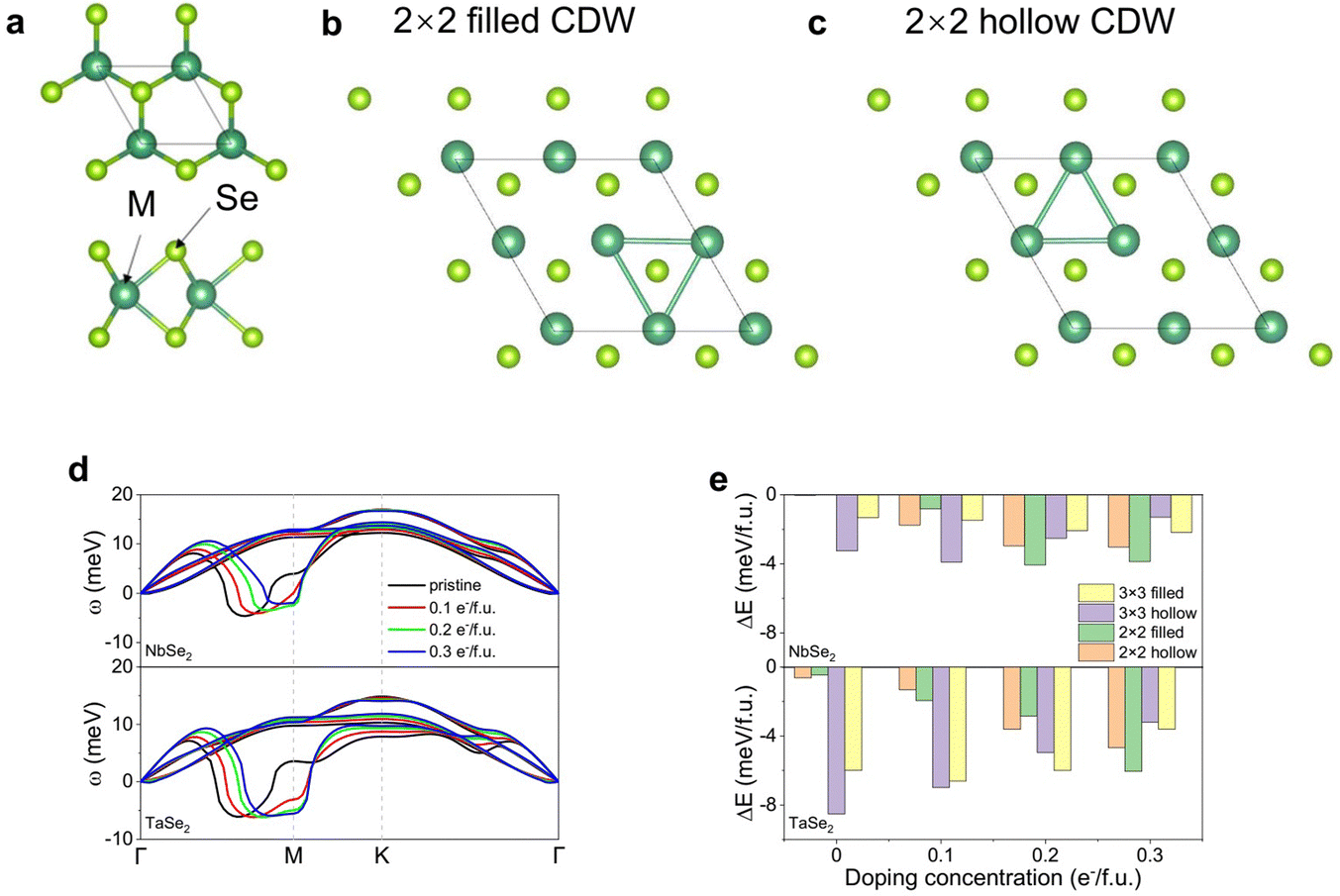
The structure of normal monolayer 1H-MSe2 (M = Nb, Ta) is shown in Fig. 1a, which has a P![[6 with combining macron]](https://www.rsc.org/images/entities/char_0036_0304.gif) m2 space group. The metal atoms are sandwiched between two Se layers with the trigonal prismatic cells. The phonon dispersion of normal MSe2 (M = Nb, Ta) displays imaginary frequencies around 2/3ΓM (Fig. 1d), suggesting the formation of a 3 × 3 CDW. And it has been argued that there are two possible 3 × 3 CDW structures (Fig. S2g and h, ESI†), which are coined as 3 × 3 hollow and 3 × 3 filled CDW structures with cation clusters centered on the hollow sites and Se atoms of the honeycomb lattice, respectively.20,35,36 With the increase of electron doping concentration, the position of imaginary phonons gradually evolves from 2/3ΓM to the M point (Fig. 1d), which implies transition from 3 × 3 to 2 × 2 CDW. Similarly, we found two possible 2 × 2 CDW structures when the doping concentrations are above 0.2 e−/f.u., and we denote them as 2 × 2 filled (Fig. 1b) and 2 × 2 hollow (Fig. 1c) CDW structures according to the location of the centers of the cation clusters.
m2 space group. The metal atoms are sandwiched between two Se layers with the trigonal prismatic cells. The phonon dispersion of normal MSe2 (M = Nb, Ta) displays imaginary frequencies around 2/3ΓM (Fig. 1d), suggesting the formation of a 3 × 3 CDW. And it has been argued that there are two possible 3 × 3 CDW structures (Fig. S2g and h, ESI†), which are coined as 3 × 3 hollow and 3 × 3 filled CDW structures with cation clusters centered on the hollow sites and Se atoms of the honeycomb lattice, respectively.20,35,36 With the increase of electron doping concentration, the position of imaginary phonons gradually evolves from 2/3ΓM to the M point (Fig. 1d), which implies transition from 3 × 3 to 2 × 2 CDW. Similarly, we found two possible 2 × 2 CDW structures when the doping concentrations are above 0.2 e−/f.u., and we denote them as 2 × 2 filled (Fig. 1b) and 2 × 2 hollow (Fig. 1c) CDW structures according to the location of the centers of the cation clusters.
 |
| | Fig. 1 (a) Schematic diagram of normal MSe2 (M = Nb, Ta) monolayer in the top and side views. (b) 2 × 2 filled and (c) 2 × 2 hollow CDW structures. (d) The phonon spectra of NbSe2 (up) and TaSe2 (down) under different electron doping concentrations. Since the optical phonon modes hardly change, we only show acoustic phonon modes for the systems. (e) The formation energies for the 3 × 3 filled, 3 × 3 hollow, 2 × 2 filled, and 2 × 2 hollow CDW structures as a function of electron doping concentration. The high-symmetry points are indicated in Fig. S1 (ESI†). | |
To further verify CDW transitions under electron doping, the energetic hierarchy of these CDW structures is calculated at various doping concentrations. The CDW formation energies ΔE are calculated by ECDW/x − E0, where ECDW and E0 are the total energies of the CDW and the 1 × 1 normal phases, respectively, and x is the number of formula units in the CDW phase. Within the doping concentration range studied in this work, Fig. 1e clearly shows transitions from 3 × 3 hollow CDWs to 2 × 2 filled CDWs in both NbSe2 and TaSe2 at a critical doping concentration of around 0.2 e−/f.u., in agreement with phonon calculations (Fig. 1d).
2.2. CDW transition mechanism
Although there are some preliminary results for the understanding of the CDW formation in bulk 2H-MSe2, a systematic and quantitative analysis for 2D counterparts is still missing. This is particularly important given the potential changes that may occur in the 2D limit, where the reduced dimensionality typically enhances the nesting condition, and the electron doping suppresses intraband screening to weaken the coupling between electrons and phonons. As such, it is crucial to investigate the formation mechanism for monolayer 2 × 2 CDWs under electron doping.
It is known that the softened phonon frequency ωq can be obtained by:37,38
where
Ωq is the bare phonon frequency, and
Πq is the real part of the phonon self-energy, the latter of which carries the information from both EPC and Fermi surface nesting (FSN). In the static limit,
Πq has the form:
| |  | (2) |
Here,
f(
εk) is the Fermi–Dirac function with energy
ε at the
k point, and
gk,k+q is the EPC matrix element, which can be calculated via:
39| |  | (3) |
where
φk is the electronic wavefunction with wavevector
k, and
V is the Kohn–Sham potential. The imaginary phonon frequency, suggesting a CDW formation, appears when
Πq is larger than (1/2)
Ωq. The peak location of
Πq corresponds to the dip position of
ωq, which can be converted to the CDW vector in the reciprocal space, and the CDW lattice in the real space.
21 Due to the low energy physics studied in this work, the coupling is considered between the softened phonon branch and the single electronic band which crosses the Fermi level (Fig. S2a and d, ESI
†). Taking |
gk,k+q|
2 ∼ |
gq|
2, which is known as
q-EPC and can be extracted from
Πq to represent the EPC contribution,
26 the remaining part is:
| |  | (4) |
where
χq is the real part of the bare electronic susceptibility, which captures the Fermi surface topology as the FSN effect.
40
Fig. 2a and e display the distribution of the softened phonon frequency ωq in the first BZs of NbSe2 and TaSe2 under 0.3 e−/f.u. doping concentration, respectively. The distribution of imaginary phonon frequencies (see the dark blue areas in Fig. 2a and e) clearly shows a valley shape centered at the M points. Meanwhile, complementary patterns can be found for the peak of the real part of the phonon self-energy Πq (see the yellow areas in Fig. 2b and f). Furthermore, we decompose the contribution of the real part of the phonon self-energy Πq into the pure effect of EPC and FSN by calculating |gq|2 and χq separately. For doped cases, it is interesting to note that |gq|2 and Πq have very similar patterns in the first BZs, both of which have maxima at M (Fig. 2b, c, f and g). However, their χq display peaks around 1/2ΓM (Fig. 2d and h), which deviates from the dips of ωq in Fig. 2a and e and the peaks of Πq in Fig. 2b and f. Thus, |gq|2 provides the main contribution to Πq and determines the pattern of phonon softening, confirming q-EPC as the driving force for the doped 2 × 2 CDW formation. Furthermore, combining the pristine CDW formation analyses in SI–III (ESI†), we conclude that q-EPC is responsible for the CDW transition from 3 × 3 to 2 × 2 CDW under electron doping.
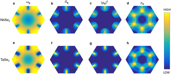 |
| | Fig. 2 (a) The softened phonon frequency ωq, (b) the real part of the phonon self-energy Πq, (c) q-EPC |gq|2 and (d) the real part of the bare electronic susceptibility χq in the first BZ of NbSe2 under 0.3 e−/f.u. doping concentration. (e)–(h) Same as panels (a)–(d) but for TaSe2 under 0.3 e−/f.u. doping concentration. | |
2.3. Electronic structures near the Fermi surface
The Fermi surface of the pristine NbSe2 3 × 3 hollow CDW is shown in Fig. 3a, which displays full CDW gaps in the K pockets. Such electronic gap opening also decreases the DOS at the Fermi level NF (Fig. 3c). When NbSe2 is under electron doping, the shrinkage of the K pocket is accompanied by a transition from a full to partial gap opening. Meanwhile, the electronic states at the Fermi level increase, as shown in Fig. 3c. The pristine 3 × 3 hollow CDW of TaSe2 displays a similar Fermi surface to NbSe2. However, the spectral intensity of the K pocket becomes more blurred (Fig. 3d), corresponding to the greater reduction in NF (Fig. 3f). After the electron doping, the K pocket becomes more pronounced (Fig. 3e), which is also reflected in the enhancement of NF (Fig. 3f).
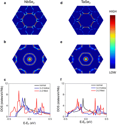 |
| | Fig. 3 (a) The simulated Fermi surface of pristine NbSe2 in the ground-state 3 × 3 CDW phase. (b) The simulated Fermi surface of NbSe2 in the ground-state 2 × 2 CDW phase under 0.3 e−/f.u. doping concentration. (c) Electronic DOS of the normal, 3 × 3 hollow CDW for pristine NbSe2 and 2 × 2 filled CDW under 0.3 e−/f.u. doping concentration. (d)–(f) Same as panels (a)–(d) but for TaSe2. The Fermi surfaces of the normal phases of NbSe2 and TaSe2 are shown in Fig. S2b, c and e, f (ESI†), respectively. | |
2.4. Superconductivity under electron doping
The superconductivity of the NbSe2 CDW is further explored. According to the Allen–Dynes modified McMillan theory,39 the Eliashberg spectral function is obtained by:| |  | (5) |
where λqν is the EPC strength of phonon mode ν with momentum q, and ωqν is the phonon frequency. The total EPC strength is given by:| | 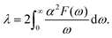 | (6) |
The superconducting transition temperature TC can be calculated by:| |  | (7) |
Here, ωlog is the logarithmically averaged phonon frequency, and μ* is the effective Coulomb parameter which is estimated from the DOS at the Fermi energy: μ* ≈ 0.26NF/(1 + NF).6,41
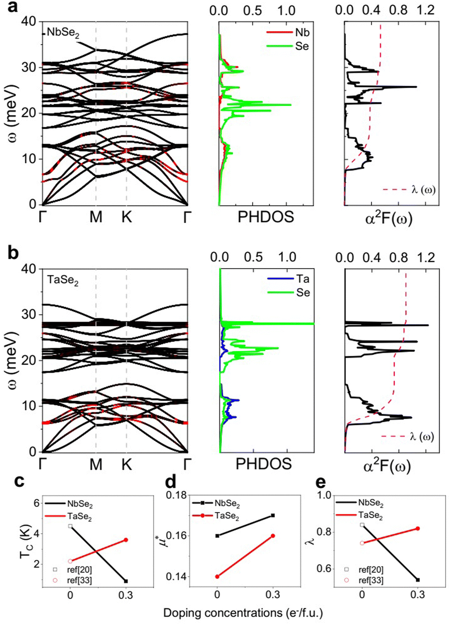
Fig. 4a and b show the calculated phonon spectra of 2 × 2 filled CDWs for NbSe2 and TaSe2, respectively, under 0.3 e−/f.u. doping concentration. The absence of an imaginary phonon frequency indicates the stability of these two structures. Fig. 4a shows that the Se vibrations concentrate on the middle-frequency region (i.e., 17–22 meV), while the Nb and Se atoms have similar contributions to the phonon DOS (PHDOS) outside this region. It is noted that the phonons between 8 meV and 15 meV have strong EPC strength λqν, and these phonons contribute 67% of the total λ. Combined with the high-frequency region contributions, the total λ of the doped NbSe2 2 × 2 filled CDW is calculated to be 0.54 (Fig. 4a). Using μ* = 0.17 estimated from NF, we obtain TC = 0.9 K for the doped NbSe2 CDW. The phonon spectrum of the doped TaSe2 CDW is less dispersive than that of the doped NbSe2 CDW with the highest phonon frequency changed from 37 meV for NbSe2 to 32 meV for TaSe2 (Fig. 4a and b), due to the heavier mass of Ta atoms.42 In addition, Ta vibrations mainly provide the low-frequency PHDOS between 6 meV and 15 meV, further contributing to 75% of the total λ with the help of strong EPC strength λqν in this region (Fig. 4b). The high-frequency region is dominated by Se vibrations, which contribute 25% to the total λ. Thus, the total λ and TC of the doped TaSe2 2 × 2 filled CDW is calculated to be 0.82 and 3.6 K, respectively. Such TC is close to the intrinsic superconducting transition temperature in other VB group 2D TMDs, including 1H-NbS2 and 1H-TaS2, both of which have TC around 3 K.43,44
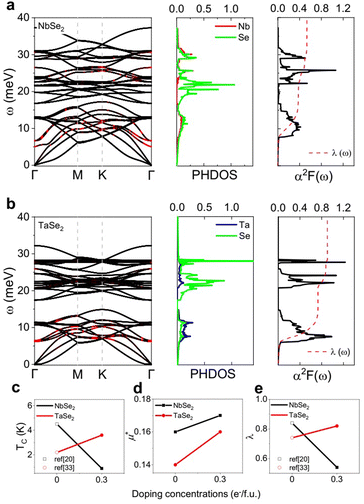 |
| | Fig. 4 (a) The phonon spectrum, PHDOS, Eliashberg spectral function α2F(ω) and frequency-dependent integrated EPC λ(ω) of the 2 × 2 filled CDW under 0.3 e−/f.u. doping concentration for NbSe2. The phonon spectrum highlighted in red indicates the strong EPC strength λqν. (b) Same as panel (a) but for TaSe2. Comparison of (c) the superconducting transition temperature TC, (d) the effective Coulomb parameter μ* and (e) the total EPC strength λ between the pristine 3 × 3 hollow CDW and 0.3 e−/f.u. doped 2 × 2 filled CDW. The calculated TC and λ for pristine CDWs are used for comparison.20,33 | |
Interestingly, although CDWs in both NbSe2 and TaSe2 have been suppressed under electron doping, the superconductivity of NbSe2 and TaSe2 displays an opposite trend. The calculated TC of NbSe2 changes from 4.5 K to 0.9 K, while that of TaSe2 increases from 2.2 K to 3.6 K (Fig. 4c). To gain physical insight into this difference, we start with the BCS theory. According to the BCS theory, the phonon-mediated electrons form Cooper pairs to overcome Coulomb repulsion between electrons. In particular, the Coulomb repulsion between paired electrons is represented by μ*,45 while the electron–phonon interaction is evaluated by λ.46
Fig. 4d shows that the effective Coulomb parameter μ* for both NbSe2 and TaSe2 increases under electron doping. This is reasonable as electron doping reduced the plasmon energy and enhances the effective Coulomb repulsion.33,47 However, the effective Coulomb repulsion is detrimental to the formation of superconductivity as it retards the formation of Coulomb pairs. In addition, the increment of μ* in both NbSe2 and TaSe2 cannot explain the opposition in superconducting temperature transitions.
Another mechanism that must be considered is electron–phonon interaction. The total λ of NbSe2 has been reduced 36% to 0.54 through doping, while in doped TaSe2, the total λ increases 11% to 0.82. The trend of the total λ is consistent with the trend of the transition temperature TC. Therefore, we propose that the EPC plays an important role in the change of superconductivity under electron doping.
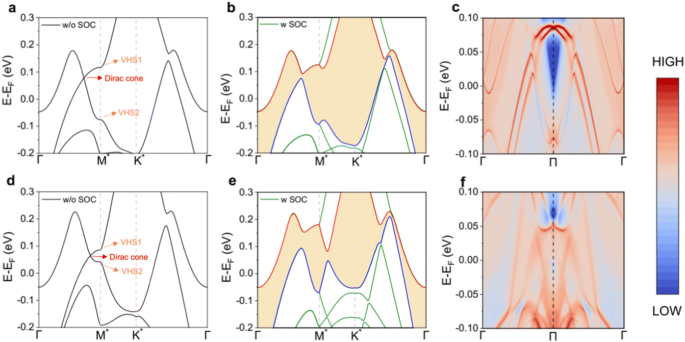
Fig. 5a and d show the electronic band structure of the 2 × 2 hollow CDWs of NbSe2 and TaSe2 without spin–orbital coupling (SOC), where Weyl nodes are protected by the mirror symmetry on the ΓM* path. Besides, two VHSs emerge at their M points. The combination of the Dirac cone and VHSs in the vicinity of the Fermi level is strongly reminiscent of the band of the Kagome metal, which drives diverse correlated phenomena.12,48,49 The SOC opens a band gap of about 15 meV and 59 meV (Fig. 5b and e), resulting in the nontrivial topological phases in NbSe2 and TaSe2. The trivial bands overlapping with topological Dirac bands allow the identification of a Z2 topological metal, which is essential for the coexistence of topological and superconducting properties.50 A material with both surface topological Dirac cones and bulk superconductivity may intrinsically establish the proximity effect, which has promising applications.51 According to the bulk-edge correspondence, the nonzero Z2 = 1 invariant is closely related to the nontrivial helical edge states that emerge inside the gap between two energy bands in a semi-infinite system. As presented in Fig. 5c and f, there are Dirac cone edge states emerging within the continuous nontrivial band gap. Furthermore, the 2 × 2 hollow CDW phases for NbSe2 and TaSe2 are also superconductors with TC = 1.2 K and 4.4 K, respectively (see details in the SI–IV, ESI†). Therefore, the 2 × 2 hollow CDW phases are 2D superconductors with clearly visible topological edge states near the Fermi level, which are rarely reported in 2D systems. More importantly, in marked contrast to the exotic electronic structure rooted in the peculiar Kagome lattices, the one presented here is induced by CDW engineering, which can be easily achieved in experiments.34,52–54 This could be a general strategy and applied to other systems.
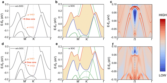 |
| | Fig. 5 The band structures of the NbSe2 2 × 2 hollow CDW under 0.3 e− f.u.−1 doping concentration (a) without and (b) with SOC. The continuous band gap is shaded. (c) The edge states of the 2 × 2 hollow CDW are projected on the (100) edge. Red colors indicate higher local DOS and blue colors represent the bulk band gap. (d)–(f) Same as panels (a)–(c) but for TaSe2. The high symmetry points are indicated in Fig. S1 (ESI†). | |
3. Conclusion
In conclusion, we first demonstrate that CDW engineering can be a convenient technique to modulate topology and superconductivity, to the best of our knowledge. The formation of 2 × 2 CDWs is caused by the modulation of q-EPC under electron doping, which also weakens the CDW gap opening. In addition, the superconducting transition temperature decreases in doped NbSe2 while increasing in doped TaSe2. This is understood by the change of the total EPC strength λ under electron doping. Thus, we propose that EPC plays a dominant role in both CDW and superconductivity under doping. Prominently, the 2 × 2 hollow CDW phases for both NbSe2 and TaSe2 under 0.3 e−/f.u. doping concentration are superconductors with nontrivial topology, suggesting that CDW engineering based on the modulation of q-EPC is a powerful tool to introduce nontrivial electronic properties. Our work not only deepens the understanding of CDW, but also presents a guide for developing topological and superconducting properties. Future works should apply the same strategy to other CDW materials, using the high-throughput method to discover topological electrons and phonons induced by CDW engineering.
4. Method
The first-principles calculations were performed using the Quantum Espresso package55,56 with a norm-conserving pseudopotential.57 The vacuum layer was set to be 15 Å to minimize the interaction between adjacent layers. The plane wave energy cutoff was 80 Ry. All geometries were relaxed until residual forces and the energy difference are smaller than 4 × 10⁻⁶ Ry/bohr and 10−10 Ry, respectively. A Gamma centered 16 × 16 × 1 (8 × 8 × 1) and 8 × 8 × 1 (4 × 4 × 1) k-grid (q-grid) was chosen for the calculations of normal phase and 2 × 2 CDW phases, respectively. The EPW code58 was employed for the electron–phonon coupling property with fine k and q meshes of 64 × 64 × 1. The real part of the bare electronic susceptibility was calculated at CDW transition temperature 145 K with a 111 × 111 × 1 electron-momentum grid. The electron doping was simulated by adding electrons to the system with a compensating uniform positive background. Considering that the lattice of NbSe2 is pinned by the substrate in the experiments, the structures were re-optimized with the same lattice constant under different doping concentrations. The edge states were calculated by using the Wannier functions and the iterative Green's function method.59–62
Author contributions
Z. W. conceived the idea. Z. W., J. Y., and C. C. performed the calculations, and wrote the manuscript under the guidance of J. Z., K. P. L., and Y. P. F. All authors contributed to the discussion and the revision of the manuscript.
Conflicts of interest
The authors declare no competing financial or non-financial interests.
Acknowledgements
C. C. is thankful for the support from Shuimu Tsinghua Scholar Program. This research project was funded by the Ministry of Education, Singapore, under its MOE AcRF Tier 3 Award MOE2018-T3-1-002, and MOE AcRF Tier 2 Award MOE2019-T2-2-030. Computations were supported by the Center of Advanced 2D Materials (CA2DM) HPC infrastructure.
References
- S. Manzeli, D. Ovchinnikov, D. Pasquier, O. V. Yazyev and A. Kis, Nat. Rev. Mater., 2017, 2, 17033 CrossRef CAS.
- X. L. Qi and S. C. Zhang, Rev. Mod. Phys., 2011, 83, 1057 CrossRef CAS.
- G. Grüner, Rev. Mod. Phys., 1988, 60, 1129 CrossRef.
- W. Shi, B. J. Wieder, H. L. Meyerheim, Y. Sun, Y. Zhang, Y. Li, L. Shen, Y. Qi, L. Yang, J. Jena, P. Werner, K. Koepernik, S. Parkin, Y. Chen, C. Felser, B. A. Bernevig and Z. Wang, Nat. Phys., 2021, 17, 381 Search PubMed.
- Y. Qi, P. G. Naumov, M. N. Ali, C. R. Rajamathi, W. Schnelle, O. Barkalov, M. Hanfland, S. C. Wu, C. Shekhar, Y. Sun, V. Süβ, M. Schmidt, U. Schwarz, E. Pippel, P. Werner, R. Hillebrand, T. Förster, E. Kampert, S. Parkin, R. J. Cava, C. Felser, B. Yan and S. A. Medvedev, Nat. Commun., 2016, 7, 11038 Search PubMed.
- X. Xi, H. Berger, L. Forró, J. Shan and K. F. Mak, Phys. Rev. Lett., 2016, 117, 106801 CrossRef PubMed.
- J. Gooth, B. Bradlyn, S. Honnali, C. Schindler, N. Kumar, J. Noky, Y. Qi, C. Shekhar, Y. Sun, Z. Wang, B. A. Bernevig and C. Felser, Nature, 2019, 575, 315–319 CrossRef CAS PubMed.
- X. C. Pan, X. Chen, H. Liu, Y. Feng, Z. Wei, Y. Zhou, Z. Chi, L. Pi, F. Yen, F. Song, X. Wan, Z. Yang, B. Wang, G. Wang and Y. Zhang, Nat. Commun., 2015, 6, 7805 CrossRef PubMed.
- H. Tan, Y. Liu, Z. Wang and B. Yan, Phys. Rev. Lett., 2021, 127, 046401 CrossRef CAS PubMed.
- B. R. Ortiz, S. M. L. Teicher, Y. Hu, J. L. Zuo, P. M. Sarte, E. C. Schueller, A. M. M. Abeykoon, M. J. Krogstad, S. Rosenkranz, R. Osborn, R. Seshadri, L. Balents, J. He and S. D. Wilson, Phys. Rev. Lett., 2020, 125, 247002 CrossRef CAS PubMed.
- S. Cho, H. Ma, W. Xia, Y. Yang, Z. Liu, Z. Huang, Z. Jiang, X. Lu, J. Liu, Z. Liu, J. Li, J. Wang, Y. Liu, J. Jia, Y. Guo, J. Liu and D. Shen, Phys. Rev. Lett., 2021, 127, 236401 CrossRef CAS PubMed.
- Y. Hu, X. Wu, B. R. Ortiz, S. Ju, X. Han, J. Ma, N. C. Plumb, M. Radovic, R. Thomale, S. D. Wilson, A. P. Schnyder and M. Shi, Nat. Commun., 2022, 13, 2220 CrossRef CAS PubMed.
- S. RbV, Z. Liu, N. Zhao, Q. Yin, C. Gong, Z. Tu, M. Li, W. Song, Z. Liu, D. Shen, Y. Huang, K. Liu, H. Lei and S. Wang, Phys. Rev. X, 2021, 11, 041010 Search PubMed.
- S. Y. Yang, Y. Wang, B. R. Ortiz, D. Liu, J. Gayles, E. Derunova, R. Gonzalez-Hernandez, L. Šmejkal, Y. Chen, S. S. P. Parkin, S. D. Wilson, E. S. Toberer, T. McQueen and M. N. Ali, Sci. Adv., 2020, 6, eabb6003 CrossRef CAS PubMed.
- K. Nakayama, Y. Li, T. Kato, M. Liu, Z. Wang, T. Takahashi, Y. Yao and T. Sato, Phys. Rev. X, 2022, 12, 011001 CAS.
- K. Y. Chen, N. N. Wang, Q. W. Yin, Y. H. Gu, K. Jiang, Z. J. Tu, C. S. Gong, Y. Uwatoko, J. P. Sun, H. C. Lei, J. P. Hu and J. G. Cheng, Phys. Rev. Lett., 2021, 126, 247001 CrossRef CAS PubMed.
- Q. Wang, P. Kong, W. Shi, C. Pei, C. Wen, L. Gao, Y. Zhao, Q. Yin, Y. Wu, G. Li, H. Lei, J. Li, Y. Chen, S. Yan and Y. Qi, Adv. Mater., 2021, 33, 2102813 CrossRef CAS PubMed.
- Y. Song, T. Ying, X. Chen, X. Han, X. Wu, A. P. Schnyder, Y. Huang, J. G. Guo and X. Chen, Phys. Rev. Lett., 2021, 127, 237001 CrossRef CAS PubMed.
- K. Rossnagel, J. Phys.: Condens. Matter, 2011, 23, 213001–213025 CrossRef CAS PubMed.
- C. S. Lian, C. Si and W. Duan, Nano Lett., 2018, 18, 2924–2929 CrossRef CAS PubMed.
- Z. Wang, J. Zhou, K. P. Loh and Y. P. Feng, Appl. Phys. Lett., 2021, 119, 163101 CrossRef CAS.
- L. J. Li, E. C. T. O’Farrell, K. P. Loh, G. Eda, B. Özyilmaz and A. H. Castro Neto, Nature, 2016, 529, 185–189 CrossRef CAS PubMed.
- T. Kiss, T. Yokoya, A. Chainani, S. Shin, T. Hanaguri, M. Nohara and H. Takagi, Nat. Phys., 2007, 3, 720–725 Search PubMed.
- F. Flicker and J. Van Wezel, Nat. Commun., 2015, 6, 7034 Search PubMed.
- A. Soumyanarayanan, M. M. Yee, Y. He, J. Van Wezel, D. J. Rahn, K. Rossnagel, E. W. Hudson, M. R. Norman and J. E. Hoffman, Proc. Natl. Acad. Sci. U. S. A., 2013, 110, 1623 CrossRef CAS PubMed.
- X. Zhu, Y. Cao, J. Zhang, E. W. Plummer and J. Guo, Proc. Natl. Acad. Sci. U. S. A., 2015, 112, 2367 CrossRef CAS PubMed.
- S. Gao, F. Flicker, R. Sankar, H. Zhao, Z. Ren, B. Rachmilowitz, S. Balachandar, F. Chou, K. S. Burch, Z. Wang, J. van Wezel and I. Zeljkovic, Proc. Natl. Acad. Sci. U. S. A., 2018, 115, 6986–6990 CrossRef CAS PubMed.
- X. Xi, L. Zhao, Z. Wang, H. Berger, L. Forró, J. Shan and K. F. Mak, Nat. Nanotechnol., 2015, 10, 765–769 CrossRef CAS PubMed.
- M. M. Ugeda, A. J. Bradley, Y. Zhang, S. Onishi, Y. Chen, W. Ruan, C. Ojeda-Aristizabal, H. Ryu, M. T. Edmonds, H. Z. Tsai, A. Riss, S. K. Mo, D. Lee, A. Zettl, Z. Hussain, Z. X. Shen and M. F. Crommie, Nat. Phys., 2016, 12, 92 Search PubMed.
- X. Xi, Z. Wang, W. Zhao, J. H. Park, K. T. Law, H. Berger, L. Forró, J. Shan and K. F. Mak, Nat. Phys., 2016, 12, 139–143 Search PubMed.
- D. Lin, S. Li, J. Wen, H. Berger, L. Forró, H. Zhou, S. Jia, T. Taniguchi, K. Watanabe, X. Xi and M. S. Bahramy, Nat. Commun., 2020, 11, 2406 Search PubMed.
- H. Ryu, Y. Chen, H. Kim, H. Z. Tsai, S. Tang, J. Jiang, F. Liou, S. Kahn, C. Jia, A. A. Omrani, J. H. Shim, Z. Hussain, Z. X. Shen, K. Kim, B. Il Min, C. Hwang, M. F. Crommie and S. K. Mo, Nano Lett., 2018, 18, 689–694 CrossRef CAS PubMed.
- C. S. Lian, C. Heil, X. Liu, C. Si, F. Giustino and W. Duan, J. Phys. Chem. Lett., 2019, 10, 4076–4081 CrossRef CAS PubMed.
- R. T. Leriche, A. Palacio-morales, M. Campetella, C. Tresca, S. Sasaki, C. Brun, F. Debontridder, P. David, I. Arfaoui, O. Šofranko, T. Samuely, G. Kremer, C. Monney, T. Jaouen, L. Cario, M. Calandra and T. Cren, Adv. Funct. Mater., 2021, 31, 2007706 CrossRef CAS.
- G. Gye, E. Oh and H. W. Yeom, Phys. Rev. Lett., 2019, 122, 016403 CrossRef CAS PubMed.
- E. Oh, G. Gye and H. W. Yeom, Phys. Rev. Lett., 2020, 125, 036804 CrossRef CAS PubMed.
- F. Flicker and J. Van Wezel, Phys. Rev. B, 2016, 94, 235135 CrossRef.
- Z. Wang, C. Chen, J. Mo, J. Zhou, K. P. Loh and Y. P. Feng, Phys. Rev. Res., 2023, 5, 013218 CrossRef CAS.
- F. Giustino, Rev. Mod. Phys., 2017, 89, 015003 CrossRef.
- M. D. Johannes and I. I. Mazin, Phys. Rev. B: Condens. Matter Mater. Phys., 2008, 77, 165135 CrossRef.
- F. Zheng and J. Feng, Phys. Rev. B, 2019, 99, 161119(R) CrossRef.
- W. Chu, Q. Zheng, O. V. Prezhdo, J. Zhao and W. A. Saidi, Sci. Adv., 2020, 6, 7453–7467 CrossRef PubMed.
- Z. Wang, C. Y. Cheon, M. Tripathi, G. M. Marega, Y. Zhao, H. G. Ji, M. Macha, A. Radenovic and A. Kis, ACS Nano, 2021, 15, 18403–18410 CrossRef CAS PubMed.
- S. C. De La Barrera, M. R. Sinko, D. P. Gopalan, N. Sivadas, K. L. Seyler, K. Watanabe, T. Taniguchi, A. W. Tsen, X. Xu, D. Xiao and B. M. Hunt, Nat. Commun., 2018, 9, 1427 CrossRef PubMed.
- K.-H. Lee, K. J. Chang and M. L. Cohen, Phys. Rev. B: Condens. Matter Mater. Phys., 1995, 52, 1425 CrossRef CAS PubMed.
- W. L. McMillan, Phys. Rev., 1968, 167, 326–331 CrossRef.
- P. Cudazzo, M. Gatti and A. Rubio, Phys. Rev. B: Condens. Matter Mater. Phys., 2012, 86, 075121 CrossRef.
- M. Kang, S. Fang, J. K. Kim, B. R. Ortiz, S. H. Ryu, J. Kim, J. Yoo, G. Sangiovanni, D. Di Sante, B. G. Park, C. Jozwiak, A. Bostwick, E. Rotenberg, E. Kaxiras, S. D. Wilson, J. H. Park and R. Comin, Nat. Phys., 2022, 18, 301–308 Search PubMed.
- T. Park, M. Ye and L. Balents, Phys. Rev. B, 2021, 104, 035142 CrossRef CAS.
- X. W. Yi, X. Y. Ma, Z. Zhang, Z. W. Liao, J. Y. You and G. Su, Phys. Rev. B, 2022, 106, L220505 CrossRef CAS.
- L. Fu and C. L. Kane, Phys. Rev. Lett., 2008, 100, 096407 CrossRef PubMed.
- S. Qiao, X. Li, N. Wang, W. Ruan, C. Ye, P. Cai, Z. Hao, H. Yao, X. Chen, J. Wu, Y. Wang and Z. Liu, Phys. Rev. X, 2017, 7, 041054 Search PubMed.
- M. K. Bin Subhan, A. Suleman, G. Moore, P. Phu, M. Hoesch, H. Kurebayashi, C. A. Howard and S. R. Schofield, Nano Lett., 2021, 21, 5516–5521 CrossRef CAS PubMed.
- J. Hall, N. Ehlen, J. Berges, E. Van Loon, C. Van Efferen, C. Murray, M. Rösner, J. Li, B. V. Senkovskiy, M. Hell, M. Rolf, T. Heider, M. C. Asensio, J. Avila, L. Plucinski, T. Wehling, A. Grüneis and T. Michely, ACS Nano, 2019, 13, 10210–10220 CrossRef CAS PubMed.
- P. Giannozzi, S. Baroni, N. Bonini, M. Calandra, R. Car, C. Cavazzoni, D. Ceresoli, G. L. Chiarotti, M. Cococcioni, I. Dabo, A. Dal Corso, S. De Gironcoli, S. Fabris, G. Fratesi, R. Gebauer, U. Gerstmann, C. Gougoussis, A. Kokalj, M. Lazzeri, L. Martin-Samos, N. Marzari, F. Mauri, R. Mazzarello, S. Paolini, A. Pasquarello, L. Paulatto, C. Sbraccia, S. Scandolo, G. Sclauzero, A. P. Seitsonen, A. Smogunov, P. Umari and R. M. Wentzcovitch, J. Phys.: Condens. Matter, 2009, 21, 395502 CrossRef PubMed.
- P. Giannozzi, O. Andreussi, T. Brumme, O. Bunau, M. Buongiorno Nardelli, M. Calandra, R. Car, C. Cavazzoni, D. Ceresoli, M. Cococcioni, N. Colonna, I. Carnimeo, A. Dal Corso, S. De Gironcoli, P. Delugas, R. A. Distasio, A. Ferretti, A. Floris, G. Fratesi, G. Fugallo, R. Gebauer, U. Gerstmann, F. Giustino, T. Gorni, J. Jia, M. Kawamura, H. Y. Ko, A. Kokalj, E. Kücükbenli, M. Lazzeri, M. Marsili, N. Marzari, F. Mauri, N. L. Nguyen, H. V. Nguyen, A. Otero-De-La-Roza, L. Paulatto, S. Poncé, D. Rocca, R. Sabatini, B. Santra, M. Schlipf, A. P. Seitsonen, A. Smogunov, I. Timrov, T. Thonhauser, P. Umari, N. Vast, X. Wu and S. Baroni, J. Phys.: Condens. Matter, 2017, 29, 465901 CrossRef CAS PubMed.
- D. R. Hamann, Phys. Rev. B: Condens. Matter Mater. Phys., 2013, 88, 085117 CrossRef.
- S. Poncé, E. R. Margine, C. Verdi and F. Giustino, Comput. Phys. Commun., 2016, 209, 116–133 CrossRef.
- M. P. Lopez Sancho, J. M. Lopez Sancho and J. Rubio, J. Phys. F: Met. Phys., 1985, 15, 851–858 CrossRef.
- N. Marzari and D. Vanderbilt, Phys. Rev. B: Condens. Matter Mater. Phys., 1997, 56, 12847 CrossRef CAS.
- I. Souza, N. Marzari and D. Vanderbilt, Phys. Rev. B: Condens. Matter Mater. Phys., 2001, 65, 035109 CrossRef.
- Q. S. Wu, S. N. Zhang, H. F. Song, M. Troyer and A. A. Soluyanov, Comput. Phys. Commun., 2018, 224, 405–416 CrossRef CAS.
Footnote |
| † Electronic supplementary information (ESI) available: Spectral function in a one-band mean-field model, general properties of monolayer 1H-MSe2, CDW formation mechanism in pristine MSe2, and superconducting properties in 2 × 2 hollow CDWs. See DOI: https://doi.org/10.1039/d3nh00207a |
|
| This journal is © The Royal Society of Chemistry 2023 |
Click here to see how this site uses Cookies. View our privacy policy here. 
 ab,
Jing-Yang
You
a,
Chuan
Chen
ab,
Jing-Yang
You
a,
Chuan
Chen