
Hardware Trojans based on two-dimensional memtransistors†
Akshay
Wali
 a,
Harikrishnan
Ravichandran
b and
Saptarshi
Das
*abc
a,
Harikrishnan
Ravichandran
b and
Saptarshi
Das
*abc
aElectrical Engineering and Computer Science, Penn State University, University Park, PA 16802, USA. E-mail: sud70@psu.edu
bEngineering Science and Mechanics, Penn State University, University Park, PA 16802, USA
cMaterials Science and Engineering, Penn State University, University Park, PA 16802, USA
First published on 26th January 2023
Abstract
Hardware Trojans (HTs) have emerged as a major security threat for integrated circuits (ICs) owing to the involvement of untrustworthy actors in the globally distributed semiconductor supply chain. HTs are intentional malicious modifications, which remain undetectable through simple electrical measurements but can cause catastrophic failure in the functioning of ICs in mission critical applications. In this article, we show how two-dimensional (2D) material based in-memory computing elements such as memtransistors can be used as hardware Trojans. We found that logic gates based on 2D memtransistors can be made to malfunction by exploiting their inherent programming capabilities. While we use 2D memtransistor-based ICs as the testbed for our demonstration, the results are equally applicable to any state-of-the-art and emerging in-memory computing technologies.
New conceptsHere we show, for the first time, that logic circuits constructed using two-dimensional memtransistors can be used as Hardware Trojans (HTs). Existing research has not explored this aspect inherent to in-memory computing elements. Therefore, while we use two-dimensional memtransistor-based ICs as the testbed for our demonstration, the results are equally applicable to any state-of-the-art and emerging in-memory computing technologies such as FeFETs, RRAMs, FPGAs, etc. |
Introduction
The monumental success of nearly all present day computing and information technology platforms brought about by the von Neumann architecture used in integrated circuits (ICs) has been truly remarkable.1 However, with the ever-increasing demands of data-intensive applications such as artificial intelligence, machine learning, signal processing, optimization, etc., the separation between processing and memory units in the conventional von Neumann architecture has lead to a worsening performance bottleneck in a phenomenon widely known as the “Memory Wall”.2 Despite the introduction of improved architectures such as high bandwidth memory (HBM),3 hybrid memory cubes (HMCs),4 and high-parallel graphics processing units (GPUs),5 moving massive amounts of information between the logic and memory units results in significant latency and energy consumption.6 The emergence of non-von-Neumann architectures, most notably in-memory computing, mitigates this problem by allowing computational tasks to be performed within the confines of the computational memory,7 thus eliminating the aforementioned energy and latency limitations.8,9 In this context, successful demonstrations of in-memory computing architectures implemented on programmable heterogenous microprocessors,10 static random access memory (SRAM),11 integrated optics,12 and resistive switching devices13 offer a new way forward.However, as expected, newer technologies are subjected to newer challenges and given that the semiconductor supply chain is a globally distributed ecosystem with likely involvement of untrustworthy actors, it is worthwhile to study the susceptibility of in-memory computing technology to emerging security threats. In this context, hardware Trojans (HTs) have been identified as one of the most pervasive security threats to ICs used in military, government, and industrial operations in recent years.14,15 HTs are undesirable malicious modifications at the device, circuit, or architecture level which alter the intended IC functionalities. HTs can be inserted at various stages of the design and manufacturing process flow, including fabrication, testing, assembly, and packaging. Such modifications remain unknown to the original designer and can result in catastrophic consequences in critical applications such as defense, transportation and communications.16,17 In fact, as per a report, malicious HTs present in electronic systems recently resulted in severe military mishaps.14,18
Unlike software-based Trojans (STs) which steal, erase or corrupt information and cause harm to the host by gaining access to the operating system,19 HTs cannot be removed once inserted into the intellectual property (IP). While Trojans exist in many forms, they are most commonly activated by a specific mechanism, called a trigger, and deliver a specific function, called a payload.20 HTs can be small or large in size with respect to the overall circuit.19 Although the intention is to compromise the integrity, authenticity, and functionality of the underlying IC, HTs can also be designed with the sole intention of shortening the operational lifetime or causing the failure of the entire hardware system upon their activation. Trojans are stealthy, undetectable, and inserted into rare circuit nodes so as to reduce the likelihood of their activation during normal operations. It must be emphasized that an HT is an intentional insertion by an adversary and not a flaw arising from design or manufacturing variability.
While the majority of the research efforts collimated towards studying HTs have focused on their detection, few have highlighted their deliberate inclusion in an IP.21–24 In this article, we adopt a radical approach by placing ourselves in the role of an adversary who is knowledgeable about circuit designs and address a scenario where an HT is locally inserted within the IP core. We utilize in-memory computing to engineer our hardware designs so as to deliberately produce faulty or corrupt circuit outputs, thereby compromising and degrading their overall circuit functionality. Note that, contrary to earlier studies25–30 which have focused on securing the IPs against a variety of security threats such as reverse engineering (RE), piracy, counterfeiting, and illegal cloning, our demonstration aims to expose the hardware security vulnerabilities of the emerging in-memory computing paradigm. We have used logic circuits such as NOT, AND, NAND,NOR and a three-stage inverter (TSI) based on memtransistors fabricated from atomically thin two-dimensional (2D) materials such as monolayer molybdenum disulfide (MoS2) as a testbed for HT insertion. However, the results and HT insertion strategies adopted in this work are equally applicable to any other state-of-the-art in-memory computing technologies such as CMOS-based static random access memories (SRAMs),31,32 resistive RAM (RRAM)33,34 phase-change materials (PCMs),35,36 spintronics,37,38 floating gate memories,39,40 ferroelectric field-effect transistors (FETs),41,42 and memristive arrays.43,44
Monolayer MoS2 characterization and device fabrication
Our choice of MoS2 stems from the growing interest in 2D materials as a post-Si solution as indicated by IC manufacturing giants such as Intel and TSMC. It is also noteworthy that there are several recent reports on high-performance, high-density, and low power 2D device technologies45–52 as well as on 2D-based in-memory and in-sensor computing technologies.53–59 In order to ensure the high quality of the material, the monolayer MoS2 used in our study was grown using a metal-organic chemical vapor deposition (MOCVD) technique on an epitaxial sapphire substrate at a temperature of 950 °C.51 The material growth was followed by the fabrication of the memtransistor-based IC as the IP. Fig. 1a shows the optical image of the as-fabricated MoS2-based IP which comprises several logic circuits such as NAND, NOR, AND, and a three-stage inverter (TSI) module. Fig. 1b and c, respectively, show the optical image and the corresponding 2D schematic of a representative individual 2D-memtransistor with monolayer MoS2 as the semiconducting channel, Pt/Ti as local back-gate electrodes (CG), 40 nm alumina (Al2O3) as the gate dielectric, a 3 nm hafnia (HfO2) as a charge trapping layer in a floating gate (FG) configuration, and a 7 nm Al2O3 as the tunnelling layer along with Ni/Au (40/30 nm) as the source and drain electrodes. All our memtransistors have a fixed channel length (L) of 1 μm and a channel width (W) of 5 μm. Details on the MoS2 synthesis, film transfer, and memtransistor-based circuit fabrication can be found in the Methods section.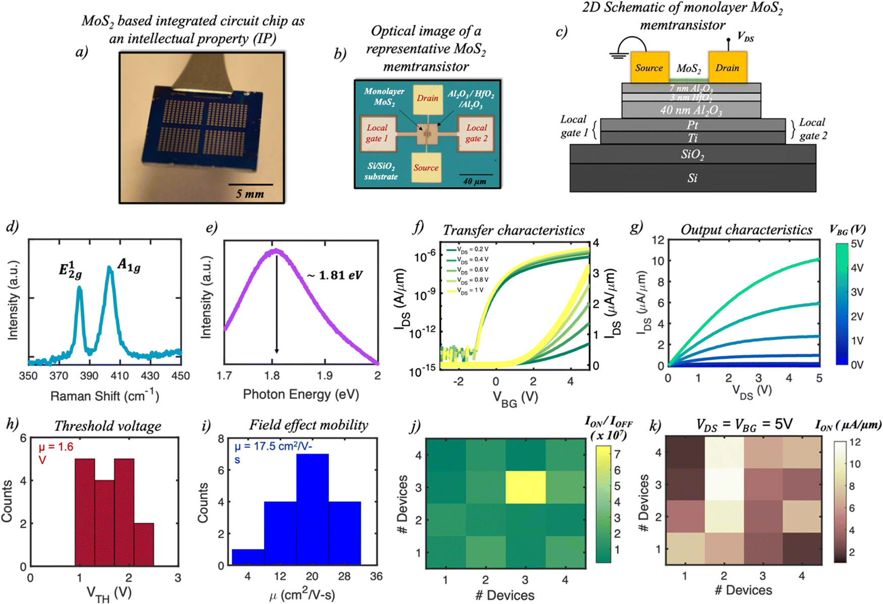 | ||
| Fig. 1 Monolayer MoS2 characterization and memtransistor fabrication: (a) An optical image of a MoS2-based integrated intellectual property (IP) comprising several logic circuits such as NAND, NOR, AND, and a three-stage inverter (TSI) module. (b) An optical image along with a corresponding (c) 2D schematic of a representative individual MoS2-memtransistor. The device structure comprises Platinum/Titanium (Pt/Ti) local gates, a 7 nm Alumina (Al2O3) tunnelling layer, a 3 nm Hafnia (HfO2) charge-trapping layer, and a 40 nm Al2O3 blocking layer as the gate dielectric stack with Ni/Au (40/30 nm) as the source and drain contact pads. All the memtransistors have a channel length (L) of 1 μm, a channel width (W) of 5 μm, and two local gates from either side for better accessibility. (d) Raman and (e) photoluminescence (PL) spectra, respectively, obtained from a representative MoS2 film where the characteristic in-plane E12g mode and out-of-plane A1g mode were observed at 385 cm-1 and 403 cm-1, respectively, with the PL peak at 1.83 eV. (f) Transfer characteristics of a representative MoS2 memtransistor in the logarithmic and linear scales where the source-to-drain current (IDS) is plotted with respect to the local back-gate voltage (VBG) and measured at different source-to-drain (VDS) biases. A clear n-type dominated carrier transport is observed. (g) A plot of the output characteristics where IDS is plotted against VDS as a function of different VBG biases with excellent ION values of 10 μA μm−1 for VDS = 5 V at VBG = 5 V. Histogram plots for the extracted (h) threshold voltage (VTH) at an iso-current of 100 nA μm−1 with a mean of 1.6 V and (i) peak electric field mobility (μn) extracted using the transconductance method with a mean of 17.5 cm2 V-1 s-1 along with the colormap plots of (j) ION/IOFF ratio and (k) ION values at a VDS = VBG = 5 V for a population of 16 MoS2 memtransistors; these results further confirm the high quality of our channel material. | ||
Fig. 1d and e, respectively, show the Raman and the photoluminescence (PL) spectra obtained from a representative MoS2 film where the characteristic in-plane E12g mode and out-of-plane A1g mode were observed at 385 cm-1 and 403 cm-1, respectively, and the PL peak was found to be at 1.81 eV; these results are consistent with a monolayer film. Fig. 1f shows the transfer characteristics of a representative MoS2 memtransistor where the source-to-drain current (IDS) is plotted in the linear and logarithmic scales with respect to the local back-gate voltage (VBG) when measured at different source-to-drain biases (VDS). A clear n-type dominated carrier transport is observed due to the pinning of the metal Fermi level near the conduction band facilitating enhanced electron injection.60,61 In addition, an excellent ON/OFF current ratio of ∼107 and a subthreshold slope (SS) of ∼350 mV per decade obtained over three orders of magnitude change in IDS are also observed. The deviation of the SS from the ideal value of 60 mV per dec can be attributed to the presence of interface traps. Next, the output characteristics (Fig. 1g) where IDS is plotted against VDS as a function of different VBG also show excellent ION values of 10 μA μm−1 for VDS = 5 V at VBG = 5 V. Note that further enhancement in the device characteristics can be accomplished through the optimization of metal contacts, as well as scaling the oxide thickness and the channel length62
The device-to-device (D2D) variation was also examined due to our intention to fabricate ICs involving multiple memtransistors. Fig. 1h and i show the histogram plots of the obtained threshold voltage (VTH) at an iso-current of 100 nA μm-1 and the peak electric field mobility (μn) obtained from the trans-conductance 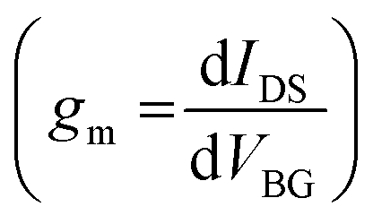 method, respectively, with the corresponding mean values of 1.5 V and 17.5 cm2 V-1 s-1 for 16 different MoS2 memtransistors. Fig. 1j and k show the colormaps of the on/off ratio and ION measured at VDS = 5 V and VBG = 5 V for the same devices. These results confirm the high quality and uniform growth of MoS2, which is critical for successful realization of memtransistor-based ICs. ESI† S1 shows D2D variation across the transfer characteristics and linear VTH obtained for all 16 MoS2 memtransistors. Although a deterrent, these variations are often unavoidable due to factors such as growth and transfer-related defects, adsorbed water molecules, and resist residues originating from the fabrication process. However, they do not hinder or limit our ability as an adversary to insert HTs into chip designs.
Basis of in-memory computing inspired hardware Trojans (HTs) in MoS2 intellectual property (IP)
In this section, we demonstrate the non-volatile electrical programmability of our 2D memtransistors as the basis for inserting HTs into the IP core. Fig. 2a shows the pre-Trojan baseline transfer characteristics of a representative memtransistor in both the logarithmic and linear scales with expected carrier transport behavior. Trojans are inserted by applying a voltage pulse to the local gate of the MoS2 memtransistor which results in an altered device characteristic. Fig. 2b and c, respectively, show the transfer characteristics (logarithmic and linear scales) for the same representative memtransistor post Trojan insertion. It can be clearly seen that the application of a negative voltage pulse shifts the device threshold voltage (VTH) towards a more negative value, thereby making it less resistive (more conductive), whereas a positive voltage pulse shifts VTH towards a more positive value, making it more resistive (less conductive). This shift is attributed to the tunnelling of charge carriers across the 7 nm Al2O3 into the HfO2 charge-trapping layer. The ability to draw the carriers into the FG is enabled by Fowler-Nordheim tunnelling63 applying a large negative/positive voltage pulse to the CG facilitates the tunnelling of electrons/holes, respectively, through the thin tunneling oxide layer (7 nm Al2O3) and into the FG, thereby screening the electric field and accounting for the observed VTH shifts. ESI† S2 shows the band diagram associated with the described tunnelling phenomenon. Note that a similar charge trapping phenomenon with a different gate stack has also been extensively discussed in our earlier reports.30,53,54 While similar VTH shifts are also observed due to the long-term drifts of the device characteristics as a result of bias-temperature instability (BTI),64 the slow and often prolonged nature of the process renders it infeasible for timely insertion of HTs from an adversary's perspective. Due to their distinct effect on memtransistor characteristics, we have defined the negative voltage pulse as low resistance Trojan voltage (VLRT) and the positive voltage pulse as high resistance Trojan voltage (VHRT). We applied a −10 V and a 15 V bias pulse as VLRT and VHRT, respectively, with a pulse width (τw) of 100 μs each, which remains constant for all subsequent discussions. Note that, for our demonstration, VLRT and VHRT are defined as trigger mechanisms whereas the affected logic designs are defined as the payload. Also note that similar resistive memories have also been demonstrated earlier for memristive65,66 and oxide nanosheet materials.67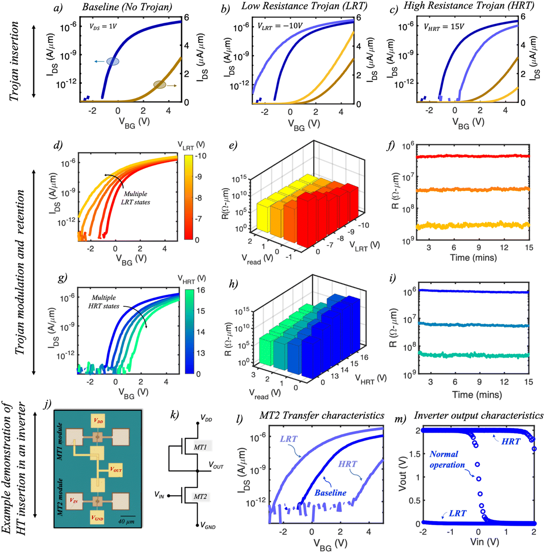 | ||
| Fig. 2 Basis of non-von-Neumann-based hardware Trojans (HTs) in monolayer MoS2 memtransistors: (a) Transfer characteristics of a representative memtransistor in three different scenarios: (a) no Trojan, (b) post low resistance Trojan (LRT) insertion and (c) post high resistance Trojan (HRT) insertion. (d) Transfer characteristics of a representative MoS2 memtransistor for different VLRT magnitudes ranging from −7 V to −10 V and their (e) corresponding resistance values extracted at different Vread = VBG values. (f) Retention plot for three different LRT states which were found to be stable over 15 minutes. (g) Transfer characteristics of the same MoS2 memtransistor for different VHRT magnitudes ranging from 13 V to 16 V and their (h) corresponding resistance values extracted at different Vread = VBG. (i) Retention plot for three different HRT states which were also stable over 15 minutes. (j) An optical image and a (k) circuit diagram of an inverter, fabricated using a depletion-mode (D-mode) memtransistor (MT1) and an enhancement-mode (E-mode) memtransistor (MT2). (l) Transfer characteristics of MT2, measured pre-Trojan (baseline), post VLRT = −10 V (LRT) insertion, and post VHRT = 15 V (HRT) insertion. (m) Inverter output characteristics showing normal operation along with post LRT and HRT operations with clear performance degradation. | ||
It is also interesting to note that our MoS2 memtransistors offer the unique capability of modulating both the low resistance Trojan (LRT) and high resistance Trojan (HRT) states as a function of the applied magnitude of VLRT and VHRT, respectively. Although the overall aim is to corrupt or provide faulty logic at the output, the modulation becomes important from a D2D variation point of view which is generally observed across a large population of 2D-memtransistors and can necessitate application of higher or even lower magnitudes of VLRT and VHRT. Fig. 2d shows the transfer characteristics of a representative MoS2 memtransistor for different VLRT magnitudes ranging from −7 V to −10 V and their corresponding resistance values (Fig. 2e) obtained at different Vread = VBG values. Two observations can be made from these plots. First, for any given VLRT, the values of LRT states decrease as Vread increases. This is expected since the Vread values gradually shift from the sub-threshold region towards the ON state. Second, the LRT values also decrease as a function of the magnitude of VLRT at any given Vread value. This phenomenon can be attributed to the higher number of electrons tunnelling into the FG with increasing VLRT which results in a larger negative VTH shift. The LRT states were found to be very retentive (Fig. 2f) when measured for over 15 minutes. Similarly, Fig. 2g and h, respectively, show the transfer characteristics for different VHRT magnitudes ranging from 13 V to 16 V and their corresponding resistance values (Fig. 2h) obtained at different Vread = VBG. While following the similar trend as a function of Vread values, the HRT states show the converse effect with increasing VHRT magnitude. Once again, this is expected due to the larger positive VTH shift with increasing VHRT magnitude, which would suggest a larger amount of electron tunnelling out of the FG. Note that this ability to electrostatically alter the channel conductance through application of VBG, which acts as the third terminal, is what differentiates our memtransistor architecture from other similar prototypes such as metal–insulator–metal (MIM) structures or memristors, which are simple two terminal devices offering limited tunability and electrostatic control. Like the LRT states, the HRT states were also found to be retentive (Fig. 2i).
Next, as an example demonstration, we successfully inserted a Trojan into an inverter module and corrupted its functionality. An inverter is one of the most fundamental and well-known logic circuits whose output reflects the opposite logic-level of its input. Fig. 2j and k, respectively, show an optical image and a circuit diagram of the inverter, which was using a depletion-mode (D-mode) memtransistor (MT1) and an enhancement-mode (E-mode) memtransistor (MT2). Note that the gate and source terminals of MT1 in our design are shorted in order for it to act as an n-type depletion load in the absence of a p-type memtransistor. Fig. 2l shows the transfer characteristics of MT2, measured as-fabricated (baseline), post VLRT = −10 V (LRT) application, and post VHRT = 15 V (HRT) application; Fig. 2m shows the inverter output characteristics considering all three scenarios for a representative applied voltage (VDD) of 2 V. For the baseline state, application of Vin = 0 V (logic state ‘0’) to the gate of MT2 results in Vout = VDD = 2 V since, at VBG = 0 V, MT2 is highly resistive compared to MT1 (logic state ‘1’). Conversely, applying Vin = 2 V (logic state ‘1’) clamps the Vout to 0 V (logic state ‘0’) since MT2 is now less resistive than MT1 at VBG = 2 V. However, post HT insertion, faulty inverter behavior is observed. For both the LRT and the HRT states, respectively, Vout always remains clamped to 0 V and 2 V with no apparent transition or switching point. This is because MT2 now remains either always “ON” (the LRT state) or always ‘OFF’ (the HRT state) compared to MT1. Interestingly, despite the HRT state of MT2, the inverter exhibits normal operation for VDD = 5 V (ESI† S3). Therefore, assuming it continually functions at this higher supply voltage, the presence of HTs remains hidden at VDD = 2 V (rare node). It must be noted that, for the LRT state, Vout always remains clamped to 0 V regardless of the VDD value. We would also like to point out that for this particular case and the subsequent discussions, the adversary attack model relies on accelerated aging of the IC. Since HT insertion techniques continue to evolve, there is no guarantee that every attack mechanism is addressed. Therefore, run-time monitors are often deployed in ICs as the last line of defense, with the an aim to switch the IC operating conditions to a safe mode if an HT is detected.68,69 For our MoS2 IC, this safe mode can only be enabled through higher VDD operations which inevitably lead to higher power consumption and energy dissipation, both of which are detrimental for any circuit/chip operation in terms of its operational lifetime.
Demonstration of in-memory HTs in a three-stage inverter (TSI) circuit
Continuing from the discussion above, here we exploit the degradation observed in the SS of a 2D memtransistor in a cascaded three-stage inverter (TSI) circuit module as a form of HT. Fig. 3a and b, respectively, show the optical image and the corresponding circuit schematic of our TSI design which consists of three inverters connected in series; the Vout from a single inverter is fed as the Vin to the next stage inverter. Fig. 3c shows the process flow of HT insertion, which begins by first measuring the baseline transfer characteristics of the MT2 from stage 1. Thereafter, the HT is inserted in two steps. First, a VHRT pulse of magnitude 15 V is applied to one of the local gates of MT2, the effect of which can be seen through a large positive VTH shift in the device characteristics. This is followed by the application of a large VLRT pulse of −12 V in an attempt to bring the device back to its baseline state. Interestingly, the device never fully recovers, the evidence of which can be clearly seen through the SS degradation from 243 mV per dec to 420 mV per dec. In order support this finding, we repeated the experiment with three different individual 2D memtransistors and analyzed their SS both before and after HT insertion with similar results as shown in the 3D bar plot in Fig. 3d. This degradation in SS can be attributed to the development of permanent damage in the underlying Al2O3 oxide due to repeated high magnitude voltage stressing of the devices. ESI† S4 shows the transfer characteristics for the three memtransistors pre- and post-HT insertion. | ||
| Fig. 3 Demonstration of in-memory HTs in a cascaded three-stage inverter (TSI) circuit: (a) An optical image and the (b) corresponding circuit schematic of our TSI design consisting of three inverters connected in-series where the Vout from a single inverter is fed as the Vin to the next stage inverter. (c) Evolution of the degradation in subthreshold slope (SS) of MT2 through application of a VHRT pulse of 15 V followed by a VLRT pulse of −12 V to bring the device back to its baseline state. Both the voltage pulses are applied to one of the local gates of MT2 from stage 1. (d) A 3D bar plot showing similar SS degradation for four separate 2D memtransistors which is attributed to permanent damage caused to the underlying Al2O3 oxide due to repeated high magnitude voltage stressing of the devices. Inverter output characteristics plots for (e) pre-HT and (f) post-HT clearly showing the deterioration of the overall gain as a result of HT insertion which is further confirmed by (g) analyzing the maximum gain as shown using the 3D bar plot. (h) A 3D bar plot of the extracted Vm which clearly shows a significant positive Vm shift as compared to the original pre-HT state of the inverters. | ||
Next, Fig. 3e and f, respectively, show the inverter output characteristics plots for all the three stages of the cascaded TSI both before and after the HT insertion. The degradation in the gain is clearly visible from the plots. Note that the inverter gain, defined as the slope of the inverter characteristics, i.e.,  , increases with the number of stages prior to HT insertion. The overall reduction in the maximum gain for all the three stages post-Trojan insertion, as shown using the 3D bar plot in Fig. 3g, is attributed to the degraded SS of MT2. This is because a steeper SS would signify a more rapid change in the corresponding current values as a function of the applied gate-bias, which would, in turn, imply a more abrupt transition between the two logic levels, i.e., VDD = 2 V and 0 V. In addition to the SS and the corresponding gain degradation, we also evaluated the change in the switching voltage (Vm), which is defined as the magnitude of Vin for which Vout reaches VDD/2, for all the inverters by applying a single VHRT pulse of 15 V and length τw = 100 μs to MT2. Fig. 3h shows the 3D bar plot of the extracted Vm which clearly shows a significant positive Vm shift as compared to the original pre-HT state of the inverters. ESI† S5 shows the corresponding output inverter plots following VHRT application to MT2 for all the stages.
Demonstration of in-memory HTs in a NOR logic design
Fig. 4a and b, respectively, show the optical image and the circuit schematic of a NOR gate fabricated using our 2D memtransistors. Note that in the optical image our design is shown within the demarcated white dashed line. A NOR is the negation of the logical OR operation and is also a universal logic gate which operates as per the truth table shown in Fig. 4c. In our design, we have combined two E-mode memtransistors, MT1 and MT2, with a D-mode memtransistor, MT3. Prior to HT insertion, we first measure the baseline transfer characteristics of both MT1 and MT2 as shown in Fig. 4d and e, respectively. This is followed by measuring the output characteristics of the NOR gate under normal operating conditions for all possible input combinations. As shown in Fig. 4f, Vout = VDD = 2 V (logic ‘1’) only when both Vin1 and Vin2 are at logic ‘0’. This behavior can be attributed to the highly resistive state of both MT1 and MT2 at VBG = 0 V, which effectively clamps the Vout to the VDD supply. For all the other input combinations, Vout always remains at logic ‘0’ since, at VBG = 2 V, either MT1 or MT2, or both, remain at a lower resistance state than MT3, thereby clamping Vout to VGND. These results are in agreement with the truth table shown earlier. Note that to ensure correct logical operations (without HTs), the E-mode memtransistors must initially remain OFF at VBG = 0 V. Therefore, any memtransistor which conducts at this VBG as a result of the D2D variation must be biased properly through application of a programming pulse.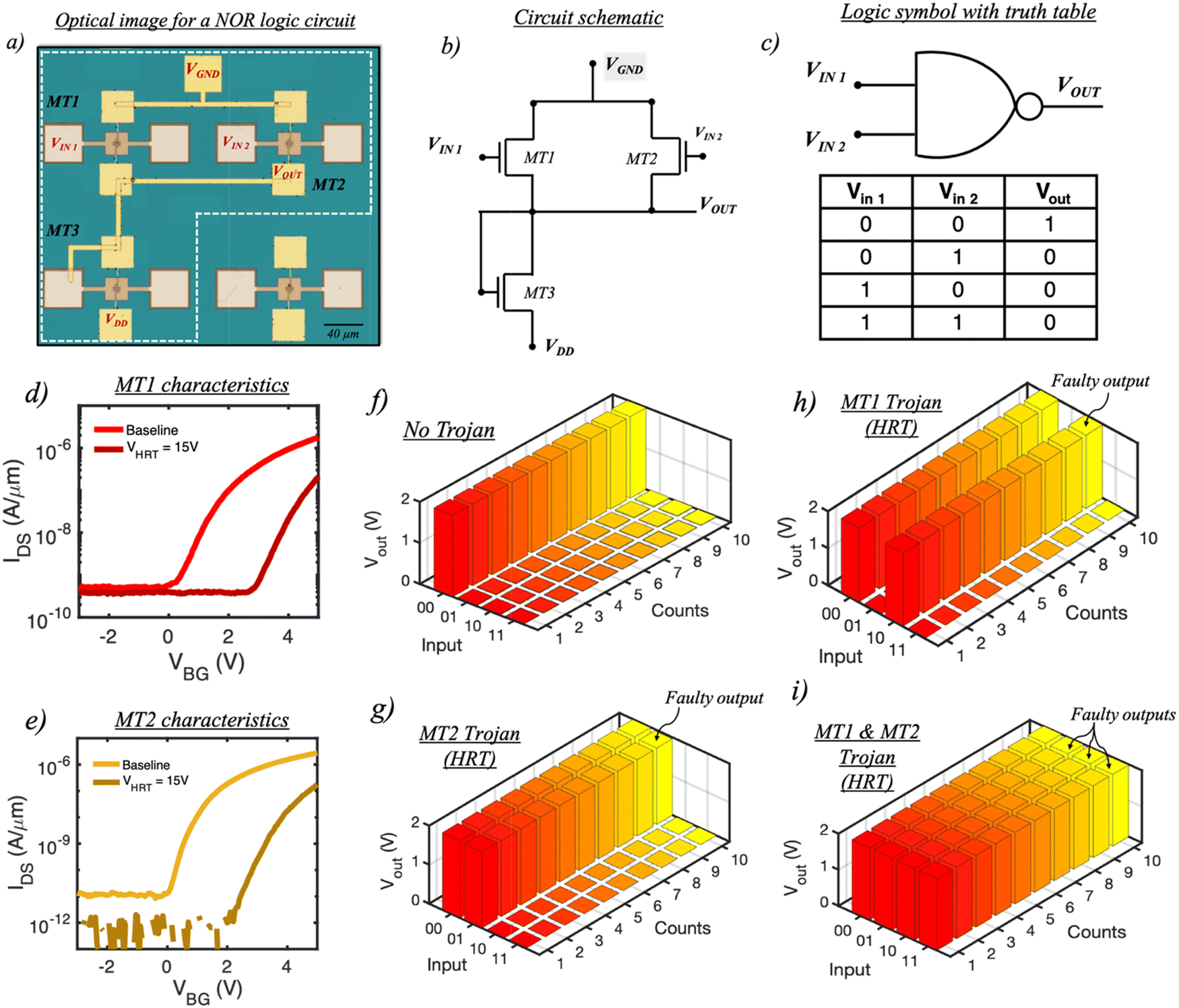 | ||
| Fig. 4 Demonstration of in-memory HTs in a NOR logic design: (a) An optical image and the (b) circuit schematic of a NOR gate fabricated using two E-mode memtransistors, MT1 and MT2, with a D-mode memtransistor, MT3, along with its (c) logic symbol and truth table. Note that the NOR design is shown within the demarcated white dashed line in the optical image. Transfer characteristics of (d) MT1 and (e) MT2 memtransistors for both the baseline and post VHRT = 15 V HT insertion. Output characteristics of the NOR gate for all the possible input combinations under (f) normal operating conditions, which are in agreement with the truth table, (g) post MT2 HT insertion resulting in a corrupt Vout = VDD = 2 V (logic ‘1’) value for the specific input combination of ‘01’, (h) post MT1 HT insertion resulting in a corrupt Vout = VDD = 2 V (logic ‘1’) value for the specific input combination of ‘10’, and (i) post MT1 and MT2 HT insertion resulting in a totally corrupt NOR logical operation where, regardless of any input combinations, Vout = VDD = 2 V. | ||
Next, we demonstrate our capability as an adversary to produce corrupt Vout values for specific combinations of Vin1 and Vin2. For example, it is possible to engineer a faulty Vout value for the input combination ‘01’ by simply inserting an HT in MT2 by applying a VHRT pulse of 15 V while keeping MT1 in its baseline state (refer to Fig. 4d and e). In this case, MT2 remains in an HRT state when VBG = 2 V; therefore, for an input combination ‘01’, both MT1 and MT2 now act as an open circuit path which ensures Vout = VDD = 2 V (logic ‘1’) as seen in Fig. 4g. Following a similar logic, applying a VHRT pulse of 15 V to MT1 while keeping MT2 in its baseline state ensures Vout = VDD = 2 V for the input combination ‘10’ as seen in Fig. 4h. However, in this case, MT1 remains in an HRT state when VBG = 2 V. Finally, applying a VHRT pulse of 15 V to both MT1 and MT2 results in a totally corrupt NOR logical operation where, regardless of any input combinations, Vout = VDD = 2 V as shown in Fig. 4i, which is due to the HRT state of both MT1 and MT2 at VBG = 2 V. Once again, when the VDD is scaled to 5 V, the NOR gate resumes its normal functionality, as shown in ESI† S6, while the Trojan remains hidden at a lower VDD supply of 2 V (rare node).
Demonstration of in-memory HTs in a NAND logic design
Fig. 5a and b, respectively, show the optical image and the circuit schematic of a NAND gate fabricated using two E-mode memtransistors, MT1 and MT2, that are in series with one D-mode memtransistor, MT3. Another universal gate, a NAND produces low output (logic ‘0’) only when all of its inputs are high (logic ‘1’). Therefore, its output is complemented to that of an AND gate as shown in the truth table in Fig. 5c. Moving along similar lines, we first begin with measuring the baseline transfer characteristics of both MT1 and MT2 as shown in Fig. 5d and e, respectively, followed by the output characteristics (Fig. 5f) prior to HT insertion. Clearly, the expected NAND logic functionality is observed where Vout = VDD = 2 V (logic ‘1’) for the input combinations of ‘00’,’01’, and ‘10’ due to the high resistive state of both MT1 and/or MT2 compared to MT3. However, for the input combination ‘11’, Vout = VGND = 0 V (logic ‘0’) since now both MT1 and MT2 become more conductive than MT3. Note that this is in line with the truth table shown earlier. The HT is then inserted by applying a VHRT pulse of 15 V (τw = 100 μs) to the local gate of MT1, which results in the positive shift in the MT1 device characteristics. On remeasuring the NAND, we now see a faulty Vout for the input combination of ‘11’. This behavior is attributed to the HRT state of MT1 which will now always clamp the Vout to VDD = 2 V. Note that, unlike the NOR logic, our NAND logic design requires HT insertion in only one of the two E-mode memtransistors (MT1 or MT2). Once again, despite the presence of HT at the rare node (VDD = 2 V), normal NAND functionality is observed for VDD = 5 V as shown in ESI† S7.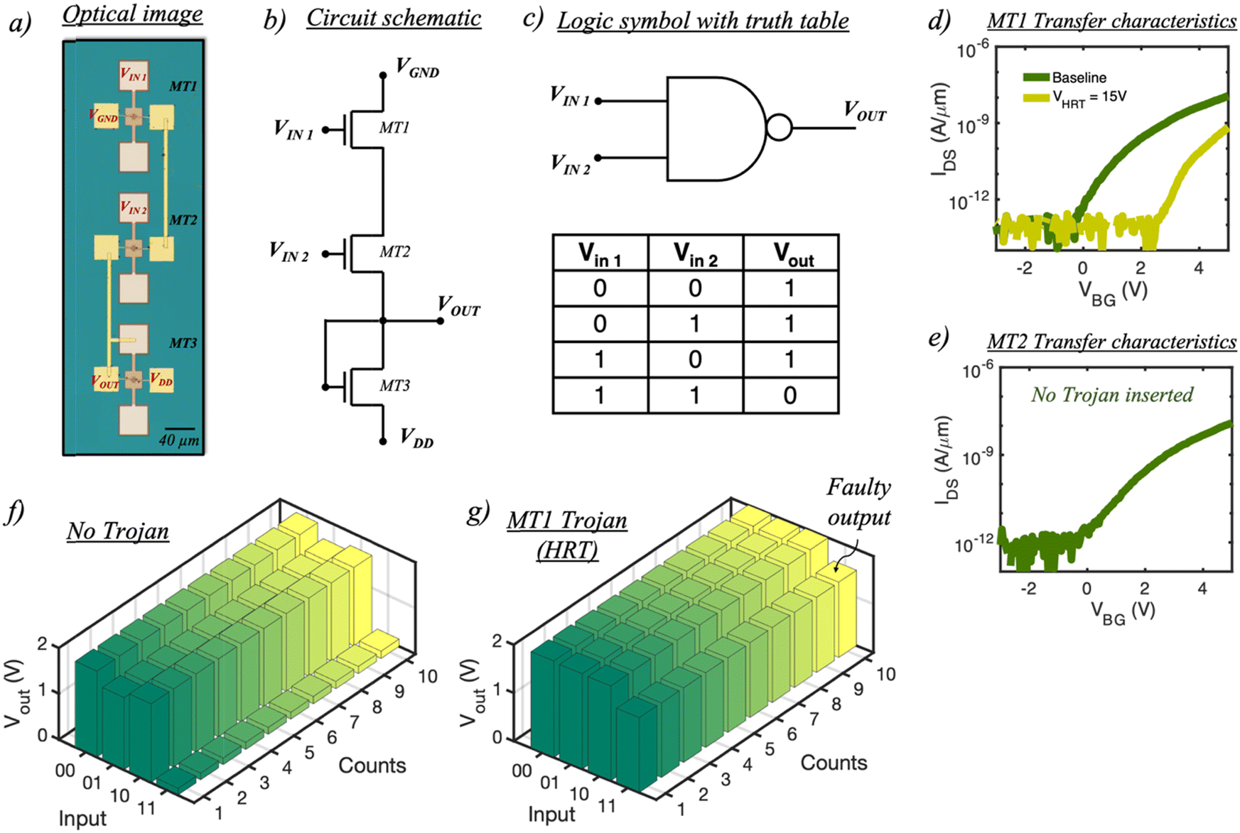 | ||
| Fig. 5 Demonstration of in-memory HTs in a NAND logic design: (a) An optical image and the (b) circuit schematic of a NAND gate fabricated using two E-mode memtransistors, MT1 and MT2, with a D-mode memtransistor, MT3, along with its (c) logic symbol and truth table. Transfer characteristics of (d) MT1 for both the baseline and post VHRT = 15 V HT insertion along with the baseline transfer characteristics of (e) MT2. Note that for our NAND logic design only one of the two memtransistors require insertion of HT. Output characteristics of the NAND gate for all the possible input combinations under (f) normal operating conditions, which are in agreement with the truth table, and (g) post MT1 HT insertion, resulting in a corrupt Vout = VDD = 2 V (logic ‘1’) value for the specific input combination of ‘11’. | ||
Demonstration of in-memory HTs in an AND logic design
Finally, Fig. 6a and b, respectively, show the optical image and the circuit schematic of an AND gate with a similar memtransistor configuration to that of a NAND gate except for the switching of the VDD and VGND polarities along with the shorting of the gate terminal of MT3 to VGND. The AND logic can be summarized using the truth table shown in Fig. 6c where Vout remains high (logic 1’) only when both Vin1 and Vin2 are high. Fig. 6d and e, respectively, show the baseline transfer characteristics of MT1 and MT2. Prior to HT insertion, a normal AND logic functionality is observed as shown in Fig. 6f where, for the input combinations of ‘00’, ‘01’, or ‘10’, Vout = VGND = 0 V (logic ‘0’) since either one or both MT1 and MT2 are more resistive than MT3. However, for the input ‘11’, MT1 and MT2 become more conductive than MT3, which clamps Vout to VDD = 2 V (logic ‘1’). Next, the HT is inserted by applying a VLRT pulse of −15 V (τw = 100 μs) to both MT1 and MT2, resulting in a negative VTH shift as seen in Fig. 6d and e. The effect of inserting this HT can be understood by once again observing the output characteristics, as shown in Fig. 6g where now regardless of the input combination, Vout = VDD = 2 V (logic ‘1’) since both MT1 and MT2 are in the LRT state and offer a more conductive path compared to MT3.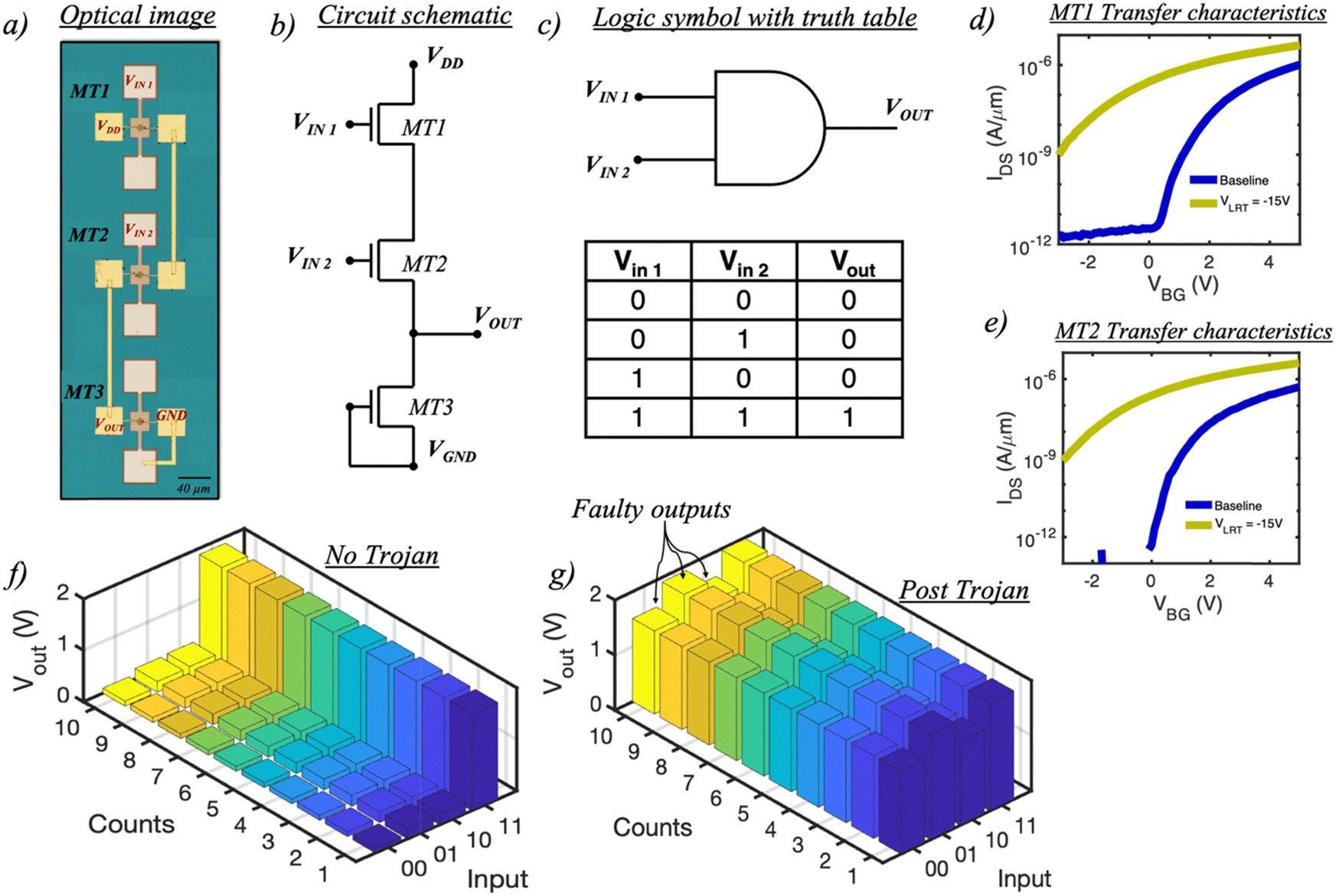 | ||
| Fig. 6 Demonstration of in-memory HTs in an AND logic design: (a) An optical image and the (b) circuit schematic of a NAND gate fabricated using two E-mode memtransistors, MT1 and MT2, with a D-mode memtransistoor, MT3, along with its (c) logic symbol and truth table. Transfer characteristics of (d) MT1 and (e) MT2 at both the baseline and post VLRT =−15 V HT insertion. Note that for our AND logic design both memtransistors require insertion of HT. Output characteristics of the AND gate for all possible input combinations under (f) normal operating conditions where, for the input combinations of ‘00’, ‘01’, or ‘10’, Vout = VGND = 0 V (logic ‘0’) since either one or both MT1 and MT2 are more resistive than MT3 and (g) post MT1 and MT2 HT insertion where, regardless of the input combination, Vout = VDD = 2 V (logic ‘1’) since both MT1 and MT2 are now in the LRT state and offer a more conductive path compared to MT3. | ||
Enabling complete failure of logic designs with in-memory HTs
In addition to corrupting the circuit outputs for a particular set of input combinations, it is also possible for an adversary to engineer a complete failure or malfunction of the logic designs using the described in-memory HT insertion technique. In this context, we define a complete logic failure as a scenario where Vout always remains low (logic ‘0’) regardless of the input combination. In other words, the chip becomes completely non-functional. Fig. 7a and c, respectively, show the transfer characteristics of MT1 and MT2 in the NOR, NAND, and AND logic designs measured for both baseline and post-HT configurations. Note that in each case, the type of HT inserted (VLRT or VHRT) would be different. For example, in order to make the NOR and NAND logic malfunction, a VLRT pulse of −15 V (τw = 100 μs) is applied to both MT1 and MT2, whereas the AND logic malfunctioning requires an application of a VHRT pulse of 15 V (τw = 100 μs). On observing their respective output characteristics, as shown in Fig. 7d–f, it is evident that each logic design has malfunctioned since Vout = VGND = 0 V (logic ‘0’) for all input combinations. In the case of the NOR and NAND logic design, this can be attributed to the LRT state of both MT1 and MT2, whereas for the AND logic design, both MT1 and MT2 are in the HRT state compared to MT3.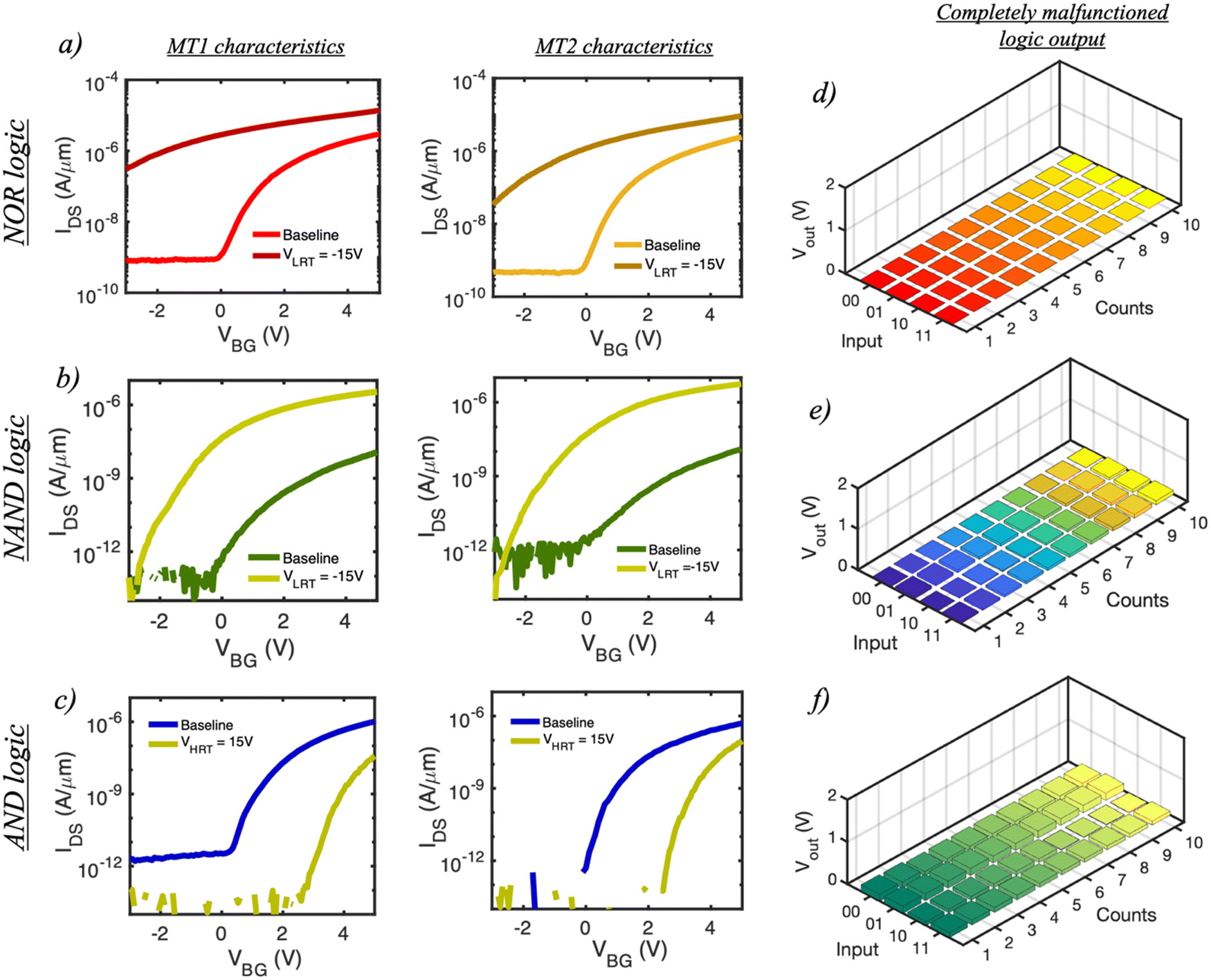 | ||
| Fig. 7 Enabling complete failure of logic designs with in-memory HT: Transfer characteristics of MT1 and MT2 measured for the (a) NOR, (b) NAND, and (c) AND logic designs under both baseline and post-HT configurations. (d–f) Malfunctioned output characteristics for each respective logic design since Vout = VGND = 0 V (logic ‘0’) regardless of the input combinations. In case of the NOR and NAND logic design, this can be attributed to the LRT state of both MT1 and MT2, whereas for the AND logic design, both MT1 and MT2 are in the HRT state compared to MT3. It must be noted the type of HT inserted (VLRT or VHRT) is different for each individual design. For example, in order to make the NOR and NAND logic malfunction, a VLRT pulse of −15 V (τw = 100 μs) is applied to both MT1 and MT2, whereas the AND logic malfunctioning requires an application of a VHRT pulse of −15 V (τw = 100 μs). | ||
Trojan lifetime and detection countermeasures avoidance
From the above discussions, it is abundantly clear that from an adversary's perspective, the ultimate goal is to enable an HT attack mechanism which is precise and stealthy, with a small footprint such that it is capable of evading detection countermeasures.70 For our in-memory HT demonstration, we have achieved all of the aforementioned requirements. First, despite the VTH shifts observed as a result of VLRT or VHRT application, the presence of the HT is obscured since the electrical measurements of the affected individual 2D memtransistor do not offer any additional information. Although it can be argued that the device performance parameters such as SS and ION values degrade slightly, these parameters are more likely to be attributed to fabrication constraints and D2D variation related factors. Furthermore, our HT injection scheme also fulfills the criteria of having a small footprint since the HT can be triggered (VLRT and VHRT application) without requiring any additional peripheral components within the design.Additionally, from our point of view as an adversary, a good retention of both LRT and HRT states is desirable for delivering the payload. Therefore, we examined the extended retention of our memtransistors for two different states over a total of 104 seconds, or ∼3 hours (ESI† S8). Although the two memory states will eventually converge after ∼15 hours, as evident through the slow collapse of the memory ratio (MR) due to an exponential decay, an adversary can employ this attribute to cause catastrophic malfunctions and failures in critical technological infrastructure such as military equipment and aircraft navigation and still evade detection since the presence of HTs can only be confirmed if the black box retrieved from the failed equipment is analyzed within the MR retention time frame. As soon as the MR window vanishes and the HT disappears, no evidence of a Trojan ever being inserted can be recovered. Note that this decay might seem counterintuitive as far as deliberately aging or causing a total logic malfunction of the IC is concerned. This is because both of these adversarial intentions would ideally require the HT to be present within an IC at all times. However, in the present day's era of stiff market competition and time-to-market demands requiring increased productivity and shorter design time, any degradation or malfunction observed within this global supply chain will likely result in the affected IP being discarded completely, leading to severe monetary loss in addition to reputational dissolvement for the involved parties.
Conclusions
In conclusion, we have exploited and exposed the vulnerability of the in-memory computing architecture to insert hardware Trojans (HTs) within basic digital logic designs such as AND, NAND, NOR and NOT gates fabricated using monolayer MoS2 memtransistors. In addition, we have also exploited the degradation in subthreshold slope (SS) due to the presence of HTs to drastically compromise the performance of a cascaded three stage inverter (TSI). The HT is inserted by applying an electrical voltage pulse (VHRT or VLRT) to the local gate of our memtransistor devices, programming them into either HRT or LRT states which significantly corrupts and even causes complete logic malfunction within our circuit. This ability to enable both the LRT and HRT states as a function of the applied magnitude of VLRT and VHRT can be attributed to the tunnelling of charge carriers across the 7 nm Al2O3 into the HfO2 charge-trapping layer due to the Fowler Nordheim tunneling process. Moreover, the Trojan remains hidden within the rare node during the normal operation of the logic designs at a higher VDD = 5 V and only gets activated when the supply voltage is scaled down (VDD = 2 V). These results are not just limited to 2D-based technologies but are applicable to any state-of-the-art in-memory computing architecture. Our approach in the role of an adversary offers a rather unconventional, uncomfortable, and eye-opening insight into the vulnerabilities of in-memory computing in today's highly complex and globalized IP supply chain system, which can be exploited in unimaginable ways to compromise the security, reliability, and even the lifetime of electronic components.Methods
Large area monolayer MoS2 film growth
The metal–organic chemical vapor deposition (MOCVD) technique was used to deposit monolayer MoS2 on an epi-ready 2” c-sapphire substrate. A cold-wall horizontal reactor with an inductively heated graphite susceptor and a wafer rotation was utilized to assist in achieving a uniform monolayer deposition.71 Molybdenum hexacarbonyl (Mo (CO)6) and hydrogen sulfide (H2S) were used as precursors. Prior to the material growth, the substrate was heated to 1000 °C in H2 and maintained for 10 min. (Mo (CO)6). For the growth process, Mo (CO)6 was maintained at 10 °C and 650 Torr in a stainless-steel bubbler to deliver 1.1 × 10⁻³ sccm of the metal precursor along with 400 sccm of H2S. The monolayer MoS2 deposition was achieved in 18 min at 950 °C in 50 Torr H2 ambient. Following the growth of the MoS2 film, the substrate was cooled down to 300 °C in H2S to prevent its decomposition. More details can be found in our earlier work.51,72,73Fabrication of local back-gate islands
To define the features with local gate island configuration, the 285 nm SiO2 on the p++-Si substrate (commercially purchased) was first spin-coated with a bilayer poly(methyl methacrylate) or PMMA resist in a two-step process and subsequently baked at 185 °C and 95 °C for 60 s and 90 s, respectively. Next, an EBPG 5200 Vistec Electron Beam Lithography tool was used to pattern the individual islands. The exposed resist was developed using a 4-methyl-2-pentanone (MIBK) and 2-propanol (IPA) solution in a 1![[thin space (1/6-em)]](https://www.rsc.org/images/entities/char_2009.gif) :1 mixture. Following a sputter cleaning of the substrate with O2 plasma, the local-gate electrodes comprising Ti/Pt (20/50 nm) layers were deposited using a Temescal e-beam evaporator. This was followed by lifting off the excess metal in a cold acetone bath. Next, the atomic layer deposition (ALD) process was performed to grow the Al2O3/HfO2/Al2O3 layers. Subsequently, a Heidelberg Maskless Aligner (MLA 150) was utilized to pattern and subsequently define the access points to the local back-gate electrodes. The excess oxide in the exposed areas was subsequently removed using BCl3 based reactive ion etch (RIE) chemistry.
:1 mixture. Following a sputter cleaning of the substrate with O2 plasma, the local-gate electrodes comprising Ti/Pt (20/50 nm) layers were deposited using a Temescal e-beam evaporator. This was followed by lifting off the excess metal in a cold acetone bath. Next, the atomic layer deposition (ALD) process was performed to grow the Al2O3/HfO2/Al2O3 layers. Subsequently, a Heidelberg Maskless Aligner (MLA 150) was utilized to pattern and subsequently define the access points to the local back-gate electrodes. The excess oxide in the exposed areas was subsequently removed using BCl3 based reactive ion etch (RIE) chemistry.
MoS2 film transfer to local back-gate islands
In order to fabricate the MoS2 memtransistors, transfer of monolayer MoS2 films from the growth substrate (sapphire) to the application substrate (SiO2/p++-Si) with local back-gate islands is the first step. This was achieved using a polymethyl-methacrylate (PMMA) assisted wet transfer process. First, the sapphire substrate with the monolayer film was spin-coated with PMMA and left idle for 24 hours in order to ensure good adhesion between PMMA and MoS2. Next, the corners of the spin-coated film were lightly scratched with a razor blade followed by its immersion in a 2 M NaOH solution at 90 °C. Owing to the hydrophilic and hydrophobic nature of sapphire and MoS2/PMMA, respectively, NaOH is drawn towards the substrate/MoS2 interface due to the capillary action thereby separating the PMMA/MoS2 stack from the sapphire substrate. Using a clean glass slide, the separated film is then carefully taken out from the NaOH solution and rinsed in three separate water baths for 15 minutes each before being finally transferred onto the application substrate. Post-transfer, the substrate is baked at 50 °C and 70 °C for 10 min each in order to remove the excess moisture and promote good film adhesion. This ensures a pristine interface. Finally, the PMMA is removed using acetone followed by a final cleanse with IPA.Fabrication of 2D memtransistors
For fabricating MoS2 memtransistors, the substrate with MoS2 on-top was spin-coated with PMMA and baked at 180 °C for 90 s. Electron beam (e-beam) lithography was used to define the features by exposing the resist which was subsequently developed using a 1:1 mixture of 4-methyl-2-pentanone (MIBK) and IPA for 60 seconds and 45 seconds, respectively. The exposed monolayer MoS2 film was etched using a sulfur hexafluoride (SF6) RIE at 5 °C for 30 s followed by an acetone and IPA rinse to remove the e-beam resist. Next, the sample was again spin-coated with methyl methacrylate (MMA) and A3 PMMA resist which was accompanied by E-beam lithography to define the source and drain contacts. The subsequent developing was once again carried out using a 1:1 mixture of MIBK and IPA for the same times as previously described. Finally, nickel/gold (40/30 nm) metal contacts were deposited using e-beam evaporation followed by a lift-off process to remove the evaporated Ni/Au except from the source/drain patterns by immersing the sample in acetone for 30 min followed by IPA for another 30 min.
Multidevice integration
The connections between individual memtransistors were achieved using similar resist, e-beam lithography, and development processes as discussed previously. The interconnect metals Ni/Au (60/30 nm) were deposited using an E-beam evaporator. A greater metal thickness was required compared to the source/drain contacts due to the requirement for a conformal metal coating over/along the sidewalls. Finally, the e-beam resist was removed using a lift-off process with acetone and IPA.Electrical characterization
The electrical measurements for devices and circuits were performed in a Lake Shore CRX-VF probe station in air using a Keysight B1500A parameter analyzer.Data availability
The experimental data generated in this study and codes used to analyze them are available from the corresponding author on reasonable request.Author contributions
A. W. and S. D. conceived the idea, designed the experiments and wrote the manuscript. H. R. fabricated the logic circuits. A. W., and H. R. performed the experiments. A. W., H. R., and S. D. analyzed the data, discussed the results and agreed on their implications. All authors contributed to the preparation of this manuscript.Conflicts of interest
The authors declare no conflicts of interest.Acknowledgements
This work was supported by the National Science Foundation (NSF) through CAREER Award under Grant Number ECCS-2042154. The authors also acknowledge the support from The Pennsylvania State University 2D Crystal Consortium-Materials Innovation Platform (2DCCMIP) for the material growth under NSF cooperative agreement DMR-2039351.References
- L. Yin, R. Cheng, Y. Wen, C. Liu and J. He, Adv. Mater., 2021, 33, 2007081 CrossRef CAS PubMed.
- O. Mutlu, S. Ghose, J. Gómez-Luna and R. Ausavarungnirun, Microprocess. Microsyst., 2019, 67, 28–41 CrossRef.
- D. U. Lee, K. W. Kim, K. W. Kim, H. Kim, J. Y. Kim, Y. J. Park, J. H. Kim, D. S. Kim, H. B. Park and J. W. Shin, IEEE International Solid-State Circuits Conference Digest of Technical Papers (ISSCC), 2014, pp. 432–433.
- J. T. Pawlowski, IEEE Hot chips 23 symposium (HCS), 2011, pp. 1–24.
- S. W. Keckler, W. J. Dally, B. Khailany, M. Garland and D. Glasco, IEEE micro, 2011, 31, 7–17 Search PubMed.
- M. Horowitz, 2014.
- A. Sebastian, M. Le Gallo, R. Khaddam-Aljameh and E. Eleftheriou, Nat. Nanotechnol., 2020, 15, 529–544 CrossRef CAS PubMed.
- G. Indiveri and S.-C. Liu, Proc. IEEE, 2015, 103, 1379–1397 CAS.
- M. Di Ventra and Y. V. Pershin, Nat. Phys., 2013, 9, 200–202 Search PubMed.
- H. Jia, H. Valavi, Y. Tang, J. Zhang and N. Verma, IEEE, J. Solid State Circ., 2020, 55, 2609–2621 Search PubMed.
- Z. Jiang, S. Yin, J.-S. Seo and M. Seok, IEEE, J. Solid State Circ., 2020, 55, 1888–1897 Search PubMed.
- C. Ríos, N. Youngblood, Z. Cheng, M. Le Gallo, W. H. Pernice, C. D. Wright, A. Sebastian and H. Bhaskaran, Sci. Adv., 2019, 5, eaau5759 Search PubMed.
- D. Ielmini and H.-S. P. Wong, Nat. Electron., 2018, 1, 333–343 Search PubMed.
- S. Adee, IEEE Spectrum, 2008, 45, 34–39 Search PubMed.
- J. Kumagai, IEEE Spectrum, 2000, 37, 43–48 Search PubMed.
- R. S. Chakraborty, S. Narasimhan and S. Bhunia, IEEE International high level design validation and test workshop, 2011, pp. 166–171.
- M. Tehranipoor and F. Koushanfar, IEEE Des. Test comput., 2010, 27, 10–25 Search PubMed.
- Y. Alkabani and F. Koushanfar, Proceedings of the 2009 international conference on computer-aided design, 2009, pp. 123–127.
- S. Bhunia, M. S. Hsiao, M. Banga and S. Narasimhan, Proc. IEEE, 2014, 102, 1229–1247 Search PubMed.
- S. Bhunia and M. Tehranipoor, The hardware trojan war, Springer, Cham, Switzerland, 2018 Search PubMed.
- R. S. Chakraborty, I. Saha, A. Palchaudhuri and G. K. Naik, IEEE Des. Test, 2013, 30, 45–54 Search PubMed.
- M. Potkonjak, Proceedings of the 47th Design Automation Conference, 2010, pp. 633–634.
- L. Lin, W. Burleson and C. Paar, IEEE/ACM International Conference on Computer-Aided Design-Digest of Technical Papers, 2009, pp. 117–122.
- S. S. Ali, R. S. Chakraborty, D. Mukhopadhyay and S. Bhunia, Design, Automation & Test in Europe, 2011, pp. 1–4.
- A. Wali, S. Kundu, A. J. Arnold, G. Zhao, K. Basu and S. Das, ACS Nano, 2021, 15, 3453–3467 CrossRef CAS PubMed.
- P. Wu, D. Reis, X. S. Hu and J. Appenzeller, Nat. Electron., 2021, 4, 45–53 CrossRef CAS.
- A. Dodda, S. S. Radhakrishnan, T. F. Schranghamer, D. Buzzell, P. Sengupta and S. Das, Nat. Electron., 2021, 4, 364–374 CrossRef CAS.
- C. Wen, X. Li, T. Zanotti, F. M. Puglisi, Y. Shi, F. Saiz, A. Antidormi, S. Roche, W. Zheng and X. Liang, Adv. Mater., 2021, 2100185 CrossRef CAS PubMed.
- A. Oberoi, A. Dodda, H. Liu, M. Terrones and S. Das, ACS Nano, 2021, 15, 19815–19827 CrossRef CAS PubMed.
- A. Wali, H. Ravichandran and S. Das, ACS Nano, 2021, 15, 17804–17812 CrossRef CAS PubMed.
- A. Biswas and A. P. Chandrakasan, IEEE International Solid-State Circuits Conference-(ISSCC), 2018, pp. 488–490.
- A. Jaiswal, I. Chakraborty, A. Agrawal and K. Roy, IEEE Trans. VLSI Syst., 2019, 27, 2556–2567 Search PubMed.
- C.-X. Xue, Y.-C. Chiu, T.-W. Liu, T.-Y. Huang, J.-S. Liu, T.-W. Chang, H.-Y. Kao, J.-H. Wang, S.-Y. Wei and C.-Y. Lee, Nat. Electron., 2021, 4, 81–90 CrossRef CAS.
- H.-S. P. Wong, H.-Y. Lee, S. Yu, Y.-S. Chen, Y. Wu, P.-S. Chen, B. Lee, F. T. Chen and M.-J. Tsai, Proc. IEEE, 2012, 100, 1951–1970 CAS.
- W. Zhang, R. Mazzarello, M. Wuttig and E. Ma, Nat. Rev. Mater., 2019, 4, 150–168 CrossRef CAS.
- C. D. Wright, P. Hosseini and J. A. V. Diosdado, Adv. Funct. Mater., 2013, 23, 2248–2254 CrossRef CAS.
- X. Fong, Y. Kim, K. Yogendra, D. Fan, A. Sengupta, A. Raghunathan and K. Roy, IEEE Trans. Comput.-Aided Des. Integr. Circuits Syst., 2015, 35, 1–22 Search PubMed.
- D. Fan, S. Angizi and Z. He, 2017.
- D. W. Graham, E. Farquhar, B. Degnan, C. Gordon and P. Hasler, IEEE Trans. Circuits Syst. I, 2007, 54, 951–963 CrossRef.
- L. Danial, E. Pikhay, E. Herbelin, N. Wainstein, V. Gupta, N. Wald, Y. Roizin, R. Daniel and S. Kvatinsky, Nat. Electron., 2019, 2, 596–605 CrossRef CAS.
- J. Hoffman, X. Pan, J. W. Reiner, F. J. Walker, J. Han, C. H. Ahn and T. Ma, Adv. Mater., 2010, 22, 2957–2961 CrossRef CAS PubMed.
- A. I. Khan, A. Keshavarzi and S. Datta, Nat. Electron., 2020, 3, 588–597 CrossRef.
- C. E. Graves, C. Li, X. Sheng, D. Miller, J. Ignowski, L. Kiyama and J. P. Strachan, Adv. Mater., 2020, 32, 2003437 CrossRef CAS PubMed.
- C. Li, D. Belkin, Y. Li, P. Yan, M. Hu, N. Ge, H. Jiang, E. Montgomery, P. Lin and Z. Wang, IEEE International Memory Workshop (IMW), 2018, pp. 1–4.
- D. Akinwande, C. Huyghebaert, C.-H. Wang, M. I. Serna, S. Goossens, L.-J. Li, H.-S. P. Wong and F. H. Koppens, Nature, 2019, 573, 507–518 CrossRef CAS PubMed.
- N. Li, Q. Wang, C. Shen, Z. Wei, H. Yu, J. Zhao, X. Lu, G. Wang, C. He and L. Xie, Nat. Electron., 2020, 3, 711–717 CrossRef CAS.
- Z. Lin, Y. Liu, U. Halim, M. Ding, Y. Liu, Y. Wang, C. Jia, P. Chen, X. Duan and C. Wang, Nature, 2018, 562, 254–258 CrossRef CAS PubMed.
- C. Liu, H. Chen, S. Wang, Q. Liu, Y.-G. Jiang, D. W. Zhang, M. Liu and P. Zhou, Nat. Nanotechnol., 2020, 15, 545–557 CrossRef CAS PubMed.
- K. S. Novoselov, A. K. Geim, S. V. Morozov, D.-E. Jiang, Y. Zhang, S. V. Dubonos, I. V. Grigorieva and A. A. Firsov, Science, 2004, 306, 666–669 CrossRef CAS PubMed.
- W. Cao, J. Kang, D. Sarkar, W. Liu and K. Banerjee, IEEE Trans. Electron Devices, 2015, 62, 3459–3469 CAS.
- A. Sebastian, R. Pendurthi, T. H. Choudhury, J. M. Redwing and S. Das, Nat. Commun., 2021, 12, 1–12 CrossRef PubMed.
- S. Das, A. Sebastian, E. Pop, C. J. McClellan, A. D. Franklin, T. Grasser, T. Knobloch, Y. Illarionov, A. V. Penumatcha and J. Appenzeller, Nat. Electron., 2021, 4, 786–799 CrossRef CAS.
- A. Sebastian, S. Das and S. Das, Adv. Mater., 2022, 34, 2107076 CrossRef CAS PubMed.
- A. Dodda, N. Trainor, J. Redwing and S. Das, Nat. Commun., 2022, 13, 1–12 Search PubMed.
- R. Cheng, L. Yin, F. Wang, Z. Wang, J. Wang, Y. Wen, W. Huang, M. G. Sendeku, L. Feng and Y. Liu, Adv. Mater., 2019, 31, 1901144 CrossRef PubMed.
- M. Wang, S. Cai, C. Pan, C. Wang, X. Lian, Y. Zhuo, K. Xu, T. Cao, X. Pan and B. Wang, Nat. Electron., 2018, 1, 130–136 CrossRef CAS.
- Y. Wang, E. Liu, A. Gao, T. Cao, M. Long, C. Pan, L. Zhang, J. Zeng, C. Wang and W. Hu, ACS Nano, 2018, 12, 9513–9520 CrossRef CAS PubMed.
- R. Cheng, F. Wang, L. Yin, Z. Wang, Y. Wen, T. A. Shifa and J. He, Nat. Electron., 2018, 1, 356–361 CrossRef CAS.
- X. Zhu, D. Li, X. Liang and W. D. Lu, Nat. Mater., 2019, 18, 141–148 CrossRef CAS PubMed.
- S. Das, H. Y. Chen, A. V. Penumatcha and J. Appenzeller, Nano Lett., 2013, 13, 100–105 CrossRef CAS PubMed.
- S. Das, H.-Y. Chen, A. V. Penumatcha and J. Appenzeller, Nano Lett., 2013, 13, 100–105 CrossRef CAS PubMed.
- P.-C. Shen, C. Su, Y. Lin, A.-S. Chou, C.-C. Cheng, J.-H. Park, M.-H. Chiu, A.-Y. Lu, H.-L. Tang, M. M. Tavakoli, G. Pitner, X. Ji, Z. Cai, N. Mao, J. Wang, V. Tung, J. Li, J. Bokor, A. Zettl, C.-I. Wu, T. Palacios, L.-J. Li and J. Kong, Nature, 2021, 593, 211–217 CrossRef CAS PubMed.
- M. Lenzlinger and E. Snow, J. Appl. Phys., 1969, 40, 278–283 CrossRef CAS.
- Y. Y. Illarionov, K. K. Smithe, M. Waltl, T. Knobloch, E. Pop and T. Grasser, IEEE Electron Device Lett., 2017, 38, 1763–1766 CAS.
- A. C. Khot, T. D. Dongale, K. A. Nirmal, J. H. Sung, H. J. Lee, R. D. Nikam and T. G. Kim, ACS Appl. Mater. Interfaces, 2022, 14, 10546–10557 CrossRef CAS PubMed.
- W. Huh, D. Lee and C. H. Lee, Adv. Mater., 2020, 32, 2002092 CrossRef CAS PubMed.
- A. C. Khot, T. D. Dongale, J. H. Park, A. V. Kesavan and T. G. Kim, ACS Appl. Mater. Interfaces, 2021, 13, 5216–5227 CrossRef CAS PubMed.
- A. Valdes-Garcia, R. Venkatasubramanian, J. Silva-Martinez and E. Sánchez-Sinencio, IEEE Trans. Instrum. Meas., 2008, 57, 1470–1477 CAS.
- H. Le Gall, R. Alhakim, M. Valka, S. Mir, H.-G. Stratigopoulos and E. Simeu, 20th IEEE European Test Symposium (ETS), 2015, pp. 1–6.
- A. Pavlidis, E. Faehn, M.-M. Louërat and H.-G. Stratigopoulos, 40th IEEE VLSI Test Symposium, 2022.
- Y. Xuan, A. Jain, S. Zafar, R. Lotfi, N. Nayir, Y. Wang, T. H. Choudhury, S. Wright, J. Feraca and L. Rosenbaum, J. Cryst. Grow., 2019, 527, 125247 CrossRef CAS.
- A. Dodda, A. Oberoi, A. Sebastian, T. H. Choudhury, J. M. Redwing and S. Das, Nat. Commun., 2020, 11, 1–11 CrossRef PubMed.
- D. Jayachandran, A. Oberoi, A. Sebastian, T. H. Choudhury, B. Shankar, J. M. Redwing and S. Das, Nat. Electron., 2020, 3, 646–655 CrossRef.
Footnote |
| † Electronic supplementary information (ESI) available: Transfer characteristics of 16 MoS2-based memtransistors on a logarithmic scale and linear scale for examining device to device variation along with a histogram plot of the threshold voltage (VTH) extracted from the linear scale. Band diagram profile of our 2D memtransistor architecture demonstrating the mechanism of charge trapping and detrapping. Normal inverter output characteristics for a supply voltage VDD = 5 V. Degradation of the subthreshold slope (SS) for three different 2D memtransistors in a cascaded three-stage inverter (TSI) circuit module. Output inverter plots post VHRT application showing a clear shift in the switching voltage Vm for all the three stages of a TSI circuit module. Normal NOR functionality for a VDD = 5 V. Normal NAND functionality for a VDD = 5 V. Long term retention of two representative analog resistance states for a total of 104 seconds or 3 hours along with a memory ratio (MR) plot showcasing the eventual merging of the two resistance states. See DOI: https://doi.org/10.1039/d2nh00568a |
| This journal is © The Royal Society of Chemistry 2023 |