
Recent innovations in the technology and applications of low-dimensional CuO nanostructures for sensing, energy and catalysis
Oleg
Baranov
 *ab,
Kateryna
Bazaka
c,
Thierry
Belmonte
d,
Claudia
Riccardi
e,
H. Eduardo
Roman
e,
Mandhakini
Mohandas
f,
Shuyan
Xu
g,
Uroš
Cvelbar
b and
Igor
Levchenko
*g
*ab,
Kateryna
Bazaka
c,
Thierry
Belmonte
d,
Claudia
Riccardi
e,
H. Eduardo
Roman
e,
Mandhakini
Mohandas
f,
Shuyan
Xu
g,
Uroš
Cvelbar
b and
Igor
Levchenko
*g
aDepartment of Theoretical Mechanics, Engineering and Robomechanical Systems, National Aerospace University, Kharkiv 61070, Ukraine. E-mail: Oleg.Baranov@post.com
bDepartment of Gaseous Electronics, Jozef Stefan Institute, Ljubljana 1000, Slovenia
cSchool of Engineering, The Australian National University, Canberra, ACT 2601, Australia
dUniversité de Lorraine, CNRS, IJL, F-54000 Nancy, France
eDipartimento di Fisica “Giuseppe Occhialini”, Università degli Studi di Milano-Bicocca, Piazza della Scienza 3, I20126 Milan, Italy
fCenter for Nanoscience and Technology, Anna University, Chennai, 600 025, India
gPlasma Sources and Application Centre, NIE, Nanyang Technological University, 637616, Singapore. E-mail: I.Levchenko@post.com
First published on 17th February 2023
Abstract
Low-dimensional copper oxide nanostructures are very promising building blocks for various functional materials targeting high-demanded applications, including energy harvesting and transformation systems, sensing and catalysis. Featuring a very high surface-to-volume ratio and high chemical reactivity, these materials have attracted wide interest from researchers. Currently, extensive research on the fabrication and applications of copper oxide nanostructures ensures the fast progression of this technology. In this article we briefly outline some of the most recent, mostly within the past two years, innovations in well-established fabrication technologies, including oxygen plasma-based methods, self-assembly and electric-field assisted growth, electrospinning and thermal oxidation approaches. Recent progress in several key types of leading-edge applications of CuO nanostructures, mostly for energy, sensing and catalysis, is also reviewed. Besides, we briefly outline and stress novel insights into the effect of various process parameters on the growth of low-dimensional copper oxide nanostructures, such as the heating rate, oxygen flow, and roughness of the substrates. These insights play a key role in establishing links between the structure, properties and performance of the nanomaterials, as well as finding the cost-and-benefit balance for techniques that are capable of fabricating low-dimensional CuO with the desired properties and facilitating their integration into more intricate material architectures and devices without the loss of original properties and function.
 Oleg Baranov | Oleg Baranov is Professor and Head of Department of Theoretical Mechanics, Engineering and Robomechanical Systems, National Aerospace University “Kharkiv Aviation Institute”, Kharkiv, Ukraine. He is also associated with the Department of Gaseous Electronics, Institut “Jožef Stefan”, Ljubljana, Slovenia. His research interests are plasma physics and nanotechnology (graphene and oxide nanostructures), plasma propulsion, PVD coatings, magnetron and vacuum arc deposition, plasma control and diagnostics in deposition setups, mechanical properties of materials and thin films, and surface plasma processing. The development of nanomaterials for explosive traces detection is his current activity. |
 Thierry Belmonte | Thierry Belmonte was born on July 6, 1967 near Lyon, France. After two years of preparatory classes in the same city, he entered the ENSEEG, an engineering school in Grenoble, and obtained his Masters in surface science and a degree in economic science before completing his thesis on the development of silicon carbide nanowires. He joined the CNRS as a research fellow in 1993 and was promoted to research director in 2006. He was deputy director of the Institut Jean Lamour from 2009 to 2012 and then director from 2018 to 2022. He was co-founder of a laboratory without walls with P. Choquet in Luxembourg between 2010 and 2017 on the theme of plasma-surface interaction. Thierry Belmonte works on the physics of non-equilibrium media, mainly for applications in the energy field. He is the author of more than 200 publications in international peer-reviewed journals, and was awarded the first research prize of the Lorraine Region, the Jean RIST Prize of the French Society of Metallurgy and Materials and the bronze medal of the CNRS. |
 Claudia Riccardi | Claudia Riccardi, PhD in Physics at the University of Milano (Italy). Her scientific interests in the field of plasma physics are also oriented towards applications to materials and nanomaterials in sectors such as energy, environment and manufacturing. She was involved in the development of plasma sources, diagnostics and processing, which expanded the understanding of plasma-material interaction and plasma applications. She is director of the Plasma Prometeo Center at the University of Milano-Bicocca, which is dedicated to the research and development of plasma applications and to technological transfer to industry. |
 H. Eduardo Roman | H. Eduardo Roman is currently working at the Plasma Research Group of the Department of Physics, of the University of Milano-Bicocca. He has been awarded a visiting professorship at Pohang University of Science and Technology (POSTECH) Division of IT Convergence Engineering, Pohang, Korea. He has been a guest scientist at the Max Planck Institute for the Physics of Complex Systems (Dresden). His interests cover different areas of complex systems such as biomolecules, nanomaterials, fractals, and finance. He is the co-editor/author of 7 books and of over 200 publications in international journals. |
 Uroš Cvelbar | Uroš Cvelbar is a senior researcher, university professor and head of the Department of Gaseous Electronics (F6) at the Jozef Stefan Institute. He is a member of the ECS executive board and a chair of the Division for Dielectric Science and Technology, chair of the Plasma Nanoscience, an Erudite professor in India and visiting professor at Shanghai Jiao Tong University, and a fellow of the World Academy of Arts and Sciences. Dr Cvelbar's bibliography contains over 200 international scientific papers, 100 invited talks, and 20 patents. His research interests cover plasma and material science, including nanotechnology. |
1. Introduction
Hierarchical metamaterials (HMMs) endowed with complex architectures and multi-component compositions have drawn much attention in the scientific community.1–4 This is because the very existence of designed (intra-material and material–environment) interfaces with specific properties makes HMMs superior to simpler, often single-component, materials. The list of actual applications of HMMs is enormous, with the most relevant ones being biotechnology,5,6 sensors7–9 and biosensors,10,11 energy harvesting systems,12,13 nanomedicine,14,15 photocatalysis16 and chemical catalysis,17,18 hydrogen energy,19 water purification,20 environmental protection21 and space exploration.22–25Metal-oxide nanomaterials
Over the past twenty years, researchers have investigated metal-oxide nanomaterials extensively, showing their adaptivity to different length scales and presenting competitive morphological properties for various applications (Fig. 1a). The benchmark among most of the metal-oxides is represented by copper-oxide, which can form different types of nanostructures, including special topologies such as 1D filament-like structures known as nanowires (NWs). The origin of their unique properties can be found in their extremely high surface-to-volume ratios and the way in which they interact with particular crystal faces. Applications cover a broad range of fields, such as in the sensing of various gases,26–28 benzyl alcohol,29 ethanol,30 hydrogen,31 glucose,32,33 hydrogen sulphide,34 and many other chemicals, as well as in catalysis35 and photocatalysis,36–38 batteries,39,40 optoelectronics,41 field emission,42 supercapacitor applications,43–45 broadband visible-light-driven surface-enhanced Raman scattering,46,47 and others.48–50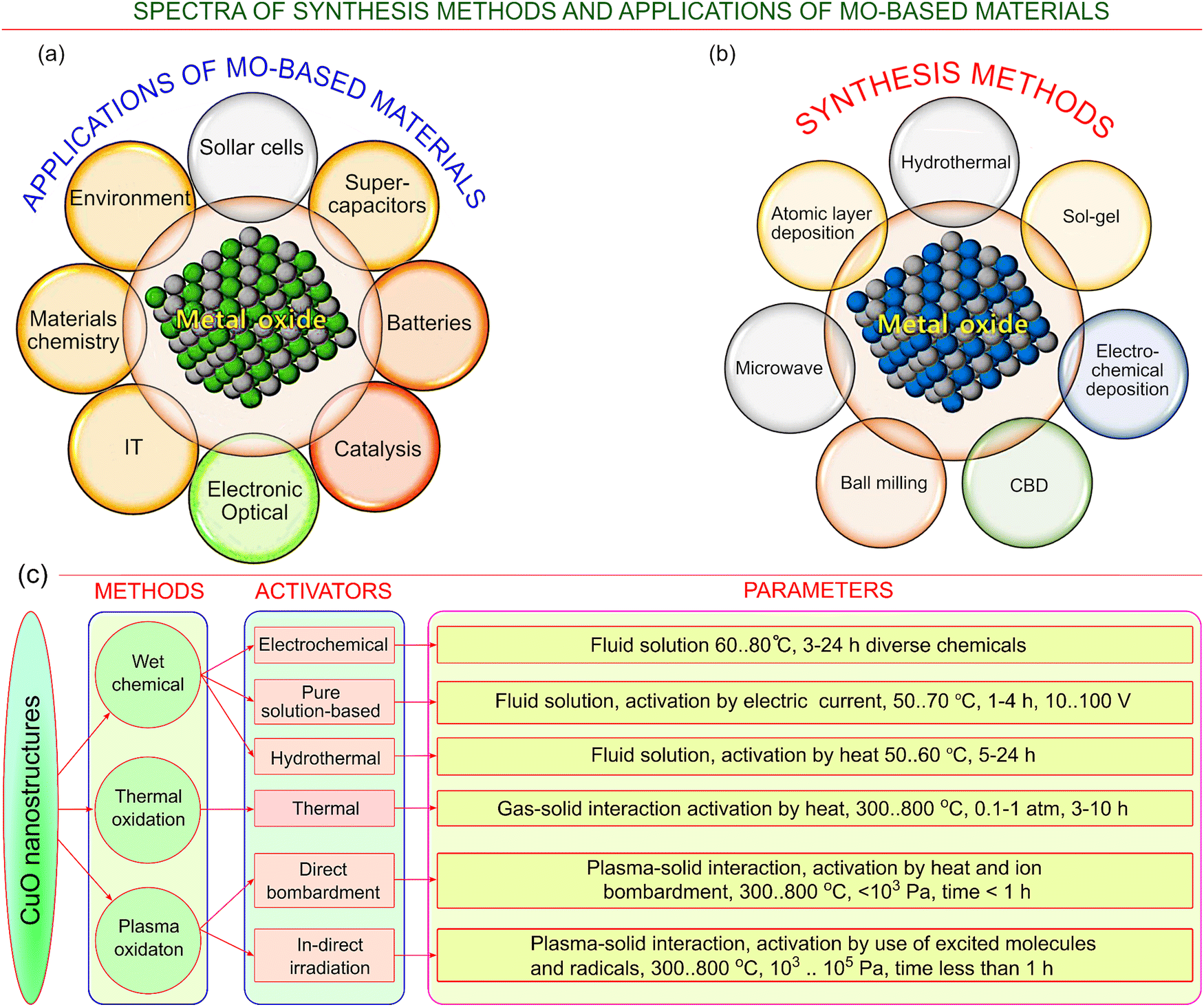 | ||
| Fig. 1 Spectrum of key technologies and applications of metal oxides, and metal oxide (MO)-based materials. (a) The major key technologies and (b) the most important applications of metal-oxide materials. Virtually all important applications could benefit from the implementation of metal oxide-based materials – from optics and IT to energy harvesting and conservation, catalysis and environmental techniques. Adapted from Ansari et al. ref. 65 under conditions of the CC BY license. Copyright 2022. (c) Several key technologies, activators and process parameters specifically for CuO nanomaterials. While the methods can be subdivided into three major groups (wet chemical techniques, thermal and plasma-based methods), the process activators and process parameters demonstrate a flourishing diversity of approaches and conditions, thus offering a great spectrum of possibilities for the future development and sophistication of the MO nanomaterials. | ||
The role of CuO low-dimensional nanomaterials
Similar to many other metal oxide nanostructures, forests of CuO nanowires demonstrate advanced properties that are particularly needed for many applications such as devices for field emission applications,51 batteries,52 supercapacitors,53,54 and others. By contrast, many copper oxide-based nanomaterials and nanostructures feature some intrinsic shortcomings, for example, they have relatively low conductivities, low electrochemical stability and high agglomeration rates. A possible solution for overcoming these shortcomings is to synergistically combine copper oxide-based nanomaterials with other materials such as carbon nanotubes, conducting polymers, and nanomaterials engineered based on graphene hybrids.55,56 This can be achieved via the utilization of various well-established technologies (see Fig. 1b) including low-temperature chemical synthesis,57 high temperature annealing,58 the in situ modification of various copper materials like copper foam,59 anodization in a solution of sodium bicarbonate,60 thermal oxidation of copper nanostructures,61 facile solution-phase treatment techniques,62 oxygen oxidation of foils63 and many other techniques.64Significance of this review
Featuring very high surface-to-volume ratios and high chemical reactivity, low-dimensional copper oxide nanostructures are very promising building blocks for various functional materials, and thus a review of their properties and potential applications will be of great interest to a wide range of researchers, including, but not limited to the following:✓ the use of low-dimensional copper oxide nanostructures may help overcome the challenges and achieve greater performances for devices used in energy harvesting and transformation, sensing, catalysis and biomedical technologies;
✓ copper oxide nanomaterials in general have a very wide spectrum of applications ranging from environmental and biomedical to energy, optics, catalysis and others – moreover, they can be successfully combined with graphene-based materials;
✓ finally, in this review article we discuss the very recent progress – mostly within the past two years – in the design of complex, sophisticated low-dimensional copper oxide-based material systems for various applications, aiming to emphasise some of the most interesting and important, from the authors’ point of view, innovations in the fabrication methods and applications of low-dimensional copper oxide nanostructures.
How are the CuO nanowires formed on the surface?
In many fabrication technologies (Fig. 1c), low-dimensional CuO nanostructures are growing directly on substrates. Apart from the convenience of substrate-utilization processes, this approach is suitable for the production of many important devices, e.g., electrodes for supercapacitors and batteries, catalytic systems, etc., where hierarchical systems consisting of substrates and arrays on nanostructures are required.Fig. 2a shows a schematic of the thermal growth of nanowires on a substrate as well as the key processes that supply material for the growth. Cu2O and CuO oxides grow as follows:66
| Cu2O + O → 2CuO, | (1) |
| CuO + Cu → Cu2O. | (2) |
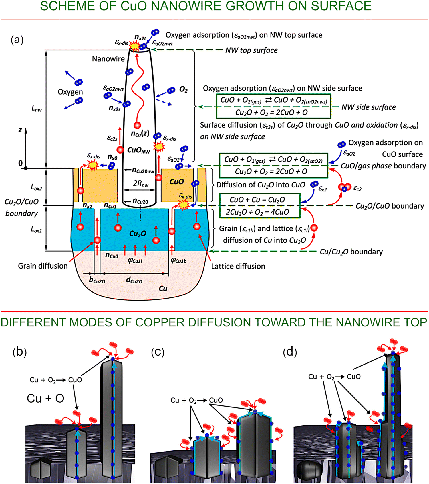 | ||
| Fig. 2 Schemes and processes of CuO nanowire growth on a surface. (a) Schematic of the thermal growth of nanowires on a substrate and the key processes that supply material for the growth. Reproduced with permission from Baranov et al., ref. 66. Copyright 2021, Elsevier. The gradients of copper and oxygen concentrations on the exposed surfaces of CuO oxide, the boundary between Cu2O and CuO oxides, and the boundary between Cu and Cu2O layers are considered as the main driving forces of the process in the formation of CuO nanostructures. Nanowire nuclei are considered as having an anisotropy with respect to the adsorption of oxygen from the gas phase, with the energy of adsorption on the nanowire tips being higher than that on the nanowire side surface; thus, growth on the tips is preferential. Copper atoms are supplied to the surfaces of the nanowires via lattice and grain-boundary diffusion through the Cu2O layer, grain-boundary diffusion through the CuO layer, and surface or grain-boundary diffusion along the length of the CuO nanowire. The density of surface defects of the side surfaces of the nanowires plays an important role in the formation of long nanowires with a high aspect ratio, since for the perfect surface the oxygen adsorption is low, and copper atoms travel from the nanowire root to the tip without being involved in the reaction of oxidation. As a result, the nanowire does not increase in diameter, and the whole copper flux is delivered to the tip. Opposite to that, the defect-containing side surface promotes oxygen adsorption and increases the rate of oxidation on the side surface of the nanowire; thus, short and bulky nanowires are formed. (b–d) Different modes of copper diffusion toward the nanowire top. Reproduced with permission from Baranov et al., ref. 67. Copyright 2022, ACS. | ||
2. Innovations in CuO nanowire fabrication methods
Recently, many advanced techniques for the fabrication of one-dimensional copper oxide nanostructures and arrays have been developed and tested (Fig. 1). Here we will briefly outline the recent innovations in several of the most important technologies for the fabrication of CuO nanostructures, highlighting the examples that exhibit advanced properties for their applications.2.1. Recent innovations in plasma-based and electric field-assisted technologies
Among other technologies, plasma-based approaches for growing various nanostructures are very efficient due to the presence of highly energetic ions that efficiently heat and activate the growing nanostructures, and the presence of electric fields that help to form the targeted structures.70,71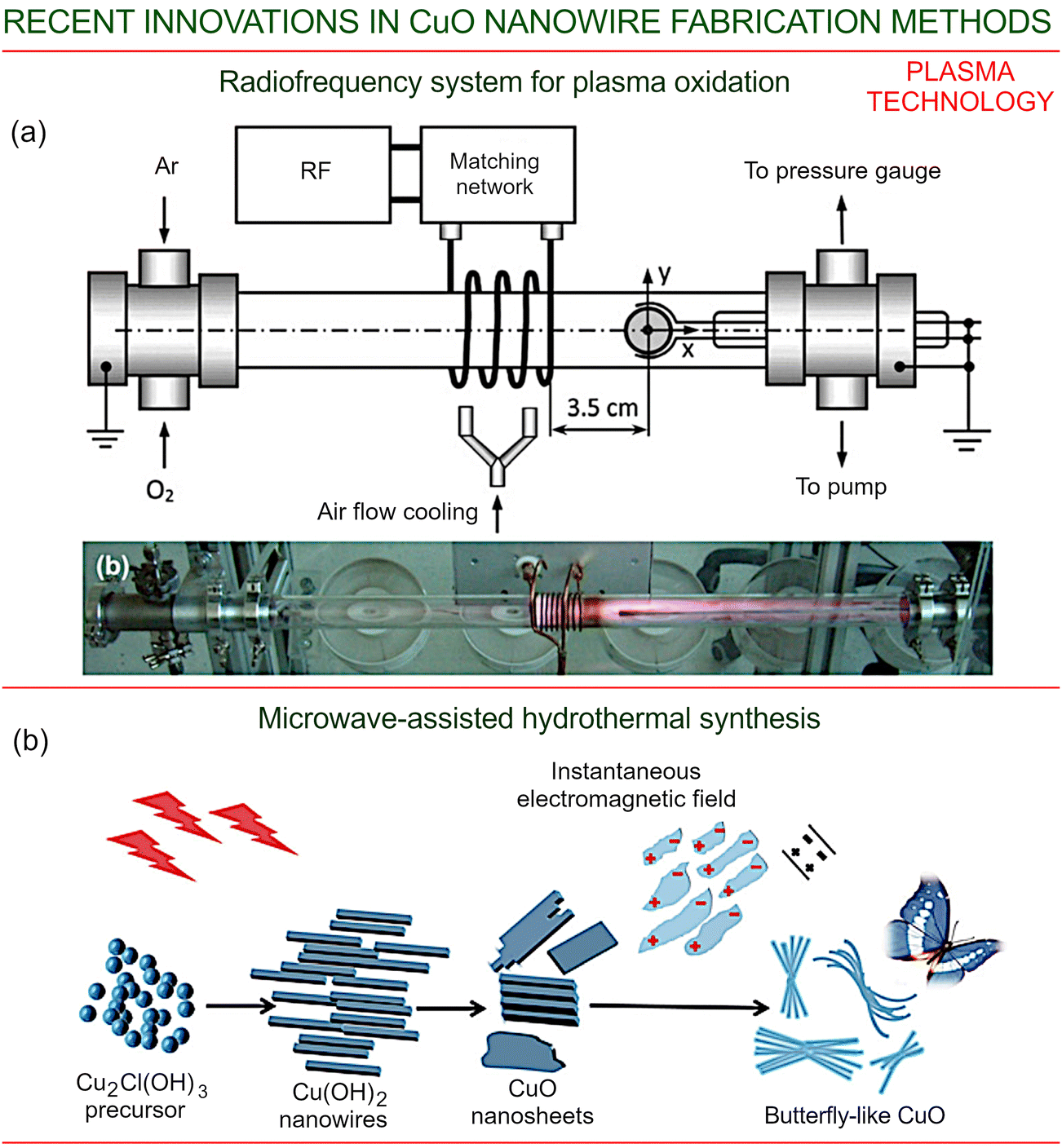 | ||
| Fig. 3 Plasma-based technology for CuO nanowire fabrication. (a) A typical radio-frequency system for copper oxidation and copper oxide nanowire growth in plasma. The inset show an optical photograph of the setup in operation. Reprinted with permission from Filipic et al., ref. 68. Copyright AIP. (b) Synthesis of butterfly-like copper oxide nanostructures using microwave-assisted hydrothermal technology. Reprinted with permission from Li et al., ref. 69. Copyright Springer Nature, 2020. | ||
The system used commercial-grade oxygen and argon for the reactive plasma environment. The gas pressure in the tube was monitored using a system of gauges. During the operation, the tube was cooled using a flow of pressurized atmospheric air. The CuO nanowires were formed using copper disc samples, with dimensions of 10 mm diameter and 1 mm thickness, on which the thin, long (4.5 μm) nanowires were successfully fabricated in this system.68
Fig. 3b illustrates the synthesis of butterfly-like copper oxidation nanostructures using microwave-assisted hydrothermal technology. The energy carried by the microwaves produces heat which facilitates the reaction, enhancing diffusion of the substances and facilitating their attachment and thereby the growth process. The microwaves directly assisted the intermediate formation of Cu(OH)2 nanowires, followed by a dehydration process yielding nanosheets of CuO, to produce an associated orthorhombic to monoclinic structural transformation. Due to their polar properties, the CuO sheets were polarized using the microwaves, and arranged finally into a butterfly-like morphology along the external microwave field. It is observed that the size of the CuO butterfly-shaped structures increases with the duration of the applied radiation, suggesting that microwave fields play an essential role in the formation of these special morphologies.69
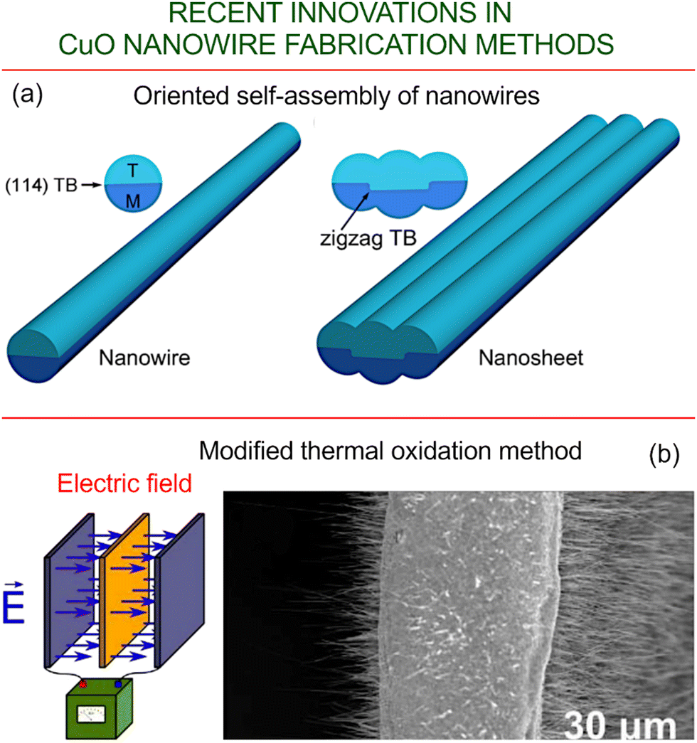 | ||
| Fig. 4 Self-assembly and electric-field assisted growth. (a) Schematic showing the oriented self-assembly of nanowires, featuring the formation of a zigzag twin boundary (TB). Reprinted with permission from Cao et al., ref. 72. Copyright APS. (b) Growth of CuO nanowires, via a modified thermal oxidation method, on both sides of copper foil using an external electric field. Reprinted from Sondors et al. 2020, ref. 73 under terms and conditions of CC BY license. | ||
The growth of CuO nanowires, using an electric-field assisted oxidation method, on both sides of a copper foil has recently been reported by Sondors et al.73 (Fig. 4b). It was found that increased humidity during the early stages of growth produced higher yields of NWs with diameters smaller than 100 nm, and correspondingly large aspect ratios. Moreover, NWs with diameters smaller than 50 nm possess unusually large Young's moduli in the range of 200–500 GPa. Regarding their electrical properties, the NWs display relatively large electrical resistivities, comparable to those of CuO NWs, and were higher than those obtained when the electric field was applied in wet air. These findings are quite interesting since a combination of low conductivity and high stiffness is excellent for the design of nanoelectromechanical switching devices intended for operation under extreme environmental conditions, such as under high voltages or in harsh environments.
An example of the plasma-based deposition system is shown in the upper panel of Fig. 5.74 This system is suitable for the production of nanostructures with different morphologies (NWs, nanobelts, etc.) from various metal oxides including zinc, iron, and copper. Examples of such CuO nanostructures are presented in Fig. 5. Copper oxide NWs can be grown on thin copper foils, yielding structures of different diameters and lengths, depending on the temperature. For example, at 300 °C the mean diameter and length values are about 70 nm and 0.8 μm, respectively, while at 400 °C they increase to 600 nm and 1.4 μm, respectively. The presence of single-crystalline structures associated to form CuO NWs can be revealed using TEM analysis, examples of which are shown in Fig. 5d and e for the case of treatment at 300 °C and of 30 min duration.
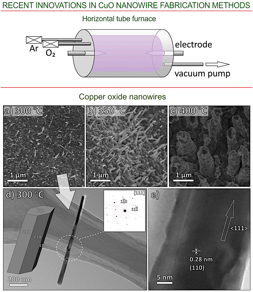 | ||
| Fig. 5 Plasma-based synthesis of CuO nanowires. Upper panel: schematic of the plasma-assisted furnace deposition chamber contained within a vacuum-sealed glass tube, showing the two pointed-end electrodes that are used to ignite the plasma. Bottom panel: (a–c) SEM images of the copper oxide nanostructures synthesized at different growth temperatures for growth time of 30 min; (d) TEM image of a single copper oxide nanostructure grown at 300 °C viewed along the [111] zone axis and a nanowire model in the same orientation (inset shows the selected-area electron diffraction pattern); and (e) high-resolution TEM image of the copper oxide nanostructure with the marked interplanar spacing. Reprinted from Guo et al., ref. 74 under terms and conditions of CC BY license. | ||
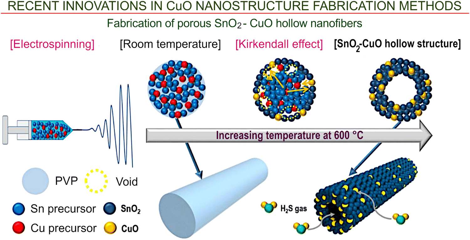 | ||
| Fig. 6 Electrospinning combined with thermal processing. The fabrication of porous SnO2–CuO hollow nanofibers for gas sensors via electrospinning combined with thermal processing. Reprinted from Park et al. 2020, ref. 75 under terms and conditions of CC BY license. | ||
The listed examples prove that the synthesis method of the CuO nanostructures greatly affects their performance. Up to now, a number of chemical methods have been developed to synthesize CuO nanostructures. CuO nanowires and nanosheets have been grown directly on copper sheets in alkaline solution via single-step voltammetry in the experiments of Singh et al.76 Kulkarni et al.77 reported the synthesis of copper oxide nanowires via a facile solution-phase method, and the formation of CuO nanowires obtained via anodization in sodium bicarbonate solution was studied by Gizinski et al.78 Other chemical79,80 or plasma-enhanced81 methods have also been developed and have the advantages of being controlled easily through involving the presence of reagents, or electric and magnetic fields.82,83
2.2. Recent innovations in thermal and wet-chemical technologies
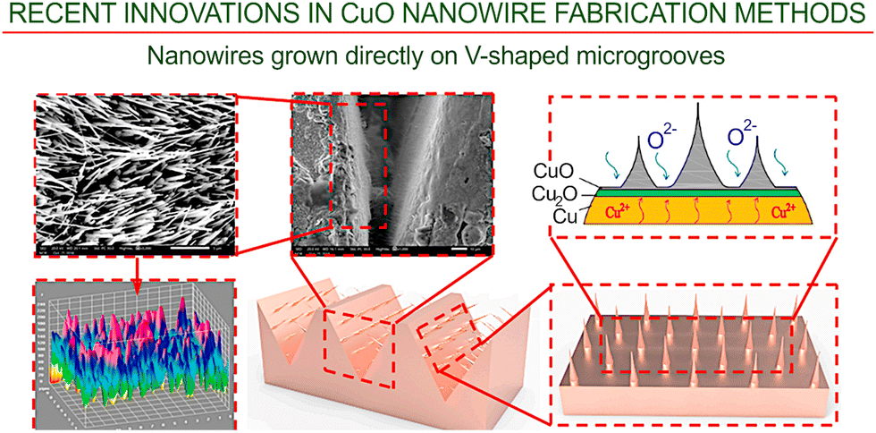 | ||
| Fig. 7 Nanowires grown directly on V-shaped microgrooves. After thermal oxidation, the nanowires were grown directly on V-shaped microgrooves. Importantly, it was found that both microvoids and microcavities appear to play an essential role in the process. Reprinted with permission from Deng et al., ref. 84. Copyright 2021, Elsevier. | ||
The thermal oxidation results discussed so far are indissolubly linked to a diffusion process of CuO along grain boundaries, in which a Cu2O layer is formed that acts as the precursor for the incipient NWs. Generally, the length of the nanowires increases with the annealing time. For example, the average length of 5.1 μm was obtained in the case of 2 h of treatment, which increased to 10.2 μm after 8 h of treatment, confirming the effect of the annealing time on the length. By contrast, the NW diameter turns out to be almost independent of the treatment time. This is attributed to the fact that the NW diameter is highly dependent on the grain size, which determines the cross-section geometry of the wires, but which is not sensitive to thermal annealing.
The results obtained by Jafari et al.86 support the above-mentioned conclusions, although at higher temperatures, in the range of 500–700 °C. At 700 °C, nanowires form denser arrays reaching 1–3 μm in length, thus suggesting that compressive stress is important for determining both the nanowire diameter and density. They show remarkable photocatalytic properties and electrical conductivity, which could be associated with different electron scattering mechanisms. This general picture was also confirmed by Mahmoodi et al.,87 who performed experiments at the lower temperature of 400 °C, in which the NW length increased from about 1 μm after 5 h to 2–3 μm after 5–7 h, and to 2.5–3.5 μm after 7–9 h of annealing time. As expected, the NW diameter was insensitive to the treatment time, falling within the range of 50–70 nm.
Experiments reported by Feng et al.88 were performed at three temperatures (400, 450, and 500 °C) and at treatment durations ranging from 4 to 12 hours. They confirmed that both the diameter and the length of the nanowires increased with temperature and the growth time. Differences in aspect ratio trends were observed when varying either the temperature at a fixed time of growth or the growth time at a fixed temperature. Interestingly, a maximum diameter was found at around 8 h for each temperature considered.
Interesting technology has been recently reported by Sun et al.85 A Cu wafer was used as the source of copper for the initial synthesis of Cu2S nanoparticles. During the oxygen evolution reaction, sub-micrometer Cu2S particles transformed into nanowire-like CuO nanostructures (Fig. 8).
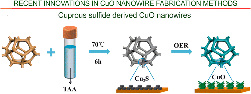 | ||
| Fig. 8 Cuprous sulfide derived CuO nanowires. Synthesis of Cu2S/CF and the related phase change during operation of the oxygen evolution reaction (OER). Reprinted with permission from Sun et al., ref. 85. Copyright 2021, Elsevier. | ||
Thermal oxidation was used recently to fabricate detectors with a high level of sensitivity, as well as a fast and stable photoresponse to visible light, using well aligned copper oxide nanowires.96 The absorption of visible light was increased substantially by exploiting the interference effects that occur in nanowire arrays of certain geometry. The desired combination of geometry and alignment was realized through the use of an SiO2 template that was fabricated using repeated cycles of wet-chemical oxidation and etching, as they enable the generation of 3D arrays of regularly spaced, well-aligned nanoscale structures on larger surfaces with high (1 nm) resolution (Fig. 9b). The glancing angle deposition (GLAD) technique was then used to grow copper nanowires on the surface of the thus-fabricated SiO2 template, with high-temperature oxidation at 700 °C for 3 h in air then used to covert Cu into CuO. Next, gold electrodes were deposited by first coating the surface of the CuO nanowires with a photoresist via spin coating, growing a layer of Au using PVD, and then removing the photoresist. SEM images of the obtained structure and schematics of the device are shown in Fig. 9.
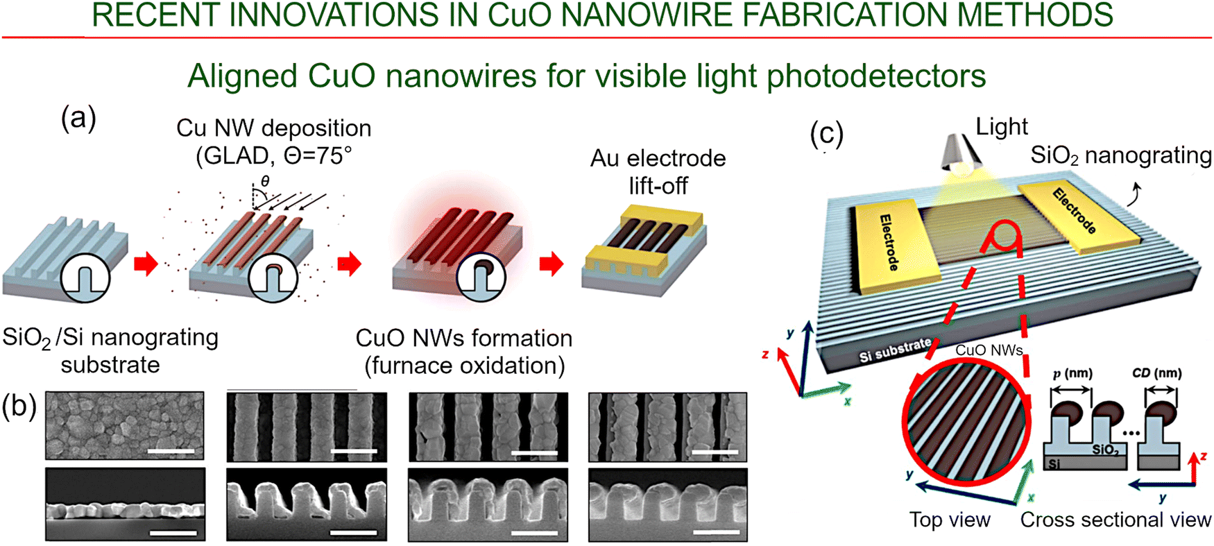 | ||
| Fig. 9 Aligned CuO nanowires for visible-light photodetectors via thermal oxidation. (a) Method for the growth of well-aligned CuO nanowires using a combination of substrate nanograting, GLAD and furnace oxidation, with the subsequent deposition of Au electrodes using a combination of photoresist lithography and physical vapor deposition. (b) SEM images of the copper oxide film and nanowires with critical dimensions. Top views are shown in the upper panels, and cross-section views are shown in the bottom panels. The length scale is 500 nm. (c) Structure of the photodetector illustrating the placement of copper oxide nanowires on the surface of the patterned SiO2. Reprinted under terms and conditions of CC BY license from Jo et al., ref. 96. Copyright 2022, the Authors. | ||
Fig. 10a illustrates an interesting example of the application of the wet-chemical process to fabricate ultrathin CuO nanowires using self-assembled Cu(OH)2 as the starting material.97 Cu(OH)2 NW structures are fabricated from an inorganic colloidal suspension of Cu(OH)2, where the selective adhesion of organic solvent molecules changes the surface energy of the inorganic crystal, which in turn drives the aggregation of crystallites and, from a practical standpoint, enables the fabrication of aggregates with the desired size and shape. In this particular study, such directed crystallite growth was used to produce Cu(OH)2 NWs with an average aspect ratio of >112. Subsequent annealing of the thus-produced Cu(OH)2 NWs resulted in the formation of CuO nanowires, where the length of the nanowire remained similar (∼7 μm), and the average diameter of the CuO nanowires increased six-fold, to ∼27 nm. This simple approach provides a potentially useful avenue for the fabrication of electronically-active nanostructures with the desired size and shape configurations.
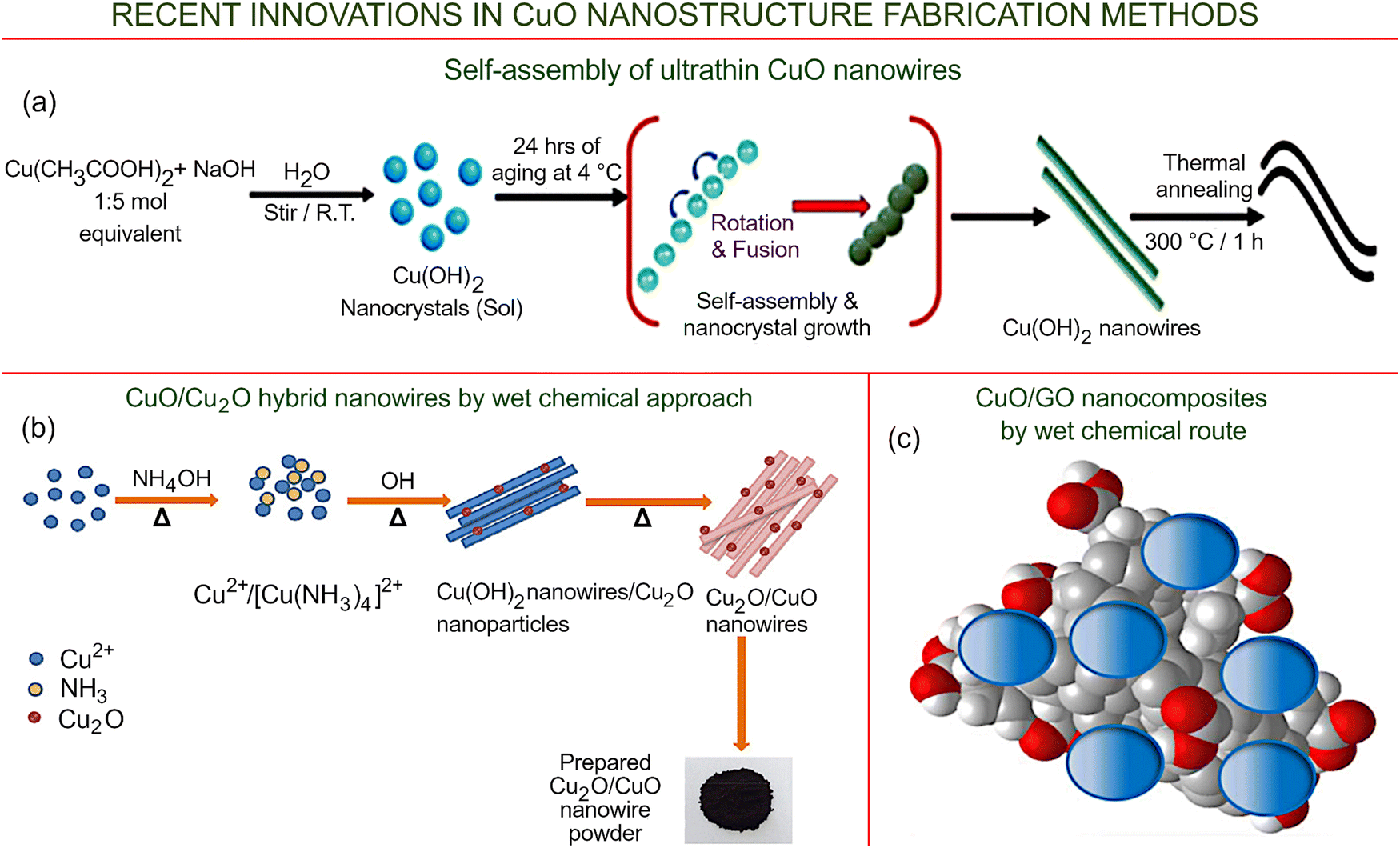 | ||
| Fig. 10 Wet-chemical and hydrothermal technologies. (a) Illustration of the chemical reaction pathway and the subsequent self-directed growth of Cu(OH)2 colloidal particles, followed by their thermal conversion to copper oxide nanowires. Reprinted under terms and conditions of CC BY license from Pathiraja et al., ref. 97. Copyright 2020, the Authors. (b) Likely pathway for the formation of hybrid CuO/Cu2O nanowires. Reprinted with permission from Sahu et al., ref. 98. Copyright 2020, Elsevier. (c) CuO/GO nanocomposites produced via wet-chemical synthesis. Reprinted under terms and conditions of CC BY license from Biswas et al., ref. 99. Copyright 2021, the Authors. | ||
Another interesting material that is currently being investigated is the so-called ‘hybrid’ CuO/Cu2O nanowires, for which the mechanism of formation is illustrated in Fig. 10b.98 The CuO/Cu2O nanowires were synthesized directly from copper acetate, which is both abundant and affordable, using wet chemistry. This very simple process consisted of mixing the copper acetate solution in double-distilled water with ammonia solution, followed by thorough stirring and the addition of sodium hydroxide. The synthesis was conducted at 90° for two hours, with stirring. After keeping the solution overnight at room temperature, precipitates that had formed were centrifuged, washed with distilled water and ethanol, and dried. Despite the remarkable simplicity and low price of this technology, the resultant material has demonstrated an extremely high efficiency when used as a catalytic platform for the effective conversion of 4-nitrophenol to 4-aminophenol, the former being a phenolic compound that is used widely in the fabrication of pesticides, drugs, and synthetic dyes, and which is known to be harmful. The conversion of 4-nitrophenol to 4-aminophenol is a reaction that is also commonly used in the synthesis of analgesics and antipyretic pharmaceuticals, including paracetamol. The efficiency with which the CuO/Cu2O nanowires catalyzed the conversion reaction emphasizes the potential of wet-chemical processes for the nano-synthesis of advanced nanomaterials.
Wet chemical routes also enable the fabrication of very important and promising copper oxide–graphene oxide (CuO/GO) nanocomposite materials. In a recently reported study, a bottom-up approach was used for the synthesis of copper oxide nanoparticles directly on the surface of graphene oxide flakes, the latter being a hydrophilic material. The resulting composites of copper oxide and graphene oxide were obtained by combining two specific precursors, copper nitrate and citric acid, intermittently mixed with graphene oxide solutions.99 Importantly, the formation of the C![[double bond, length as m-dash]](https://www.rsc.org/images/entities/char_e001.gif) C, C–O, and Cu–C functional groups was confirmed using FTIR analysis. Morphologically, the composite material consists of CuO nanoparticles deposited on planar hydrophilic graphene oxide sheets (Fig. 10c). These results suggest the possibility of synthesizing nanomaterial-based devices with a high degree of sensitivity that can be used simultaneously for diagnostics and therapy, leading to the development of new solutions in healthcare.
C, C–O, and Cu–C functional groups was confirmed using FTIR analysis. Morphologically, the composite material consists of CuO nanoparticles deposited on planar hydrophilic graphene oxide sheets (Fig. 10c). These results suggest the possibility of synthesizing nanomaterial-based devices with a high degree of sensitivity that can be used simultaneously for diagnostics and therapy, leading to the development of new solutions in healthcare.
The top panel of Fig. 11 illustrates one of the ways by which petal-shaped nanoparticles of copper oxide can be grown using hydrothermal technology. The thus-obtained petal-shaped monoclinic nanocrystals display a high size uniformity, a considerable surface area and desirable morphological characteristics. Importantly, hydrothermal technology appears to be well suited for the synthesis of petal-like copper oxide nanostructures due to its relative simplicity and affordability, the purity of the resulting products, the high reproducibility of the results, the lower defect levels in comparison with other methods that require high temperatures, and, finally, its remarkable ability to be scaled up for the fabrication of monodisperse copper oxide nanostructures in larger quantities.100 To fabricate the CuO nanopetals, powdered copper nitrate is first combined with water to produce a uniform dispersion, which is then introduced into an aqueous solution of hexamethylenetetramine at ambient temperature with thorough stirring. Next, the thus-obtained solution is heated to 110 °C for about 3 h under elevated pressure. Finally, it is cooled to ambient temperature, followed by centrifugation and washing. The black solid material produced as a result of this process is then subjected to drying under a nitrogen flow in a vacuum oven. Thus, this process is also very simple, cheap, and does not demand the use of complex and/or expensive equipment. Nevertheless, the produced CuO nano-petals demonstrate an advanced (above 99% in 90 min) catalytic activity for the degradation of methylene blue in the presence of hydrogen peroxide.
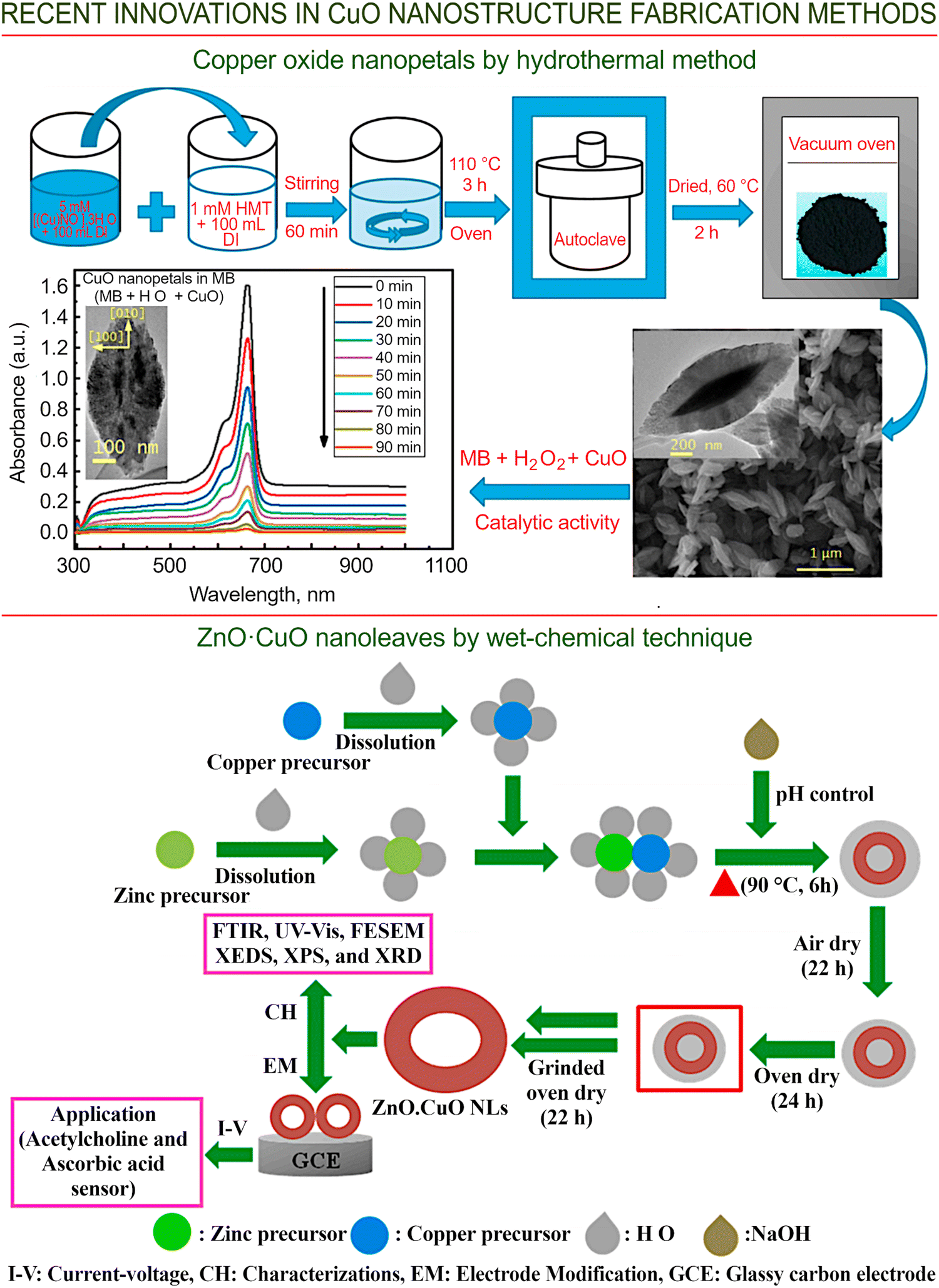 | ||
| Fig. 11 Wet-chemical and hydrothermal technologies. (Top panel) Petal-shaped CuO nanostructures grown using hydrothermal technology, and their application in catalysis (MB denotes methylene blue). Reprinted under terms and conditions of CC BY license from Khan et al., ref. 100. Copyright 2020, the Authors. (Bottom panel) Synthesis of sensors for the detection of acetylcholine and ascorbic acid using zinc oxide/copper oxide leaf-shaped nanostructures fabricated using wet chemistry. Reprinted with permission from Hussain et al., ref. 101. Copyright 2020, Elsevier. | ||
Zinc oxide-doped copper oxide (ZnO·CuO) nanoleaves for the non-enzymatic detection of acetylcholine and ascorbic acid were synthesized using a facile wet-chemical technology (Fig. 11, lower panel). Cheap reagents (i.e., zinc chloride, copper sulfate and NaOH) were used. Zinc chloride and copper sulfate were dissolved in water, stirred, and the pH of the solutions was adjusted using NaOH. Next, the solutions were stirred for 6 hours at 90 °C. After evaporation and drying, the material was ground to a powder.101 The prototype sensor fabricated using this material is capable of detecting acetylcholine and ascorbic acid in samples of human, mouse, and rabbit serum, as well as in orange juice and urine.
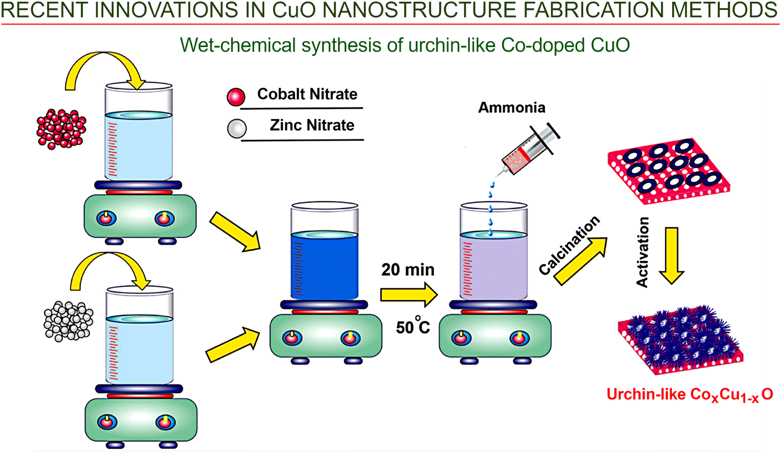
Wet-chemical technology was also used to produce urchin-like cobalt-doped copper oxide nanostructures for antimicrobial applications and the removal of organic pollutants from water.102 The Co-doped CuO sample was prepared using relatively cheap reagents such as cobalt nitrate hexahydrate, liquid ammonia and ethanol via wet co-precipitation technology. Cobalt and copper salt solutions were mixed and then agitated for 20 min at 50 °C, where stirring if the mixture was continued until precipitation of the residue was achieved, before drying (Fig. 12). Finally, the produced CoxCu1−xO was chemically activated using KOH. Despite its simplicity and affordability, this approach of combined Co doping and activation has the potential to bring about a notable increase in the performance of copper oxide as a catalytic platform in under visible light.
 | ||
| Fig. 12 Wet-chemical and hydrothermal technologies. Fabrication of Cox–Cu1−xO nanostructures with an urchin-like morphology. The Co-doped CuO nanostructures were prepared using cheap reagents such as cobalt nitrate hexahydrate, liquid ammonia and ethanol via wet co-precipitation technology. Reprinted with permission from Alburaih et al., ref. 102. Copyright 2022, Elsevier. | ||
The preparation of binary metal doped CuO nanocatalysts using liquid reagents is one more example of the wet chemistry application to produce advanced nanomaterials. Doping CuO nanoparticles with cerium and zinc enabled the fabrication of the CeZn·CuO photocatalyst with superior activity.105 In this process, liquid ammonia was used, simultaneously, as the precipitating agent and pH regulator. This simple co-precipitation technology involving the mixing and stirring of respective hydrated nitrate solutions of cerium, zinc and copper, followed by the addition of ammonia solution as the precipitation agent, resulted in the formation of a nanomaterial, which was then washed and dried, before being ground and annealed at 750 °C (Fig. 13). CeZn·CuO was able to degrade 81.64% MB dye in 100 min.
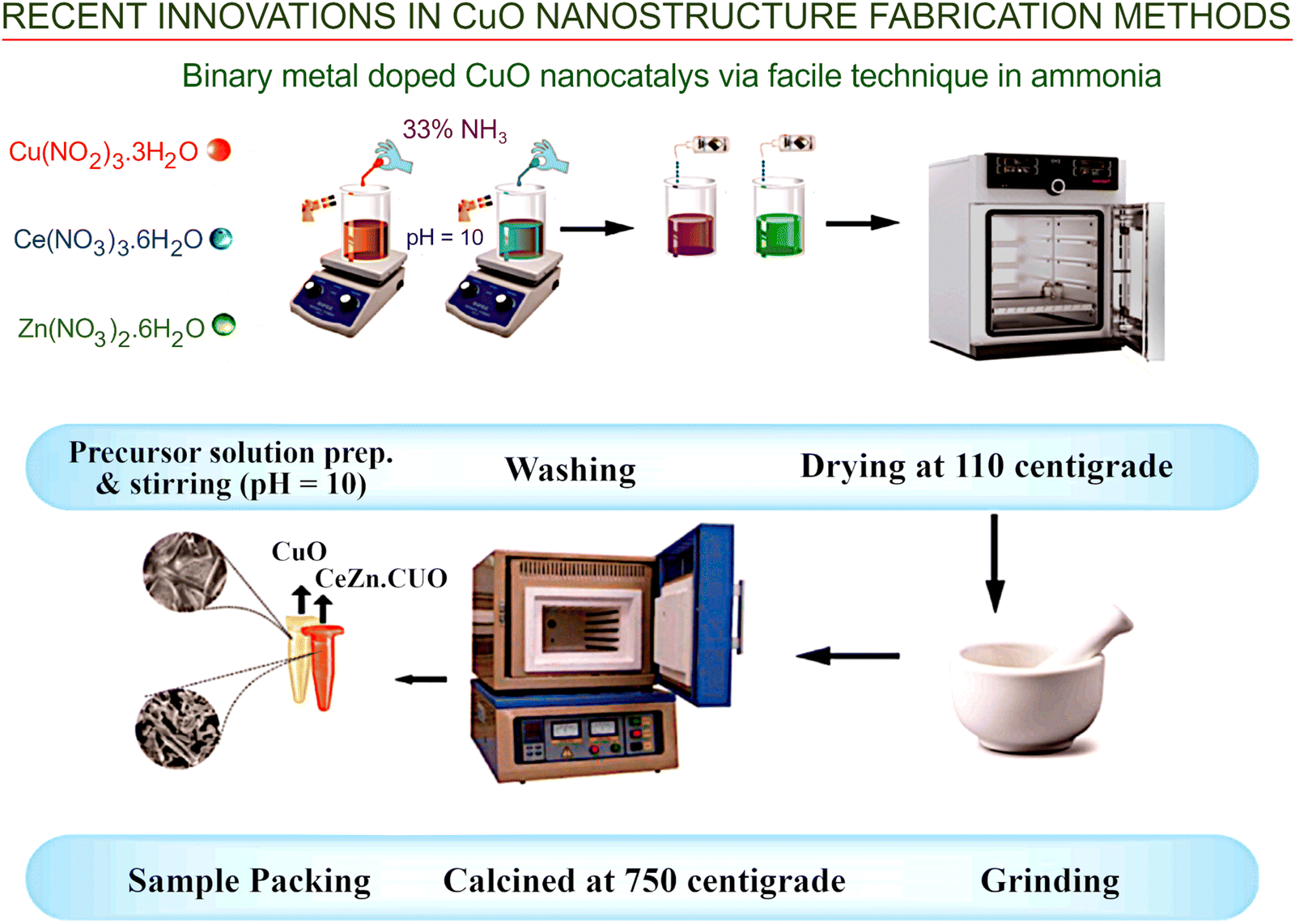 | ||
| Fig. 13 Wet-chemical and hydrothermal technologies. Synthesis and assembly of CuO nanocatalysts doped with a binary metal. Doping CuO nanoparticles with cerium and zinc enabled the fabrication of CeZn·CuO photocatalyst with superior activity. Liquid ammonia was used as a precipitating agent and pH regulator, simultaneously. Reprinted with permission from Rehman et al., ref. 105. Copyright 2021, Elsevier. | ||
2.3. Effect of process parameters: recent insights
Zúñiga et al. synthesized NWs of 0.3 mm in diameter at 400 °C and 500 °C in air for about 2 h.106 At the two temperatures, both the diameter and length of the NWs were found to increase with time, and the NWs were found to be composed of bi-crystals. Mohamed et al. investigated NW formation from Cu2O/CuO composites via the thermal oxidation of 0.51 mm thick copper foil at 550 °C, 600 °C, and 650 °C, employing as the input an Ar (100 sccm) and O2 (50 sccm) gas mixture for about 4 h.107
The NW diameter and length results for the three temperatures considered (550, 600 and 650 °C) were as follows: 95–250 nm, 9 μm; 105–295 nm, 12 μm; and 100–295 nm, 30 μm, respectively. It was found that at 650 °C, some of the NWs break down when their length exceeds a certain value. This was thought to be due to a mismatch between the Cu2O and Cu lattices, producing a larger amount of stress, indicating that the release of such a significant stress is the actual driving force for the NW growth. A model was proposed by Zhu et al.108 to explain how NW bi-crystals can be formed, leaving open the question about mono-crystalline NWs, as mentioned by Zhang et al.109 Besides, two main mechanisms for copper diffusion to the NW top have drawn most attention in the literature:110 one is the diffusion via a twin boundary, and the second is just the surface diffusion of Cu ions on the NW surface itself. Moreover, important results were recently reported by Hu et al. who grew CuO nanoneedle arrays on top of commercial ceramic tubes using magnetron sputtering,111,112 followed by both wet chemical etching and annealing.113Fig. 14 (upper panel) illustrates the scheme of the process, and Fig. 14 (lower panel) shows the SEM images of the obtained nanostructures. This technology opens the way to the fabrication of cheap tube-like gas sensors.
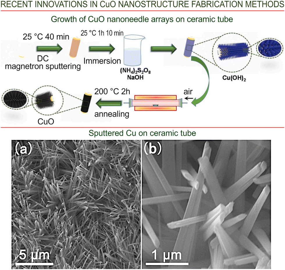 | ||
| Fig. 14 (Upper panel) Schematic of CuO nanoneedle arrays grown on a commercial ceramic tube. (Lower panel) SEM images at low (a) and high magnification (b) of sputtered Cu on the ceramic tube after wet etching. The nanoarrays are able to keep their morphology after a calcination process at 200 °C. Reprinted with permission from Hu et al., ref. 113. Copyright 2021, Elsevier. | ||
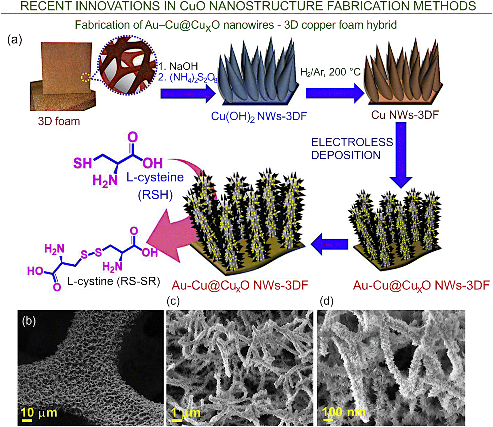 | ||
| Fig. 15 Hybrid system based on gold nanoparticles and a CuxO nanowire–3D copper foam. (a) Schematic of the fabrication of the Au–Cu@CuxO nanowire–3D copper foam hybrid. (b–d) SEM images of the synthesized Au–Cu@CuxO nanowire–3D foam hybrid structure. Reprinted with permission from Le et al., ref. 128. Copyright 2019, Elsevier. | ||
2.4. Recent insights into the driving forces for one-dimensional growth
The question of the driving force for the 1D formation of long nanostructures is still under debate.129 Among the possible NW growth mechanisms, vapour–solid (VS) and vapour–liquid–solid (VLS) approaches are not appropriate for temperatures in the range of 300–800 °C, which are well below the melting point of Cu or its oxide compounds. Recent experiments have suggested that CuO NWs can grow on their tops,130,131 suggesting that Cu should be supplied to the tops of nanowires, thus enabling their reaction with oxygen. As we already mentioned above, the possibilities of this can occur via Cu diffusion either along the grain boundaries or on the NW surface.131 However, both explanations have some drawbacks. For instance, in the case of surface diffusion, one would expect thicker NWs at the bottom, while most of the available results point to a uniform NW width distribution. If the diffusion along the grain boundary is assumed, one cannot explain Cu diffusion for cases in which grain boundaries are not present, which have been indeed observed in experiments. Interesting results were obtained by Chen et al. with respect to the effect of the annealing time: a large number of long thin nanowires were grown at 500 °C and 8 hours of exposure, and only CuO crystallites were developed at the same temperature but for 24 hours of annealing.132 The results are a possible manifestation of the fact that the reaction between oxygen and copper takes place at the side of the NW surface or on its defects, without the need to invoke any of the above-mentioned mechanisms or even in synergy with them.A complex study revealing the role of gold decoration on the growth of copper oxide nanowires was carried out by Mishra et al.138 The authors used the following technology sequence (Fig. 16): first, an initial array of CuO nanowires was grown until saturation using a microwave plasma at atmospheric pressure; then, the array was covered with separated gold nanoparticles; next, a second plasma oxidation treatment was carried out. It was predicted and verified that the growth of the nanowires re-started during the second oxidation. A combination of growth in plasma, where the nanowires grow quickly to the saturated length, and then the deposition of metals followed by a second exposure to plasma results in changing the morphology of the nanowires, thus providing an effective tool for control over their physical and chemical properties.
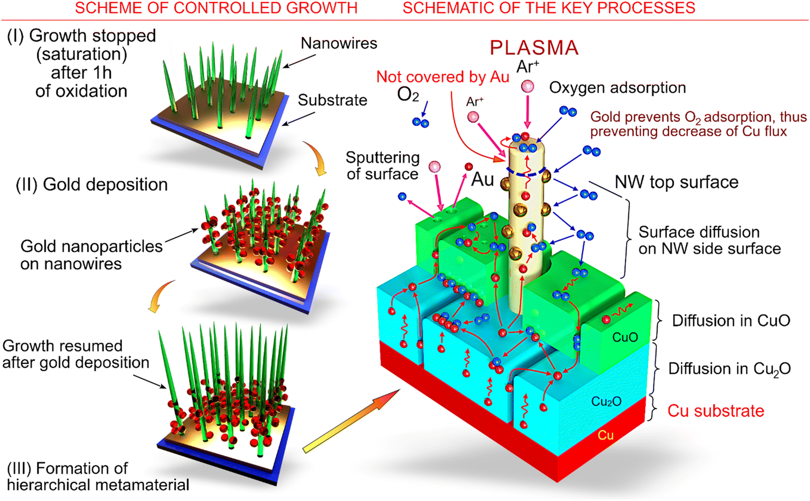 | ||
| Fig. 16 (Left panel) Stages of the designed deposition-controlled growth of nanowires: (I) oxidation of copper; (II) deposition of Au nanoparticles; and (III) second oxidation. (Right panel) Formation of a hierarchical metamaterial from nanowires decorated with Au metal nanoparticles. | ||
The saturation was explained using a model that took into account the mechanism of ion bombardment under the action of low-pressure plasma.139 In contrast, the atmospheric oxygen plasma applied in the present experiment, contains a large number of radicals, electrons, dissociated oxygen atoms and oxygen molecules; the absence of ions means that this plasma can be considered as ‘mild’ with respect to the damage caused by an ion-containing low-pressure plasma. The presence of the oxygen radicals results in much a more intensive oxidation of the copper sample surface, as was demonstrated in the experiments; the excited molecules cause oxidation of the copper samples at relatively low temperatures. The oxide layer usually consists of two sub-layers, namely copper(II) oxide (or cupric oxide (CuO)), and copper(I) oxide (or cuprous oxide (Cu2O)). Both oxides are formed because of the diffusion of the species, which can be via lattice, boundary, or surface diffusion. In this case, the copper atoms moving from the copper layer are involved in the oxidation process on the side surface of the growing nanowire. The prolonged growth results in a decrease of the copper flow delivered from the NW base to the NW top, and the longer the NW, the lower is the supply of the copper atoms. At a certain stage the growth is terminated because all the copper is oxidized on the path to the NW top (Fig. 16). However, the intermediate deposition of noble metal enables the NW growth to be prolonged through the following mechanism. Noble metals do not interact with oxygen, thus the surface of the noble metal deposited on the side surface of the nanowires is relatively free of oxygen. More copper atoms can reach the top because the noble metal deposition decreases the density of adsorbed oxygen on the side surface of the NWs and the generation of copper oxide. As a result, copper is delivered further to the NW tip, where it is involved in a reaction with the oxygen adsorbed on the NW tip, and the NW continues to grow to a longer length.
✓ Thus, many different techniques and methods have been developed and enhanced recently to produce various types of CuO nanostructures with low dimensionality. Below we will outline some recent innovations in the application of such structures, focusing mainly on energy, photocatalysis and sensing as the most important fields.
3. Innovations in the application of CuO nanowire-based metamaterials
First, we stress that the application of CuO nanostructures for energy, photocatalysis and sensing usually requires sophisticated functionalization to impart additional properties and ensure the high performance of CuO-based devises. The functionalization of CuO nanostructures with noble metal nanoparticles is one of the more promising techniques for enhancing the properties of CuO-based devices. Gold nanoparticles, among others, play a particularly significant role because of their catalytic activity and broad range of potential applications.140 Au-based materials have many potential applications in catalysis, in oil hydro refining, as drug carriers and electrode materials, in solar cells, organic synthesis, and in water and air purification.141 Metal oxide–Au and graphene–Au sensors,142 photocatalytic materials,143 photoelectrodes,144 label-free biosensors,145 materials for photoelectrochemical applications,146 integrated electrochemical sensors,147 and free-standing biosensors for the non-enzymatic detection of H2O2148 are recently reported examples of metal-oxide and graphene-based metal-functionalized nanomaterials. Copper oxide nanostructure are no exception, and can often undergo similar treatment with successful practical implementations.3.1. Innovations in CuO nanowire-based metamaterials for sensing
In the study conducted by Yang et al.,149 sensitive CuO/Ag substrates were synthesized using thermal oxidation and magnetron-assisted sputtering. Their surface-enhanced Raman scattering (SERS)150 activity was enhanced by exploiting the rich CuO NWs built on the surface of the nanostructures. Since the Ag work function is 4.1 eV and that of CuO is 5.3 eV, electrons will move to CuO when CuO NWs are covered by an Ag film, thus bringing the Fermi level to equilibrium. Therefore, one expects that combining “positively charged” Ag with “negatively charged” CuO will create a stronger electromagnetic field in response to the specific laser irradiation. Since the CuO/Ag NW array is rather sparse, the molecules prompted for the surface analysis will diffuse across the system, thus enhancing the Raman signal. It should be noted that in the future, copper oxide nanostructures may be used even more efficiently for signal amplification in the SERS-based detection of biomolecules with Au and other noble metals films through hot-spot field enhancement.151CuO nanoneedles on a commercial ceramic tube113 were tested as an excellent H2S gas sensor. The authors concluded that further improvement could be made by designing heterojunctions supplemented with suitable modification of CuO the NW arrays (Fig. 17). Hierarchical nanostructures built upon Au nanoparticles and CuO NWs have been implemented by Zhao et al.152 for use as portable enzymeless glucose detectors. Le et al.128 successfully developed such hybrid systems as biosensors, aimed at L-cysteine detection, displaying properties of a wide detection range, lasting stability, and excellent selectivity. The emerging synergistic effects boosted the sensing performance by improving the exposure of the relevant electroactive sites, accelerating the rate of charge transfer, and increasing the specific surface area. The latter was the result of a prominent 3D hierarchical nanoarchitecture, characterized by impressive mechanical properties that enhance the electrolyte penetration, the diffusion of ions, mass transfer, and the ability to increase charge transfer.
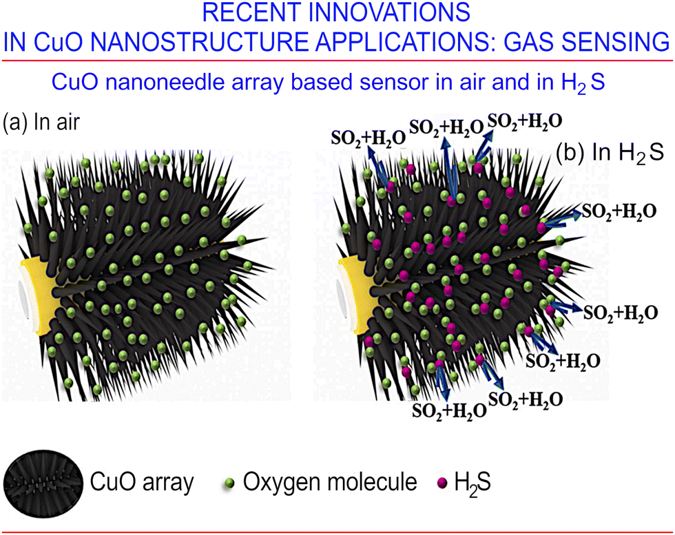 | ||
| Fig. 17 CuO nanoneedle array-based H2S gas sensor. (a) Sensor based on CuO nanoneedle arrays in air, and (b) in H2S. In addition, the system performance can be further improved by building a heterojunction, followed by suitable noble metal modification of the CuO nanowire arrays. Reprinted with permission from Hu et al., ref. 113. Copyright 2021, Elsevier. | ||
Aluminum-doped CuO nanoleaves can also be used for the development of carbon monoxide sensors (Fig. 18)153 A co-precipitation technology was employed to produce doped copper oxide nanostructures, which were then employed as basic building blocks for the fabrication of cheap sensors for the detection of carbon monoxide with high sensitivity at low working temperatures. The sensitivity of the CO sensors to various gas concentrations was investigated over a very wide range of 35 to 12![[thin space (1/6-em)]](https://www.rsc.org/images/entities/char_2009.gif) 500 ppm, and at temperatures in the range of 70–230 °C. While pure CuO nanostructures showed a response of about 50% at 120 °C, the response of aluminum-doped nanoleaf-shaped coper oxide structures was substantially stronger, at nearly 70% at 150 °C.
500 ppm, and at temperatures in the range of 70–230 °C. While pure CuO nanostructures showed a response of about 50% at 120 °C, the response of aluminum-doped nanoleaf-shaped coper oxide structures was substantially stronger, at nearly 70% at 150 °C.
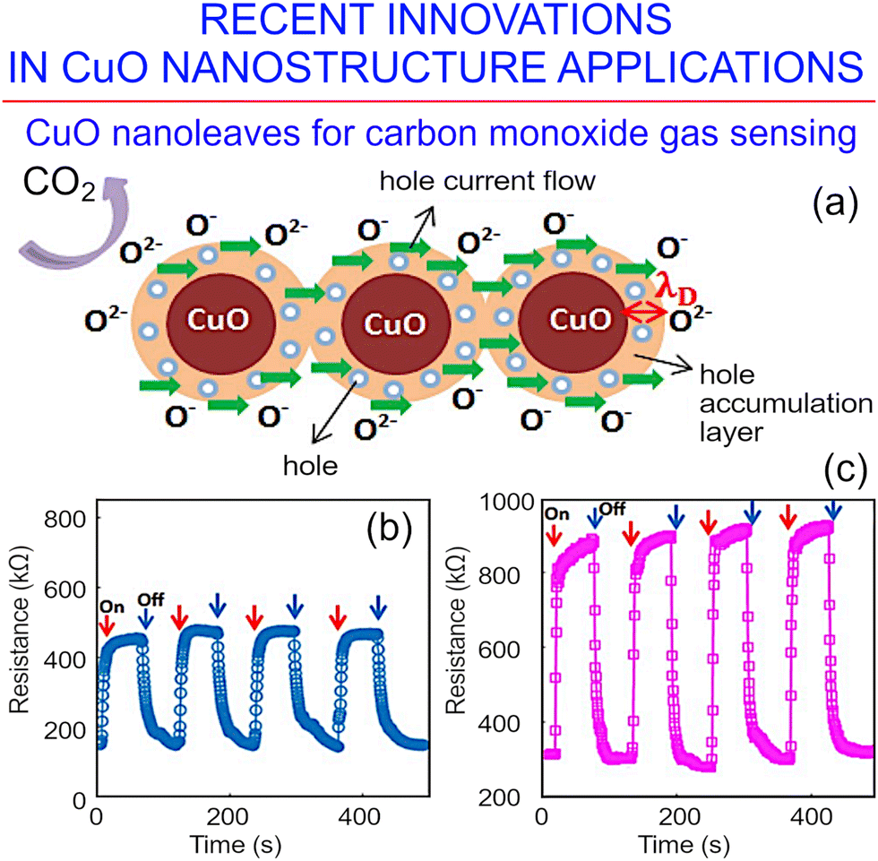 | ||
| Fig. 18 Carbon monoxide sensor. (a) Principle of the sensing mechanism of copper oxide for carbon monoxide utilizing a hole accumulation layer. (b and c) Repeated response to 800 ppm carbon monoxide for (b) pure CuO sensors; and (c) Al doped CuO sensors when operated at their optimum temperature of 120 and 150 °C, respectively. Reprinted with permission from Molavi et al., ref. 153. Copyright 2020, Elsevier. | ||
Finally, Hao et al. modified Cu NWs by depositing them on top of graphene oxide nanosheets to obtain a sensor for multiple simultaneous uses, such as in the detection of ascorbic acid, dopamine, and acetaminophen.155Fig. 19a presents a schematic of analyte gas molecule adsorption on the CuO/rGO hybrid surface. The novel copper oxide/functionalized graphene hybrid nanostructures were fabricated for gas sensing.154Fig. 19b shows the sensing response curve of a quartz crystal microbalance gas sensor with the CuO/rGO hybrid.
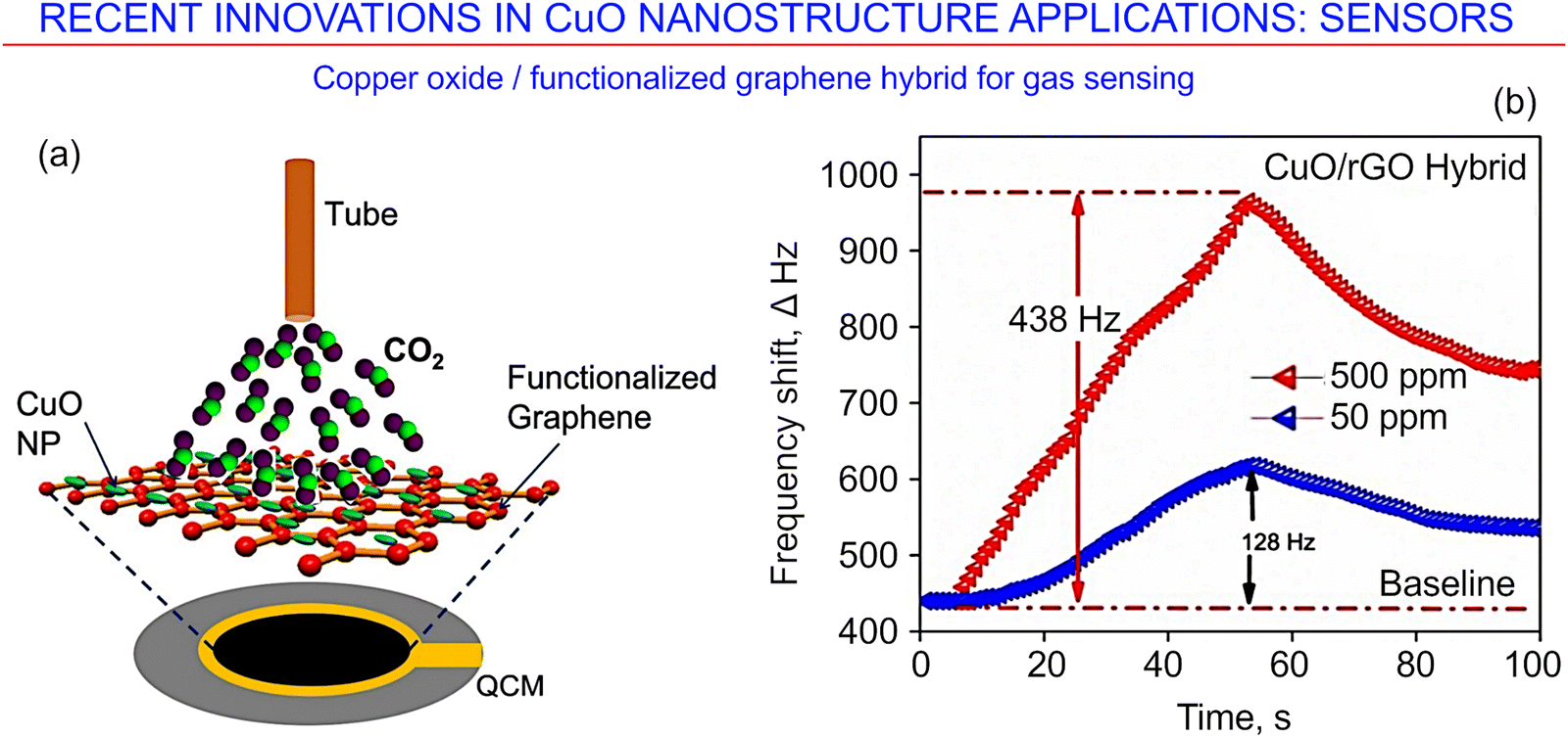 | ||
| Fig. 19 Copper oxide/functionalized graphene hybrid for CO2 gas sensing. (a) Schematic of analyte gas molecule adsorption on the surface. (b) Sensing response curve of the quartz crystal microbalance. Reprinted from Gupta et al. 2022, ref. 154 under terms and conditions of CC BY license. | ||
3.2. Innovations in CuO nanostructure-based metamaterials for biosensing
Biosensing is a very important area of application where CuO-based nanostructures and metamaterials ensure excellent results. CuO-based nanostructures were used recently for the fabrication of quite different biosensors156 that are capable of detecting neuromodulatory molecules such as dopamine,157,158 as well as active substances that are important for living beings, e.g., glucose, cysteine, carbon monoxide, hydrogen peroxide and others. Below we provide a brief overview of some of the recent innovations in copper oxide-based biosensor technology.A colorimetric visual biosensor for detecting L-cysteine has recently been synthesized using dopamine-coated copper oxide nanoparticles. This innovative approach is based on the use of natural dopamine, an organic molecule from the catecholamine and phenethylamine families and a neuromodulator, the chemistry of which is frequently used for the surface functionalization of copper oxide particles to improve their stability and sensitivity to L-cysteine (Fig. 20a).158 As a semi-essential amino acid that plays an important role as a building block in protein synthesis, L-cysteine occurs at intracellular concentrations of 20–200 μM in biosystems.159 The dopamine-coated copper oxide nanoparticles (CuO@DOP NPs) were fabricated using microwave radiation (operating parameters: 800 W, 2450 MHz). The actual suitability of the newly developed sensor for the detection of L-cysteine was ascertained by using it to analyse clinical samples of blood serum and urine. Fig. 20b shows the representative fluorescence emission spectra of the dopamine-coated copper oxide nanoparticles as a function the L-cysteine concentration. The authors conclude that a sensor based on such dopamine-coated copper oxide nanoparticles may be used for the detection of L-cysteine both rapidly and with a high level of sensitivity across a broad range of concentrations, while being biocompatible with living systems.
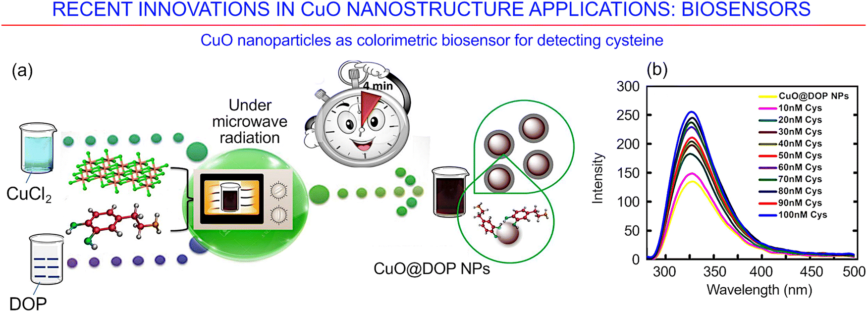 | ||
| Fig. 20 CuO nanomaterial-based biosensor. (a) CuO nanoparticles as a colorimetric biosensor for detecting cysteine, and (b) fluorescence spectra as a function of the wavelength for dopamine-coated copper oxide nanoparticles, for different concentrations of L-cysteine. Reprinted with permission from Rohilla et al., ref. 158. Copyright 2020, Elsevier. | ||
Nanostructures with interesting and very promising properties were recently reported by Cheng et al.160 Mesoporous hollow CuO spheres were fabricated and tested for use in paper-based hydrogen peroxide sensors, where the research was stimulated by the increasing demand for reliable, convenient and cheap paper-based sensors for the rapid detection of hydrogen peroxide in clinical, personal and industrial settings. Fig. 21a illustrates the schematic for the fabrication of hollow mesoporous CuO sphere nanozymes. The latter were fabricated by decomposing spherical copper–polyphenol colloidal particles. The resulting spherical structures were uniform in size (at ∼100 nm) and hollow, and featured an impressive specific surface area that reaching about 58 m2 g−1, with significant (about 0.5 cm3 g−1) porosity, and interconnected mesopores reaching diameters of 5.8 nm.
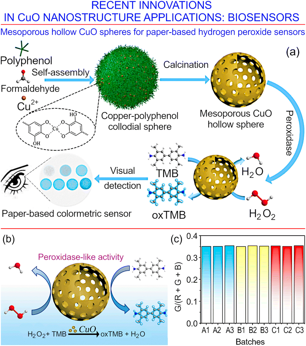 | ||
| Fig. 21 Mesoporous hollow CuO spheres for paper-based hydrogen peroxide sensors. (a) Schematic of the fabrication of hollow mesoporous CuO sphere nanozymes, and the application of this material as a paper-based sensor for the colorimetric detection of hydrogen peroxide. (b) Schematic of the detection mechanism for hydrogen peroxide by the hollow mesoporous CuO sphere nanozymes. (c) Measurement repeatability for three batches of the paper-based sensors towards the detection of hydrogen peroxide. Reprinted with permission from Cheng et al. 2021, ref. 160 under terms and conditions of CC BY license. | ||
Fig. 21b shows a schematic of the detection mechanism for hydrogen peroxide by the hollow mesoporous CuO sphere nanozymes. The sensors demonstrated an excellent peroxidase-detection activity as well as detection repeatability, as illustrated in Fig. 21c. They can be used for the colorimetric detection of peroxidase in the concentration range of 2.4–150 μM.
A method for the fabrication of hydrogen peroxide sensors using a simple polyol method, where copper oxide particles are produced when copper(II) acetate is hydrolyzed in 1,4-butanediol in the absence of additives, was also reported recently.161Fig. 22 illustrates the general approach for the synthesis of the copper oxide nanoparticle (CuONP)-based non-enzymatic electrochemical sensor. The authors simply drop-cast the sensing CuONP nanomaterial onto a glassy carbon electrode (GCE) which was modified using the poly(3,4-ethylenedioxythiophene) (PEDOT) conducting polymer. The latter was formed as a layer on a glassy carbon electrode via a sinusoidal voltage method.
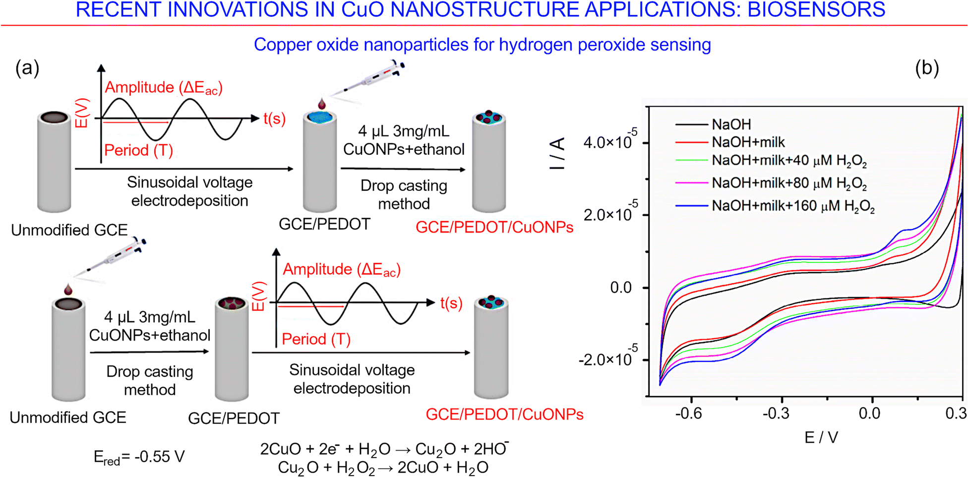 | ||
| Fig. 22 Copper oxides for biosensing. (a) Approach for the synthesis of a copper oxide nanoparticle (CuONP)-based non-enzymatic electrochemical sensor for the detection of hydrogen peroxide. (b) Cyclic voltammetry results for the sensor based on GCE/PEDOT-CuONPs when used to detect different amounts of hydrogen peroxide in a diluted milk sample. Reprinted with permission from Lete et al. 2022, ref. 161 under terms and conditions of CC BY license. | ||
The formation of nanoparticles assembled into quasi-prismatically-shaped microscale aggregate structures with sizes in the range from 1 μm to ∼200 μm, characterized by a mesoporous structure, was reported recently. Furthermore, the newly designed electrochemical sensing platforms appear to respond linearly with an increase in the hydrogen peroxide concentration from 0.04 to 10 mM, and have a low threshold (about 8.5 μM) for peroxide detection. Importantly, the sensing platform features very good anti-interference characteristics when substances, e.g., potassium nitrate and potassium nitrite, which are known to interfere with the detection of hydrogen peroxide, are present.
In addition to detecting biomolecules, copper oxide-based biosensors may be useful in the detection of viral protein structures for both health and environmental applications.162 Viral infections can spread rapidly amongst human, animal and plant populations, and their timely detection is often critical to limit their spread and develop a treatment plan. Amongst the most prominent examples of this are the human immunodeficiency virus (HIV), the Ebola virus, and, most recently, COVID-19. The polymerase chain reaction (PCR) is currently the most reliable technology used to determine the identity of a virus; however, its use is limited by its high cost and the length of time it takes to produce the answer, especially when demand for the service is high. To circumvent these limitations, a new generation of sensors is needed. An example of such a sensor was recently developed using a graphite electrode decorated with CuO nanostructures deposited via wet chemical processing. The antibody corresponding to the nucleocapsid protein of the SARS-CoV-2 virus was immobilized on the CuO–graphite electrode structure, where the N protein is an abundant RNA-binding protein that plays an important role in genome packaging in viruses. The antigen–antibody interaction was confirmed using square wave voltammetry (SWV). Fig. 23a illustrates the fabrication technology and explains the main steps, and Fig. 23b shows stronger performance brought about when graphite electrodes are modified with both hydroxyapatite (HAP) and copper oxide (CuO), compared with a pure graphite electrode or that modified with HAP alone.
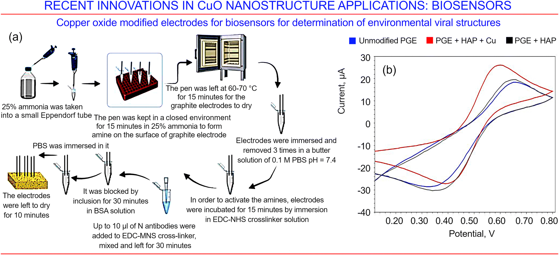 | ||
| Fig. 23 Copper oxides for biosensing. (a) Functionalization of pen shaped graphite electrodes endowed with hydroxyapatite and copper oxide carrying a nucleocapsid of COVID-19 antibody, and an illustration of the main pathways in the preparation of the electrochemical sensor based on copper oxide. (b) Results from cyclic voltammetry applied to untreated and treated pen shaped graphite electrodes with hydroxyapatite and copper oxide for a solution of 2.0 mM FeCl3 in 1.0 M HCl using a 10 mV s−1 scanning rate. Reprinted with permission from Ekici et al. 2022, ref. 162 under terms and conditions of CC BY license. | ||
3.3. Innovations in CuO nanowire-based metamaterials for glucose detection
The quick and reliable detection of glucose remains a very important challenge as the incidence of diabetes is increasing at an unprecedented rate all over the globe. At present, close to half a billion people on the planet suffer from this chronic condition, as estimated by the World Health Organization, while only about one hundred million cases were registered in 1980. Our ability to deal with this disease relies on the availability of devices and technologies for the accurate, reproducible and rapid detection of glucose concentrations of in a variety of media, from patient blood to food and medication that the patient may be consuming. Unfortunately, the currently available sensors for glucose detection are limited by their use of high-cost enzymes, and the results that they produce are insufficiently reproducible. As a consequence, efforts have been made to develop cheaper non-enzymatic sensors with both high selectivity and sensitivity.163Baek et al.164 proposed a novel electrospinning method for the fabrication of a graphene-based oxide nanofiber decorated with Cu-nanoflowers to be employed as an electrochemical biosensor for glucose detection (Fig. 24). Chen et al.165 fabricated an NO2 sensor using gold-functionalized CuO nanorods via a hydrothermal process at a room temperature. The resulting CuO nanorods had a diameter of 30–60 nm and a length of 150–200 nm, and displayed a robust structure that was not affected by the Au functionalization process used. It was found that small Au nanoparticles, with a diameter smaller than about 20 nm, were quite uniformly distributed over the surface. The authors concluded that the observed enhanced sensing characteristics were due the increased number of oxygen vacancies as well as to the lower activation energy as a result of Au functionalization. Lee et al.166 developed a network of p-CuO NWs grown on a predefined electrode pad pattern via the thermal oxidation of a Cu layer deposited using an electron-beam. Heat treatment of the Au layer, deposited by sputtering, was used to functionalize the Au nanoparticles. The latter had a diameter in the range of 20–145 nm, obtained by controlling the deposited Au layers thickness. It was found that Au functionalization enhanced the sensitivity of the CuO nanowires to a large extent, yielding the best sensing characteristics after functionalization with 60 nm-diameter Au NPs. One may conclude that, for functionalization to be efficient, the size optimization of the nanoparticles is very important to ensure the superior sensing characteristics of the oxide nanowires. Indeed, the response for CO was improved by approximately a factor of two compared with the traditional method using benzene and toluene.
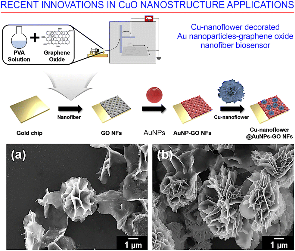 | ||
| Fig. 24 Electrochemical biosensor for glucose detection. (Upper panel) Synthesis of copper (Cu)-nanoflowers, decorated on graphene oxide (GO) nanofibers with gold nanoparticles, as an electrochemical biosensor for the detection of glucose. (Bottom panels) Optimization of the Cu-nanoflower at different GO concentrations: (a) 0.3 mg mL−1, and (b) 0.5 mg mL−1. Reprinted with permission from Baek et al., ref. 164. Copyright 2021, Elsevier. | ||
Nanowires with high aspect ratios were reported by Hadiyan et al.167 Cu2O NWs of 180 nm in diameter and 8 μm in length were synthesized via electrodeposition onto a polycarbonate substrate immersed in an aqueous solution. Further annealing yielded CuO/Cu2O composite NWs. They found that, at 250 °C, the Cu2O NWs work well as an accurate ethanol gas sensor, while their CuO/Cu2O counterparts also showed good sensing response for CO at 150 °C. These results indicate that the Cu2O NW gas sensor is almost six times faster than sensors designed using CuO/Cu2O nanowires. A comprehensive analysis conducted by Qi et al.168 on CO oxidation both in oxygen-rich and in hydrogen-rich atmospheres demonstrated that the CuO species play a major role in the oxidation of CO, consistent with the fact that the superior Au/CuO catalyst relies on its strong interaction with the substrate gold nanoparticles.
An excess glucose concentration in human blood can have a negative impact on human health. Therefore, people are actively working on the issue of detecting blood glucose contaminants in the human body, which can be an important indicator of the surge of diabetes. A complex copper oxide/zinc oxide nanostructured material for non-enzymatic glucose sensing was reported recently by Cheng et al.171 Electrodes were fabricated via a simple solution method, i.e., by the immersion of ZnO nanostructures into copper ion solutions. Tetrapod-like ZnO nano-powders were first obtained using a direct current plasma method, and the resulting surface was uniformly decorated with CuO nanocrystalline particles (Fig. 25a). Fig. 25b and c illustrate the response of the fabricated sensor to glucose.
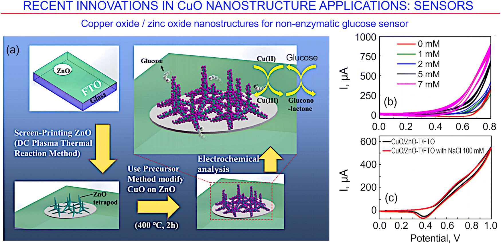 | ||
| Fig. 25 Copper oxide/zinc oxide nanostructures for a non-enzymatic glucose sensor. (a) Schematic of the fabrication process. (b) Current–voltage curves for glucose at various concentrations, and (c) response of the sensor to glucose solution. Reprinted from Cheng et al. 2021, ref. 171 under terms and conditions of CC BY license. | ||
In the interesting work by Patil et al., thin CuO films synthesized via chemical bath technology were reported.169 They found that thin films feature a much stronger response to glucose, in comparison with their response to ascorbic acid. The work by Steinhauer reviewed the recent achievements in designing novel devices using copper oxide nanomaterials, and discussed the key factors that determine the sensing characteristics and efficiency.170
Recently, an interesting electrodeposition approach was demonstrated to design ultrasensitive amperometric non-enzymatic glucose biosensors that use a more complex architecture, i.e., magnetically active thiol-functionalized Fe3O4–SH over a glassy carbon substrate, decorated with honeycomb-like copper oxide onto which silver nanoparticles are immobilized.172Fig. 26a illustrates the electrode structure that incorporates all of these elements, and Fig. 26b shows the cyclic voltammograms of glucose in NaOH for the bare electrode and for various CuO-honeycomb-supported systems. The thus-fabricated sensors show excellent sensitivity for glucose and a stability of response over a broad range (0.06–1000 mM) of glucose concentrations, with a detection threshold of 15 nM. As such, these sensors could potentially be used to detect glucose reliably in blood and urine clinical samples.
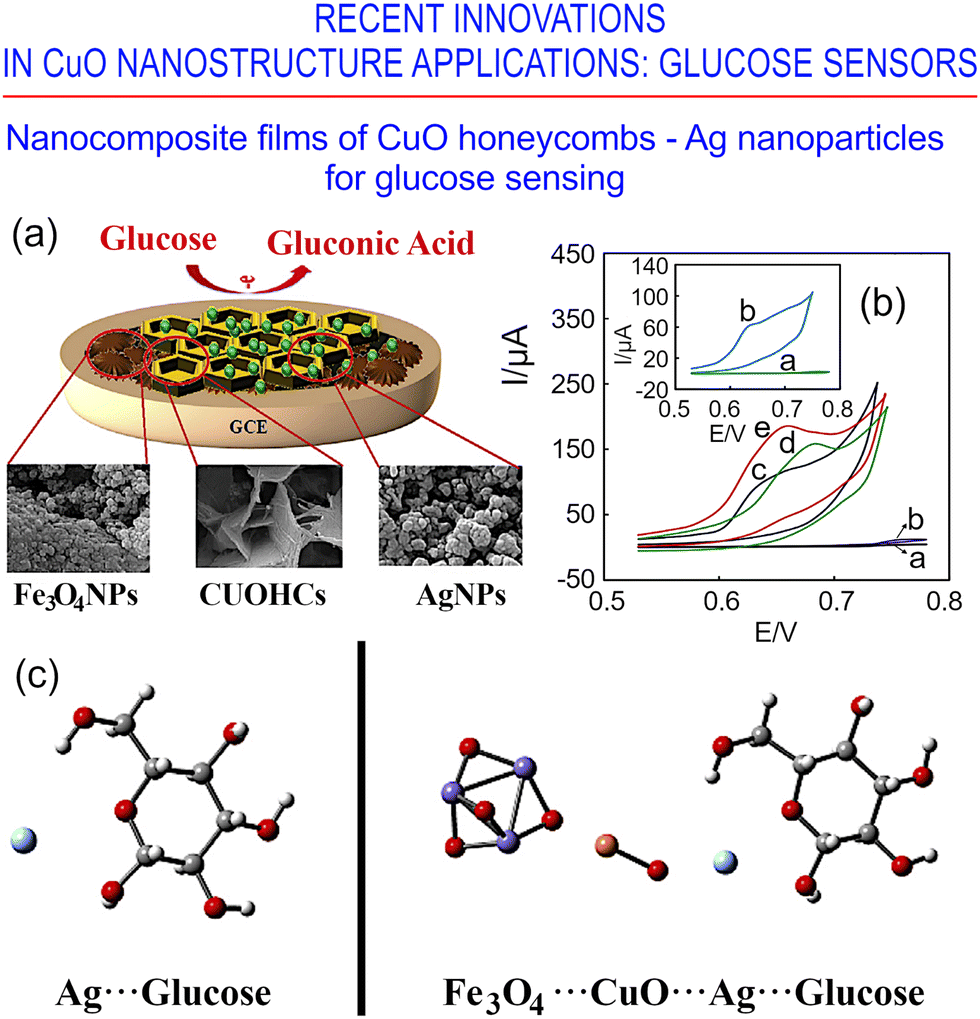 | ||
| Fig. 26 CuO honeycombs and nanoleaves for glucose and carbon monoxide sensing. (a) Electrode fabricated on nanocomposites of CuO honeycombs/Ag nanoparticles. (b) Cyclic voltammograms, for 0.1 mM glucose in 0.1 M NaOH solution, on various electrodes, including a bare electrode and various CuO-honeycomb-supported systems (see the details about traces labelled a–e in the original publication). (c) Optimized structures of the complexes: Ag⋯glucose and Fe3O4/CuO/Ag⋯glucose. Reprinted with permission from Baghayeri et al., ref. 172. Copyright 2020, Elsevier. | ||
One more technology for the fabrication of copper oxide-based biosensors for non-invasive glucose detection was developed recently by Franco et al.173 In order to fabricate the sensor, the authors first print-coated electrodes onto fabric that was made of cellulose using a paste containing graphene. Cellulose is an excellent substrate material as it offers an attractive combination of minimal cost and toxicity, abundance, excellent compatibility with living systems, the ability to be disposed of and degrade naturally, as well as excellent porosity that maximises the contact area between the sensor and the biofluid. Drop-casting was then carried out to deposit Cu2O nanoclusters onto the surfaces of the graphene electrodes, with the Cu2O crystals synthesized via an ascorbic acid reduction method. The sensing was made possible by exploiting electron transfer from copper oxide in an aqueous solution of sodium hydroxide and artificial sweat that takes place at a considerably low potential of +0.35 V, with the existence of the reduction–oxidation reaction between glucose and the nanoparticles confirmed using cyclic voltammetry and other characterization methods.
Fig. 27a illustrates the simplicity of this fabrication technology, which makes it highly attractive for the large-scale production of cheap disposable sensors that at the same time demonstrate a high level of sensitivity and reproducibility. The latter characteristics are shown in Fig. 27b for a NaOH solution with glucose levels ranging from 0.1 to 1 mM. Under these conditions, sensors based on copper oxide over a glassy carbon electrode show a sensitivity of about 1082 μA mM−1 cm−2, whereas those based on copper oxide nanoclusters over graphene electrodes (on cellulose) recorded a sensitivity of about 182 μA mM−1 cm−2. These measurements confirm the potential for these sensors to find applications in the non-invasive monitoring of patients with blood sugar disorders, particularly where portability improves patient uptake and compliance, as they show selectivity towards glucose in the presence of interfering urea and NaCl that are typically present in human sweat.
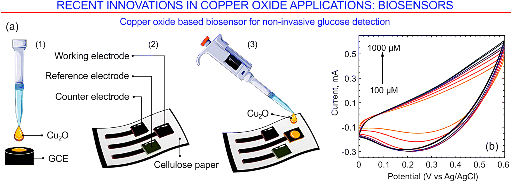 | ||
| Fig. 27 Copper oxide-based biosensor for non-invasive glucose detection. (a) General approach for the preparation of glucose-sensing platforms on a glassy carbon electrode (1; used for material characterization) and on a graphene electrode on a flexible glucose substrate (2–3; as a proof-of-concept study). Ag/AgCl is used as a pseudo-reference electrode. (b) Cyclic voltammetry curves for a sensor based on the Cu2O nanocluster-decorated graphene working electrode shown in (a3) for a glucose concentration in the range of 100 to 1000 μM in 0.1 M NaOH solution. Reprinted with permission from Franco et al. 2022, ref. 173 under terms and conditions of CC BY license. | ||
3.4. Innovations in CuO nanowire-based metamaterials for energy and catalysis
Many experiments have been published that report the use of gold as a metal nanoparticle source for the functionalization of CuO nanostructures. Efficient CuO photocathodes that feature remarkable stability were reported by Masudy-Panah et al.174 These authors exploited the novel engineering of in situ materials based on the deposition of gold–palladium (Au–Pd) nanoparticles on the surface of CuO. The basic functioning of these nanostructures relies on plasmonic centers which trap the incoming light, thus enhancing the optical absorption of the system. The associated hydrogen amount becomes larger than in the cases of bare CuO photocathodes.The results obtained by Sun et al. suggest that complex materials of hybridized cuprous sulfide and copper may play an important role in water splitting in pre-catalytic processes that do not use noble metals.85 Interestingly, the Cu2S particles evolved into CuO nanowires directly in the oxygen evolution reaction (OER). Similarly, nanostructures for the OER were reported by Butt et al., and the copper nanowires were fabricated via the reduction of CuO nanowires in hydrogen plasma.175 Testing this material for application in the hydrogen evolution reaction (HER) proved its exceptional characteristics, with the performance significantly exceeding the values obtained for the bulk copper material. Next, the complex CuO/Cu2O nanomaterial for Na+ ion storage was synthesized by Ma et al.176via the in situ modification of copper foam using the hydrothermal method (Fig. 28). The synergetic effect of CuO and Cu2O oxides can contribute to decreasing the volume change between the host materials, and, as a result, additional Na+ ions can be stored in the interfaces between the two oxides, leading to conspicuous capacity enhancements. The review by Majumdar et al.177 outlines the recent advancements in CuO-based nanosystems, which are typically employed for the design of better electrode materials aimed at developing advanced supercapacitors. In addition, they discuss the electrochemical responses for a variety of CuO nanostructures.
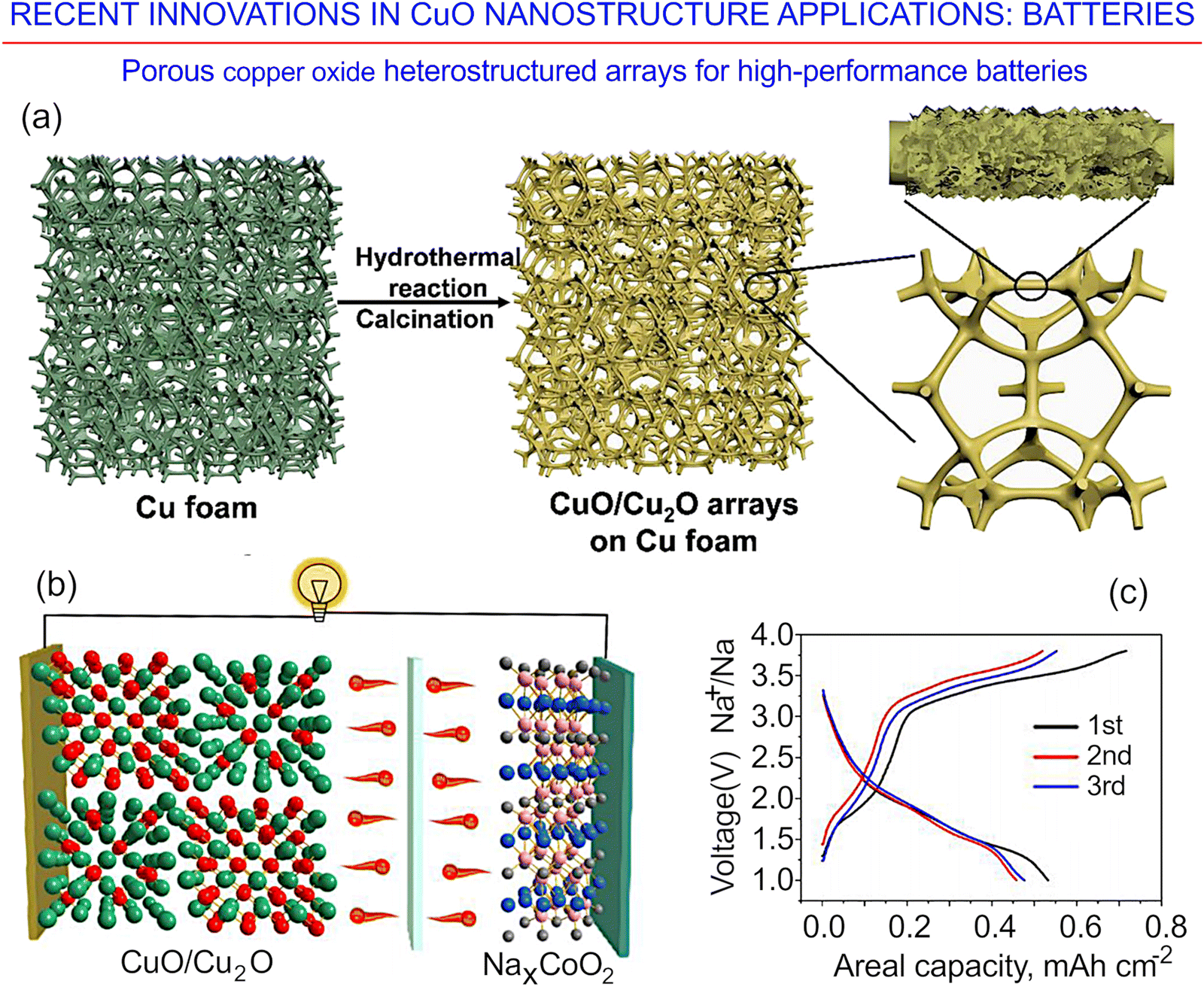 | ||
| Fig. 28 Porous copper oxide heterostructured arrays for high-performance batteries. (a) Synthesis of CuO/Cu2O arrays. (b) Full sodium-ion battery with a CuO/Cu2O anode and an NaxCoO2 cathode. (c) Initial three charge–discharge curves for a (CuO/Cu2O)–(NaxCoO2) full battery operating at a current density of 0.5 mA cm−2. Reprinted with permission from Ma et al., ref. 176. Copyright 2021, Springer. | ||
Pristine nanomaterials based on copper oxides feature a relatively low electrical conductivity and a rather low electrochemical stability. To overcome these and some other shortcomings, CuO nanomaterials could be combined with pseudo-capacitive materials such as, e.g., chalcogenide or carbon-containing materials like conductive polymers, graphene- and carbon nanotube-containing materials. A combination of CuO nanowires with graphene sheets was recently demonstrated to obtain highly porous, conductive hybrid nanomaterials that could be fruitfully employed as high-performance supercapacitor electrodes with enhanced capacitances (Fig. 29).178 Currently, the development of new technology based on high-performance nanoelectromechanical systems (NEMS) is limited by the problems associated with the synthesis of NEM switches based on single nanowires. A successful application of CuO nanowires as a NEM switch element was recently reported by Jasulaneca et al.179 Moreover, the anodized copper foams obtained by Abd-Elnaiem et al. have been to be an efficient material for enhancing the efficiency of organic dye decomposition.180
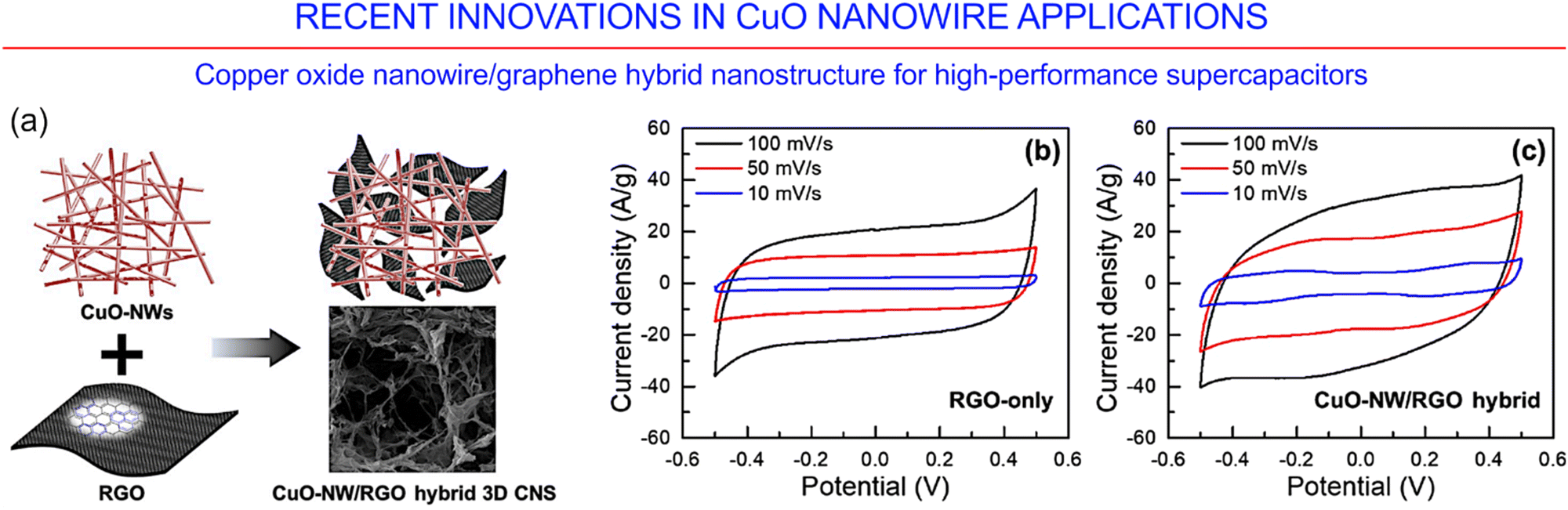 | ||
| Fig. 29 CuO-nanowire/reduced graphene oxide hybrid for high-performance supercapacitors. (a) Schematic of the CuO-nanowire/reduced graphene oxide hybrid three-dimensional carbon nanostructures. (b and c) Electrochemical current–voltage curves for RGO-only and CuO-nanowire/reduced graphene oxide hybrid three-dimensional carbon nanostructures. Reprinted with permission from Luan et al., ref. 178. Copyright 2019, Elsevier. | ||
A number of experiments carried out to develop a method for the highly-controllable synthesis of nanostructures includes a stage achieves metal nanoparticle deposition. In the study reported by Kim et al., broadband absorbing surfaces for solar energy applications were developed on self-aggregated alumina nanowires.181 Excellent antibacterial activity was reported by Menazea et al. for the material based on graphene oxides with the gold and CuO nanoparticles.182 Sun et al. proved that the functionalization of transition metal surfaces, carrying dichalcogenide nanosheets, could be used to obtain better electrical contacts to devices, together with the improvement of their catalytic and sensing characteristics.183 Along this line of research, Attar at al.184 reported, for the first time, the high electrocatalytic performance of a carbon paste electrode modified by polypyrrole–copper oxide particles (Cu2O/PPy/CPE) for the electrocatalytic oxidation of ethanol.
Fig. 30a shows the technology for the fabrication of self-supporting electrodes for the oxygen evolution reaction and supercapacitors. By employing a facile electro-oxidation method, CuxO nanoflakes have been successfully grown in situ on a nanoporous Cu foil. In order to realize the formation of a nanoporous Cu layer on a flexible Cu foil, a Ga–Cu alloying/dealloying system prepared on a Ga-assisted surface was used. Electro-oxidation carried out at a constant potential was used to modify the nanoporous Cu layer containing the CuxO nanoflakes. The optimum electrode configuration was able to deliver a rather high areal capacitance of about 0.75 F cm−2 at a current density of 0.2 mA cm−2. The samples were able to maintain about 95% of the capacitance through 12000 cycles. The supercapacitor built using CuxO/Cu as the positive electrode and activated carbon as the negative electrode demonstrated energy and power densities of 24.2 W h kg−1 and 0.65 kW kg−1, respectively.185
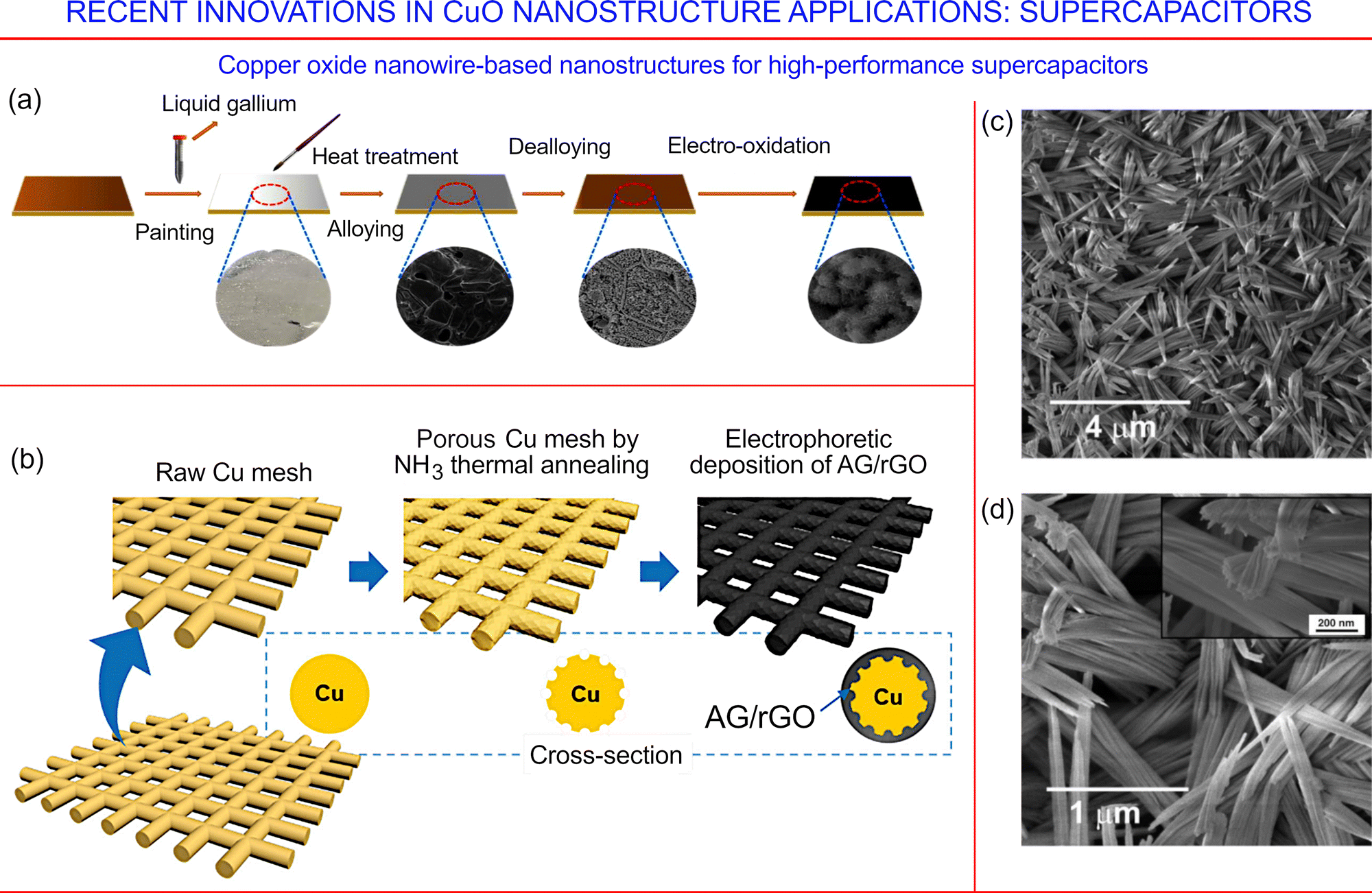 | ||
| Fig. 30 (a) Fabrication process of the CuxO/Cu electrodes. Reprinted from Li et al. 2022, ref. 185 under the terms and conditions of the CC BY license. (b) Fabrication of activated graphene (AG)/reduced graphene oxide (rGO) deposited on a porous Cu (P-Cu) mesh. Reprinted from Lim et al. 2021, ref. 186 under the terms and conditions of the CC BY license. (c and d) Morphology of anodic CuO/Cu2O nanoneedles obtained for Cu foils anodized in KOH–H2O–NH4F electrolyte. Inset in (d) is a high-magnification SEM image. Reprinted from Oyarzún et al. 2021, ref. 187 Copyright under the terms and conditions of the CC BY license. | ||
Another technology for CuO-based supercapacitors has been reported recently by Lim et al., in which a porous Cu mesh was implemented as the current collector, while a porous surface was made via thermal annealing of the Cu mesh in an ammonia gas environment.186 Activated graphene, with a hierarchical porous distribution and a high specific surface area, and graphene oxide were deposited onto the porous Cu substrate via electrophoretic deposition. Subsequently, the graphene oxide was transformed into electrically conductive rGO. This material yielded a high specific capacitance reaching 140 F g−1, together with a prominent energy density exceeding 3 W h kg−1 (Fig. 30b). Fig. 30c and d show SEM images of the anodic CuO/Cu2O nanoneedles obtained for Cu foils anodized in KOH–H2O–NH4F electrolyte.187
✓ Thus, various types of CuO nanostructures with low dimensionality could be successfully implemented for advanced applications in sensing, energy and catalysis, as follows from the recent achievements (mostly 2021 and 2022) reviewed above. Apparently, this material still holds great potential for future developments, and more effort should be devoted to the design of novel, complex, hierarchical materials and metamaterials for advancing future applications.
✓ However, apart from the above outlined sensing, energy and catalysis applications, CuO nanostructures with low dimensionality could also be implemented in other leading-edge applications, such as space exploration and medicine. In the Outlook section below we will briefly discuss these novel areas of application for CuO nanostructures.
✓ Furthermore, some further problems and open questions related to the CuO nanostructures will be outlined in the Outlook section.
4. Outlook
Diversity of technologies and applications for CuO-based low-dimensional nanostructures
The above-reviewed recent results on the development of fabrication technologies and advanced applications of CuO-based low-dimensional nanostructures demonstrate a flourishing diversity of techniques and devices that utilize CuO-containing materials. Importantly, many types of complex, hierarchical materials systems and metamaterials could be built using CuO-based low-dimensional nanostructures. The spectrum of recently reported morphologies and applications of low-dimensional CuO nanostructures, as examined in this review, is presented in Fig. 31. To get a better overview of this diversity and thus to stress the greatest potential of CuO-based low-dimensional nanostructures for future applications, we have compiled the general list in Table 1 that provides examples that have been discussed in detail in this review.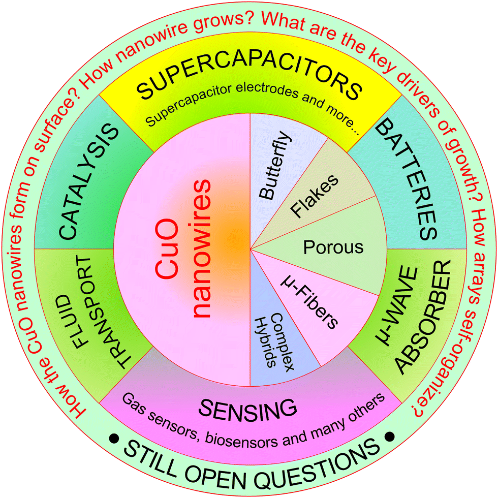 | ||
| Fig. 31 Spectrum of recently reported morphologies and applications of low-dimensional CuO nanostructures examined in this review. While energy, sensing and catalysis could be considered as the ‘classic triad of applications’ for CuO nanomaterials, other applications have also been the focus of recent investigations. By contrast, nanowires and large organised arrays of CuO nanowires are the most common form of CuO nanomaterials for advanced applications, but other morphologies including quite exotic forms, such as butterfly-like nanostructures, have also been the subject of focus. Besides, in spite of great advances achieved in the synthesis and applications of CuO nanomaterials for advanced applications and theoretical insights in the growth mechanisms, some questions are still remain, as highlighted within this scheme, with the most intriguing queries being “What are the key drivers of growth?” and “How arrays of CuO nanowires self-organize during growth on the surface?”. | ||
| Type of nanostructure | Fabrication process | Feature of process/product | Potential application | Ref. |
|---|---|---|---|---|
| Nanowires | RFPE | Uniform surface growth | Sensing | 68 |
| Butterfly-like nanostructures | MAHT | CuO sheets were polarized by microwaves and arranged | Sensing | 69 |
| Nanowires | Thermal-induced | Electric-field assisted growth | Building blocks for nanodevices | 72 |
| Nanowires | MTO | Higher humidity produced higher yields of NWs | Nano-electro-mechanical systems | 73 |
| Porous hollow nanotubes | ES + TP | Nanotubes embrace copper oxide nanoparticles | Gas sensors | 75 |
| Nanowires | Plasma | Catalyst-free, single-crystalline | Sensing, catalysis | 74 |
| Nanowires | Facile solution-phase | Monoclinic polycrystalline structure | Sensors for volatile organic compounds | 77 |
| Nanowires | Anodization in sodium bicarbonate | Partial self-healing suggested | Various | 78 |
| Nanowires | Facile biosynthesis | Sapindus mukorossi fruit extract as a biosurfactant | Electrochemical sensing of dopamine | 79 |
| Nanowires | Thermal oxidation | Grown directly on V-shaped microgroves | Heat and fluid transport | 84 |
| Nanowires | Chemical synthesis | Cu2S nanoparticles evolved into CuO nanowires | Catalysis of water splitting | 85 |
| Nano-needle arrays | Magnetron sputtering + wet etching + annealing | Grown on commercial ceramic tube | Tube-like gas sensors | 113 |
| Nanowires-3D copper hybrid | Electroless deposition | Hybrid with gold nanoparticles and CuxO nanowire-3D copper | Various | 128 |
| Graphene-based oxide nanofiber | Electrospinning | Decorated by Cu-nanoflowers | Biosensor for glucose | 164 |
| Complex nanomaterial | DC plasma thermal reaction method | Uniformly decorated by CuO nanocrystallines | Non-enzymatic glucose sensor | 171 |
| CuO/graphene | Reduction in ascorbic acid | Enriched with oxygen functional groups and defective sites | Gas sensing | 154 |
| Porous copper oxide | Hydrothermal reaction, calcination | Porous copper oxide heterostructured arrays | High-performance batteries | 176 |
| Nanowires | Reduction, oxidation | Synergetic combination of nanowires and graphene sheets | High-performance supercapacitors | 178 |
| CuxO nanoflakes | Facile electro-oxidation | Nanoporous Cu layer on flexible Cu foil | High-performance supercapacitors | 185 |
| Porous mesh | Thermal annealing | Activated/reduced graphene oxide on porous Cu | High-performance supercapacitors | 186 |
| Microfibers | Thermal annealing | C/CuO microfiber composites | Microwave absorbance | 193 |
| CuO/Cu2O nano-needles | Electrophoretic deposition | Hierarchical porous distribution | High-performance supercapacitors | 187 |
From this table one can see that the most commonly discussed CuO nanostructures are nanowires, while some unique shapes, such as butterfly-like nanostructures, porous hollow nanotubes, nano-needle arrays, CuxO nanoflakes, porous mesh and microfibers, have also been created and successfully tested for applications in the past 2 years. Complex CuO/graphene and CuO/rGo nanostructured materials are also promising for various applications. Regarding the fabrication techniques, both plasma-based/electric field-assisted methods and thermal-type technologies are promising and are currently under development (Table 1). Microwave and radio-frequency plasmas are among the most promising techniques, although simple, cheaper DC-current plasma systems are also efficient for the fabrication of various CuO nanostructures and metamaterials.
Electric transport in copper oxide nanostructures
Despite the great diversity of CuO-based nanomaterials, electric field- and electric current-related phenomena play very important roles in most of their applications. As a result, a deep knowledge of the properties of single nanostructures or building blocks is of primary importance for understanding the fundamental issues of the device and its final performance. Unsurprisingly, many recently published reports discuss the electric field- and electric current-related phenomena in CuO-based nanomaterials. Recently, Kajli et al.188 reported anomalies in the current density of copper oxide nanowires grown via a thermal process, i.e., the current was observed to decrease as a function of the nanowire diameter. As shown via Raman and photoluminescence characterization, this behavior can be traced to the presence of (hole) traps in thicker Cu2O NWs that hinder charge transport in p-type CuO. Quantum confinement has been reported by Ghosh et al.189 for chemically synthesized freestanding thin (about 3–4 nm) CuO nanosheets at room temperature. Due to quantum confinement effects, the nanosheets displayed a rather large band gap of about 2.1 eV, larger than that for bulk CuO. These results point to the usefulness of these materials in supercapacitor devices. Shariffar et al. developed a UV-visible photodetector, based on copper oxide thin films, that displays enhanced optoelectronic properties if the films are synthesized at higher temperatures.190 Such behavior could be explained by the grain-structure model. Further investigations revealed the influence of the grain size on the photocurrent, dark current, photosensitivity and responsivity. Zhou et al. also confirmed that the nanomaterial morphology has a major effect on the observed properties and types of application.191 They found that CuO nanostrip sensors possess a larger surface area and faster electron transfer compared with CuO nanowires and/or microspheres. They also displayed the superior electrochemical sensing of glucose and tetrabromobisphenol. As a result, one may expect that the morphology of CuO nanomaterials can influence the performance of devices that are based on these nanomaterials.192Other applications of CuO-based nanostructures
CuO-based nanostructures could be promising for many advanced applications that are not currently mature, e.g., for space exploration. Light, thin, microwave-absorbing materials could be prepared using carbon/CuO microfiber composites, as was demonstrated recently (Fig. 32).193 Protective materials of this type would be indispensable for human protection in space and in other harsh environments. Moreover, CuO-based nanostructures could be a base for cold electron emitters, capable of enhancing the characteristics of space propulsion systems.194–197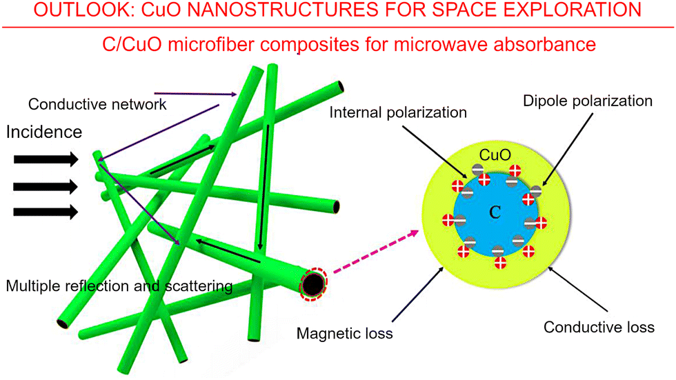 | ||
| Fig. 32 Novel materials based on CuO nanostructures for possible space exploration applications. Mechanism of microwave energy absorbance on C/CuO microfiber composites. Reprinted with permission from Wei et al., ref. 193. Copyright 2021, Springer. | ||
Apart from the energy, sensing and catalysis applications discussed in this review, biomedical applications are among the most important fields that directly influence human health and wellbeing. Low-dimensional CuO-based nanostructures are quite promising for many biomedical applications that include, but are not limited to, e.g., glucose sensing, H2O2 sensing, immunosensing, dopamine sensing, targeted cancer therapy, microbial warfare agents, wound healing and others (Fig. 33). While these applications are outside the scope of our review, we stress here in the Outlook the importance of biomedical applications, with a view to promoting further research activities in the field of bioactive low-dimensional copper oxide materials.
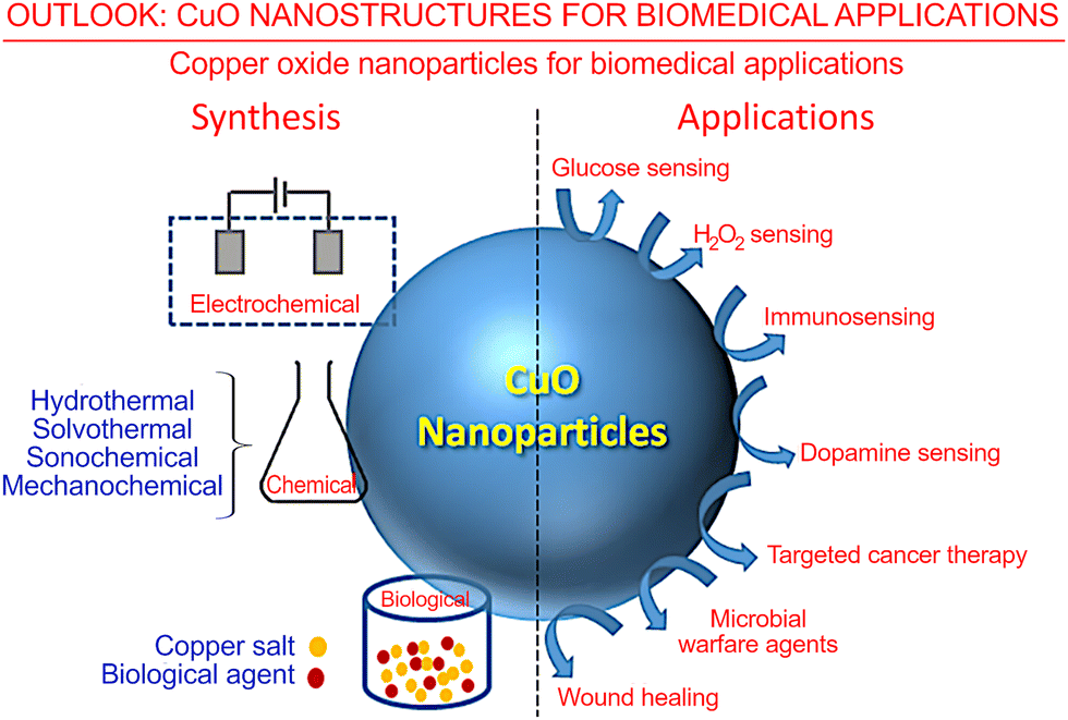 | ||
| Fig. 33 Copper oxide nanoparticles for future biomedical applications. Low-dimensional CuO-based nanostructures are quite promising for many biomedical applications that include, but are not limited to, e.g., glucose sensing, H2O2 sensing, immunosensing, dopamine sensing, targeted cancer therapy, microbial warfare agents, wound healing and others. Reprinted with permission from Verma et al., ref. 198. Copyright 2019, ACS. | ||
Future trends and tasks
Recently (2020), a quite detailed and comprehensive review on CuO-based nanomaterials for gas sensing was presented, where several points were outlined as directions for the future research.69 Based on newly achieved results and the broader scope of our review, which outlines energy applications and various techniques for the fabrication of CuO-based nanomaterials, we further develop and widen here the points suggested by Li et al.:✓ loading CuO-based nanomaterials and nanostructures with noble metals and multiple doping with various elements is promising for many applications, and thus requires more research and design efforts;
✓ the interaction of CuO-based nanomaterials with various types of plasma is very important to deepen our understanding of the processes during the synthesis of various nano- and metamaterials;
✓ techniques for fabricating CuO-based nanomaterials in plasmas of various types should be further improved;
✓ in view of their relative simplicity, chemical and thermal methods for the fabrication of CuO-based nanomaterials are also very promising and should be further developed;
✓ further progress is required for understanding the routes and driving forces of the low-dimensional growth of nanomaterials;
✓ numerical simulations, in particular the artificial intelligence-based approaches, should be developed to ensure the deterministic design of CuO-based nanomaterials.
Conclusions
In this review paper we have outlined the most recent progress (mostly within the past 2 years) in the synthesis and application of low-dimensional copper oxide nanomaterials and complex materials designed on the basis of CuO. Further directions are discussed, and the most pressing problems outlined.Conflicts of interest
There are no conflicts to declare.Acknowledgements
O. Baranov acknowledges the support from the project funded National Research Foundation of Ukraine, under grant agreement no. 2020.02/0119 and NATO Science for Peace and Security Programme under grant id: G5814 project NOOSE, whereas U. Cvelbar acknowledges the support from Slovenian Research Agency grants N2-0107, J2-4490 and program P1-0417. I. Levchenko acknowledges the support from the Nanyang Technological University, National Institute of Education. K. Bazaka acknowledges the support from the Australian Research Council (FT190100819) and The Australian National University Futures Scheme.References
- I. Levchenko, K. Bazaka, M. Keidar, S. Xu and J. Fang, Hierarchical multicomponent inorganic metamaterials: intrinsically driven self-assembly at the nanoscale, Adv. Mater., 2018, 30, 1702226, DOI:10.1002/adma.201702226.
- C. Piferi, K. Bazaka, D. L. D'Aversa, R. Di Girolamo, C. De Rosa, H. E. Roman, C. Riccardi and I. Levchenko, Hydrophilicity and hydrophobicity control of plasma-treated surfaces via fractal parameters, Adv. Mater. Interfaces, 2021, 8, 2100724, DOI:10.1002/admi.202100724.
- D. J. Wales, Dynamical signatures of multifunnel energy landscapes, J. Phys. Chem. Lett., 2022, 13, 6349–6358, DOI:10.1021/acs.jpclett.2c01258.
- L. Tu, Y. Xie and Z. Li, Advances in pure organic mechanoluminescence materials, J. Phys. Chem. Lett., 2022, 13, 5605–5617, DOI:10.1021/acs.jpclett.2c01283.
- S. Sasi, K. Prasad, J. Weerasinghe, O. Bazaka, E. P. Ivanova, I. Levchenko and K. Bazaka, Plasma for aquaponics, Trends Biotechnol., 2023, 41, 46–62, DOI:10.1016/j.tibtech.2022.08.001.
- A. Kumar, A. Aljumaili, O. Bazaka, E. P. Ivanova, I. Levchenko and K. Bazaka, Functional nanomaterials, synergism and biomimicry for environmentally benign marine antifouling technology, Mater. Horiz., 2021, 8, 3201–3238, 10.1039/D1MH01103K.
- M. Wagner, A. Seifert and L. M. Liz-Marzán, Towards multi-molecular surface-enhanced infrared absorption using metal plasmonics, Nanoscale Horiz., 2022, 7, 1259–1278, 10.1039/D2NH00276K.
- H. P. Zhou, X. Ye, W. Huang, M. Q. Wu, L. N. Mao, B. Yu, S. Xu, I. Levchenko and K. Bazaka, Wearable, flexible, disposable plasma-reduced graphene oxide stress sensors for monitoring activities in austere environments, ACS Appl. Mater. Interfaces, 2019, 11, 15122–15132, DOI:10.1021/acsami.8b22673.
- A. Mitra, M. R. Hermes, M. Cho, V. Agarawal and L. Gagliardi, Periodic density matrix embedding for CO adsorption on the MgO(001) curface, J. Phys. Chem. Lett., 2022, 13, 7483–7489, DOI:10.1021/acs.jpclett.2c01915.
- W. Shao, L. Zhang, Z. Jiang, M. Xu, Y. Chen, S. Li and C. Liu, Bioinspired conductive structural color hydrogels as a robotic knuckle rehabilitation electrical skin, Nanoscale Horiz., 2022, 7, 1411–1417, 10.1039/D2NH00322H.
- A. Imran, B. S. Moyer, A. J. Wolfe, M. S. Cosgrove, D. E. Makarov and L. Movileanu, Interplay of affinity and surface tethering in protein recognition, J. Phys. Chem. Lett., 2022, 13, 4021–4028, DOI:10.1021/acs.jpclett.2c00621.
- S.-J. Yang, Y.-K. Lin, Y.-C. Pu and Y.-J. Hsu, Crystal facet dependent energy band structures of polyhedral Cu2O nanocrystals and their application in solar fuel production, J. Phys. Chem. Lett., 2022, 13, 6298–6305, DOI:10.1021/acs.jpclett.2c01632.
- C. Zhang, Z. Peng, C. Huang, B. Zhang, C. Xing, H. Chen, H. Cheng, J. Wang and S. Tang, High-energy all-in-one stretchable micro-supercapacitor arrays based on 3D laser-induced graphene foams decorated with mesoporous ZnP nanosheets for self-powered stretchable systems, Nano Energy, 2021, 81, 105609, DOI:10.1016/j.nanoen.2020.105609.
- Z. Chen, S. Zhang, I. Levchenko, I. I. Beilis and M. Keidar, In vitro demonstration of cancer inhibiting properties from stratified self-organized plasma-liquid interface, Sci. Rep., 2017, 7, 12163, DOI:10.1038/s41598-017-12454-9.
- P. Liu, G. Wang, Q. Ruan, K. Tang and P. K. Chu, Plasma-activated interfaces for biomedical engineering, Bioactive Mater., 2021, 6, 2134–2143, DOI:10.1016/j.bioactmat.2021.01.001.
- K. Li, Y. de Rancourt de Mimérand, X. Jin, J. Yi and J. Guo, Metal oxide ZnO and TiO2 and Fe-Based metal–organic-framework nanoparticles on 3D-printed fractal polymer surfaces for photocatalytic degradation of organic pollutants, ACS Appl. Nano Mater., 2020, 3, 2830–2845, DOI:10.1021/acsanm.0c00096.
- Q. Xiang, X. Ma, D. Zhang, H. Zhou, Y. Liao, H. Zhang, S. Xu, I. Levchenko and K. Bazaka, Interfacial modification of titanium dioxide to enhance photocatalytic efficiency towards H2 production, J. Colloid Interface Sci., 2019, 556, 376–385, DOI:10.1016/j.jcis.2019.08.033.
- R. Réocreux, E. C. H. Sykes, A. Michaelides and M. Stamatakis, Stick or spill? Scaling relationships for the binding energies of adsorbates on single-atom alloy catalysts, J. Phys. Chem. Lett., 2022, 13, 7314–7319, DOI:10.1021/acs.jpclett.2c01519.
- Y. Xu, M. Fan, W. Yang, Y. Xiao, L. Zeng, X. Wu, Q. Xu, C. Su and Q. He, Homogeneous carbon/potassium-incorporation strategy for synthesizing red polymeric carbon nitride capable of near-infrared photocatalytic H2 production, Adv. Mater., 2021, 33, 2101455, DOI:10.1002/adma.202101455.
- X. Zhang and Y. Liu, Nanomaterials for radioactive wastewater decontamination, Environ. Sci.: Nano, 2020, 7, 1008–1040, 10.1039/C9EN01341E.
- I. Levchenko, M. Mandhakini, K. Prasad, O. Bazaka, E. P. Ivanova, M. V. Jacob, O. Baranov, C. Riccardi, H. E. Roman, S. Xu and K. Bazaka, Functional nanomaterials from waste and low-value natural products: a technological approach level, Adv. Mater. Technol., 2022, 7, 2101471, DOI:10.1002/admt.202101471.
- I. Levchenko, K. Bazaka, T. Belmonte, M. Keidar and S. Xu, Advanced materials for next generation spacecraft, Adv. Mater., 2018, 30, 1802201, DOI:10.1002/adma.201802201.
- I. Levchenko, M. Keidar, J. Cantrell, Y.-L. Wu, H. Kuninaka, K. Bazaka and S. Xu, Explore space using swarms of tiny satellites, Nature, 2018, 562, 185–187, DOI:10.1038/d41586-018-06957-2.
- N. Singhal, I. Levchenko, S. Huang, L. Xu, G.-C. Potrivitu, O. Cherkun, J. Fang, K. Bazaka and S. Xu, 3D-Printed multilayered reinforced material system for gas supply in cubeSats and small satellites, Adv. Eng. Mater., 2019, 21, 1900401, DOI:10.1002/adem.201900401.
- I. Levchenko, S. Xu, G. Teel, D. Mariotti, M. L. R. Walker and M. Keidar, Recent progress and perspectives of space electric propulsion systems based on smart nanomaterials, Nat. Commun., 2018, 9, 879, DOI:10.1038/s41467-017-02269-7.
- M. Hadiyan, A. Salehi and H. Mirzanejad, Gas sensing behavior of Cu2O and CuO/Cu2O composite nanowires synthesized by template-assisted electrodeposition, J. Korean Ceram. Soc., 2021, 58, 94–105, DOI:10.1007/s43207-020-00088-z.
- H. Xie, L. Zhu, W. Zheng, J. Zhang, F. Gao and Y. Wang, Microwave-assisted template-free synthesis of butterfly-like CuO through Cu2Cl(OH)3 precursor and the electrochemical sensing property, Solid State Sci., 2016, 61, 146–154, DOI:10.1016/j.solidstatesciences.2016.09.017.
- F. Shao, F. Hernández-Ramírez, J. D. Prades, C. Fàbrega, T. Andreu and J. R. Morante, Copper(II) oxide nanowires for p-type conductometric NH3 sensing, Appl. Surf. Sci., 2014, 311, 177–181, DOI:10.1016/j.apsusc.2014.05.038.
- F. Yang, J. Guo, M. Liu, S. Yu, N. Yan, J. Li and Z. Guo, Design and understanding of a high-performance gas sensing material based on copper oxide nanowires exfoliated from a copper mesh substrate, J. Mater. Chem. A, 2015, 3, 20477–20481, 10.1039/c5ta06806a.
- M. L. Zhong, D. C. Zeng, Z. W. Liu, H. Y. Yu, X. C. Zhong and W. Q. Qiu, Synthesis, growth mechanism and gas-sensing properties of large-scale CuO nanowires, Acta Mater., 2010, 58, 5926–5932, DOI:10.1016/j.actamat.2010.07.008.
- L. D. Duc, D. T. T. Le, N. Van Duy, N. D. Hoa and N. Van Hieu, Single crystal cupric oxide nanowires: length- and density-controlled growth and gas-sensing characteristics, Phys. E, 2014, 58, 16–23, DOI:10.1016/j.physe.2013.11.013.
- H.-W. Chang, S.-C. Chen, P.-W. Chen, F.-J. Liu and Y.-C. Tsai, Constructing morphologically tunable copper oxide-based nanomaterials on Cu wire with/without the deposition of manganese oxide as bifunctional materials for glucose sensing and supercapacitors, Int. J. Mol. Sci., 2022, 23, 3299, DOI:10.3390/ijms23063299.
- Q. Zhang, M. Li, Z. Wang, C. Qin, M. Zhang and Y. Li, Porous CuxO/Ag2O (x = 1, 2) nanowires anodized on nanoporous Cu–Ag bimetal network as a self-supported flexible electrode for glucose sensing, Appl. Surf. Sci., 2020, 515, 146062, DOI:10.1016/j.apsusc.2020.146062.
- S. Steinhauer, E. Brunet, T. Maier, G. C. Mutinati, A. Köck, O. Freudenberg, C. Gspan, W. Grogger, A. Neuhold and R. Resel, Gas sensing properties of novel CuO nanowire devices, Sens. Actuators, B, 2013, 187, 50–57, DOI:10.1016/j.snb.2012.09.034.
- Y. Feng and X. Zheng, Plasma-enhanced catalytic CuO nanowires for CO oxidation, Nano Lett., 2010, 10, 4762–4766, DOI:10.1021/nl1034545.
- V. Scuderi, G. Amiard, S. Boninelli, S. Scalese, M. Miritello, P. M. Sberna, G. Impellizzeri and V. Privitera, Photocatalytic activity of CuO and Cu2O nanowires, Mater. Sci. Semicond. Process., 2016, 42, 89–93, DOI:10.1016/j.mssp.2015.08.008.
- W. Wang, L. Wang, H. Shi and Y. Liang, A room temperature chemical route for large scale synthesis of sub-15 nm ultralong CuO nanowires with strong size effect and enhanced photocatalytic activity, CrystEngComm, 2012, 14, 5914–5922, 10.1039/c2ce25666e.
- W. N. Wang, F. Wu, Y. Myung, D. M. Niedzwiedzki, H. S. Im, J. Park, P. Banerjee and P. Biswas, Surface engineered CuO nanowires with ZnO islands for CO2 photoreduction, ACS Appl. Mater. Interfaces, 2015, 7, 5685–5692, DOI:10.1021/am508590j.
- L. Wang, K. Zhang, Z. Hu, W. Duan, F. Cheng and J. Chen, Porous CuO nanowires as the anode of rechargeable Na-ion batteries, Nano Res., 2014, 7, 199–208, DOI:10.1007/s12274-013-0387-6.
- Y. Su, T. Liu, P. Zhang and P. Zheng, CuO nanowire arrays synthesized at room temperature as a high-performance anode material for Li/Na-ion batteries, Thin Solid Films, 2019, 690, 137522, DOI:10.1016/j.tsf.2019.137522.
- B. J. Hansen, N. Kouklin, G. Lu, I. K. Lin, J. Chen and X. Zhang, Transport, analyte detection, and opto-electronic response of p-type CuO nanowires, J. Phys. Chem. C, 2010, 114, 2440–2447, DOI:10.1021/jp908850j.
- C. Tang, X. Liao, W. Zhong, H. Yu and Z. Liu, Electric field assisted growth and field emission properties of thermally oxidized CuO nanowires, RSC Adv., 2017, 7, 6439–6446, 10.1039/c6ra27426a.
- S. K. Shinde, H. M. Yadav, G. S. Ghogake, A. A. Kadam, V. S. Kumbhar, J. Yang, K. Hwang, A. D. Jagadale, S. Kumar and D. Y. Kim, Using chemical bath deposition to create nanosheet-like CuO electrodes for supercapacitor applications, Colloids Surf., B, 2019, 181, 1004–1011, DOI:10.1016/j.colsurfb.2019.05.079.
- G. Mahendra, R. Malathi, S. P. Kedhareswara, A. Lakshmi-Narayana, M. Dhananjaya, N. Guruprakash, O. M. Hussain, A. Mauger and C. M. Julien, RF sputter-deposited nanostructured CuO films for micro-supercapacitors, Appl. Nano, 2021, 2, 46–66, DOI:10.3390/applnano2010005.
- C. S. Lee and J. Bae, Room-temperature growth (“farming”) and high-performance supercapacitor applications of highly crystalline CuO nanowires/graphene nanoplatelet nanopowders, J. Mater. Sci.: Mater. Electron., 2018, 29, 15097–15105, DOI:10.1007/s10854-018-9650-7.
- K. Xu, H. Yan, C. F. Tan, Y. Lu, Y. Li, G. W. Ho, R. Ji and M. Hong, Hedgehog inspired CuO nanowires/Cu2O composites for broadband visible-light-driven recyclable surface enhanced Raman scattering, Adv. Opt. Mater., 2018, 6, 1701167, DOI:10.1002/adom.201701167.
- M. Al Ktash, M. Stefanakis, T. Englert, M. S. L. Drechsel, J. Stiedl, S. Green, T. Jacob, B. Boldrini, E. Ostertag, K. Rebner and M. Brecht, UV hyperspectral imaging as process analytical tool for the characterization of oxide layers and copper states on direct bonded copper, Sensors, 2021, 21, 7332, DOI:10.3390/s21217332.
- P. K. Amoah, M. Košiček, J. Perez, C. E. Sunday, S. Moreau, U. Cvelbar and Y. S. Obeng, Broadband microwave signal dissipation in nanostructured copper oxide at air-film interface, Electroanalysis, 2020, 32, 2795–2802, DOI:10.1002/elan.202060246.
- V. Shvalya, G. Filipič, D. Vengust, J. Zavašnik, M. Modic, I. Abdulhalin and U. Cvelbar, Reusable Au/Pd-coated chestnut-like copper oxide SERS substrates with ultra-fast self-recovery, Appl. Surf. Sci., 2020, 517, 146205, DOI:10.1016/j.apsusc.2020.146205.
- V. Shvalya, G. Filipič, J. Zavašnik, I. Abdulhalim and U. Cvelbar, Surface-enhanced Raman spectroscopy for chemical and biological sensing using nanoplasmonics: the relevance of interparticle spacing and surface morphology, Appl. Phys. Rev., 2020, 7, 031307, DOI:10.1063/5.0015246.
- C. Tang, X. Liao, W. Zhong, H. Yu and Z. Liu, Electric field assisted growth and field emission properties of thermally oxidized CuO nanowires, RSC Adv., 2017, 7, 6439–6446, 10.1039/c6ra27426a.
- Y. Su, T. Liu, P. Zhang and P. Zheng, CuO nanowire arrays synthesized at room temperature as a high-performance anode material for Li/Na-ion batteries, Thin Solid Films, 2019, 690, 137522, DOI:10.1016/j.tsf.2019.137522.
- C. S. Lee and J. Bae, Room-temperature growth (“farming”) and high-performance supercapacitor applications of highly crystalline CuO nanowires/graphene nanoplatelet nanopowders, J. Mater. Sci.: Mater. Electron., 2018, 29, 15097–15105, DOI:10.1007/s10854-018-9650-7.
- D. Majumdar and S. Ghosh, Recent advancements of copper oxide-based nanomaterials for supercapacitor applications, J. Energy Storage, 2021, 34, 101995, DOI:10.1016/j.est.2020.101995.
- S. Steinhauer, Gas sensors based on copper oxide nanomaterials: a review, Chemosensors, 2021, 9, 51, DOI:10.3390/chemosensors9030051.
- V. H. Luan, J. H. Han, H. W. Kang and W. Lee, Highly porous and capacitive copper oxide nanowire/graphene hybrid carbon nanostructure for high-performance supercapacitor electrodes, Composites, Part B, 2019, 178, 107464, DOI:10.1016/j.compositesb.2019.107464.
- A. Ghosh, M. Miah, A. Bera, S. K. Saha and B. Ghosh, Synthesis of freestanding 2D CuO nanosheets at room temperature through a simple surfactant free co-precipitation process and its application as electrode material in supercapacitors, J. Alloys Compd., 2021, 862, 158549, DOI:10.1016/j.jallcom.2020.158549.
- A. Shariffar, H. Salman, T. A. Siddique and M. O. Manasreh, Effects of high-temperature annealing on the performance of copper oxide photodetectors, Appl. Phys. A: Mater. Sci. Process., 2021, 127, 750, DOI:10.1007/s00339-021-04906-x.
- T. Ma, L. Gao, Y. Liu, L. Zhang and X. Yang, Porous CuO/Cu2O heterostructured arrays as anode for high-performance sodium-ion batteries, Ionics, 2021, 27, 1995–2003, DOI:10.1007/s11581-021-03968-4.
- D. Gizinski, A. Brudzisz, M. R. Alzahrani, K.-K. Wang, W. Z. Misiołek and W. J. Stepniowski, Formation of CuOx nanowires by anodizing in sodium bicarbonate solution, Crystals, 2021, 11, 624, DOI:10.3390/cryst11060624.
- R. Kottappara, S. Palantavida, S. C. Pillai and B. K. Vijayan, Hollow 1D copper oxide nanostructures with enhanced activity for catalytic reduction and photocatalytic degradation of organic pollutants, Surf. Interfaces, 2021, 22, 100876, DOI:10.1016/j.surfin.2020.100876.
- S. Kulkarni and R. Ghosh, A simple approach for sensing and accurate prediction of multiple organic vapors by sensors based on CuO nanowires, Sens. Actuators, B, 2021, 335, 129701, DOI:10.1016/j.snb.2021.129701.
- S. H. Mohamed and K. M. Al-Mokhtar, Characterization of Cu2O/CuO nanowire arrays synthesized by thermal method at various temperatures, Appl. Phys. A: Mater. Sci. Process., 2018, 124, 493, DOI:10.1007/s00339-018-1914-9.
- S. Alancherry, M. V. Jacob, K. Prasad, J. Joseph, O. Bazaka, R. Neupane, O. K. Varghese, O. Baranov, S. Xu, I. Levchenko and K. Bazaka, Tuning and fine morphology control of natural resource-derived vertical graphene, Carbon, 2020, 159, 668–685, DOI:10.1016/j.carbon.2019.10.060.
- M. Z. Ansari, K.-M. Seo, S.-H. Kim and S. A. Ansari, Critical aspects of various techniques for synthesizing metal oxides and fabricating their composite-based supercapacitor electrodes: a review, Nanomaterials, 2022, 12, 1873, DOI:10.3390/nano12111873.
- O. Baranov, M. Kosicek, G. Filipic and U. Cvelbar, A deterministic approach to the thermal synthesis and growth of 1D metal oxide nanostructures, Appl. Surf. Sci., 2021, 566, 150619, DOI:10.1016/j.apsusc.2021.150619.
- M. Košiček, J. Zavašnik, O. Baranov, B. Š. Batičand and U. Cvelbar, Understanding the growth of copper oxide nanowires and layers by thermal oxidation over a broad temperature range at atmospheric pressure, Cryst. Growth Des., 2022, 22, 6656–6666, DOI:10.1021/acs.cgd.2c00863.
- G. Filipic, O. Baranov, M. Mozetic, K. Ostrikov and U. Cvelbar, Uniform surface growth of copper oxide nanowires in radiofrequency plasma discharge and limiting factors, Phys. Plasmas, 2014, 21, 113506, DOI:10.1063/1.4901813.
- Y. Li, Y.-L. Lu, K.-D. Wu, D.-Z. Zhang, M. Debliquy and C. Zhang, Microwave-assisted hydrothermal synthesis of copper oxide-based gas-sensitive nanostructures, Rare Met., 2021, 40, 1477–1493, DOI:10.1007/s12598-020-01557-4.
- I. Levchenko, K. Ostrikov, M. Keidar and S. V. Vladimirov, Angular distribution of carbon ion flux in a nanotube array during the plasma process by the Monte Carlo technique, Phys. Plasmas, 2007, 14, 113504, DOI:10.1063/1.2806329.
- J. W. M. Lim, S. Huang, L. Xu, Y. Y. Lim, Y. X. Loh, C. S. Chan, K. Bazaka, I. Levchenko and S. Xu, Ultra-low reflective black silicon photovoltaics by high density inductively coupled plasmas, Sol. Energy, 2018, 171, 841–850, DOI:10.1016/j.solener.2018.07.032.
- F. Cao, S. Jia, H. Zheng, L. Zhao, H. Liu, L. Li, L. Zhao, Y. Hu, H. Gu and J. Wang, Thermal-induced formation of domain structures in CuO nanomaterials, Phys. Rev. Mater., 2017, 1, 053401, DOI:10.1103/PhysRevMaterials.1.053401.
- R. Sondors, J. Kosmaca, G. Kunakova, L. Jasulaneca, M. M. Ramma, R. Meija, E. Kauranens, M. Antsov and D. Erts, Size distribution, mechanical and electrical properties of cuo nanowires grown by modified thermal oxidation methods, Nanomaterials, 2020, 10, 1051, DOI:10.3390/nano10061051.
- B. Guo, M. Košiček, J. Fu, Y. Qu, G. Lin, O. Baranov, J. Zavašnik, Q. Cheng, K. Ostrikov and U. Cvelbar, Single-crystalline metal oxide nanostructures synthesized by plasma-enhanced thermal oxidation, Nanomaterials, 2019, 9, 1405, DOI:10.3390/nano9101405.
- K. R. Park, H. B. Cho, J. Lee, Y. Song, W. B. Kim and Y. H. Choa, Design of highly porous SnO2–CuO nanotubes for enhancing H2S gas sensor performance, Sens. Actuators, B, 2020, 302, 127179, DOI:10.1016/j.snb.2019.127179.
- B. K. Singh, A. Shaikh, R. O. Dusane and S. Parida, Copper oxide nanosheets and nanowires grown by one-step linear sweep voltammetry for supercapacitor application, J. Energy Storage, 2020, 31, 101631, DOI:10.1016/j.est.2020.101631.
- S. Kulkarni and R. Ghosh, A simple approach for sensing and accurate prediction of multiple organic vapors by sensors based on CuO nanowires, Sens. Actuators, B, 2021, 335, 129701, DOI:10.1016/j.snb.2021.129701.
- D. Gizinski, A. Brudzisz, M. R. Alzahrani, K.-K. Wang, W. Z. Misiołek and W. J. Stepniowski, Formation of CuOx nanowires by anodizing in sodium bicarbonate solution, Crystals, 2021, 11, 624, DOI:10.3390/cryst11060624.
- S. Sundar, G. Venkatachalam and S. J. Kwon, Biosynthesis of copper oxide (CuO) nanowires and their use for the electrochemical sensing of dopamine, Nanomaterials, 2018, 8, 823, DOI:10.3390/nano8100823.
- M. J. Kim, S. Alvarez, T. Yan, V. Tadepalli, K. A. Fichthorn and B. J. Wiley, Modulating the growth rate, aspect ratio, and yield of copper nanowires with alkylamines, Chem. Mater., 2018, 30(8), 2809–2818, DOI:10.1021/acs.chemmater.8b00760.
- O. Baranov, G. Filipič and U. Cvelbar, Towards a highly-controllable synthesis of copper oxide nanowires in radio-frequency reactive plasma: fast saturation at the targeted size, Plasma Sources Sci. Technol., 2019, 28, 084002, DOI:10.1088/1361-6595/aae12e.
- O. Baranov, J. Fang, A. Rider, S. Kumar and K. Ostrikov, Effect of ion current density on the properties of vacuum arc-deposited TiN coatings, IEEE Trans. Plasma Sci., 2013, 41, 3640–3644, DOI:10.1109/TPS.2013.2286405.
- O. Baranov, M. Romanov, J. Fang, U. Cvelbar and K. Ostrikov, Control of ion density distribution by magnetic traps for plasma electrons, J. Appl. Phys., 2012, 112, 073302, DOI:10.1063/1.4757022.
- D. Deng, J. Zheng, X. Chen and W. Sun, Fabrication and characterization of CuO nanowires on V-shaped microgroove surfaces, Curr. Appl. Phys., 2021, 28, 26–34, DOI:10.1016/j.cap.2021.04.026.
- J. Sun, H. Zhou, P. Song, Y. Liu, X. Wang, T. Wei, X. Shen, P. Chen and G. Zhu, Cuprous sulfide derived CuO nanowires as effective electrocatalyst for oxygen evolution, Appl. Surf. Sci., 2021, 547, 149235, DOI:10.1016/j.apsusc.2021.149235.
- A. Jafari, S. Terohid, A. Kokabi and A. Moradiani, Electrical, structural, and photocatalytic properties of copper oxide nanowire, J. Chem. Res., 2020, 44, 471–474, DOI:10.1177/1747519819899068.
- A. Mahmoodi, S. Solaymani, M. Amini, N. B. Nezafat and M. Ghoranneviss, Structural, morphological and antibacterial characterization of CuO nanowires, Silicon, 2017, 10, 1427–1431, DOI:10.1007/s12633-017-9621-2.
- L. Feng, H. Yan, H. Li, R. Zhang, Z. Li, R. Chi, S. Yang, Y. Ma, B. Fu and J. Liu, Excellent field emission properties of vertically oriented CuO nanowire films, AIP Adv., 2018, 8, 4045109, DOI:10.1063/1.5022320.
- P. Wang, X.-X. Gou, S. Xin and F.-F. Cao, Facile synthesis of CuO nanochains as high-rate anode materials for lithium-ion batteries, New J. Chem., 2019, 43, 6535–6539, 10.1039/C9NJ01015G.
- K. Davis, R. Yarbrough, M. Froeschle, J. White and H. Rathnayake, Band gap engineered zinc oxide nanostructures via a sol–gel synthesis of solvent driven shape-controlled crystal growth, RSC Adv., 2019, 9, 14638–14648, 10.1039/C9RA02091H.
- A. Maini and M. A. Shah, Investigation on physical properties of nanosized copper oxide (CuO) doped with cobalt (Co): a material for electronic device application, Int. J. Ceram. Eng. Sci., 2021, 3, 192–199, DOI:10.1002/ces2.10097.
- R. Siriraka, P. Chaopanich, A. Prasatkhetragarn, C. Chailuecha, S. Kuimalee and A. Klinbumrung, Doping effect of Zn on structural and optical properties of CuO nanostructures prepared by wet chemical precipitation process, Radiat. Phys. Chem., 2022, 190, 109788, DOI:10.1016/j.radphyschem.2021.109788.
- S. S. Hossain, M. Tarek, T. D. Munusamy, K. M. R. Karim, S. M. Roopan, S. M. Sarkar, C. K. Cheng and M. M. R. Khan, Facile synthesis of CuO/CdS heterostructure photocatalyst for the effective degradation of dye under visible light, Environ. Res., 2020, 188, 109803, DOI:10.1016/j.envres.2020.109803.
- S. Naz, A. Gul and M. Zia, Single-step wet synthesis of copper oxide nanoparticles, characterization and their biological activities, J. Mater. Sci. Appl., 2020, 4, 103, DOI:10.17303/jmsa.2020.4.103.
- M. F. Bambo, R. W. M. Krause and R. M. Moutloali, Facile method for the synthesis of copper nanoparticles supported on the organoclay material, J. Biomater. Nanobiotechnol., 2017, 8, 144–158, DOI:10.4236/jbnb.2017.82010.
- M.-S. Jo, H.-J. Song, B.-J. Kim, Y.-K. Shin, S.-H. Kim, X. Tian, S.-M. Kim, M.-H. Seo and J.-B. Yoon, Aligned CuO nanowire array for a high performance visible light photodetector, Sci. Rep., 2022, 12, 2284, DOI:10.1038/s41598-022-06031-y.
- G. Pathiraja, R. Yarbrough and H. Rathnayake, Fabrication of ultrathin CuO nanowires augmenting oriented attachment crystal growth directed self-assembly of Cu(OH)2 colloidal nanocrystals, Nanoscale Adv., 2020, 2, 2897, 10.1039/d0na00308e.
- K. Sahu, B. Satpati, R. Singhal and S. Mohapatra, Enhanced catalytic activity of CuO/Cu2O hybrid nanowires for reduction of 4-nitrophenol in water, J. Phys. Chem. Solids, 2020, 136, 109143, DOI:10.1016/j.jpcs.2019.109143.
- K. Biswas, Y. K. Mohanta, A. K. Mishra, A. G. Al-Sehemi, M. Pannipara, A. Sett, A. Bratovcic, D. De, B. P. Panda, S. K. Avula, T. K. Mohanta and A. Al-Harrasi, Wet chemical development of CuO/GO nanocomposites: its augmented antimicrobial, antioxidant, and anticancerous activity, J. Mater. Sci.: Mater. Med., 2021, 32, 151, DOI:10.1007/s10856-021-06612-9.
- M. A. Khan, N. Nayan, S. Shadiullah, M. K. Ahmad and C. F. Soon, Surface study of CuO nanopetals by advanced nanocharacterization techniques with enhanced optical and catalytic properties, Nanomaterials, 2020, 10, 1298, DOI:10.3390/nano10071298.
- M. M. Hussain, A. M. Asiri and M. M. Rahman, Non-enzymatic simultaneous detection of acetylcholine and ascorbic acid using ZnOCuO nanoleaves: real sample analysis, Microchem. J., 2020, 159, 105534, DOI:10.1016/j.microc.2020.105534.
- H. A. Alburaih, M. Aadil, S. R. Ejaz, W. Hassan, A. Anwar, S. Anjum, S. Aman, M. S. Al-Buriahi, Z. A. Alrowaili and A. V. Trukhanov, Wet-chemical synthesis of urchin-like Co-doped CuO: a visible light trigger photocatalyst for water remediation and antimicrobial applications, Ceram. Int., 2022, 48, 21763–21772, DOI:10.1016/j.ceramint.2022.04.159.
- L. Nkhaili, A. Narjis, A. Agdad, A. Tchenka, A. El Kissani, A. Outzourhit and A. Oueriagli, A simple method to control the growth of copper oxide nanowires for solar cells and catalytic applications, Adv. Cond. Matter. Phys., 2020, 2020, 5470817, DOI:10.1155/2020/5470817.
- T. H. Tran, M. H. Nguyen, T. H. T. Nguyen, V. P. T. Dao, P. M. Nguyen, V. T. Nguyen, N. H. Pham, V. V. Le, C. D. Sai, Q. H. Nguyen, T. T. Nguyen, K. H. Ho and Q. K. Doan, Effect of annealing temperature on morphology and structure of CuO nanowires grown by thermal oxidation method, J. Cryst. Growth, 2019, 505, 33–37, DOI:10.1016/j.jcrysgro.2018.10.010.
- A. Rehman, M. Aadil, S. Zulfiqar, P. O. Agboola, I. Shakir, M. F. A. Aboud, S. Haider and M. F. Warsi, Fabrication of binary metal doped CuO nanocatalyst and their application for the industrial effluents treatment, Ceram. Int., 2021, 47, 5929–5937, DOI:10.1016/j.ceramint.2020.11.064.
- A. Zúñiga, L. Fonseca, J. A. Souza, C. Rivaldo-Gomez, C. D. Pomar and D. Criado, Anomalous ferromagnetic behavior and size effects in CuO nanowires, J. Magn. Magn. Mater., 2019, 471, 77–81, DOI:10.1016/j.jmmm.2018.09.048.
- S. H. Mohamed and K. M. Al-Mokhtar, Characterization of Cu2O/CuO nanowire arrays synthesized by thermal method at various temperatures, Appl. Phys. A: Mater. Sci. Process., 2018, 124, 493, DOI:10.1007/s00339-018-1914-9.
- Y. Zhu, K. Mimura and M. Isshiki, Influence of oxide grain morphology on formation of the CuO scale during oxidation of copper at 600–1000 °C, Corros. Sci., 2005, 47, 537–544, DOI:10.1016/j.corsci.2004.06.020.
- Q. Zhang, K. Zhang, D. Xu, G. Yang, H. Huang, F. Nie, C. Liu and S. Yang, CuO nanostructures: synthesis, characterization, growth mechanisms, fundamental properties, and applications, Prog. Mater. Sci., 2014, 60, 208–337, DOI:10.1016/j.pmatsci.2013.09.003.
- S. Rackauskas and A. G. Nasibulin, Nanowire growth without catalysts: applications and mechanisms at the atomic scale, ACS Appl. Nano Mater., 2020, 8, 7314–7324, DOI:10.1021/acsanm.0c01179.
- I. Levchenko, M. Romanov, M. Keidar and I. I. Beilis, Stable plasma configurations in a cylindrical magnetron discharge, Appl. Phys. Lett., 2004, 85, 2202–2204, DOI:10.1063/1.1792795.
- I. Levchenko, M. Korobov, M. Romanov and M. Keidar, Ion current distribution on a substrate during nanostructure formation, J. Phys. D: Appl. Phys., 2004, 37, 1690, DOI:10.1088/0022-3727/37/12/014.
- Q. Hu, W. Zhang, X. Wang, Q. Wang, B. Huang, Y. Li, X. Hua, G. Liu, B. Li, J. Zhou, E. Xie and Z. Zhang, Binder-free CuO nanoneedle arrays based tube-type sensor for H2S gas sensing, Sens. Actuators, B, 2021, 326, 128993, DOI:10.1016/j.snb.2020.128993.
- B. J. Hansen, G. Lu and J. Chen, Direct oxidation growth of CuO nanowires from copper-containing substrates, J. Nanomater., 2008, 2008, 830474, DOI:10.1155/2008/830474.
- A. Kumar, A. K. Srivastava, P. Tiwari and R. V. Nandedkar, The effect of growth parameters on the aspect ratio and number density of CuO nanorods, J. Phys.: Condens. Matter, 2004, 16, 8531–8543, DOI:10.1088/0953-8984/16/47/007.
- C. H. Xu, C. H. Woo and S. Q. Shi, The effects of oxidative environments on the synthesis of CuO nanowires on Cu substrates, Superlattices Microstruct., 2004, 36, 31–38, DOI:10.1016/j.spmi.2004.08.021.
- Y. Wang, R. Shen, X. Jin, P. Zhu, Y. Ye and Y. Hu, Formation of CuO nanowires by thermal annealing copper film deposited on Ti/Si substrate, Appl. Surf. Sci., 2011, 258, 201–206, DOI:10.1016/j.apsusc.2011.08.031.
- G. Fritz-Popovski, F. Sosada-ludwikowska, A. Köck, J. Keckes and G. A. Maier, Study of CuO nanowire growth on different copper surfaces, Sci. Rep., 2019, 9, 1–13, DOI:10.1038/s41598-018-37172-8.
- L. Yuan and G. Zhou, Enhanced CuO nanowire formation by thermal oxidation of roughened copper, J. Electrochem. Soc., 2012, 159, C205–C209, DOI:10.1149/2.102204jes.
- N. L. Peterson and C. L. Wiley, Diffusion and point defects in Cu2O, J. Phys. Chem. Solids, 1984, 45, 281–294, DOI:10.1016/0022-3697(84)90033-7.
- A. M. B. Goņalves, L. C. Campos, A. S. Ferlauto and R. G. Lacerda, On the growth and electrical characterization of CuO nanowires by thermal oxidation, J. Appl. Phys., 2009, 106, 034303, DOI:10.1063/1.3187833.
- Y. Zhu, K. Mimura, J.-W. Lim, M. Isshiki and Q. Jiang, Brief review of oxidation kinetics of copper at 350 °C to 1050 °C, Metall. Mater. Trans. A, 2006, 37, 1231–1237, DOI:10.1007/s11661-006-1074-y.
- C. M. Tang, Y. B. Wang, R. H. Yao, H. L. Ning, W. Q. Qiu and Z. W. Liu, Enhanced adhesion and field emission of CuO nanowires synthesized by simply modified thermal oxidation technique, Nanotechnology, 2016, 27, 395605, DOI:10.1088/0957-4484/27/39/395605.
- J. Shi, L. Qiao, Y. Zhao, Z. Sun, W. Feng, Z. Zhang, J. Wang and X. Men, Synergistic effects on thermal growth of CuO nanowires, J. Alloys Compd., 2020, 815, 395605, DOI:10.1016/j.jallcom.2019.152355.
- L. Yuan, Y. Wang, R. Mema and G. Zhou, Driving force and growth mechanism for spontaneous oxide nanowire formation during the thermal oxidation of metals, Acta Mater., 2011, 59, 2491–2500, DOI:10.1016/j.actamat.2010.12.052.
- R. Mema, L. Yuan, Q. Du, Y. Wang and G. Zhou, Effect of surface stresses on CuO nanowire growth in the thermal oxidation of copper, Chem. Phys. Lett., 2011, 512, 87–91, DOI:10.1016/j.cplett.2011.07.012.
- Y.-W. Park, N.-J. Seong, H.-J. Jung, A. Chanda and S.-G. Yoon, Growth mechanism of the copper oxide nanowires from copper thin films deposited on CuO-buffered silicon substrate, J. Electrochem. Soc., 2010, 157, K119–K124, DOI:10.1149/1.3365058.
- H. T. Le, D. T. Tran, T. L. L. Doan, N. H. Kim and J. H. Lee, Hierarchical Cu@CuxO nanowires arrays-coated gold nanodots as a highly sensitive self-supported electrocatalyst for L-cysteine oxidation, Biosens. Bioelectron., 2019, 139, 111327, DOI:10.1016/j.bios.2019.111327.
- I. Levchenko, K. Ostrikov and M. Keidar, Plasma-assembled carbon nanotubes: electric field–related effects, J. Nanosci. Nanotechnol., 2008, 8, 6112–6122, DOI:10.1166/jnn.2008.SW10.
- M. Komatsu and H. Mori, In situ HVEM study on copper oxidation using an improved environmental cell, J. Electron Microsc., 2005, 54, 99–107, DOI:10.1093/jmicro/dfi032.
- M. Chen, Y. Yue and Y. Ju, Growth of metal and metal oxide nanowires driven by the stress-induced migration, J. Appl. Phys., 2012, 111, 104305, DOI:10.1063/1.4718436.
- J. T. Chen, F. Zhang, J. Wang, G. A. Zhang, B. B. Miao, X. Y. Fan, D. Yan and P. X. Yan, CuO nanowires synthesized by thermal oxidation route, J. Alloys Compd., 2008, 454, 268–273, DOI:10.1016/j.jallcom.2006.12.032.
- S. Rackauskas, S. D. Shandakov, H. Jiang, J. B. Wagner and A. G. Nasibulin, Direct observation of nanowire growth and decomposition, Sci. Rep., 2017, 7, 1–6, DOI:10.1038/s41598-017-12381-9.
- H. Sheng, H. Zheng, S. Jia, L. Li, F. Cao, S. Wu, W. Han, H. Liu, D. Zhao and J. Wang, Twin structures in CuO nanowires, J. Appl. Crystallogr., 2016, 49, 462–467, DOI:10.1107/S1600576716001461.
- X. Jiang, T. Herricks and Y. Xia, CuO nanowires can be synthesized by heating copper substrates in air, Nano Lett., 2002, 2, 1333–1338, DOI:10.1021/nl0257519.
- C.-H. Tu, C.-C. Chang, C.-H. Wang, H.-C. Fang, M. R. S. Huang, Y.-C. Li, H.-J. Chang, C. H. Lu, Y.-C. Chen, R.-C. Wang, Y. Tzeng and C.-P. Liu, Resistive memory devices with high switching endurance through single filaments in Bi-crystal CuO nanowires, J. Alloys Compd., 2014, 615, 754–760, DOI:10.1016/j.jallcom.2014.05.145.
- V. Chawla, N. Sardana, H. Kaur, A. Kumar, R. Chandra and S. Mishra, Effect of annealing parameters and activation top layer on the growth of copper oxide nanowires, Appl. Surf. Sci., 2019, 504, 144369, DOI:10.1016/j.apsusc.2019.144369.
- A. K. Mishra, B. Mukherjee, A. Kumar, D. K. Jarwal, S. Ratan, C. Kumar and S. Jit, Superficial fabrication of gold nanoparticles modified CuO nanowires electrode for nonenzymatic glucose detection, RSC Adv., 2019, 9, 1772, 10.1039/c8ra07516f.
- O. Baranov, G. Filipičand and U. Cvelbar, Towards a highly-controllable synthesis of copper oxide nanowires in radio-frequency reactive plasma: fast saturation at the targeted size, Plasma Sources Sci. Technol., 2019, 28, 084002, DOI:10.1088/1361-6595/aae12e.
- M. Yaseen, M. Humayun, A. Khan, M. Usman, H. Ullah, A. A. Tahir and H. Ullah, Preparation, functionalization, modification, and applications of nanostructured gold: a critical review, Energies, 2021, 14, 1278, DOI:10.3390/en14051278.
- D. Branagan and C. B. Breslin, Electrochemical detection of glucose at physiological pH using gold nanoparticles deposited on carbon nanotubes, Sens. Actuators, B, 2019, 282, 490–499, DOI:10.1016/j.snb.2018.11.089.
- Y. Tu, C. Kyle, H. Luo, D. Zhang, A. Das, J. Briscoe, S. Dunn, M. Titirici and S. Krause, Ammonia gas sensor response of a vertical zinc oxide nanorod-gold junction diode at room temperature, ACS Sens., 2020, 5, 3568–3575, DOI:10.1021/acssensors.0c01769.
- E. Alp, R. Imamoglu, U. Savacı, S. Turan, M. K. Kazmanlı and A. Genç, Plasmon-enhanced photocatalytic and antibacterial activity of gold nanoparticles-decorated hematite nanostructures, J. Alloys Compd., 2021, 852, 157021, DOI:10.1016/j.jallcom.2020.157021.
- V. N. Nguyen, M. V. Nguyen, T. H. T. Nguyen, M. T. Doan, L. L. T. Ngoc, E. Janssens, A. Yadav, P.-C. Lin, M. S. Nguyen and N. H. Hoang, Surface-modified titanium dioxide nanofibers with gold nanoparticles for enhanced photoelectrochemical water splitting, Catalysts, 2020, 10, 261, DOI:10.3390/catal10020261.
- E. Danielson, V. A. Sontakke, A. J. Porkovich, Z. Wang, P. Kumar, Z. Ziadi, Y. Yokobayashi and M. Sowwan, Graphene based field-effect transistor biosensors functionalized using gas-phase synthesized gold nanoparticles, Sens. Actuators, B, 2020, 320, 128432, DOI:10.1016/j.snb.2020.128432.
- J. Dwivedi, A. Srivastava and N. Kumar, Gold nanoparticles decorated radio-frequency sputtered ZnFe2O4/ZnO nano-structures for photoelectrochemical applications, Thin Solid Films, 2020, 709, 138227, DOI:10.1016/j.tsf.2020.138227.
- S. Rauf, A. A. Lahcen, A. Aljedaibi, T. Beduk, J. I. de Oliveira Filho and K. N. Salama, Gold nanostructured laser-scribed graphene: a new electrochemical biosensing platform for potential point-of-care testing of disease biomarkers, Biosens. Bioelectron., 2021, 180, 113116, DOI:10.1016/j.bios.2021.113116.
- M. L. N. Thi, V. T. Pham, Q. B. Bui, P. H. Ai-Le and H.-T. Nhac-Vu, Novel nanohybrid of blackberry-like gold structures deposited graphene as a free-standing sensor for effective hydrogen peroxide detection, J. Solid State Chem., 2020, 286, 121299, DOI:10.1016/j.jssc.2020.121299.
- J. Yang, B. Chen, J. Peng, B. Huang, W. Deng, W. Xie and Z. Luo, Preparation of CuO nanowires/Ag composite substrate and study on SERS activity, Plasmonics, 2021, 16, 1059–1070, DOI:10.1007/s11468-020-01358-6.
- M. S. S. Bharati and V. R. Soma, Flexible SERS substrates for hazardous materials detection: recent advances, Opto-Electron. Adv., 2021, 4, 210048, DOI:10.29026/oea.2021.210048.
- G. Fan, X. Li, S. Xu, C. Dai, Q. Xue and H. Wang, SERS-based copper-mediated signal amplification strategy for simple and sensitive detection of telomerase activity, Talanta, 2021, 235, 122814, DOI:10.1016/j.talanta.2021.122814.
- Z. Zhao, Q. Li, Y. Sun, C. Zhao, Z. Guo, W. Gong, J. Hu and Y. Chen, Highly sensitive and portable electrochemical detection system based on AuNPs@CuO NWs/Cu2O/CF hierarchical nanostructures for enzymeless glucose sensing, Sens. Actuators, B, 2021, 345, 130379, DOI:10.1016/j.snb.2021.130379.
- R. Molavi and M. H. Sheikhi, Facile wet chemical synthesis of Al doped CuO nanoleaves for carbon monoxide gas sensor applications, Mater. Sci. Semicond. Process., 2020, 106, 104767, DOI:10.1016/j.mssp.2019.104767.
- M. Gupta, H. F. Hawari, P. Kumar and Z. A. Burhanudin, Copper oxide/functionalized graphene hybrid nanostructures for room temperature gas sensing applications, Crystals, 2022, 12, 264, DOI:10.3390/cryst12020264.
- W. Hao, Y. Zhang, J. Fan, H. Liu, Q. Shi, W. Liu, Q. Peng and G. Zang, Copper nanowires modified with graphene oxide nanosheets for simultaneous voltammetric determination of ascorbic acid, dopamine and acetaminophen, Molecules, 2019, 24, 2320, DOI:10.3390/molecules24122320.
- S. R. Bhosale, S. A. Ghatage, P. N. Wahane, R. R. Bhosale, K. S. Jagadhane, D. N. Patil and P. V. Anbhule, Formation of CuO nanostructures via chemical route for biomedical applications, Chem. Phys. Lett., 2022, 808, 140122, DOI:10.1016/j.cplett.2022.140122.
- N. Sobahi, M. Imran, M. E. Khan, A. Mohammad, Md. M. Alam, T. Yoon, I. M. Mehedi, M. A. Hussain, M. J. Abdulaal and A. A. Jiman, Facile fabrication of CuO nanoparticles embedded in N-doped carbon nanostructure for electrochemical sensing of dopamine, Bioinorg. Chem. Appl., 2022, 2022, 6482133, DOI:10.1155/2022/6482133.
- D. Rohilla, S. Chaudhary, N. Kaur and A. Shanavas, Dopamine functionalized CuO nanoparticles: a high valued “turn on” colorimetric biosensor for detecting cysteine in human serum and urine samples, Mater. Sci. Eng., C, 2020, 110, 110724, DOI:10.1016/j.msec.2020.110724.
- J. Yin, W. Ren, G. Yang, J. Duan, X. Huang, R. Fang, C. Li, T. Li, Y. Yin, Y. Hou, S. W. Kim and G. Wu, L-Cysteine metabolism and its nutritional implications, Mol. Nutr. Food Res., 2016, 60, 134–146, DOI:10.1002/mnfr.201500031.
- D. Cheng, J. Qin, Y. Feng and J. Wei, Synthesis of mesoporous CuO hollow sphere nanozyme for paper-based hydrogen peroxide sensor, Biosensors, 2021, 11, 258, DOI:10.3390/bios11080258.
- C. Lete, A.-M. Spinciu, M.-G. Alexandru, J. C. Moreno, S.-A. Leau, M. Marin and D. Visinescu, Copper(II) oxide nanoparticles embedded within a PEDOT matrix for hydrogen peroxide electrochemical sensing, Sensors, 2022, 22, 8252, DOI:10.3390/s22218252.
- R. Ekici, B. Bozdogan and E. B. Denkbas, Development of electrochemical biosensor platforms for determination of environmental viral structures, Appl. Sci., 2022, 12, 12971, DOI:10.3390/app122412971.
- W. Meng, Y. Wen, L. Dai, Z. He and L. Wang, A novel electrochemical sensor for glucose detection based on Ag@ZIF-67 nanocomposite, Sens. Actuators, B, 2018, 260, 852–860, DOI:10.1016/j.snb.2018.01.109.
- S. H. Baek, J. Roh, C. Y. Park, M. W. Kim, R. Shi, S. K. Kailasa and T. J. Park, Cu-nanoflower decorated gold nanoparticles-graphene oxide nanofiber as electrochemical biosensor for glucose detection, Mater. Sci. Eng., C, 2020, 107, 110273, DOI:10.1016/j.msec.2019.110273.
- X. Chen, S. Zhao, P. Zhou, B. Cui, W. Liu, D. Wei and Y. Shen, Room-temperature NO2 sensing properties and mechanism of CuO nanorods with Au functionalization, Sens. Actuators, B, 2021, 328, 129070, DOI:10.1016/j.snb.2020.129070.
- J.-S. Lee, A. Katoch, J.-H. Kim and S. S. Kim, Effect of Au nanoparticle size on the gas-sensing performance of p-CuO nanowires, Sens. Actuators, B, 2016, 222, 307–314, DOI:10.1016/j.snb.2015.08.037.
- M. Hadiyan, A. Salehi and H. Mirzanejad, Gas sensing behavior of Cu2O and CuO/Cu2O composite nanowires synthesized by template-assisted electrodeposition, J. Korean Ceram. Soc., 2021, 58, 94–105, DOI:10.1007/s43207-020-00088-z.
- C. Qi, Y. Zheng, H. Lin, H. Su, X. Sun and L. Sun, CO oxidation over gold catalysts supported on CuO/Cu2O both in O2-rich and H2-rich streams: necessity of copper oxide, Appl. Catal., B, 2019, 253, 160–169, DOI:10.1016/j.apcatb.2019.03.081.
- A. S. Patil, R. T. Patil and V. J. Fulari, Surfactant assisted synthesis of CuO nanostructures for nonenzymatic glucose sensor, Mater. Today: Proc., 2021, 46, 2340–2346, DOI:10.1016/j.matpr.2021.04.423.
- S. Steinhauer, Gas sensors based on copper oxide nanomaterials: a review, Chemosensors, 2021, 9, 51, DOI:10.3390/chemosensors9030051.
- C.-E. Cheng, S. Tangsuwanjinda, H.-M. Cheng and P.-H. Lee, Copper oxide decorated zinc oxide nanostructures for the production of a non-enzymatic glucose Sensor, Coatings, 2021, 11, 936, DOI:10.3390/coatings11080936.
- M. Baghayeri, M. Nodehi, A. Amiri, N. Amirzadeh, R. Behazin and M. Z. Iqbal, Electrode designed with a nano composite film of CuO Honeycombs/Ag nanoparticles electrogenerated on a magnetic platform as an amperometric glucose sensor, Anal. Chim. Acta, 2020, 1111, 49–59, DOI:10.1016/j.aca.2020.03.039.
- F. F. Franco, R. A. Hogg and L. Manjakkal, Cu2O-Based electrochemical biosensor for non-invasive and portable glucose detection, Biosensors, 2022, 12, 174, DOI:10.3390/bios12030174.
- S. Masudy-Panah, R. S. Moakhar, C. S. Chua, A. Kushwaha and G. K. Dalapati, Stable and efficient CuO based photocathode through oxygen-rich composition and Au-Pd nanostructure incorporation for solar-hydrogen production, ACS Appl. Mater. Interfaces, 2017, 9, 27596–27606, DOI:10.1021/acsami.7b02685.
- F. A. Butt, M. Anwar and U. Unal, Synthesis of metallic copper nanowires using dielectric barrier discharge plasma and their application in hydrogen evolution reaction, Int. J. Hydrogen Energy, 2021, 46, 18866–18877, DOI:10.1016/j.ijhydene.2021.03.020.
- T. Ma, L. Gao, Y. Liu, L. Zhang and X. Yang, Porous CuO/Cu2O heterostructured arrays as anode for high-performance sodium-ion batteries, Ionics, 2021, 27, 1995–2003, DOI:10.1007/s11581-021-03968-4.
- D. Majumdar and S. Ghosh, Recent advancements of copper oxide-based nanomaterials for supercapacitor applications, J. Energy Storage, 2021, 34, 101995, DOI:10.1016/j.est.2020.101995.
- V. H. Luan, J. H. Han, H. W. Kang and W. Lee, Highly porous and capacitive copper oxide nanowire/graphene hybrid carbon nanostructure for high-performance supercapacitor electrodes, Composites, Part B, 2019, 178, 107464, DOI:10.1016/j.compositesb.2019.107464.
- L. Jasulaneca, A. I. Livshits, R. Meija, J. Kosmaca, R. Sondors, M. M. Ramma, D. Jevdokimovs, J. Prikulis and D. Erts, Fabrication and characterization of double- and single-clamped CuO nanowire based nanoelectromechanical switches, Nanomaterials, 2021, 11, 117, DOI:10.3390/nano11010117.
- A. M. Abd-Elnaiem, M. A. Abdel-Rahim, A. Y. Abdel-Latief, A. A.-R. Mohamed, K. Mojsilovic and W. J. Stepniowski, Fabrication, characterization and photocatalytic activity of copper oxide nanowires formed by anodization of copper foams, Materials, 2021, 14, 5030, DOI:10.3390/ma14175030.
- C. Kim, Y. Ryu, D. Shin, A. M. Urbas and K. Kim, Efficient solar steam generation by using metal-versatile hierarchical nanostructures for nickel and gold with aerogel insulator, Appl. Surf. Sci., 2020, 517, 146177, DOI:10.1016/j.apsusc.2020.146177.
- A. A. Menazea and M. K. Ahmed, Synthesis and antibacterial activity of graphene oxide decorated by silver and copper oxide nanoparticles, J. Molecular Struct., 2020, 1218, 128536, DOI:10.1016/j.molstruc.2020.128536.
- Y. Sun, Y. Wang, J. Y. C. Chen, K. Fujisawa, C. F. Holder, J. T. Miller, V. H. Crespi, M. Terrones and R. E. Schaak, Interface-mediated noble metal deposition on transition metal dichalcogenide nanostructures, Nat. Chem., 2020, 12, 284–293, DOI:10.1038/s41557-020-0418-3.
- A. E. Attar, L. Oularbi, S. Chemchoub and M. E. Rhazi, Preparation and characterization of copper oxide particles/polypyrrole (Cu2O/PPy) via electrochemical method: application in direct ethanol fuel cell, Int. J. Hydrogen Energy, 2020, 45, 8887–8898, DOI:10.1016/j.ijhydene.2020.01.008.
- Z. Li, J. Lin, X. He, Y. Xin, P. Liang and C. Zhang, CuxO-modified nanoporous Cu foil as a self-supporting electrode for supercapacitor and oxygen evolution reaction, Nanomaterials, 2022, 12, 2121, DOI:10.3390/nano12122121.
- T. Lim, T. Kim and J. W. Suk, Activated graphene deposited on porous Cu mesh for supercapacitors, Nanomaterials, 2021, 11, 893, DOI:10.3390/nano11040893.
- D. P. Oyarzún, A. Tello, J. Sánchez, A. Boulett, O. E. L. Pérez, R. Martin-Trasanco, G. del, C. Pizarro, M. Flores and C. Zúñiga, Exploration of copper oxide nanoneedle electrosynthesis applied in the degradation of ethylene blue, Nanomaterials, 2021, 11, 2994, DOI:10.3390/nano11112994.
- S. K. Kajli, D. Ray and S. C. Roy, Anomalous diameter dependent electrical transport in individual CuO nanowire, J. Phys. D: Appl. Phys., 2021, 54, 255104, DOI:10.1088/1361-6463/abeeb8.
- A. Ghosh, M. Miah, A. Bera, S. K. Saha and B. Ghosh, Synthesis of freestanding 2D CuO nanosheets at room temperature through a simple surfactant free co-precipitation process and its application as electrode material in supercapacitors, J. Alloys Compd., 2021, 862, 158549, DOI:10.1016/j.jallcom.2020.158549.
- A. Shariffar, H. Salman, T. A. Siddique and M. O. Manasreh, Effects of high-temperature annealing on the performance of copper oxide photodetectors, Appl. Phys. A: Mater. Sci. Process., 2021, 127, 750, DOI:10.1007/s00339-021-04906-x.
- Q. Zhou, Y. Zhang, T. Zeng, Q. Wan and N. Yang, Morphology-dependent sensing performance of CuO nanomaterials, Anal. Chim. Acta, 2021, 1171, 338663, DOI:10.1016/j.aca.2021.338663.
- R. Kottappara, S. Palantavida, S. C. Pillai and B. K. Vijayan, Hollow 1D copper oxide nanostructures with enhanced activity for catalytic reduction and photocatalytic degradation of organic pollutants, Surf. Interfaces, 2021, 22, 100876, DOI:10.1016/j.surfin.2020.100876.
- Y. Wei, J. Zhu, Y. Xie, F. Zhao, J. Jiang, T. Jiang, L. Li, Y. Hu, J. Zhang and Y. Peng, Achieving C/CuO microfiber composites with efficient microwave absorbing performance at low thickness, J. Mater. Sci.: Mater. Electron., 2021, 32, 25973–25986, DOI:10.1007/s10854-021-05517-1.
- I. Levchenko and K. Bazaka, Iodine powers low-cost engines for satellites, Nature, 2021, 599, 373–374, DOI:10.1038/d41586-021-03384-8.
- I. Levchenko, O. Baranov, D. Pedrini, C. Riccardi, H. E. Roman, S. Xu, D. Lev and K. Bazaka, Diversity of physical processes: challenges and opportunities for space electric propulsion, Appl. Sci., 2022, 12, 11143, DOI:10.3390/app122111143.
- I. Levchenko, D. M. Goebel and K. Bazaka, Electric propulsion of spacecraft, Phys. Today, 2022, 75, 38, DOI:10.1063/PT.3.5081.
- I. Levchenko, S. Xu, S. Mazouffre, D. Lev, D. Pedrini, D. Goebel, L. Garrigues, F. Taccogna and K. Bazaka, Perspectives, frontiers, and new horizons for plasma-based space electric propulsion, Phys. Plasmas, 2020, 27, 020601, DOI:10.1063/1.5109141.
- N. Verma and N. Kumar, Synthesis and biomedical applications of copper oxide nanoparticles: an expanding horizon, ACS Biomater. Sci. Eng., 2019, 5, 1170–1188, DOI:10.1021/acsbiomaterials.8b01092.
| This journal is © The Royal Society of Chemistry 2023 |