
 Open Access Article
 This Open Access Article is licensed under a Creative Commons Attribution-Non Commercial 3.0 Unported Licence
Tuning the charge carrier polarity of roll-to-roll gravure printed carbon nanotube-based thin film transistors by an atomic layer deposited alumina nanolayer†
Wei
Zhang
a,
Sagar
Shrestha
b,
Sajjan
Parajuli
 a,
Bijendra Bishow
Maskey
a,
Jinhwa
Park
a,
Hao
Yang
a,
Younsu
Jung
*a and
Gyoujin
Cho
*ab
a,
Bijendra Bishow
Maskey
a,
Jinhwa
Park
a,
Hao
Yang
a,
Younsu
Jung
*a and
Gyoujin
Cho
*ab
aDepartment of Biophysics, Institute of Quantum Biophysics, Research Engineering Center for R2R-Printed Flexible Computer, Sungkyunkwan University, Suwon-si, 16419, Republic of Korea. E-mail: isinu7@skku.edu; gcho1004@skku.edu
bDepartment of Intelligent Healthcare Convergence, Sungkyunkwan University, Suwon-si, 16419, Republic of Korea
First published on 6th June 2023
Abstract
Charge carrier polarity tuning in printed thin film transistors (TFTs) is a crucial step in order to obtain complementary printed devices. In this work, we studied the effect of an Al2O3 passivation layer on printed single-walled carbon nanotube (SWCNT) based TFTs to tune the charge carrier polarity. By varying the atomic layer deposition (ALD) temperature and Al2O3 layer thickness, we can tune the doping degree of Al2O3 to tailor the polarity of printed SWCNT-based TFTs (SWCNT-TFTs). The precise control of threshold voltage (Vth) and polarity from p-type to well-balanced ambipolar, and n-type SWCNT-TFTs is successfully demonstrated with high repeatability by optimizing the ALD temperature and Al2O3 layer thickness based on 20 printed samples per test. As a proof-of-concept, inverter logic circuits using the SWCNT-TFT with different polarity types are demonstrated. The ambipolar device-based inverter exhibits a voltage gain of 3.9 and the CMOS-based inverter exhibits a gain of approximately 4.3, which is comparable to the current roll-to-roll (R2R) printed inverter circuits. Different thicknesses of Al2O3 layer, coated by the ALD at different temperatures and thicknesses, provide a deep understanding of the device fabrication and control process to implement the tailored doping method to efficiently realize R2R printed SWCNT-TFT-based complementary electronic devices.
Introduction
Single-walled carbon nanotubes (SWCNTs) have great potential as active channel materials in fabricating thin film transistor (TFT) based devices due to their excellent electrical properties, high carrier mobility, and robustness.1,2 With their remarkable properties, SWCNTs have been formulated as the key active channel ink to print the reliable and stable performance of the printed devices. Moreover, with the progress in printing technologies, printed SWCNT-TFTs have demonstrated their potential in a wide range of applications such as displays,3,4 neuromorphic devices,5 sensors,6 and radio frequency identification (RFID) tags.7 For these applications, fully roll-to-roll (R2R) printed SWCNT-based TFTs have been fully utilized due to their scalability, reliability, and integration capability for large-area flexible electronic devices.3,8 Also, these SWCNT-TFTs can be fabricated to exhibit bipolar-type characteristics for integrating p- and n-type electrical characteristics into a single device, thus possessing unique advantages for integrating them into circuits. Therefore, the polarity control of SWCNT-TFTs is one of the important steps in developing a novel way of integrating printed complementary TFTs into various types of electronic devices.9In general, p-type SWCNT-TFTs are mostly observed under ambient printing conditions because the SWCNTs are vulnerable to adsorb water and oxygen. However, for integrating logic circuits such as CMOS (complementary metal oxide semiconductor) inverters, n-type SWCNT-TFTs are highly desirable as the counterpart of p-type devices.10–12 Many methods for converting the polarity of SWCNT-TFTs have been reported based on addition of chemical dopants,13 organic reducing reagents,14 or metal oxides for electrostatic doping15 on active materials. However, few studies reported on printed n-type SWCNT-TFTs. Recently, we reported the conversion method from p-type to n-type SWCNT-TFTs through an additional n-doping printing process using n-doping ink via a roll-to-roll (R2R) or roll-to-plate (R2P) gravure printing method.16,17 However, without an additional passivation layer, the n-type SWCNT-TFT can easily return to p-type SWCNT-TFT under ambient conditions, causing device failure. Furthermore, an extra printing step for printing both the n-type doping layer and the passivation layer would be inconvenient and problematic because adding an extra printing process would increase the production cost and the possibility of damaging the previously printed layers in printing the SWCNT-TFT-based devices. Thus, a simple and efficient way of achieving both n-doping and passivation simultaneously to realize stable n-type TFT based printed devices will be attractive because then only p-type SWCNT-TFTs will be required to be printed.16,18
To achieve both n-doping and stability on the printed SWCNT-TFTs at the same time, various techniques have been reported over the past few decades, including atomic layer deposition (ALD).12,19–21 ALD is well known for its ability to produce high-quality and uniform thin films with outstanding conformality even on complex geometries with high aspect ratios due to its self-terminating reaction property of each cycle in the growth process.22,23 Aluminum oxide (Al2O3), as one of the most extensively studied high-k material used as a precursor of ALD, possesses a high dielectric constant (∼9) combined with a large band gap (8.9 eV), low interfacial trap density, capability of processing at low temperatures, high breakdown electric field, and high chemical stability.24,25 Therefore, in the field of flexible electronic devices, Al2O3 layers, fabricated by ALD, are often used as passivation and dielectric layers.21,26 For example, an ambipolar SWCNT-TFT on silicon and polyimide substrates was realized by depositing an Al2O3 layer via the ALD, and n-type SWCNT-TFTs on a Si-wafer have also been fabricated by depositing Al2O3 using the ALD to demonstrate the potential of Al2O3 as a passivation layer for a pressure sensor to reduce environmental noise. Moreover, in recent years, solution-based Al2O3 dielectrics have been spin coated and cured using far-ultraviolet irradiation to complete flexible TFTs in order to adopt the printing process.27 In addition, high-performance p-type oxide TFTs with high hole mobilities by using solution-based Al2O3 were reported28 for application in developing low-cost flexible and printed electronics using the R2R gravure printing technology. However, there is no report yet regarding the precise control of the charge carrier polarity on fully R2R gravure printed SWCNT-TFTs using Al2O3 deposited by the ALD to achieve both unipolar and ambipolar devices and device stability at the same time.
In this work, we explore the effect of the deposited Al2O3 layer via the ALD on the R2R printed SWCNT-TFTs to understand how a p-type SWCNT-TFT can be converted into the ambipolar and n-type one. The SWCNT-TFTs were fabricated for this study using the R2R gravure printing process, which offers major advantages in mass production ability and low cost over the counterparts of flexible devices fabricated through vacuum deposition and photolithographic processes. Then, Al2O3 was deposited on top of the active layer of the printed SWCNT-TFTs using the ALD method. By adjusting the deposition (ALD) temperature and the thickness of deposited Al2O3, the threshold voltage (Vth) and polarity conversion were successfully controlled for the easy fabrication of p-type, ambipolar, and n-type printed SWCNT-TFTs. As such, we explored the following novel aspects: (1) air-stable n-type and ambipolar SWCNT-TFTs were obtained by coating Al2O3 on the p-type SWCNT-TFTs using the ALD method, (2) a series of designed experiments have been conducted to systematically study the mechanism of carrier type conversion and the factors affecting the conversion process. These experiments investigated the impact of alumina deposition temperature and thickness on the printed SWCNT-FETs, and (3) p-type, n-type, and ambipolar inverters were demonstrated and characterized for the integration of logic circuits. These results highlight the potential of utilizing deposited Al2O3 layers via the ALD as the doping and passivation layers for enhancing the stability and simplifying the R2R printing process to pave the way for commercializing printed electronics. Thus, the importance of this work in fabricating R2R printed SWCNT based complementary devices is that the three printing steps, p-doping, n-doping, and passivation can be simply replaced by one ALD step to save energy and cost.
Experimental
Device fabrication
The detailed fabrication process of R2R printed SWCNT-TFTs through the fully R2R gravure printing method is described in our previous study.17 Briefly, Ag (silver) nanoparticle-based ink was formulated using a previously reported method for printing the gate electrode and drain–source layers via the R2R gravure printing method.17 First, the viscosity of the Ag ink was adjusted by adding diethylene glycol (99%, Sigma-Aldrich) as the main solvent to obtain the viscosity of 1000 cP to print the gate electrode (step (i) in Fig. 1a) on a PET (polyethylene terephthalate) web with a width of 250 mm and a thickness of 100 μm (AH71D, SKC, Korea). For the printing of dielectric layers (step (ii) in Fig. 1(a)), BaTiO3 ink was formulated based on the previously reported study by adding diethylene glycol monoethyl ether acetate solvent (99%, Daejung Chem, Korea) to realize 80 cP viscosity and 32 mM m−1 surface tension to obtain a high dielectric constant and achieve the stable output performance of SWCNT based TFTs.17 For printing the active layer as a critical factor in this study, SWCNT inks were formulated based on a reported process to achieve a high on–off current ratio (step (iii) in Fig. 1a).17 Then, drain and source layers were printed continuously (step (iv) in Fig. 1a) with a web tension of 5 ± 0.3 kgf and an overlay printing registration accuracy (OPRA) of ±20 μm for the transverse direction and ±50 μm for the machine direction. All R2R gravure printing processes in this study were completed under 25 ± 2 °C temperature and 40 ± 5% humidity conditions.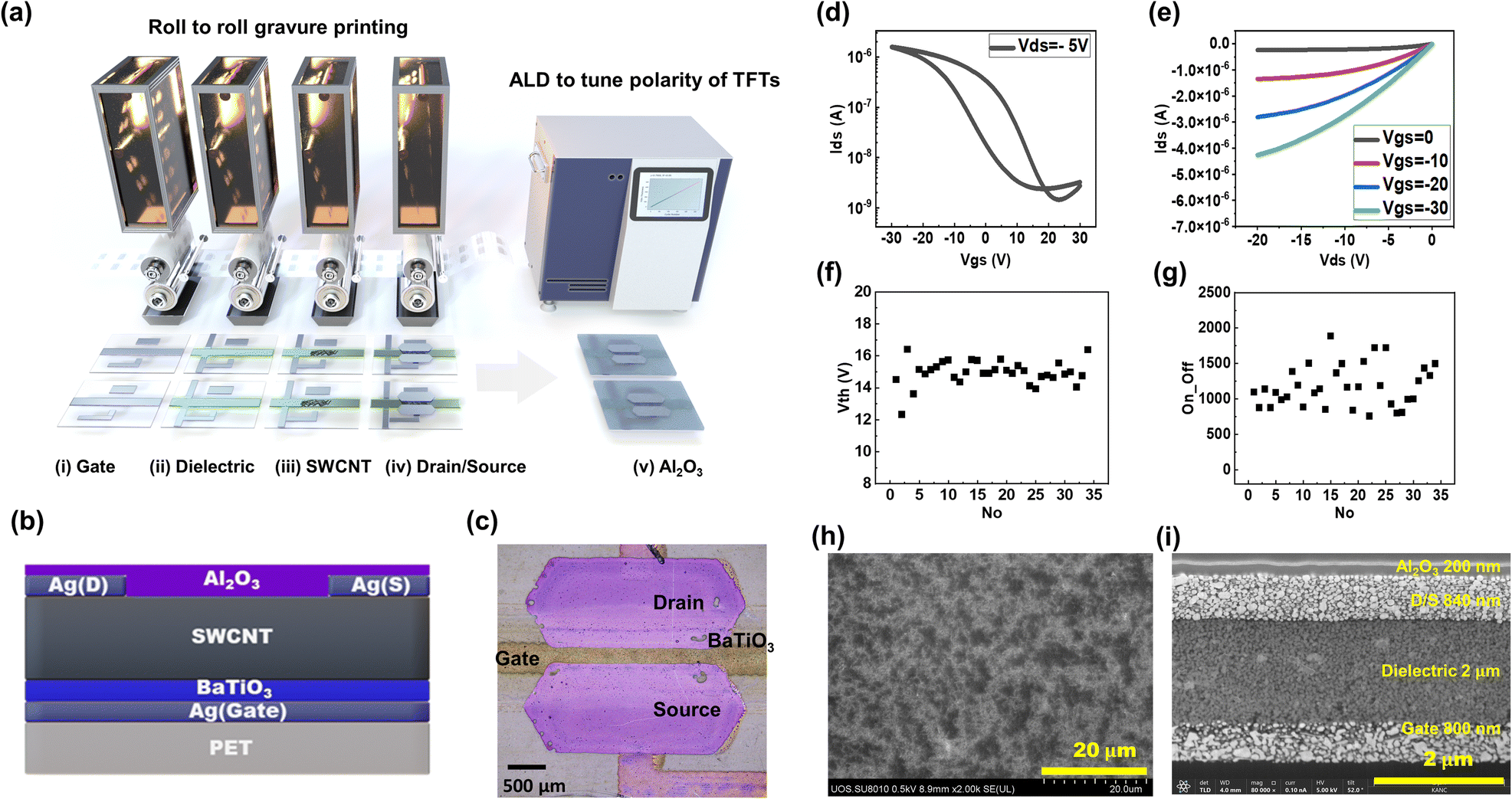 | ||
| Fig. 1 (a) Schematic of the fabrication process for SWCNT-TFTs through R2R printing and ALD process, (b) schematic cross-section view of an R2R printed SWCNT-TFT, (c) optical image of an R2R printed SWCNT-TFT, (d) typical transfer (Vds = −5 V) curve and (e) output curve of R2R printed SWCNT-TFTs, (f) scatter plots of Vth, (g) on–off ratio of 35 devices, (h) SEM image of SWCNT random networks, (i) FIB-SEM cross-sectional image of an R2R printed SWCNT-TFT. | ||
After fabricating SWCNT-TFTs through the R2R gravure printing process, transfer and output characteristics of the printed SWCNT-TFTs were measured under ambient conditions using a semiconductor parameter analyzer (Keithley 4200A-SCS, USA) with a probe station (MST-4000A, MS-TECH, Korea). Thirty-five TFTs with similar electrical properties were chosen from the R2R printed SWCNT-TFTs as the testing samples for depositing the Al2O3 layer via the ALD (step (v) in Fig. 1a). Five devices were put in one group, and all the prepared devices were divided into 7 groups according to different deposition temperatures and thicknesses. To study the effect of deposition temperature, 50 nm thickness of Al2O3 was coated using the ALD method onto the printed SWCNT-TFT samples at temperatures of 150 °C, 140 °C, 130 °C, and 100 °C, respectively. Then, different thicknesses of 50 nm, 100 nm, 150 nm, and 200 nm of Al2O3 were respectively deposited at a deposition temperature of 140 °C. All the devices were carefully attached onto a 6-inch silicon wafer using polyimide (PI) tape and then the silicon wafers with samples were put into the ALD chamber. For the ALD process, trimethylaluminum (TMA) and water were used as precursors. The pulse time of TMA and water precursors was 0.1 s and 0.2 s, respectively, whereas the running time of TMA and water precursors was 30 s and 60 s, respectively. Under this condition, the steady-state growth per cycle is 0.15 nm. The reaction cycles for growing Al2O3 layers with the thickness of 50 nm, 100 nm, 150 nm, and 200 nm were 312, 624, 936, and 1048 respectively.
Characterization and measurements
A device's cross-sectional schematic image and optical microscope image of the printed SWCNT-TFT are shown in Fig. 1b and c respectively. The top view image of a fabricated device was taken using an optical microscope (semiconductor inspection microscope MX51, Olympus, Japan). Unlike silicon-based devices, water and oxygen molecules will permeate the PET film and influence the stability of the devices.29 Therefore, to achieve environmental stability of the printed device, 100 nm thickness of Al2O3 at the temperature of 100 °C was deposited onto the backside of the PET film. Then the Al2O3 was deposited onto the top (upper side) of the devices. The transfer and output characteristics of printed SWCNT-TFTs were measured under ambient conditions (temperature: 25 °C, humidity: 30%) after the Al2O3 deposition. To show the environmental stability, the samples were left under the ambient condition for 48 hours and remeasured. The inverter's voltage transfer curve (VTC) was measured with a semiconductor analyzer (Keithley 4200, Solon, USA) using 4 probes on the probe station (Model 5500, MS-TECH, Korea).Results and discussion
The cross-sectional structure of the fabricated device is shown in Fig. 1b, consisting of the key components of TFTs: gate, BaTiO3 dielectric, SWCNTs, and drain–source layers. As shown in Fig. 1c, the channel length and width of the printed SWCNT-TFT are 170 μm and 1700 μm, respectively. The typical transfer and output characteristics of the pristine printed SWCNT-TFT are respectively shown in Fig. 1d and e. The strong hysteresis behaviour (10–15 V in this work) is caused by trapped surface charges between the SWCNT network structure and the dielectric layer. Indeed, when we modify the surface of the BaTiO3-based dielectric layer to make it hydrophobic, we observed minimal hysteresis in this case. The mobility was calculated from the transconductance, μ = Lgm/WCiVds, where gm and Ci are the transconductance and the gate capacitance per unit, respectively. 10 nF cm−2 was obtained from the capacitance–voltage measurement method to calculate the mobility of our samples. All devices' transfer characteristics are shown in Fig. S1a.† The R2R printed SWCNT-TFT showed an average Vth of 15 ± 1 V (Fig. 1f), mobility of 1.6 ± 0.4 × 10⁻⁴ cm2 V−1 s−1 (Fig. S1b†), transconductance of −3.6 ± 0.4 × 10⁻⁵ s (Fig. S1c†) and on/off ratio of 1200 ± 600 (Fig. 1g) which shows the typical p-type characteristic of printed SWCNT-TFT samples. Since the amount of SWCNTs transferred from the gravure roll to the PET substrate during the R2R gravure printing process significantly impacts the final device characteristics, we confirmed the morphology of the printed SWCNT layer via field emission scanning electron microscopy (FE-SEM), as shown in Fig. 1h. From the obtained FE-SEM image, highly dense network structures of SWCNTs were formed on the BaTiO3 dielectric surface, indicating that they were well connected. In addition, Fig. 1i shows the focused ion beam (FIB) cross-sectional image of the R2R printed SWCNT-TFT with the thicknesses of the gate, dielectrics, and drain/source being 800 nm, 2 μm, and 840 nm, respectively. To better understand carrier type conversion on printed SWCNT-TFTs, we conducted systematic experiments by changing the temperature of the ALD process and the thickness of the Al2O3 layer. First, 50 nm thickness of Al2O3 was deposited onto the R2R-printed SWCNT-TFT samples using the ALD process at different temperatures (100 to 150 °C). The transfer characteristics of SWCNT-TFT samples in Fig. 2a–d reveal the temperature-dependent charge carrier polarity.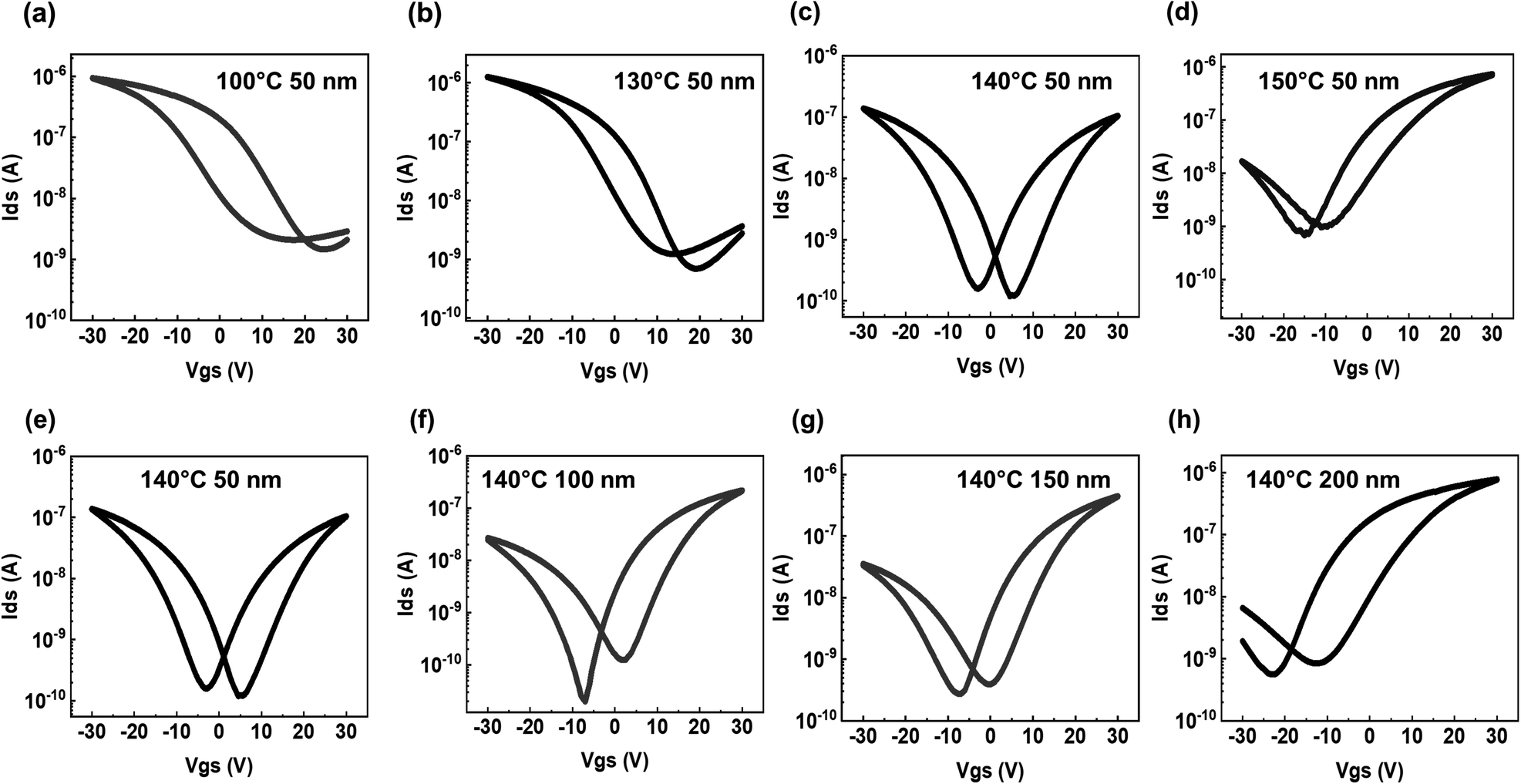 | ||
| Fig. 2 (a)–(d) Transfer characteristics after 50 nm thickness Al2O3 deposition at coating temperatures of 100 °C, 130 °C, 140 °C and 150 °C, respectively. (e)–(h) Transfer characteristics after the Al2O3 deposition at 140 °C with coating thicknesses of 50 nm, 100 nm, 150 nm and 200 nm, respectively. | ||
It is worth noting that, at the temperature of 100 and 130 °C (Fig. 2a and b), the devices show the typical p-type dominant properties, but as the temperature increases to 140 °C (Fig. 2c), the n-type charge carrier of on-current increases while the p-type charge carrier of on-current decreases, showing ambipolar properties interestingly, while at the temperature of 150 °C (Fig. 2d), the devices show n-type charge carrier-dominant properties. All the experiments were repeated (Fig. S2†). On the one hand, as reported previously, this phenomenon is caused by the different amounts of positive fixed charges generated by the deposited Al2O3 layer.30 When the deposition temperature is increased, the H2O, introduced during the ALD process, vaporizes rapidly. Consequently, fewer oxygen atoms are available during the formation of the Al2O3 layer. This leads to a higher deficiency of oxygen atoms within the oxide layer, resulting in the accumulation of more positive charge at a higher deposition temperature. On the other hand, the different temperatures may have different curing effects on the samples. To investigate the curing effect during the deposition process, a sample was cured for 8 hours at the temperature of 100 °C, 130 °C, 140 °C, and 150 °C, respectively. The results show that higher the curing temperature, more the shift of Vth towards 0 V as shown in Fig. S3.† Moreover, Fig. 2e–h show the transfer characteristics of the printed SWCNT-TFT with Al2O3 coating thicknesses of respectively 50 nm, 100 nm, 150 nm, and 200 nm at 140 °C deposition temperature. When the deposition thickness is 50 nm, the device shows ambipolar properties (Fig. 2e). However, when increasing the Al2O3 layer thickness to 100 nm and 150 nm (Fig. 2f and g), the device shows a slightly n-type dominant property. By increasing the thickness to 200 nm, the devices finally become n-type dominant (Fig. 2h). All the experiments were repeated as shown in Fig. S4† and the key electrical parameters of p-type and n-type devices fabricated under different ALD conditions were comparable as shown in Table S1.† Based on the above experiments and our device properties, there might be two possible reasons for the results obtained: the thickness of the Al2O3 layer and the curing time. On the one hand, the differences in the thickness of the Al2O3 layer may affect the density of the fixed positive charge present in the device. A previous report has suggested that thicker Al2O3 layers may result in a higher density of fixed charge.31 As a result, the increased thickness of the Al2O3 layer could induce more electrons in the interface of SiO2/Al2O3, resulting in an electron-richer situation. We can speculate, based on their study, that the thickness difference in the deposited Al2O3 may cause different densities of fixed positive charge which can influence the polarity of printed SWCNT-TFTs. This is supported by the results shown in Fig. 2e, f and S4.† On the other hand, the curing time might be another reason for the conversion from the pristine p-type SWCNT-TFT to the n-type during the ALD process since higher the thickness, more the deposition time required. To prove this, we additionally cured a pristine sample for 24 hours and measured IV characteristics every 8 hours. The results show that the Vth shifts more toward 0 V at a longer curing time as shown in Fig. S5.† Longer the curing time, more the water and oxygen removed from the SWCNT active channel, indicating that fewer holes will be involved as the carriers in the final device properties. Therefore, a similar number of electrons are induced by the deposited Al2O3 while the number of holes is reduced so that the device n-type will finally dominate the final device's property.
Fig. 3 elucidates the mechanism of different charge carrier polarity types of devices. Intrinsic SWCNTs have the ability to conduct electrons and holes. Firstly, R2R gravure printed SWCNT-TFTs show p-type properties due to their exposure to water and oxygen molecules in the ambient air.31 Therefore, the carriers in the SWCNT channel are holes and the Fermi level is close to the valence band (Fig. 3a). The polarity conversion of SWCNT-TFTs is attributed to the deposited Al2O3 which generated a positive fixed charge and could attract electrons in the SWCNT active layer, resulting in the Fermi level shifting towards the conduction band. When the number of electrons and holes in the channel are comparable, the devices show ambipolar properties in which the corresponding Femi level will be located near the middle between the conduction band and valence band (Fig. 3b). However, when the number of electrons is higher than the holes, the device will show n-type charge carrier dominant performance and the Fermi level of this type of device will move towards the conduction band (Fig. 3c). Usually SWCNT-based TFTs are vulnerable to the humidity in the air. Therefore, stable device development is an important step for practical applications of the device. The transfer characteristic curves for the p-type, ambipolar and n-type SWCNT-TFTs are respectively shown in Fig. 4a, b and c for showing the devices' stability under ambient conditions. From the attained transfer characteristic curves, we confirmed that no significant variations were observed in Vth and on/off ratio values between the initial state and the final state after 48 hours under the exposure of moisture and light. This suggests that the deposited Al2O3 layer can prevent water and oxygen from being adsorbed onto its surface. Furthermore, since the stability of the TFT under the bias stress is a critical point for practical applications, the biasing stress effect was further investigated using the printed devices with the deposition of the Al2O3 layer.28 The p-type, ambipolar device, and n-type devices were tested under the biasing voltage of Vgs = 20 V, and the transfer curves were measured every 10 minutes for 30 minutes. As shown in Fig. S6,† the measured transfer curves showed that all devices were stable under biasing stress, indicating the negligible defect density in the active channel. By using ambipolar SWCNT-TFTs, we further constructed inverter logic gates, the schematic of which is shown in Fig. 4d. Here, the noise margin (NM) is another critical parameter affecting the performance of the device consisting of digital logic circuits. Because it quantifies how much external signal perturbation a logic gate circuit can withstand during device operation, the tolerance ability to variations in the signal level is valuable for the integrated logic gates. The high noise margin (NMH) and low noise margin (NML) of the ambipolar TFT based inverter are 2.8 V and 3.4 V respectively as shown in Fig. 4e. In addition, the maximum gain of the inverter is around 4 (Fig. 4f). For inverters built using CMOS devices consisting of symmetric p-type and n-type SWCNT-TFTs (Fig. 4g), the NMH and NML are 4.7 V and 4.6 V, respectively as shown in Fig. 4h, and the maximum gain of the inverter is around 4.2 (Fig. 4i). The detailed transfer curve and output curve of the ambipolar devices and CMOS devices used in the inverter circuit test are shown in Fig. S7a–c.† The characteristics of the ambipolar charge carrier are clearly shown as a diode in Vds–Ids curves for both p-type and n-type measurements when the gate voltage is zero. Regarding the cut-off frequency of the devices, the calculated theoretical cut-off frequency was 202 kHz for the CMOS inverter based on the simple equation fT = gm/2π(CGS + CGD),8 where gm is the transconductance, CGS and CGD are the parasitic capacitances between the drain–source layer and gate layer. However, the observed cut-off frequency of the CMOS inverter was 100 Hz due to the trapped charges at the interface between the printed SWCNT network structure and dielectric layer, causing the huge parasitic capacitance. Based on the results from our previous logic gate circuits such as fully R2R gravure printed 1 bit ring oscillation,16 full adders,7 and 4 bit code generator,17 a voltage gain of 4 is sufficient for operating a simple type of TFT integrated circuits (within 100 TFT integration) with a reasonable degree of functionality. Thus, the ambipolar SWCNT-TFT based printed devices will be easier to develop the practical printed devices than implementing both n-type and p-type SWCNT-TFTs because complementary devices with environmental stability can be efficiently achieved.
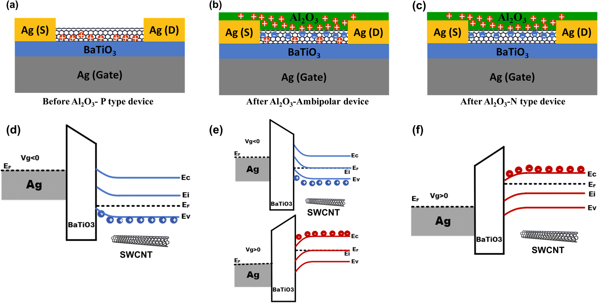 | ||
| Fig. 3 (a) The schematic image of an on-state SWCNT-TFT as printed. (b) Ambipolar device's cross-sectional schematic image of the on-state SWCNT-TFT with the doping mechanism of fixed positive charge generated by the Al2O3 layer. (c) n-Type device's cross-sectional schematic image of the on-state SWCNT-TFT. (d)–(f) The band diagrams respectively for p-type, ambipolar and n-type SWCNT-TFTs. | ||
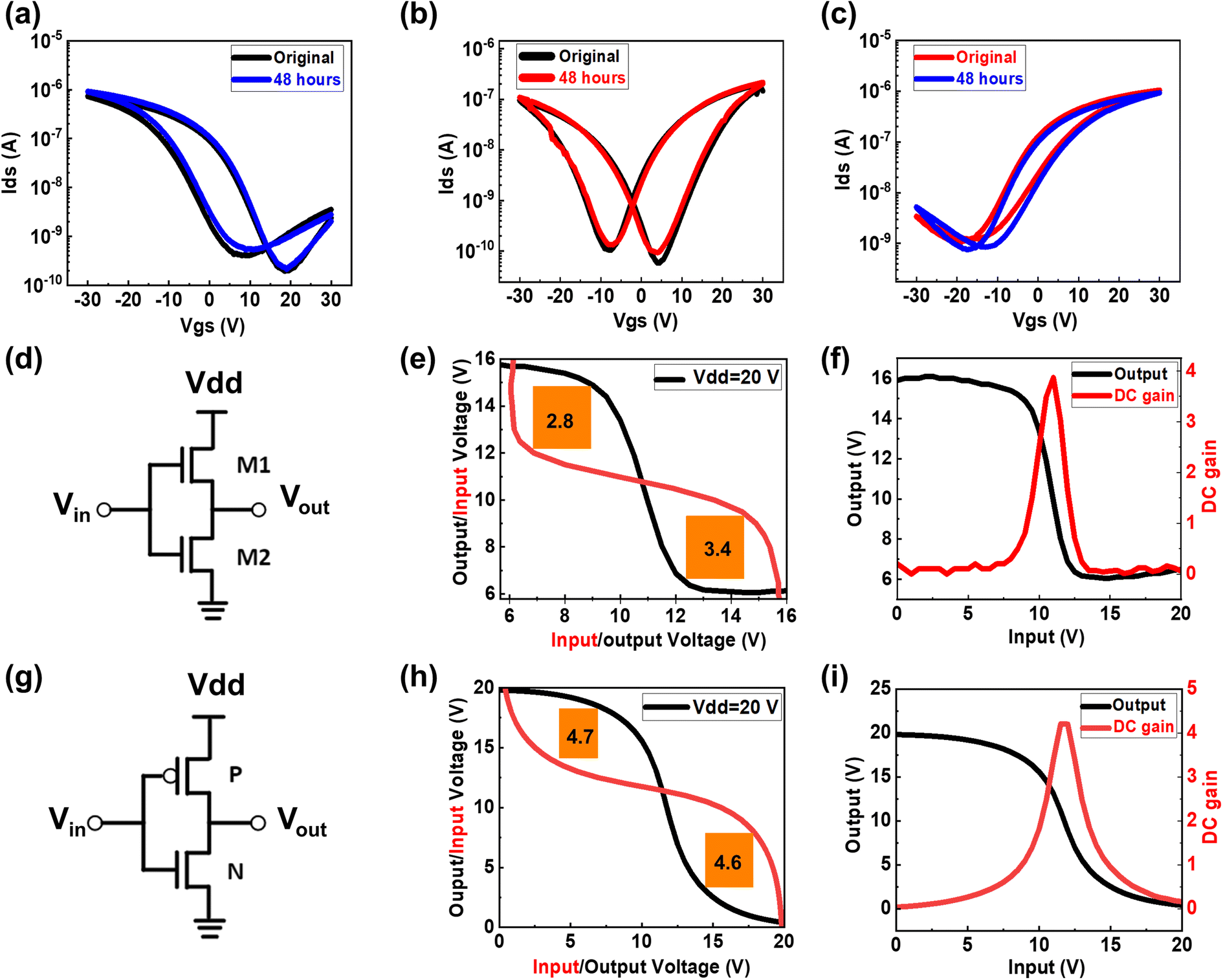 | ||
| Fig. 4 (a) Stability test of Al2O3 coated (a) p-type device, (b) ambipolar device, (c) n-type device. (d) Inverter circuit using two ambipolar devices. (e) Inverter VTC and noise margin at Vdd = −20 V and (f) DC gain of the inverter from ambipolar TFTs. (g) Inverter circuit using CMOS device. (h) Inverter VTC and noise margin at Vdd = −20 V and (i) DC gain of the inverter from the CMOS device. | ||
Conclusions
In conclusion, this study provides a comprehensive understanding of the charge carrier polarity control through the deposited Al2O3 layer via the ALD method on fully R2R printed SWCNT-based flexible TFTs as well as their possibility of being a passivation layer on the printed devices. The Vth shift and charge carrier polarity conversion were successfully demonstrated by adjusting the ALD temperature and alumina (Al2O3) thickness, allowing for the easy fabrication of p-type, ambipolar, and n-type TFTs. Furthermore, all results obtained from all devices, used in this work, were well reproduced with good environmental stability. The study of the inverter based on the ambipolar devices and the CMOS devices shows that both devices can be used to construct inverter circuits. The ambipolar device-based inverter exhibits an NMH of 2.8 V and an NML of 3.4 V, yielding a voltage gain of 3.9, indicating efficient operation of simple types of logic gate circuits within 100 TFT integration. In comparison, the CMOS-based inverter exhibits an NMH of 4.7 V and an NML of 4.6 V, respectively, with a gain of approximately 4.2. These results demonstrate that the ambipolar-based inverter exhibits comparable performance to its CMOS counterpart while eliminating one printing step and improving the devices' environmental stability. In addition, this work serves as a valuable reference for the development of future flexible electronics and provides a systematic explanation of the formation and control of charge carrier polarity in printed SWCNT-based transistors by depositing an Al2O3 layer via the ALD method.Author contributions
W. Z. designed and conducted the experiment. S. S., S. P., J. P., and H. Y. printed the devices. W. Z., S. S., S. P., J. P., H. Y., and B. B. M. analysed the data. W. Z. wrote the manuscript. G. C. and Y. J. supervised the work. All authors have read and agreed to the published version of the manuscript.Conflicts of interest
There are no conflicts to declare.Acknowledgements
This research was supported by grants from the National Research Foundation of Korea, funded by the Korean government (MSIT) (No. 2020R1A5A1019649), and the Technology Innovation Program (20018359, development of design for user biological and environmental information reactive printed electronic chameleon sheet) funded by the Ministry of Trade, Industry & Energy (MOTIE, Korea).Notes and references
- S. J. Han, J. Tang, B. Kumar, A. Falk, D. Farmer, G. Tulevski, K. Jenkins, A. Afzali, S. Oida, J. Ott, J. Hannon and W. Haensch, Nat. Nanotechnol., 2017, 12, 861–865 CrossRef CAS PubMed.
- P. H. Lau, K. Takei, C. Wang, Y. Ju, J. Kim, Z. Yu, T. Takahashi, G. Cho and A. Javey, Nano Lett., 2013, 13, 3864–3869 CrossRef CAS PubMed.
- J. Sun, A. Sapkota, H. Park, P. Wesley, Y. Jung, B. B. Maskey, Y. Kim, Y. Majima, J. Ding, J. Ouyang, C. Guo, J. Lefebvre, Z. Li, P. R. L. Malenfant, A. Javey and G. Cho, Adv. Electron. Mater., 2020, 6, 1901431 CrossRef CAS.
- K. Chen, W. Gao, S. Emaminejad, D. Kiriya, H. Ota, H. Y. Y. Nyein, K. Takei and A. Javey, Adv. Mater., 2016, 28, 4397–4414 CrossRef CAS PubMed.
- P. Feng, W. Xu, Y. Yang, X. Wan, Y. Shi, Q. Wan, J. Zhao and Z. Cui, Adv. Funct. Mater., 2017, 27, 1604447 CrossRef.
- C. Zhu, A. Chortos, Y. Wang, R. Pfattner, T. Lei, A. C. Hinckley, I. Pochorovski, X. Yan, J. W. F. To, J. Y. Oh, J. B. H. Tok, Z. Bao and B. Murmann, Nat. Electron., 2018, 1, 183–190 CrossRef.
- M. Jung, J. Kim, J. Noh, N. Lim, C. Lim, G. Lee, J. Kim, H. Kang, K. Jung, A. D. Leonard, J. M. Tour and G. Cho, IEEE Trans. Electron Devices, 2010, 57, 571–580 CAS.
- H. Koo, W. Lee, Y. Choi, J. Sun, J. Bak, J. Noh, V. Subramanian, Y. Azuma, Y. Majima and G. Cho, Sci. Rep., 2015, 5, 14459 CrossRef CAS PubMed.
- Q. Liu, Y. Wang, A. Kohara, H. Matsumoto, S. Manzhos, K. Feron, S. E. Bottle, J. Bell, T. Michinobu and P. Sonar, Adv. Funct. Mater., 2020, 30, 1907452 CrossRef CAS.
- Z. Li, K. R. Jinkins, D. Cui, M. Chen, Z. Zhao, M. S. Arnold and C. Zhou, Nano Res., 2022, 15, 864–871 CrossRef CAS.
- S. M. Kim, J. H. Jang, K. K. Kim, H. K. Park, J. J. Bae, W. J. Yu, H. Lee, G. Kim, D. D. Loc, U. J. Kim, E. H. Lee, H. J. Shin, J. Y. Choi and Y. H. Lee, J. Am. Chem. Soc., 2009, 131, 327–331 CrossRef CAS PubMed.
- T. J. Ha, K. Chen, S. Chuang, K. M. Yu, D. Kiriya and A. Javey, Nano Lett., 2015, 15, 392–397 CrossRef CAS PubMed.
- H. Wang, P. Wei, Y. Li, J. Han, H. R. Lee, B. D. Naab, N. Liu, C. Wang, E. Adijanto, B. C. K. Tee, S. Morishita, Q. Li, Y. Gao, Y. Cui and Z. Bao, Proc. Natl. Acad. Sci. U. S. A., 2014, 111, 4776–4781 CrossRef CAS PubMed.
- T. Takenobu, T. Takano, M. Shiraishi, Y. Murakami, M. Ata, H. Kataura, Y. Achiba and Y. Iwasa, Nat. Mater., 2003, 2, 683–688 CrossRef CAS PubMed.
- A. Javey, J. Guo, D. B. Farmer, Q. Wang, D. Wang, R. G. Gordon, M. Lundstrom and H. Dai, Nano Lett., 2004, 4, 447–450 CrossRef CAS.
- D. Kim, Y. Jung, J. Sun, C. Yeom, H. Park, D. G. Jung, Y. Ju, K. Chen, A. Javey and G. Cho, Nanoscale, 2016, 8, 19876–19881 RSC.
- H. Park, J. Sun, Y. Jung, J. Park, B. B. Maskey, K. Shrestha, G. R. Koirala, S. Parajuli, S. Shrestha, A. Chung and G. Cho, Adv. Electron. Mater., 2020, 6, 20000770 Search PubMed.
- Y. Ren, X. Yang, L. Zhou, J. Y. Mao, S. T. Han and Y. Zhou, Adv. Funct. Mater., 2019, 29, 1902105 CrossRef.
- B. Kim, M. L. Geier, M. C. Hersam and A. Dodabalapur, ACS Appl. Mater. Interfaces, 2015, 7, 27654–27660 CrossRef CAS PubMed.
- K. Chen, D. Kiriya, M. Hettick, M. Tosun, T. J. Ha, S. R. Madhvapathy, S. Desai, A. Sachid and A. Javey, APL Mater., 2014, 2, 092504 CrossRef.
- S. Liang, Z. Zhang, T. Pei, R. Li, Y. Li and L. Peng, Nano Res., 2013, 6, 535–545 CrossRef CAS.
- R. L. Puurunen, J. Appl. Phys., 2005, 97, 121301 CrossRef.
- R. W. Johnson, A. Hultqvist and S. F. Bent, Mater. Today, 2014, 17, 236–246 CrossRef CAS.
- K. Yoshitsugu, M. Horita, Y. Ishikawa and Y. Uraoka, Phys. Status Solidi C, 2013, 10, 1426–1429 CrossRef CAS.
- P. D. Ye, G. D. Wilk, B. Yang, J. Kwo, S. N. G. Chu, S. Nakahara, H. J. L. Gossmann, J. P. Mannaerts, M. Hong, K. K. Ng and J. Bude, Appl. Phys. Lett., 2003, 83, 180–182 CrossRef CAS.
- M. Mattmann, T. Helbling, L. Durrer, C. Roman, C. Hierold, R. Pohle and M. Fleischer, Appl. Phys. Lett., 2009, 94, 183502 CrossRef.
- E. Carlos, R. Branquinho, A. Kiazadeh, P. Barquinha, R. Martins and E. Fortunato, ACS Appl. Mater. Interfaces, 2016, 8, 31100–31108 CrossRef CAS PubMed.
- F. Shan, A. Liu, H. Zhu, W. Kong, J. Liu, B. Shin, E. Fortunato, R. Martins and G. Liu, J. Mater. Chem. C, 2016, 4, 9438–9444 RSC.
- T. Y. Cho, W. J. Lee, S. J. Lee, J. H. Lee, J. Ryu, S. K. Cho and S. H. Choa, Thin Solid Films, 2018, 660, 101–107 CrossRef CAS.
- J. Zhang, C. Wang, Y. Fu, Y. Che and C. Zhou, ACS Nano, 2011, 5, 3284–3292 CrossRef CAS PubMed.
- D. Hiller, D. Tröger, M. Grube, D. König and T. Mikolajick, J. Phys. D: Appl. Phys., 2021, 54, 275304 CrossRef CAS.
Footnote |
| † Electronic supplementary information (ESI) available. See DOI: https://doi.org/10.1039/d3na00286a |
| This journal is © The Royal Society of Chemistry 2023 |