
 Open Access Article
 This Open Access Article is licensed under a
 Creative Commons Attribution 3.0 Unported Licence
Non-volatile resistive switching mechanism in single-layer MoS2 memristors: insights from ab initio modelling of Au and MoS2 interfaces†
Gabriele
Boschetto
 *a,
Stefania
Carapezzi
a and
Aida
Todri-Sanial
*ab
*a,
Stefania
Carapezzi
a and
Aida
Todri-Sanial
*ab
aLaboratory of Computer Science, Robotics, and Microelectronics, University of Montpellier, CNRS, 161 Rue Ada, 34095 Montpellier, France. E-mail: gabriele.boschetto@lirmm.fr; aida.todri@lirmm.fr
bDepartment of Electrical Engineering, Eindhoven University of Technology, Groene Loper 3, 5612 AE Eindhoven, Netherlands
First published on 21st July 2023
Abstract
Non-volatile memristive devices based on two-dimensional (2D) layered materials provide an attractive alternative to conventional flash memory chips. Single-layer semiconductors, such as monolayer molybdenum disulphide (ML-MoS2), enable the aggressive downscaling of devices towards greater system integration density. The “atomristor”, the most compact device to date, has been shown to undergo a resistive switching between its high-resistance (HRS) and low-resistance (LRS) states of several orders of magnitude. The main hypothesis behind its working mechanism relies on the migration of sulphur vacancies in the proximity of the metal contact during device operation, thus inducing the variation of the Schottky barrier at the metal–semiconductor interface. However, the interface physics is not yet fully understood: other hypotheses were proposed, involving the migration of metal atoms from the electrode. In this work, we aim to elucidate the mechanism of the resistive switching in the atomristor. We carry out density functional theory (DFT) simulations on model Au and ML-MoS2 interfaces with and without the presence of point defects, either vacancies or substitutions. To construct realistic interfaces, we combine DFT with Green's function surface simulations. Our findings reveal that it is not the mere presence of S vacancies but rather the migration of Au atoms from the electrode to MoS2 that modulate the interface barrier. Indeed, Au atoms act as conductive “bridges”, thus facilitating the flow of charge between the two materials.
1 Introduction
Memristors are emerging nanoelectronic devices whose non-volatile properties could enable super-fast and ultra-low power memory chips.1,2 Additionally, memristive devices could also be employed for data encryption3,4 and as synaptic units in the context of brain-inspired (neuromorphic) computing technologies.5–8Memory devices beyond the conventional silicon flash storage, such as resistive random access memories (RRAMs), are typically composed of a core material (i.e., a metal oxide) sandwiched between two metal electrodes.9,10 At the device level, the modulation of the electrical resistance (resistive switching) is achieved by applying external electric stimuli. At the material level, the working mechanism of RRAMs involves the formation and rupture of conductive filaments of either internal ions or ionic vacancies in the oxide channel, mediated by the electric field.11,12 Such a conductive filament is then able to bridge (decouple) the top and bottom electrodes, thus allowing (hindering) electrical charge to flow through the device.
Recently, layered two-dimensional (2D) materials have also been used as novel core materials to develop and fabricate memory devices.7,8,13,14 For instance, non-volatile resistive switching has been observed in devices based on graphene and derivatives,15,16 and on transition metal dichalcogenides (TMDs), such as molybdenum disulphide (MoS2). Similarly to graphene, MoS2 can be thinned down to a single layer, which shows several desirable mechanical, electrical, and optical properties, thus making it the ideal candidate to be used in a wide range of (opto)electronic devices.17–21 Surprisingly, recent work revealed that vertical 2D memristors could also work by employing only one single layer of MoS2 sandwiched between two Au electrodes.22,23 Such a compact device, also known as “atomristor”, has been shown to function at low voltages (≤1 V), thus having the great advantage of being low-power while enabling denser system integration. Moreover, the device retained its properties even after several bending cycles, making it suitable to be used in flexible electronics.
Although other examples of memristors based on single (or few) layer(s) of MoS2 have been reported, the mechanism of the resistive switching in these devices is still not well understood. In general, several factors are thought to come into play, such as the device architecture, the nature of the metal electrodes, whether MoS2 is employed as multi-layer, single-layer or few-layer, its crystallinity, and if the material has been somehow functionalized.24 For instance, the formation of a conductive filament has been hypothesized in a recent memtransistor device based on multilayer MoS2 and with Ag electrodes,25 as well as in another vertical device based on bilayer MoS2 sandwiched between Cu and Au electrodes.26 In both cases, the conductive filament has been attributed to ions migrating from the Ag and Cu active electrodes. Sangwan et al.27 reported a lateral two-terminal device in which the resistive switching was mediated by the presence and orientation of grain boundaries in monolayer (ML) MoS2. Similarly, Wang et al.28 reported a top-gated memory device with polycrystalline MoS2 as the channel, in which the proposed working mechanism involves the migration of sulphur defects (mainly di-vacancies) across the grain boundaries. S vacancies often occur in MoS2 samples obtained by chemical vapour deposition (CVD) and following annealing, and can reach very high densities: typically, on the order of 1013 cm−2.29 With such a high defect density, it is clear that the material is far from being pristine.
It appears that, regardless of the device architecture, S vacancies inevitably occurring in MoS2 are thought to be crucial to trigger the non-volatile resistive switching. Indeed, the main hypothesis behind the working mechanism of the atomristor involves the migration of S vacancies, possibly mediated by the electric field and/or temperature, which diffuse perpendicularly to the electrodes forming filament-like nano-conductive links.22,30,31 Then, the conductive links modulate the Schottky barrier at the electrode interface. Indeed, an impressive switch of several orders of magnitude was observed from the initial high-resistance state (HRS) to the low-resistance state (LRS). Moreover, devices based on ML-MoS2 with multilevel resistive switching have also been reported.30 It is important to point out that such a mechanism is rather unique, and it is different from that occurring in oxide-based devices. Recently, the hypothesis behind the working mechanism of the atomristor has been challenged by experimental studies suggesting that such a significant variation of the electrical resistance is not due to S vacancies alone, but rather to Au atoms migrating from the metal electrode and filling the S vacancies.32,33 This is corroborated by the fact that Au electrodes are known to easily feature adatoms on the surface.34
This paper aims to contribute towards the better understanding of the non-volatile resistive switching mechanism in memristor devices based on ML-MoS2. Given the hypotheses currently at study, both involving migration and diffusion of atoms at the interface between MoS2 and the Au electrode, we carry out atomistic computer simulations within the framework of density functional theory (DFT). Such a simulation approach has been already used to study similar systems and provided invaluable insights into the chemistry and physics of interfaces.35–39 Here, we construct realistic Au/ML-MoS2 model interfaces and we investigate how the presence of defects and Au adatoms at the materials' interface impact the complex physics of memristors. To realistically simulate semi-infinite metal electrodes rather than metal slabs, we employ the Green's function surface model approach. We successfully used this simulation framework in a previous work on defective ML-MoS2 interfaces.39 With our combined DFT-Green's function surface simulations, we aim to provide the necessary theoretical justification to the hypotheses of the non-volatile resistive switching mechanism in single-layer MoS2 memristors.
This paper is organized as follows: in the following section (Simulations details), we provide an overview of our theoretical approach and simulation setup. Then, in Results and discussion, we present the results of our simulations with a discussion in the context of the atomristor. The final section contains the Conclusions.
2 Simulation details
In this work, we focused on defective ML-MoS2 either with point defects or Au adatoms in top contact with the Au(111) electrode. First, we looked at the ideal defect-free interface, in which we initially introduced one single point defect (either one S vacancy or one Au atom filling such vacancy). Then, we systematically increased the concentration of such defects and we varied their position to assess the effect of clustering. From this point onward, unless otherwise specified, we will simply refer to MoS2 to indicate a single-layer structure. Also, we will refer to each Au/MoS2 interface with the name of the defect introduced therein: for instance, VS and AuS correspond to interfaces with one S vacancy and one Au atom filling such a vacancy, respectively. To increase the concentration of defects, we doubled and multiplied by four the number of both S vacancies and Au atoms per unit cell: 2 × VS and 2 × AuS, and 4 × VS and 4 × AuS. We point out that here defects were randomly introduced without any clustering. However, we also investigated the effect of defect clustering, and we considered S di-vacancies either in-plane (VPS2) or axial (VAS2). Equally, we considered axial and in-plane clusters of Au atoms: Au2AS2 and Au2PS2, respectively. Finally, we considered a large 4-atom cluster of S vacancies (VS4).We constructed Au/MoS2 interfaces by matching the crystal lattice of Au(111) to that of MoS2, which led to a small unavoidable mean absolute strain of ∼3% in the Au electrode. The structure of MoS2 was kept free of any strain and with a calculated in-plane lattice constant of 3.16 Å, which matches very well with experimental data.40 It is worth noting that strain on the Au electrode may vary the local registry between Au and MoS2 lattices,36 and consequently may also affect the computed average interface distances. Nevertheless, as we will discuss in the following section, our results compare well with experimental data22 and are well within the range of values found in other computational studies in the literature.36,37,41 To construct such interfaces, we considered a 3 × 3 orthorhombic MoS2 supercell, thus allowing us to keep the concentration of single point defects in the experimental range of ∼1013 cm−2 (equal to a defect density of 2.7%). Such a concentration corresponds to having one single point defect per unit cell, whereas when having two and four the defect density becomes 5.5 and 11%, respectively. The orthorhombic simulation cells of the interfaces had the following dimensions: a = 16.4219 Å, b = 9.4812 Å, and c = 45.5679 Å. A representative interface structure is shown in Fig. 1. Finally, we point out that effects arising from the Moiré pattern between Au(111) and MoS2, as well as the herringbone reconstruction of Au, were not taken into consideration in our simulations.
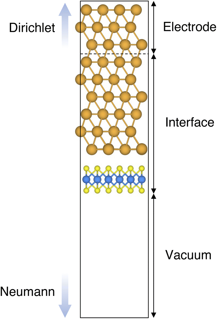 | ||
| Fig. 1 Representative example of the Au/MoS2 interface, modelled with the Green's function surface approach. The system can be divided into three parts: (1) the electrode (to which Dirichlet boundary conditions were applied), (2) the central part, consisting of 6 atomic layers of Au coupled with single-layer MoS2, and (3) the vacuum region, to which Neumann boundary conditions were applied. | ||
Atomistic simulations were carried out in the framework of density functional theory (DFT) with QuantumATK atomic-scale modelling software.42,43 All our spin-polarized calculations were performed in vacuum using the Perdew–Burke–Ernzerhof (PBE) exchange-correlation functional,44 and to model core electrons we used norm-conserving pseudopotentials from the PseudoDojo library.45 The linear combination of atomic orbitals (LCAO) approach was used throughout the work. Upon validation of the simulation settings,39 we chose a density-mesh cut-off of 150 Ry and the QuantumATK-optimized Medium basis set. A k-point mesh defined by a 2 × 3 Monkhorst–Pack (MP) grid46 was used to carry out geometry optimizations, which we increased up to 8 × 12 when computing device density of states (DOS). Geometry optimizations were converged with a maximum allowed atomic force threshold of 0.05 eV Å−1. To take into account long-range dispersion interactions, all the simulations were carried out by including the Grimme's D2 dispersion correction.47 Au/MoS2 interfaces were modelled via the Green's function surface approach as implemented in QuantumATK, which allowed us to construct semi-infinite (fully periodic in one direction) Au surfaces rather than rely on metal slabs.48 To carry out such simulations, we considered six atomic layers of Au coupled with MoS2, to which we imposed Dirichlet boundary conditions in the direction of the bulk Au electrode and Neumann boundary conditions in the vacuum direction (see Fig. 1). A total of 138 k-points along the direction of the Au electrode were chosen.
Adhesion energies (Ead) of MoS2 (pristine and defective) on the Au electrode were computed as:
| Ead = EAu/MoS2 − (EMoS2 + EAu) | (1) |
3 Results and discussion
Here, we discuss on the quality of Au/MoS2 contacts by looking at their optimized interface structures, by computing figures of merit to assess their stability, and by predicting their tunnelling probabilities of electrons.3.1 Structures and stability of defective interfaces
In this part of the work, we focus on the stability of defective interfaces with respect to the pristine case by looking ad their DFT-optimized geometries and by computing adhesion energies (per surface Au atom). The atomic structure of selected interfaces are shown in Fig. 2, whereas average interface distances (dAu–MoS2) and adhesion energies are presented in Table 1. For each interface, we decomposed the total Ead into its dispersion (Edispad) and electrostatic (Eelecad) contributions.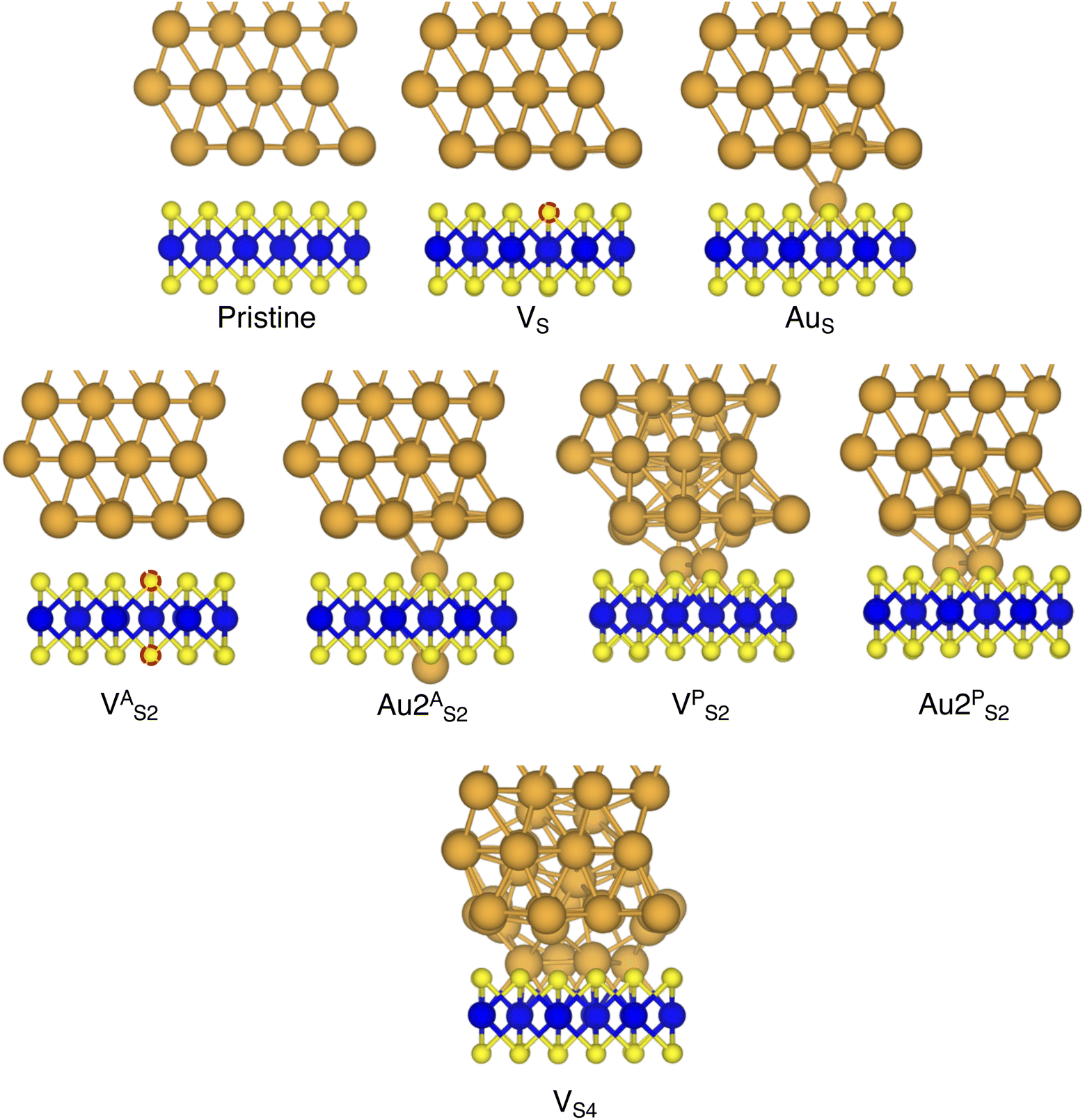 | ||
| Fig. 2 Optimized geometries with DFT of selected Au/MoS2 interfaces considered in this work. The pictures were taken in the vicinity of the contact area between the two materials. Interfaces VPS2 and VS4 refer to MoS2 with clusters of two and four S vacancies, although following geometry optimization such clusters were fully filled by Au atoms migrating from the above electrode. | ||
| Interface | d Au–MoS2 (Å) | E ad (eV) | E dispad (eV) | E elecad (eV) |
|---|---|---|---|---|
| Pristine39 | 2.71 | −0.34 | −0.39 | +0.05 |
| VS39 | 2.73 | −0.34 | −0.38 | +0.04 |
| AuS | 2.72 | −0.42 | −0.41 | −0.01 |
| 2 × VS39 | 2.70 | −0.34 | −0.37 | +0.03 |
| 4 × VS39 | 2.67 | −0.34 | −0.36 | +0.02 |
| 2 × AuS | 2.74 | −0.49 | −0.43 | −0.06 |
| 4 × AuS | 2.76 | −0.64 | −0.45 | −0.19 |
| VAS2 (ref. 39) | 2.70 | −0.34 | −0.38 | +0.04 |
| VPS2 | — | −0.51 | −0.40 | −0.11 |
| VS4 | — | −0.68 | −0.41 | −0.27 |
| Au2AS2 | 2.72 | −0.42 | −0.41 | +0.01 |
| Au2PS2 | 2.74 | −0.49 | −0.42 | −0.07 |
By looking at the optimized structure of the ideal defect-free interface, it is evident that there exist no chemical bonds between Au and MoS2: with an average dAu–MoS2 of 2.71 Å, the interaction between Au and defect-free MoS2 is mainly driven by dispersion forces (van der Waals gap). This is corroborated by the Ead of the interface, whose major contribution is given by Edispad with a small electrostatic repulsion. The weak interaction between Au and pristine MoS2 has been widely reported in the literature with theoretical simulations36,41,50 and in our previous work.39 However, experimental CVD-MoS2 samples are far from being pristine, and are mainly characterized by the presence of S vacancies. Our simulations show that such a defect at 2.7% density (approximately as in experimental samples29) does not significantly change the weak Au/MoS2 interaction: dAu–MoS2 (2.73 Å) is comparable with that of the pristine interface, and the adhesion energy is still mainly given by weak dispersion forces. It is worth noting that the vdW gap between Au and CVD-MoS2 is also observed experimentally by looking at atomic resolution TEM images.22,51 Moreover, the size of the vdW gap that can be extracted by TEM images compares reasonably well with our computed value, thus further confirming our results. We then filled the S vacancy by introducing one Au atom and we optimized the full interface. By doing so, we considered the extra Au atom to be originally adsorbed on the metal electrode (extra adatom). Our simulations revealed that the bond length between Au and the Mo atoms of MoS2 is much longer than that between S and Mo (see Fig. 3) in the same material. We found the Au–Mo bond length to be 2.81 Å, which is 0.40 Å longer than the typical Mo–S bond length (2.41 Å). Thus, the Au atom sticks out of the basal plane of MoS2, allowing it to simultaneously bond also with the Au electrode. We found the bond lengths between the extra Au atom in MoS2 and the four closest Au atoms of the metal electrode to range between 3.15 and 2.70 Å (see Fig. 3). Interestingly, we point out that the Au–Au bond length in the electrode is 2.73 Å. The formation of a chemical bond between the extra Au atom and the metal electrode is further corroborated by the electron localization function (ELF), which we plotted in Fig. 3, and by the electron density difference (EDD) maps in Fig. 4. From the ELF plot, it is evident that there is a non-zero probability to locate electrons between the extra Au and the atoms of the electrode, whereas no direct chemical bonds are observed between S atoms and the metal electrode. Furthermore, EDD maps show a significant charge redistribution on the extra Au atom, whereas with pristine MoS2 and VS only a limited charge redistribution is found at the materials' interface. Overall, the average dAu–MoS2 in AuS is comparable to that of the defect-free interface, although we point out that we observed a small rearrangement of the Au atoms of the electrode due to the presence of the extra Au atom above the basal plane of MoS2. Finally, the stronger interaction between MoS2 and the metal electrode is also corroborated by the stronger Ead, in which, in addition to the dispersion contribution, we also found a small electrostatic attraction (see Table 1). In conclusion, our simulations suggest that the extra Au atom that fills the S vacancy is able to act as a physical “bridge” between MoS2 and the metal electrode.
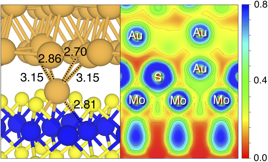 | ||
| Fig. 3 Optimized geometry of the AuS interface (left image), in the proximity of the contact area. Relevant Au–Mo and Au–Au bond lengths (in angstrom) are shown. Contour plot of the ELF for the AuS interface (right image) in the proximity of the contact area. The color scheme is RGB, and red corresponds to ELF = 0, whereas blue to ELF = 0.8. | ||
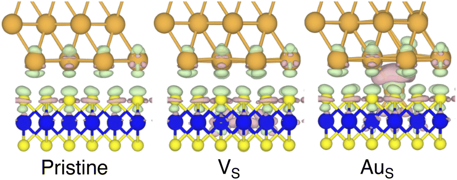 | ||
| Fig. 4 Electron density difference (EDD) maps of the pristine, VS, and AuS interfaces in the vicinity of the contact area. Green colour corresponds to electron loss, whereas mauve colour to electron enrichment. The isovalue was set to 0.002 eV Å−3. | ||
Then, we increased the concentration of both S vacancies and Au substitutions in MoS2. To do so, we doubled and multiplied by four the number of these defects in the simulation cell, resulting in a defect density of 5.5 and 11%, respectively. To avoid artificial clustering, we introduced defects randomly. Once again, we found a limited interaction between the metal electrode and MoS2 in both 2 × VS and 4 × VS, suggesting that even at much higher concentrations the interface is characterized by a vdW gap. However, we observed a small (but negligible) decrease of dAu–MoS2, from 2.71 Å (pristine interface) to 2.70 Å and 2.67 Å for 2 × VS and 4 × VS, respectively. The weak interaction is also confirmed by Ead, whose value did not vary with respect to the pristine interface even at 11% density of S vacancies. On the contrary, we found that increasing the concentration of substitutional Au atoms leads to a significant increase in the electrode/MoS2 interaction. This is evident by looking at Ead, which increased from −0.42 eV in AuS to −0.49 eV and −0.64 eV in 2 × AuS and 4 × AuS, respectively. Interestingly, we point out that the Ead in 4 × AuS is essentially two times that in 4 × VS. It is also worth noting that the electrostatic attraction contribution in the adhesion energy increases with respect to the concentration of substitutional Au atoms: at the highest Au defect density, it accounts for roughly 30% of the total Ead. This is further proof of the capability of substitutional Au atoms to couple the metal electrode to MoS2 by forming strong chemical bonds simultaneously with both materials. On the contrary, increasing the concentration of S vacancies does not lead to any significant change. Finally, we found a slight increase of dAu–MoS2 up to 2.76 Å at 11% defect density, which is the result of the atomic rearrangement of the surface Au atoms of the electrode when in contact with the substitutional Au atoms in MoS2.
Finally, we considered small and bigger clusters of defects at the Au/MoS2 interface. This is relevant, as S vacancies in MoS2 have been shown to be rather mobile and thus possibly prone to clustering.52–54 Our computed formation energies of defects also corroborate this (see Table S1 in the ESI†). Au atoms migrating from the electrodes may then fill such clusters, forming in turn Au clusters. Here, we focused on S di-vacancy and substitutional Au either in or out of plane MoS2. Moreover, we also considered a large 4-atom cluster of S vacancies. We found that both VAS2 and Au2AS2 interfaces (i.e., with axial defects) are characterized by the same Ead and roughly the same dAu–MoS2 of their corresponding VS and AuS interfaces. This is justified by effectively having only one defect in MoS2 in contact with the Au electrode, whereas the other is on the opposite side of the material in contact with the vacuum. Therefore, these results suggest that defects on the opposite (bottom) surface of the material have very little or no effect on the structure and the interface energetics of the (top) Au/MoS2 contact. In the presence of both top and bottom contacts, each vacancy will then play the same role with the Au electrode in proximity. On the contrary, when we coupled MoS2 with in-plane clusters of two and four S vacancies with the metal electrode, we observed the strong tendency of the Au atoms at the bottom layer of the electrode to migrate and fill such clusters, in accordance with previous studies in the literature.35 Remarkably, we found that even a small cluster of two S vacancies was enough to cause the Au electrode to partially collapse on MoS2. We point out that this was not the case when we randomly introduced the same number of S vacancies per unit cell without any clustering, meaning that their relative position can dramatically change the interaction between materials at their interface. Interestingly, when looking at the structures of both VPS2 and VS4 we observed the tendency of the collapsed Au atoms to reorganize and form small metal clusters, rather than just sit in the position of S vacancies. Indeed, from Fig. 5 one can observe that the Au–Au bond lengths are in every case smaller than the typical distance of 3.16 Å of S vacancies. As expected, the computed Ead of both interfaces are very high, confirming the strong interaction between MoS2 and the collapsed Au electrode. The final interface considered in this work was Au2PS2, which essentially corresponds to the situation in which two Au atoms adsorbed on the metal electrode migrate to fill a small cluster of two S vacancies (or two substitutional Au atoms migrate on the MoS2 surface to eventually coalesce). For this interface, we found the same values of both dAu–MoS2 and Ead as in 2 × AuS, suggesting that when no collapse of the electrode occurs the relative position of substitutional Au atoms has little influence on the quality of the contact.
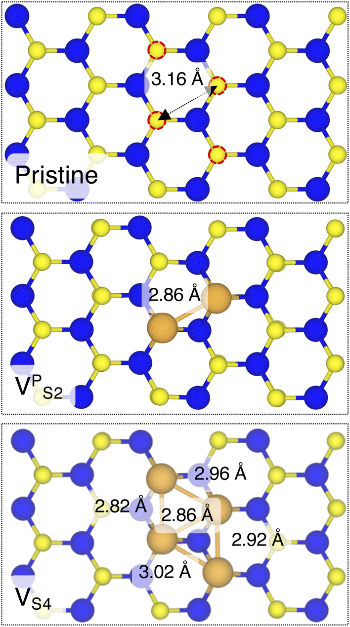 | ||
| Fig. 5 Top view of pristine, VPS2, and VS4 interfaces, where the Au electrode was removed for clarity. | ||
3.2 Tunnelling probabilities of defective interfaces
So far, we have only looked at the structural properties of interfaces. In this part of the work, for each interface considered in this study, we computed electron tunnelling barriers and probabilities as an estimate of the charge transport across the Au/MoS2 contact. In device contacts where no chemical bonding occurs between the metal and the semiconductor (as in the structures here considered), a tunnelling barrier is always present.50,55 Its magnitude correlates with the contact resistance: a high tunnelling barrier implies a low probability of electrons to cross the metal–semiconductor interface, and thus an expected high contact resistance. To extract the tunnelling probability, we computed the plane averaged effective potential (Veff) across the interface of every Au/MoS2 contact considered in this work, and we projected it in the direction of the interface between the two materials. This quantity is shown in Fig. 6, which refers to the defect-free situation. The barrier height (ΦTB) is essentially the difference between Veff in the Au electrode and at the interface, as highlighted in the figure. ΔL is instead the barrier width. Although both ΦTB and ΔL can provide a first estimate of how intimate (or poor) the metal–semiconductor contact is, the tunnelling probability (T) provides a better quantitative figure of merit. We computed T by integrating Veff between the limits defined by the barrier width (see Fig. 6):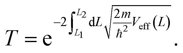 | (2) |
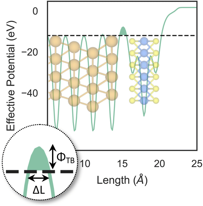 | ||
| Fig. 6 Effective potential across the interface of the pristine Au/MoS2 structure. The potential was projected in the direction of the interface. Highlighted in the figure are the tunnelling barrier height (ΦTB) and the barrier width (ΔL). | ||
In the above equation, m and ℏ are the electron effective mass and the reduced Planck's constant, respectively.
The computed barrier widths, heights, and the tunnelling probabilities are summarized in Table 2. As we found in our previous work,39 the tunnelling probability in the defect-free interface is close to 40%. This quantity slightly decreases to 38–39% when introducing S vacancies, suggesting the worsening of the contact quality regardless of the defect concentration. Thus, with a lower value of T such defective interfaces are expected to have an even larger contact resistance compared to the pristine interface. On the other hand, Au substitution was found to increase the tunnelling probability of the interface from 44.9% at the lowest concentration (AuS) up to 71.1% at the highest concentration (4 × AuS). Interestingly, T correlates very well with the Au concentration, whereas we observed no correlation when increasing the concentration of S vacancies in MoS2, at least until the maximum defect density here considered (11%). This suggests that S vacancies do not play any significant active role in the coupling between MoS2 and the electrode. On the contrary, the effect of Au concentration in the tunnelling probability is evident, suggesting a constant improvement of the electron injection rate as more conductive “bridges” are generated at the interface. It is also worth noting that the value of T in 2 × AuS and Au2PS2 is comparable (50.5 and 50.9%, respectively), whereas in VPS2 (i.e., when the electrode collapses) T is 54%. These results suggest that, at equal concentrations of substitutional Au atoms: (i) when the extra Au atoms derive from the Au electrode as adsorbed adatoms, the effect of clustering on the electron injection rate is negligible; (ii) when the extra Au atoms derive from the collapsed electrode, the tunnelling probability is higher. This can also be observed when comparing values of T in 4 × AuS against VS4 (i.e., when the electron collapses): 71.1 and 89.6%, respectively. We believe this effect to be due to the significant atomic distortion of the Au electrode upon its collapse on MoS2, which effectively leads to a shorter average interface distance than that observed when randomly distributing substitutional Au atoms at the materials' interface.
| Interface | ΔL (Å) | Φ TB (eV) | T (%) |
|---|---|---|---|
| Pristine39 | 0.851 | 3.54 | 39.7 |
| VS39 | 0.875 | 3.55 | 38.5 |
| AuS | 0.773 | 2.94 | 44.9 |
| 2 × VS39 | 0.891 | 3.60 | 38.3 |
| 4 × VS39 | 0.891 | 3.58 | 38.2 |
| 2 × AuS | 0.641 | 2.40 | 50.5 |
| 4 × AuS | 0.333 | 0.85 | 71.1 |
| VAS2 (ref. 39) | 0.868 | 3.64 | 39.0 |
| VPS2 | 0.560 | 1.97 | 54.0 |
| VS4 | 0.110 | 0.23 | 89.6 |
| Au2AS2 | 0.729 | 2.90 | 45.0 |
| Au2PS2 | 0.627 | 2.33 | 50.9 |
3.3 Electronic structure of MoS2 in defective interfaces
To investigate how the electronic properties of MoS2 within the contact change due to the presence of defects, we computed the density of states (DOS) of selected interfaces, projected onto the Mo-4d and S-3p orbitals of MoS2. The projected DOS (PDOS) plots are shown in Fig. 7.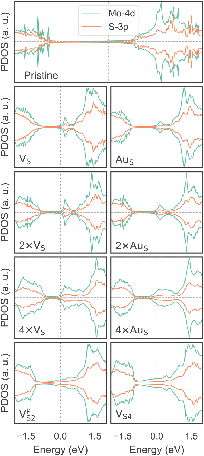 | ||
| Fig. 7 Density of states of selected interfaces, projected onto the Mo-4d and S-3p orbitals of MoS2. The plots, which result from the Green's function surface simulations, are centered around the Fermi level of each system (vertical dotted line). | ||
As expected, the pristine MoS2 retains its band gap also in the presence of the Au electrode. We computed its value to be ∼1.75 eV, in excellent agreement with experimental data.20 We note, however, the shift of the Fermi level towards the conduction band, indicating the n-type doping effect of the Au electrode. In general, the presence of S vacancies does not change the current picture: the material retains its semiconducting properties, although we observed the formation of intra-gap states in the proximity of the conduction band. At a defect density of 11% (4 × VS), several intra-gap states merging with the conduction band of MoS2 are observed. Nevertheless, the Fermi level of the system is still found within the material's band gap, although being very close to the new conduction band edge.
The presence of substitutional Au atoms also leads to intra-gap states close to the conduction band edge of MoS2. Interestingly, at the high defect density of 11% (4 × AuS) we found such intra-gap states to cross the Fermi level of MoS2, suggesting the metallization of the material. We point out that this is consistent with our previous results on adhesion energies and tunnelling probabilities, which both pointed towards the enhanced interaction between the electrode and MoS2, and thus to an intimate device contact. We observed the metallization of MoS2 also in both VPS2 and VS4, where our simulations showed the collapse of the Au electrode. Notably, the PDOS of VS4 shows the complete vanishing of the material's band gap, which indeed correlates with the highest value of T (89.6%) computed in this work, among all the interfaces considered.
Overall, our results show that substitutional Au atoms at higher concentrations cause MoS2 to switch from a semiconductor to a metal, and this is expected to significantly change the resistance at the device contact (see Table 2). Also, we could confirm that the conduction in the LRS of the atomristor is indeed metallic, as it was previously argued by experimental studies.22,30
3.4 Mechanism of the resistive switching
Based on the results presented so far, we propose the following steps behind the resistive switching in vertical Au/MoS2/Au memristors:1. CVD-MoS2 with its typical S vacancy density (∼1013 cm−2) is in contact with the Au electrode. This is well represented by the interface VS, as shown in Fig. 8.
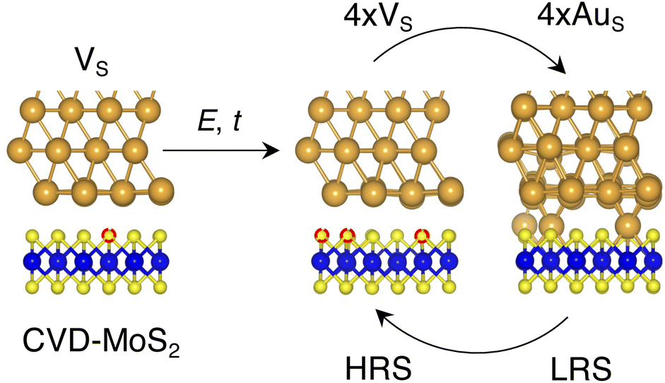 | ||
| Fig. 8 Illustration of the proposed resistive switching mechanism and the possible Au/MoS2 interfaces involved. Here, we propose the electric field (E) and/or temperature (t) as key quantities to generate extra S vacancies and to force the migration of Au atoms from (to) the metal electrode. | ||
2. As the device is switched on for the first time, extra S vacancies are generated due to either the presence of the electric field or the increase in the local temperature. This situation corresponds to the HRS. Among the interface structures considered in this study, 4 × VS (T = 38.2%) would correspond to the best case scenario in which the highest density of S vacancies is obtained (see Fig. 8).
3. Extra Au atoms migrate from the electrode to MoS2, where they are able to fill the S vacancies. The Au migration may be due to both the electric field and the Joule heating caused by it. The computed charge distribution of selected interfaces (see Fig. S1 in the ESI†) shows that extra Au atoms assume a positive partial charge, thus confirming the susceptibility of such atoms to the electric field. The substitutional Au atoms in MoS2 act as conductive “bridges”, thus allowing electrons to easily flow across the contact. In this situation, MoS2 becomes metallic and this corresponds to the LRS. Assuming the highest density of S vacancies, the LRS is best represented by the interface 4 × AuS (T = 71.1%), as can be seen in Fig. 8.
4. To reset the device, an opposite electric field may be applied, forcing substitutional Au atoms to migrate back to the metal electrode, thus restoring the HRS.
In this picture, we note that extra Au atoms may derive either from adatoms adsorbed on the Au(111) surface or directly from the electrode upon its collapse on MoS2, provided a (small or large) cluster of S vacancies is present on the material's surface. As previously discussed, clusters of vacancies may form due to the mobility of S vacancies in MoS2. This process is usually aided by the presence of the electric field or the increase in the local temperature due to self-heating in the device. Assuming the collapse of the Au electrode, resetting the device may not always be possible: very high temperatures and a high electric field may both be needed. This suggests that the electrode collapse could lead to a failure mechanism in which the device is stuck in the LRS. The formation of clusters of S vacancies may then be detrimental.
4 Conclusions
To conclude, by means of a computational modelling approach which combines DFT and Green's function surface simulations, we unravelled the physics of the resistive switching in vertical memristors based on single-layer MoS2 and Au electrodes. To achieve this, we carried out several ab initio simulations of pristine and defective Au/MoS2 interfaces with either S vacancies or substitutional Au atoms. Also, we varied the concentration of such defects and we considered the formation of defect clusters. To shed light onto the memristive mechanism, we explored the impact of defects on the structural and electronic properties of interfaces, and on their tunnelling probabilities.Our simulations revealed that the switch between HRS and LRS in MoS2-based memristors is not due to the mere presence of S vacancies in CVD-MoS2, but rather to the migration of Au atoms from the metal electrode to MoS2. When migrating, these extra Au atoms occupy the position of the S vacancies and are able to act not only as physical but also as conductive “bridges” between the two materials, enhancing the transfer of electrons from the electrode to MoS2. Based on such findings, we believe that the HRS corresponds to the situation in which only S vacancies are present in the material, whereas the LRS is achieved when a sufficient number of Au atoms have migrated and filled the S vacancies in MoS2, which then becomes metallic. This hypothesis is corroborated by the interface geometries, clearly showing the extra Au atoms to simultaneously bind with MoS2 and the Au electrode. Also, the computed tunnelling probabilities of electrons are significantly higher only in the presence of substitutional Au atoms in MoS2. On the contrary, when only S vacancies are present in the material the tunnelling probability is low and comparable to that of the defect-free interface. The PDOS plots of the interfaces confirm this, and show the metallization of MoS2 at higher concentrations of substitutional Au atoms. We also found that extra Au atoms may derive either from adatoms adsorbed on the Au surface, or directly from the electrode upon its collapse on MoS2. The electrode collapse was observed only if clusters of S vacancies are present in the material and could lead to a failure mechanism in which the device is stuck in the LRS.
We point out that the results presented in this work not only support the experimental findings in the literature, but also provide a theoretical understanding of the resistive switching mechanism in vertical Au/MoS2/Au memristors. We hope our work will contribute towards the optimal design and development of 2D memristors.
Author contributions
Gabriele Boschetto: conceptualization, methodology, validation, formal analysis, investigation, data curation, writing – original draft, writing – review & editing, visualization; Stefania Carapezzi: conceptualization, writing – review & editing; Aida Todri-Sanial: conceptualization, writing – review & editing, supervision, project administration, funding acquisition.Conflicts of interest
There are no conflicts to declare.Acknowledgements
The authors acknowledge funding from the European Union's Horizon 2020 research and innovation programme, EU H2020 NeurONN project (https://www.neuronn.eu), grant agreement No. 871501. This work was granted access to the HPC/AI resources of IDRIS (Institut du Développement et des Ressources en Informatique Scientifique) under the allocation 2021-A0110811060 made by GENCI (Grand Équipement National de Calcul Intensif).Notes and references
- K. M. Kim, J. Zhang, C. Graves, J. J. Yang, B. J. Choi, C. S. Hwang, Z. Li and R. S. Williams, Nano Lett., 2016, 16, 6724–6732 CrossRef CAS PubMed.
- M. Lanza, A. Sebastian, W. D. Lu, M. Le Gallo, M.-F. Chang, D. Akinwande, F. M. Puglisi, H. N. Alshareef, M. Liu and J. B. Roldan, Science, 2022, 376, eabj9979 CrossRef CAS PubMed.
- S. Balatti, S. Ambrogio, R. Carboni, V. Milo, Z. Wang, A. Calderoni, N. Ramaswamy and D. Ielmini, IEEE Trans. Electron Devices, 2016, 63, 2029–2035 Search PubMed.
- C. Wen, X. Li, T. Zanotti, F. M. Puglisi, Y. Shi, F. Saiz, A. Antidormi, S. Roche, W. Zheng, X. Liang, J. Hu, S. Duhm, J. B. Roldan, T. Wu, V. Chen, E. Pop, B. Garrido, K. Zhu, F. Hui and M. Lanza, Adv. Mater., 2021, 33, 2100185 CrossRef CAS PubMed.
- D. Ielmini and H.-S. P. Wong, Nat. Electron., 2018, 1, 333–343 CrossRef.
- D. Li, B. Wu, X. Zhu, J. Wang, B. Ryu, W. D. Lu, W. Lu and X. Liang, ACS Nano, 2018, 12, 9240–9252 CrossRef CAS PubMed.
- W. Huh, D. Lee and C.-H. Lee, Adv. Mater., 2020, 32, 2002092 CrossRef CAS PubMed.
- F. Xue, C. Zhang, Y. Ma, Y. Wen, X. He, B. Yu and X. Zhang, Adv. Mater., 2022, 34, 2201880 CrossRef CAS PubMed.
- A. Sawa, Mater. Today, 2008, 11, 28–36 CrossRef CAS.
- H. Akinaga and H. Shima, Proc. IEEE, 2010, 98, 2237–2251 CAS.
- R. Waser and M. Aono, Nat. Mater., 2007, 6, 833–840 CrossRef CAS PubMed.
- J. J. Yang, M. D. Pickett, X. Li, D. A. A. Ohlberg, D. R. Stewart and R. S. Williams, Nat. Nanotechnol., 2008, 3, 429–433 CrossRef CAS PubMed.
- X. Yan, Q. Zhao, A. P. Chen, J. Zhao, Z. Zhou, J. Wang, H. Wang, L. Zhang, X. Li, Z. Xiao, K. Wang, C. Qin, G. Wang, Y. Pei, H. Li, D. Ren, J. Chen and Q. Liu, Small, 2019, 15, 1901423 CrossRef PubMed.
- H. Duan, S. Cheng, L. Qin, X. Zhang, B. Xie, Y. Zhang and W. Jie, J. Phys. Chem. Lett., 2022, 13, 7130–7138 CrossRef CAS PubMed.
- C. L. He, F. Zhuge, X. F. Zhou, M. Li, G. C. Zhou, Y. W. Liu, J. Z. Wang, B. Chen, W. J. Su, Z. P. Liu, Y. H. Wu, P. Cui and R.-W. Li, Appl. Phys. Lett., 2009, 95, 232101 CrossRef.
- A. Rani and D. H. Kim, J. Mater. Chem. C, 2016, 4, 11007–11031 RSC.
- D. Akinwande, C. J. Brennan, J. S. Bunch, P. Egberts, J. R. Felts, H. Gao, R. Huang, J.-S. Kim, T. Li, Y. Li, K. M. Liechti, N. Lu, H. S. Park, E. J. Reed, P. Wang, B. I. Yakobson, T. Zhang, Y.-W. Zhang, Y. Zhou and Y. Zhu, Extreme Mech. Lett., 2017, 13, 42–77 CrossRef.
- B. Radisavljevic, A. Radenovic, J. Brivio, V. Giacometti and A. Kis, Nat. Nanotechnol., 2011, 6, 147–150 CrossRef CAS PubMed.
- S. Ahmed and J. Yi, Nano-Micro Lett., 2017, 9, 50 CrossRef PubMed.
- K. F. Mak, C. Lee, J. Hone, J. Shan and T. F. Heinz, Phys. Rev. Lett., 2010, 105, 136805 CrossRef PubMed.
- C. Yim, M. O'Brien, N. McEvoy, S. Winters, I. Mirza, J. G. Lunney and G. S. Duesberg, Appl. Phys. Lett., 2014, 104, 103114 CrossRef.
- R. Ge, X. Wu, M. Kim, J. Shi, S. Sonde, L. Tao, Y. Zhang, J. C. Lee and D. Akinwande, Nano Lett., 2018, 18, 434–441 CrossRef CAS PubMed.
- M. Kim, R. Ge, X. Wu, X. Lan, J. Tice, J. C. Le and D. Akinwande, Nat. Commun., 2018, 9, 2524 CrossRef PubMed.
- Y. Qiao, T. Hirtz, F. Wu, G. Deng, X. Li, Y. Zhi, H. Tian, Y. Yang and T.-L. Ren, ACS Appl. Electron. Mater., 2020, 2, 346–370 CrossRef CAS.
- M. Farronato, M. Malegari, S. Ricci, S. Hashemkhani, A. Bricalli and D. Ielmini, Adv. Electron. Mater., 2022, 8, 2101161 CrossRef CAS.
- R. Xu, H. Jang, M.-H. Lee, D. Amanov, Y. Cho, H. Kim, S. Park, H.-J. Shin and D. Ham, Nano Lett., 2019, 19, 2411–2417 CrossRef CAS PubMed.
- V. K. Sangwan, D. Jariwala, I. S. Kim, K.-S. Chen, T. J. Marks, L. J. Lauhon and M. C. Hersam, Nat. Nanotechnol., 2015, 10, 403–406 CrossRef CAS PubMed.
- L. Wang, W. Liao, S. W. Wong, Z. G. Yu, S. Li, Y.-F. Lim, X. Feng, W. C. Tan, X. Huang, L. Chen, L. Liu, J. Chen, X. Gong, C. Zhu, X. Liu, Y.-W. Zhang, D. Chi and K.-W. Ang, Adv. Funct. Mater., 2019, 29, 1901106 CrossRef.
- J. Hong, Z. Hu, M. Probert, K. Li, D. Lv, X. Yang, L. Gu, N. Mao, Q. Feng, L. Xie, J. Zhang, D. Wu, Z. Zhang, C. Jin, W. Ji, X. Zhang, J. Yuan and Z. Zhang, Nat. Commun., 2015, 6, 6293 CrossRef CAS PubMed.
- S. Bhattacharjee, E. Caruso, N. McEvoy, C. Ó Coileáin, K. O'Neill, L. Ansari, G. S. Duesberg, R. Nagle, K. Cherkaoui, F. Gity and P. K. Hurley, ACS Appl. Mater. Interfaces, 2020, 12, 6022–6029 CrossRef CAS PubMed.
- S. Mitra, A. Kabiraj and S. Mahapatra, npj 2D Mater. Appl., 2021, 5, 33 CrossRef CAS.
- S. M. Hus, R. Ge, P.-A. Chen, L. Liang, G. E. Donnelly, W. Ko, F. Huang, M.-H. Chiang, A.-P. Li and D. Akinwande, Nat. Nanotechnol., 2021, 16, 58–62 CrossRef CAS PubMed.
- R. Ge, X. Wu, L. Liang, S. M. Hus, Y. Gu, E. Okogbue, H. Chou, J. Shi, Y. Zhang, S. K. Banerjee, Y. Jung, J. C. Lee and D. Akinwande, Adv. Mater., 2021, 33, 2007792 CrossRef CAS PubMed.
- R. V. Mom, S. T. A. G. Melissen, P. Sautet, J. W. M. Frenken, S. N. Steinmann and I. M. N. Groot, J. Phys. Chem. C, 2019, 123, 12382–12389 CrossRef CAS.
- J. Yang, H. Kawai, C. P. Y. Wong and K. E. J. Goh, J. Phys. Chem. C, 2019, 123, 2933–2939 CrossRef CAS.
- F. Tumino, C. S. Casari, A. Li Bassi and S. Tosoni, J. Phys. Chem. C, 2020, 124, 12424–12431 CrossRef CAS.
- X. Qiu, Y. Wang and Y. Jiang, RSC Adv., 2020, 10, 28725 RSC.
- D. Wang, W. Ju, T. Li, Q. Zhou, Z. Gao and Y. Zhang, J. Phys. Chem. Solids, 2019, 131, 119–124 CrossRef CAS.
- G. Boschetto, S. Carapezzi, C. Delacour, M. Abernot, T. Gil and A. Todri-Sanial, ACS Appl. Nano Mater., 2022, 5, 10192–10202 CrossRef CAS.
- N. Wakabayashi, H. G. Smith and R. M. Nicklow, Phys. Rev. B: Solid State, 1975, 12, 659 CrossRef CAS.
- J. Kang, W. Liu, D. Sarkar, D. Jena and K. Banerjee, Phys. Rev. X, 2014, 4, 031005 CAS.
- S. Smidstrup, T. Markussen, P. Vancraeyveld, J. Wellendorff, J. Schneider, T. Gunst, B. Verstichel, D. Stradi, P. A. Khomyakov, U. G. Vej-Hansen, M.-E. Lee, S. T. Chill, F. Rasmussen, G. Penazzi, F. Corsetti, A. Ojanperä, K. Jensen, M. L. N. Palsgaard, U. Martinez, A. Blom, M. Brandbyge and K. Stokbro, J. Phys.: Condens. Matter, 2020, 32, 015901 CrossRef CAS PubMed.
- QuantumATK version T-2022.03, Synopsys QuantumATK, https://www.synopsys.com/silicon/quantumatk.html, last accessed: October 18, 2022 Search PubMed.
- J. P. Perdew, K. Burke and M. Ernzerhof, Phys. Rev. Lett., 1996, 77, 3865–3868 CrossRef CAS PubMed.
- M. J. van Setten, M. Giantomassi, E. Bousquet, M. J. Verstraete, D. R. Hamann, X. Gonze and G.-M. Rignanese, Comput. Phys. Commun., 2018, 226, 39–54 CrossRef CAS.
- H. J. Monkhorst and J. D. Pack, Phys. Rev. B: Solid State, 1976, 13, 5188–5192 CrossRef.
- S. Grimme, J. Comput. Chem., 2006, 27, 1787–1799 CrossRef CAS PubMed.
- S. Smidstrup, D. Stradi, J. Wellendorff, P. A. Khomyakov, U. G. Vej-Hansen, M.-E. Lee, T. Ghosh, E. Jónsson, H. Jónsson and K. Stokbro, Phys. Rev. B, 2017, 96, 195309 CrossRef.
- S. F. Boys and F. Bernardi, Mol. Phys., 1970, 19, 553–566 CrossRef CAS.
- A. Allain, J. Kang, K. Banerjee and A. Kis, Nat. Mater., 2015, 14, 1195–1205 CrossRef CAS PubMed.
- Y. Liu, J. Guo, E. Zhu, L. Liao, S.-J. Lee, M. Ding, I. Shakir, V. Gambin, Y. Huang and X. Duan, Nature, 2018, 557, 696–700 CrossRef CAS PubMed.
- H.-P. Komsa, S. Kurasch, O. Lehtinen, U. Kaiser and A. V. Krasheninnikov, Phys. Rev. B: Condens. Matter Mater. Phys., 2013, 88, 035301 CrossRef.
- Y.-C. Lin, T. Björkman, H.-P. Komsa, P.-Y. Teng, C.-H. Yeh, F.-S. Huang, K.-H. Lin, J. Jadczak, Y.-S. Huang, P.-W. Chiu, A. V. Krasheninnikov and K. Suenaga, Nat. Commun., 2015, 6, 6736 CrossRef CAS PubMed.
- A. Yoshimura, M. Lamparski, N. Kharche and V. Meunier, Nanoscale, 2018, 10, 2388–2397 RSC.
- T. Shen, J.-C. Ren, X. Liu, S. Li and W. Liu, J. Am. Chem. Soc., 2019, 141, 3110–3115 CrossRef CAS PubMed.
Footnote |
| † Electronic supplementary information (ESI) available: Formation energies of point defects in MoS2. See DOI: https://doi.org/10.1039/d3na00045a |
| This journal is © The Royal Society of Chemistry 2023 |