
 Open Access Article
 This Open Access Article is licensed under a Creative Commons Attribution-Non Commercial 3.0 Unported Licence
Research progress in architecture and application of RRAM with computing-in-memory
Chenyu
Wang
a,
Ge
Shi
 a,
Fei
Qiao
b,
Rubin
Lin
a,
Shien
Wu
a and
Zenan
Hu
a
a,
Fei
Qiao
b,
Rubin
Lin
a,
Shien
Wu
a and
Zenan
Hu
a
aCollege of Mechanical and Electrical Engineering, China Jiliang University, Hangzhou, China. E-mail: shige@cjlu.edu.cn
bDept of Electronic Engineering, Tsinghua University, Beijing 310018, People's Republic of China
First published on 27th February 2023
Abstract
The development of new technologies has led to an explosion of data, while the computation ability of traditional computers is approaching its upper limit. The dominant system architecture is the von Neumann architecture, with the processing and storage units working independently. The data migrate between them via buses, reducing computing speed and increasing energy loss. Research is underway to increase computing power, such as developing new chips and adopting new system architectures. Computing-in-memory (CIM) technology allows data to be computed directly on the memory, changing the current computation-centric architecture and designing a new storage-centric architecture. Resistive random access memory (RRAM) is one of the advanced memories which has appeared in recent years. RRAM can change its resistance with electrical signals at both ends, and the state will be preserved after power-down. It has potential in logic computing, neural networks, brain-like computing, and fused technology of sense-storage-computing. These advanced technologies promise to break the performance bottleneck of traditional architectures and dramatically increase computing power. This paper introduces the basic concepts of computing-in-memory technology and the principle and applications of RRAM and finally gives a conclusion about these new technologies.
1 Introduction
Scientific research and social life bring vast amounts of data. Researchers are constantly upgrading computing power to cope with large amounts of information processing tasks. Within the constraints of the von Neumann architecture, the dominant approach to increase the overall system speed is to increase the performance of chips. As semiconductor processing is approaching physical limits, Moore's Law is about to expire.1,2 The number of transistors per unit area of a chip will no longer increase significantly. The storage wall and power wall created by data migration have also limited the performance of computers. There has not been an order-of-magnitude increase in computing power.Computing-in-memory technology integrates computing and storage capabilities into a single unit. Data need not migrate between the processor and memory. The technology breaks the bottleneck of traditional computer architecture, which is considered a significant development trend for future breakthroughs in computing power.3 W. H. Kautz4 of the Stanford Research Institute first proposed the concept of computing-in-memory in the 1970s but was unable to implement it due to technical constraints. Early computing-in-memory solutions were usually based on mature CMOS processes. The research is focused on the existing memory cell circuits, including static random access memory (SRAM), dynamic random access memory (DRAM), and Flash.5 The technology can make logic operations, and the performance and cost of the device are reduced compared with those of the conventional component. However, with the advent of new non-volatile memories and the progress of semiconductor processing, computing-in-memory technology has been further developed.
Advanced storage technologies include resistive storage, ferroelectric storage,6 phase change storage,7,8 and magnetic storage.9 Resistive storage is a current research hotspot. The simple structure, high integration, low power consumption, and high speed make it one of the advantageous candidates for next-generation non-volatile memory. In 1971, the concept of memristors was first proposed by Professor Chua10 at the University of California, Berkeley. It was not until 2008 that a prototype of the memristor was successfully prepared by Hewlett-Packard Laboratories.11 In the time that follows, research studies focus on mathematical models,12 resistance mechanisms,13,14 across-array structures, preparation processing,15 and fabrication materials.16,17 The memristor used in memory applications is called resistive random-access memory (RRAM). It is considered the key to breaking through AI arithmetic and big data, to meet high-speed computing and also to meet low-precision, high-speed computing needs raised by IoT and neural network computing. The computing-in-memory structure is expected to replace von Neumann architecture chips in many fields in the future.18
2 Computing-in-memory technology
The von Neumann architecture is characterized by the fact that the processing and storage units are independent, and the two are connected via a bus. However, traditional architecture has encountered some problems. On the one hand, data migration across the bus consumes much energy. The cost of multiplying the two numbers is several orders of magnitude lower than that of accessing them from memory, creating a power wall.19 On the other hand, the difference in performance development between the two presents a storage wall. Processor performance increased by 50% per year compared to 7% per year for memory. The difference in data processing speed has become approximately 250 times greater than that in memory processing speed, as shown in Fig. 1.20 The mismatch between the processor and memory results in slow processing and wasted resources. In addition, the performance of a chip depends on the number of transistors. However, due to the physical limits of semiconductor processes, the size of the transistor reaches its limit. As the size of the device shrinks, the quantum and short-channel effects of the devices become increasingly severe. Overly dense transistors make heat dissipation more severe, and the power consumption of chips cannot be effectively reduced. These problems not only limit the performance of the chip but also have an impact on the accuracy and endurance of the calculations. People are desperate for new solutions.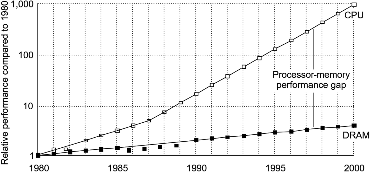 | ||
| Fig. 1 Processor-memory performance gap. | ||
The concept of computing-in-memory was developed in the last century, but the technology has not received much attention. The integration of computing power and storage units is costly and technically challenging. Integrated circuits are evolving at a rapid pace under Moore's Law. The needs of data processing are far from its limits. However, with the increased data volume and new demands for computing speed and accuracy, computing-in-memory technology is back in the spotlight. Computing-in-memory technology breaks through the traditional computing architecture, eliminating the need for a separate computing unit to process the data. The technology can be divided into charge-based and resistor-based storage technologies. Most of the charge-based storage technology is based on adding a computational circuit to a conventional memory cell, as shown in Fig. 2(b). For example, the SRAM memory cell is the central cell in a CMOS-based memory circuit. Simple logic circuits can be implemented by designing simple peripheral circuits, and efficient neural network training can also be achieved by SRAM across-array design. Resistor-based storage technologies use memory as the core of integrated circuits. The initial data for the system are the resistance values of the resistor cells, while the input data come from external electrical signals. The resistance value of each cell represents the final calculation result. Resistor-based circuits mainly use new non-volatile memories, such as RRAM, PCM, and FRAM. Advanced memory combined with an across-array structure enables complex computations such as vector-matrix multiplication, greatly accelerating computation speed and reducing operational power consumption. Resistor-based storage technologies will be described in detail below.
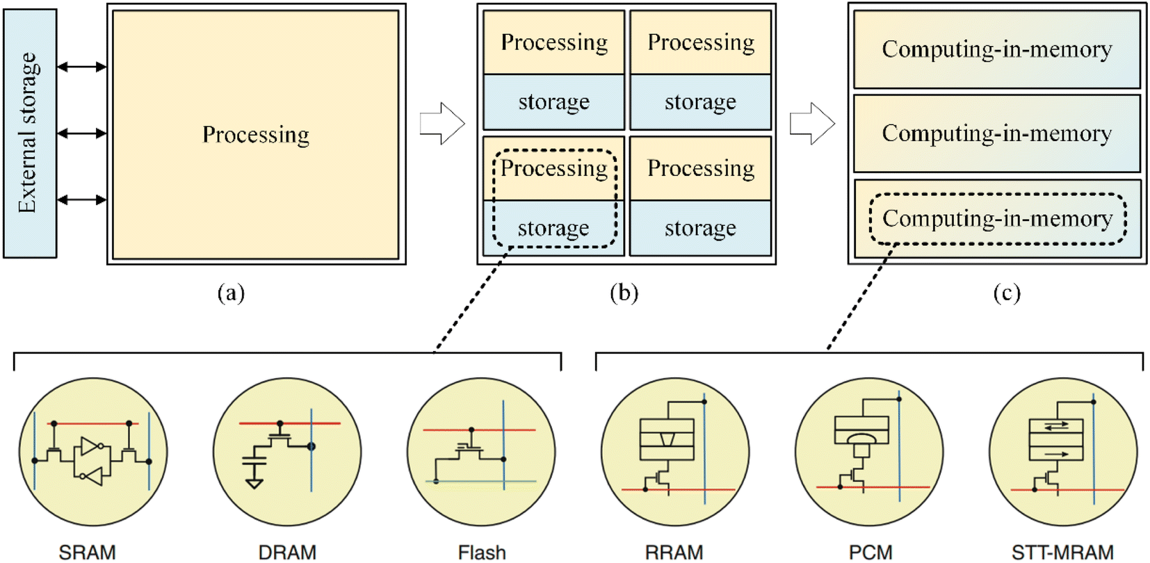 | ||
| Fig. 2 The development of the computing structure.21 (a) von Neumann architecture. (b) Near-memory computing structure. (c) Computing-in-memory structure. | ||
3 RRAM
3.1 Memristor
In 1971, Professor Chua10,22 of the University of California at Berwick introduced the memristor concept and then extended its definition. He considered that a memristor is the fourth fundamental circuit element in addition to resistance, capacitance, and inductance. The memristor complements the gap in the fundamental circuit relationship between charge and flux. Its mathematical model is represented by the ratio of magnetic flux to charge. The memristor resistance is numerically equal to the ratio of the voltage applied to memory terminals at a given moment to the current flowing through it. In practice, however, the value of a memristor is determined by the necessary amount of current or flux flowing through the memristor over time, which is a non-linear resistive element with memory characteristics.23The prevailing explanation for the resistive principle of the memristor is the wire filamentary resistive switching mechanism. The wire filament mechanism assumes that the resistance change of the device corresponds to the formation and rupture of wire filaments within the material.24 In most cases, a freshly prepared memristor usually exhibits fewer defects and shows an initial resistance state (IRS), as shown in Fig. 3(a). When a positive voltage is applied to the device, the conductive defects in the resistive layer are connected to form conductive filaments. The device's conductivity is enhanced, showing a low resistance state (LRS), as shown in Fig. 3(b). When a negative voltage is applied to the device, the conductive filaments break, and the device's conductivity is reduced, resulting in a high resistance state (HRS), as shown in Fig. 3(c). Some of the memristors even have intermediate resistance levels or more resistance levels.
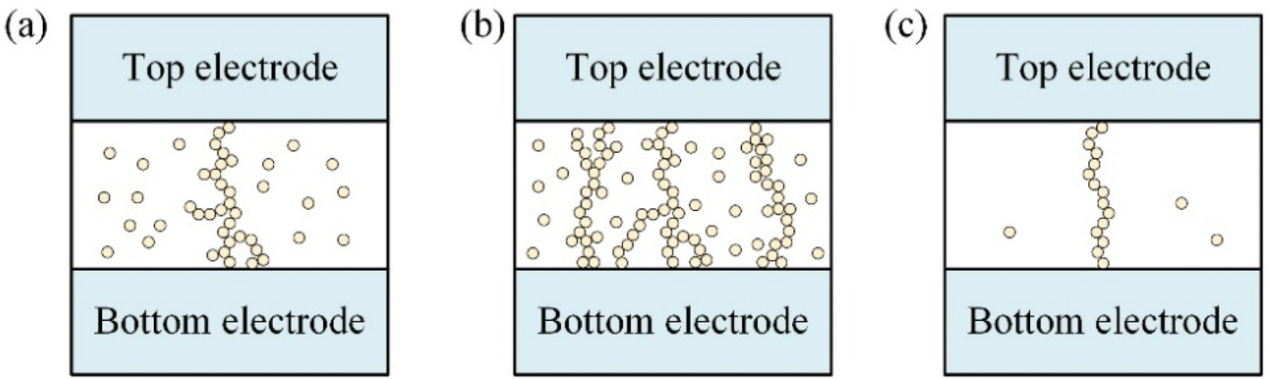 | ||
| Fig. 3 The wire filament mechanism. (a) Initial resistance state (IRS). (b) Low resistance state (LRS). (c) High resistance state (HRS). | ||
Researchers used the resistive properties of resistors to implement the calculation function. The memristor used in memory applications is called resistive random-access memory (RRAM). RRAM has high speed, high durability and multi-bit storage capability. It meets the development requirements of high capacity, high read and write times, faster read and write speeds, and lower power consumption. RRAM is expected to replace traditional storage devices to achieve a big boost in computing power.
3.2 Structure of RRAM
The basic structure of a memristor is a sandwich structure consisting of upper and lower metal electrodes and an intermediate insulator resistive layer. RRAM is constructed as an across-array structure to improve integration. Realization of high-density and reliable RRAM is crucial toward development of next-generation information storage and computing. The structure can be divided into active and passive arrays. In the active array, the RRAM forms an array with field effect tubes. The transistors control the reading, writing and erasing of resistive elements and can effectively isolate adjacent cells from interference. However, the active array design is complex and not conducive to integration. In passive arrays, each memory cell is defined by upper and lower electrodes formed by intersecting word and bit lines, as shown in Fig. 4(a). Passive arrays are used in most high-density RRAM arrays, and passive arrays are more conducive to the three-dimensional (3D) integration of the chip.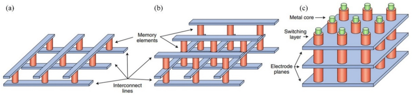 | ||
| Fig. 4 RRAM across-array architecture and scaling.25 (a) RRAM across-array structure with a single memory layer. (b) Horizontal stacked 3D across-array structure. (c) Vertical 3D across-array structure. | ||
The across-array structure of RRAM is one of the bases of its fast calculations and responsible calculations. Employing a 3D structure can make resource-expensive tasks into a manageable size and provides substantial improvement to the speed and energy efficiency while running complex neural network models. A broad range of applications can be envisioned with further optimizations in the device performance and more carefully designed on-chip peripheral analogue circuitry, even though the current 3D design might not be the most scalable architecture compared to its two-dimensional (2D) counterpart. According to the stacking form, 3D RRAM can be divided into a horizontal stacked 3D across-array structure (HRRAM) and vertical 3D across-array structure (VRRAM). HRRAM is composed of multilayer planar two-dimensional RRAM superimposed by the fabrication process, as shown in Fig. 4(b). VRRAM is made by rotating the conventional horizontal across-array structure by 90° and extending it repeatedly in the horizontal direction, as shown in Fig. 4(c).
Three-dimensional fabrication technology not only increases the integration of the chip and greatly reduces the chip area, but also increases the computing speed and brings newer applications. However, making 3D chips is still a very difficult process, and only a few labs can make them. In 2022, Tang et al.26 fabricated a RRAM across-array using MoS2 and then implemented a single three-dimensional RRAM cube by overlaying two-dimensional MoS2 layers, as shown in Fig. 5(a). This work paves the way algorithmically for the implementation of two memristors in high density neuromorphic computing systems. In the process, it is possible to integrate the prepared 2D RRAM into 3D successfully. However, 3D-HRRAM requires critical lithography and other processes for each stacked layer, and this overhead manufacturing cost increases linearly with the number of stacks. The three-dimensional vertical structure occupies a smaller area in the integrated array of the same number of devices and is suitable for large-scale operations. Huang et al.27 proposed a vertical architecture of RRAM design, as shown in Fig. 5(b). The RRAM is composed of graphene plane electrode/multilayer hexagonal boron oxide (h-BN) insulating dielectric stacked layers, AlOx/TiOx, a resistive switching layer and an ITO pillar electrode that exhibits reliable device performance. The vertical three-dimensional structure combining the graphene plane electrode with a multilayer h-BN insulating dielectric can pave the way toward a new area of ultra-high-density memory integration in the future. Q. Huo et al.28 reported a two-kilobit non-volatile CIM macro based on an eight-layer 3D VRRAM, as shown in Fig. 5(c). The chip is fabricated using a 55 nm complementary metal-oxide-semiconductor process. Scaling such systems to three-dimensional arrays could provide higher parallelism, capacity and density for necessary vector–matrix multiplication operations. Lin et al.29 successfully constructed an eight-layer array, as shown in Fig. 6(d). The 3D array was fabricated on top of a silicon wafer with a 100 nm thick thermally grown oxide layer. Researchers programmed parallelly operated kernels into the prepared RRAM, implemented a convolutional neural network and achieved software-comparable accuracy in recognizing handwritten digits.
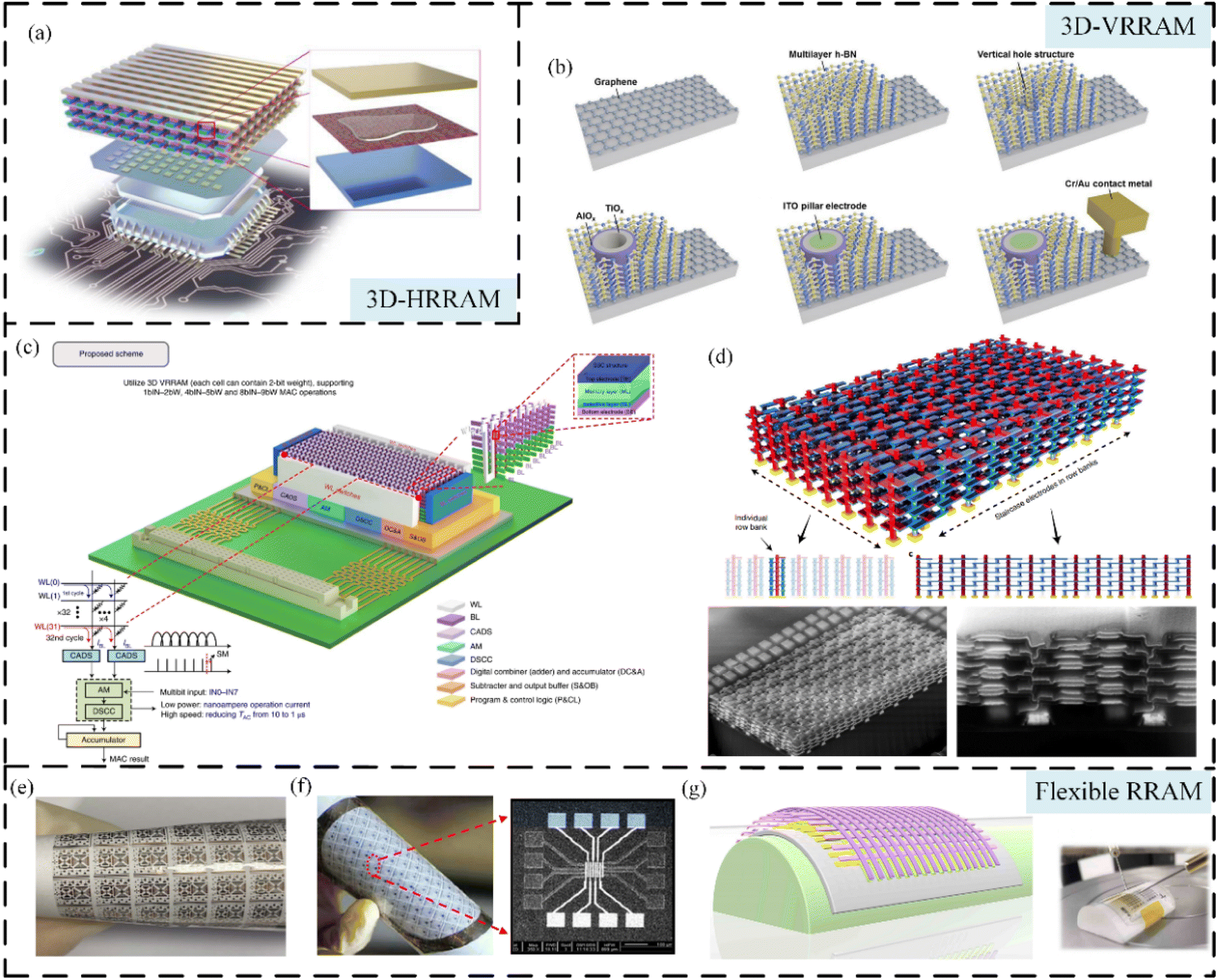 | ||
| Fig. 5 Different forms of RRAM. (a) 3D-HRRAM: a 3D memristor array with buried metal interconnects and logic circuits. (b–d): 3D-VRRAM. (b) The fabrication flows of a single 2D material based vertical RRAM. (c) High-precision CIM scheme based on MLSS 3D VRRAM. (d) 3D monolithic integrated memristor circuits. (e and f): Flexible RRAM. (e) Flexible RRAM crossbar arrays with a Ti/PPX-C/Cu structure. (f) The flexible memory devices based on polychord-para-xylylene. (g) 3D flexible RRAM artificial synaptic network using a low-temperature atomic layer. | ||
 | ||
| Fig. 6 Computing-in-memory realized by RRAM. (a) IMPLY logic and (b) NAND logic proposed by HP LABS. (c) The multi-functional boolean logic circuit schematic. (d and e): MAGIC logic computation. (d) MAGIC two-put OR gates and (e) NAND/NOR gates using the convert VTM method. (f–i): Complex computation. (f) Across-array circuits for cases beyond the constraints. (g) Memristor-based quinary half adder. (h) Two-bit adder circuit with parasitic elements based on RRAM. (i) Digital full adder based on RRAM. | ||
In addition, RRAM, made of flexible materials for particular application scenarios, is also a hot topic. Kim et al.30 used PPXC as a resistive switching layer and substrate to fabricate RRAM flexible across-arrays, as shown in Fig. 5(e). Researchers applied them to neuromorphic accelerated computing to test their performance with high electrical conductivity and durability. Huang et al.31 proposed a kind of single-component polymer RRAM based on polychord-para-xylylene, as shown in Fig. 6(f). The device has excellent chemical stability and high CMOS process compatibility as well as further reduced operation current. Wang et al.32 successfully prepared a 3-layer flexible RRAM array by a low-temperature atomic layer deposition technique to achieve high-density binary storage function and multi-bit storage in a single device, as shown in Fig. 5(g). Preparing flexible devices opens up new possibilities for future high-density, high-performance wearable applications.
A RRAM across-array can greatly compress the chip volume and improve the computing efficiency and computing volume. But the problem is also obvious: chip design and preparation processes are difficult, every application needs to be customized, there is still a lot of room for development and there are still unresolved problems.
(a) When writing and programming, current inevitably passes through other resistive cells. Leakage current can interfere with the accuracy of the information read when adding unnecessary power consumption.
(b) Due to the fabrication process, the ion movement pattern inside the device is somewhat random and not perfectly uniform for each resist-variable cell.33
(c) When the device is operating, thermal crosstalk affects the change in the resistance state of the surrounding resistive cells—leading to inaccurate calculations. The effect of thermal crosstalk even increases with increasing density.
4 Applications
RRAM is considered one of the outstanding candidates for emerging storage technologies. It has low power consumption, high speed computing, high density and non-volatile data storage capability. RRAM has been applied in logic computing, neural networks, brain-like computing, and fused technology of sense-storage-computing.4.1 Computing-in-memory
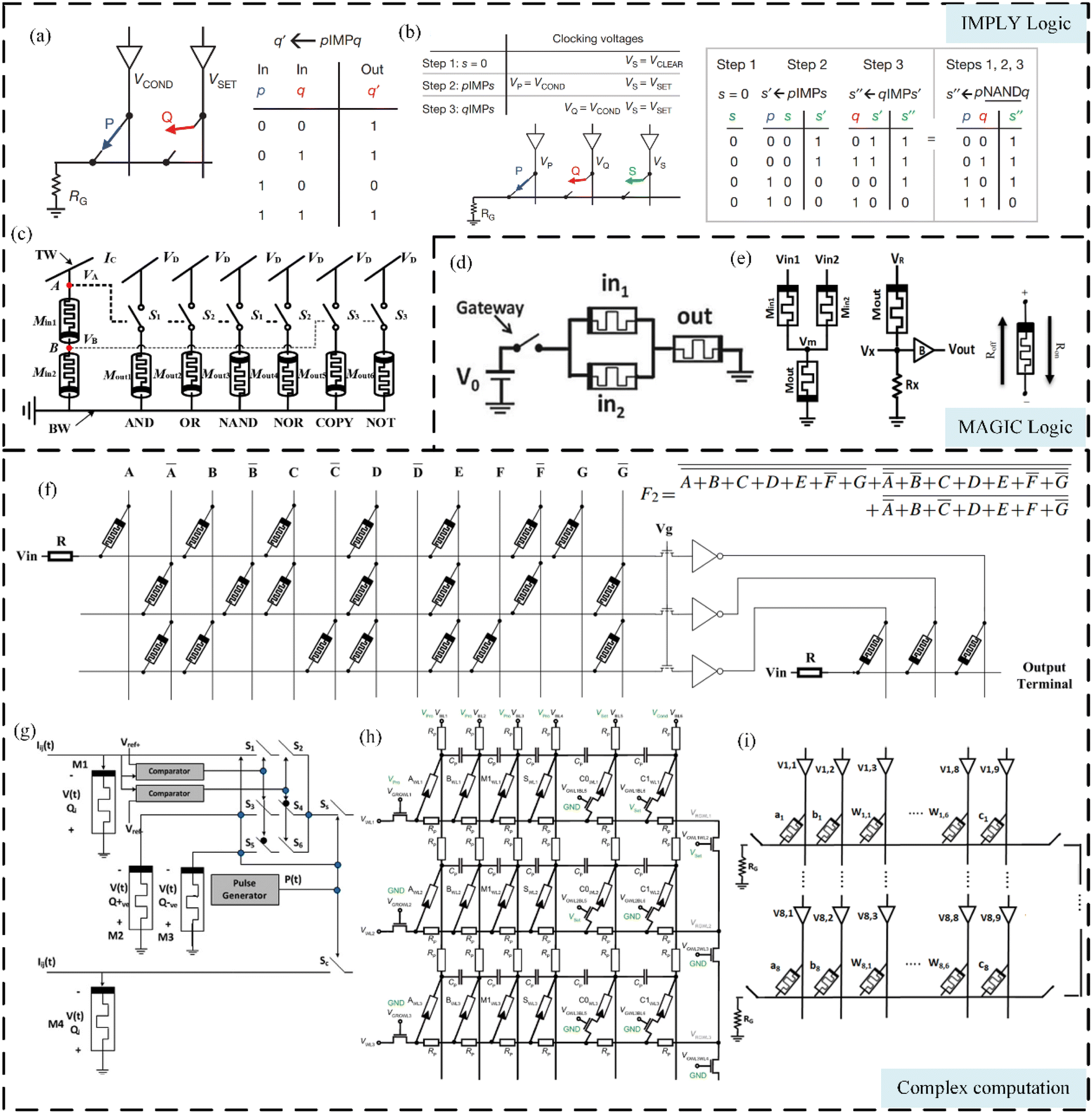
The simplest application is logic operations; the current application of logic circuits implemented logic gate operations using resistive cells instead of traditional transistors. HP LABS34 first prepared a physical model of RRAM in 2008 and implemented IMPLY logic operations. The primary logic cell and truth table are shown in Fig. 6(a). IMPLY and NOT logic can form a complete logic set to complete all 16 logics. However, it is not a beautiful operation, which destructs the input method because the final output of the implied logic overwrites the original input value. Implementing other logic using IMPLY logic also requires more steps, which is less efficient. Then, HP LABS also proposed the 3M1R structure, as shown in Fig. 6(b). It is an improvement to IMPLY, whose basic logic unit consists of three resistive cells and a voltage divider resistor. The high resistance state represents logic “1” and the low resistance state represents logic “0”, where P and Q represent the input variables and S represents the output variables. Based on the research from HP LABS, more complex logic operations can be obtained using RRAM. Dong et al.35 combined multiple logic resistors in a single circuit to implement logic operations, as shown in Fig. 6(c), which offers the possibility of implementing advanced computing architectures. The study implements two-input or multi-input AND, OR, NOR, and NAND operations and single-input copy and NOT operations. In each logic gate, the circuit uses non-volatile resistors of the RRAM as input and output states, thus enabling stateful logic operations. In contrast to several existing methods, this method generates a versatile state logic circuit that can perform multiple state logic operations simultaneously.In addition to the structure proposed by HP LABS, researchers connected RRAM in series and parallel. S. Kvatinsky et al.36 proposed a memristor-aided logic (MAGIC) circuit that uses resistive values as logical state variables, as shown in Fig. 6(d). Under applied voltage control, the five essential logic functions can be achieved by connecting the RRAM in series and parallel. This design approach allows the results of logic calculations to be stored in a separate resistive cell, avoiding the problem of data overwriting arising in IMPLY logic operation. F. Mozafari et al.37 proposed a new memristor-based NAND/NOR logic gate with a similar structure for general-purpose logic gates requiring two different input voltages. The structure consists of two input amnesia resistors and one output amnesia resistor, as shown in Fig. 6(e). RRAM-based logic calculations can reduce the computational complexity of the problem, as well as reduce the amount of data being accessed by performing the calculations within the across-array.
In recent years, the improvement of the technological level and the progress of materials research have enabled the successful preparation of larger RRAM matrices and the realization of more and more complex functions. Cui et al.38 proposed a family of NMOS-like RRAM gates. All gates are array implementable, and the gate family logic is complete. NOR, AND and NOR gates consume only one cycle during the computation phase. The gate circuit saves half the number of RRAM devices compared to its CMOS-based counterpart. By using RRAN gates and across-array structures, complex logic operations can be realized, as shown in Fig. 6(f). A. H. Fouad et al.39 proposed a multi-valued logic adder, as shown in Fig. 6(g). The study discussed the possibility of extending a three-valued adder circuit to a multi-valued logic adder theoretically. By exploiting the properties and dynamics of RRAM, the circuit achieved the advantages of handling different numbering systems, increasing density, and reducing processing time. Siemon et al.40 proposed a multi-input memristive switch logic, as shown in Fig. 6(h). This work enabled the function X OR (Y NOR Z) to be performed in a single step with three memristive switches. This OR/NOR logic gate increases the capabilities of memristive switches, improving the overall system efficiency of a memristive switch-based computing architecture. N. Taherinejad et al.41 present a new architecture for a digital full adder, as shown in Fig. 6(i). The circuit is faster than existing IMPLY-based serial designs while requiring less area compared to the existing parallel design.
In the latest studies, researchers hope not only to implement logical operations, but also to implement complex mathematical analysis in RRAM across-arrays. Tian et al.42 realized a hardware Markov chain algorithm in a single device for machine learning. M. Teimoory et al.43 designed a 2 × 2 multiplier circuit, as shown in Fig. 7(a). The circuit requires only sixteen resistive cells, eight transistors, and only one calculation time step for the multiplication operation, which is of low cost. B. Chakrabarti et al.44 demonstrated vertical monolithic integration of 3D RRAM crossbars on a foundry-processed 5 × 5 CMOS chip. The chip can realize dot-product operation, which is the first application of functional 3D CMOL hybrid circuits. Xie et al.45 used h-BN RRAM across-arrays to demonstrate the hardware implementation of dot product operation and the linear regression algorithm, as shown in Fig. 7(b)–(d). Y. Halawani et al.46 proposed an XNOR-based RRAM content addressable memory (CAM) with an analog time-domain adder function for efficient winning class computation, as shown in Fig. 7(e). The chip had 31 times less area and about three times less energy consumption than state-of-the-art RRAM designs. P. Kumar et al.47 used h-BN as an electrolyte to implement the fabrication of an across-array RRAM, as shown in Fig. 7(f), and combined it with CMOS circuits to implement extreme learning machine algorithms. With CMOS, circuits implement the encoder unit and RRAM arrays implement the decoder unit. The hybrid architecture performs well on complex audio, image and non-linear classification tasks with real-time data sets.
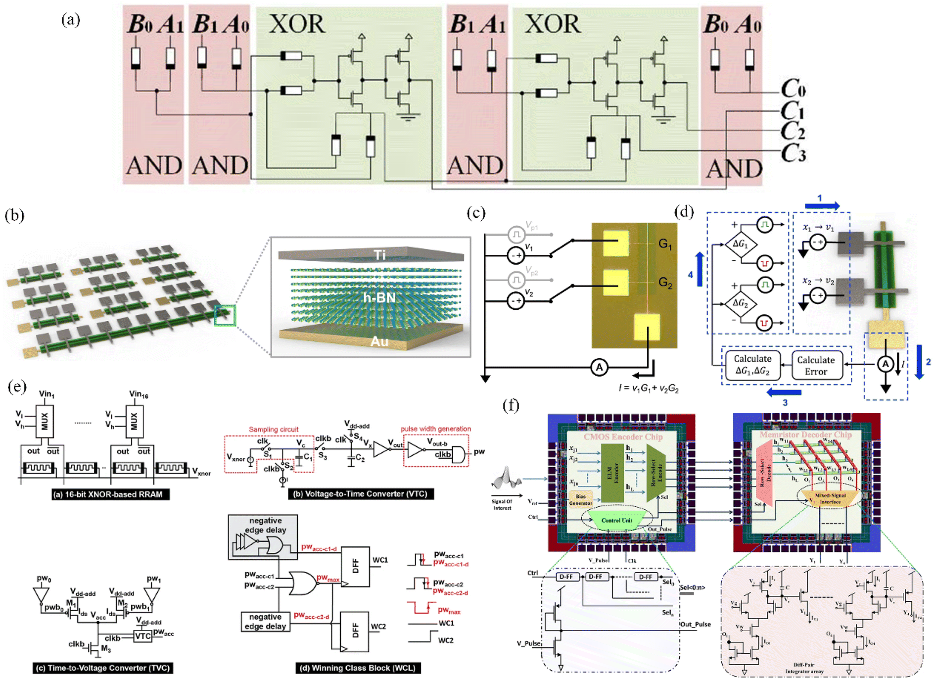 | ||
| Fig. 7 Complex mathematical formulas realized by RRAM. (a) Logic design of the 2 × 2 multiplier. (b) Schematic of Au/h-BN/Ti RRAM arrays and cross-sectional schematic of a single memristor. (c) Schematic of the experimental setup for demonstration of basic dot-product operation on h-BN RRAM arrays. (d) Flow diagram for stochastic multivariable linear regression. (e) Circuit designs of the proposed RRAM-based CAM, analog time-domain adder and winning class logic. (f) System architecture showing a CMOS encoder chip and memristor decoder chip along with its functional sub-blocks. | ||
These studies are of great significance for further implementation of neuromorphic computing and machine learning hardware based on RRAM across-arrays. The compatibility of the above design with CMOS technology provides a new way for the development of digital logic circuits. Introduction of RRAM was presented as a solution to the fundamental limitations of VLSI systems.
4.2 Neural networks and brain-like computing
In recent years, RRAM has been widely used in neural morphological networks. Artificial neural networks and all their variants are the primary tools for machine learning tasks. The continuous production of large amounts of data makes it possible to train and operate artificial neural networks successfully. However, in order to achieve high inference accuracy, neural networks usually require a large number of parameters. The traditional structure of memory and computing points makes the whole stage consume a lot of time and energy but using RRAM to build neural networks is expected to solve this problem. RRAM has resistive properties and is similar to synapses in neural networks, so the neural network hardware and a neural network model based on RRAM have intrinsic consistency. A single device can be used as a synapse and can integrate storage and operation. A RRAM-based neural network integrates computing and storage closely, eliminating data transmission between the processor and memory, thus improving the overall system performance and saving most system energy consumption. RRAM is well compatible with CMOS processes and can be scaled up on a large scale through cross-array structures. Through CMOS processes, functional circuits are added to the periphery of RRAM, so that the system can complete the calculation of a matrix in one operation, thus playing an important role in high dimensional computation.The perceptron model is an early neural network algorithm. In the calculation process of the perceptron neural network, matrix vector multiplication between the input information vector and weight matrix consumes a lot of computing resources. However, using RRAM across-arrays to realize matrix vector multiplication in parallel in one step can greatly reduce the energy consumption of the hardware neural network. The RRAM across-array is used to store the synaptic weight matrix, and the conductance at each crossing is used to represent the weight value of a synaptic connection. MNIST image classification is modeled using a single-layer perceptron that is not in situ trained and a large-scale multi-layer perceptron classifier based on a more advanced conductance tuning algorithm. M. Prezioso et al.48 first produced an across-array of RRAMs for neural network computing. Researchers used a 12 × 12 RRAM across-array to form a single-layer perceptron network to recognize and classify black and white letters in 3 × 3 pixels, as shown in Fig. 8(a). F. M. Bayat et al.49 produced two 20 × 20 RRAM across-array, as shown in Fig. 8(d), and integrated them with discrete CMOS components on two printed circuit boards to implement a multilayer perceptron (MLP) neural network. The MLP network has 16 inputs, 10 hidden layer neurons, and 4 outputs, enough to classify 4 × 4 pixel black and white patterns into 4 categories. Then, more complex array structures were proposed based on previous research to realize much more complex computing. H. Kim et al.50 developed a 64 × 64 passive crossbar circuits with almost 99% working cross point metal-oxide memristors based on the foundry-compatible fabrication process. The circuit has a relatively average error of <4% when programming 4 K grey-scale patterns and an error of nearly 1%. It is an essential step towards realizing a human brain-scale integrated neuromorphic system.
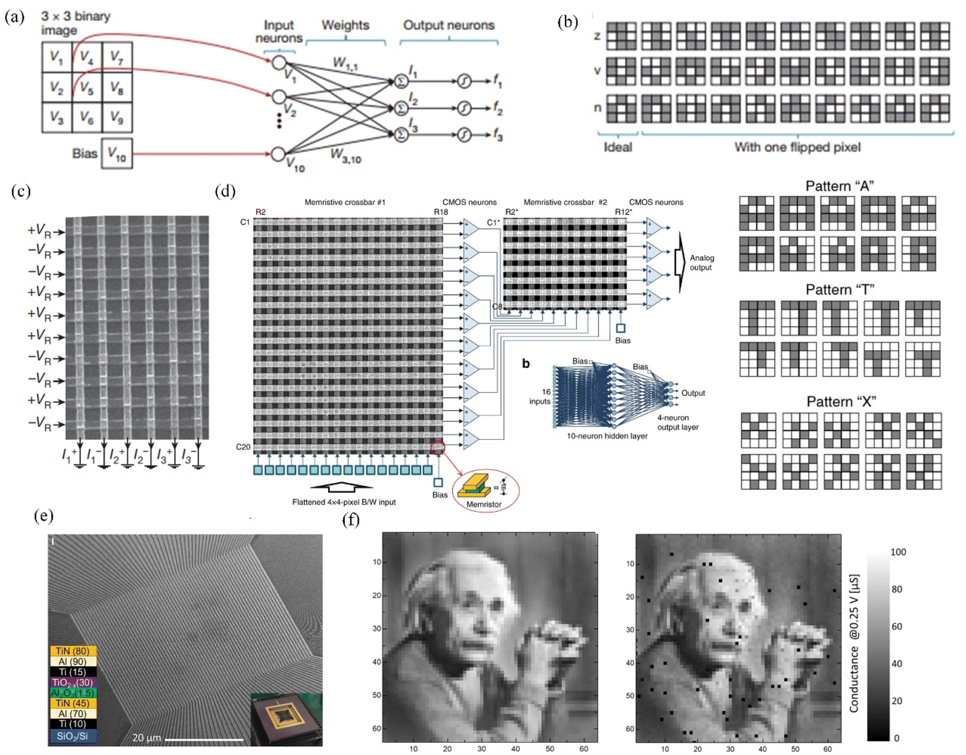 | ||
| Fig. 8 Perceptron network based on RRAM. (a–c): Single-layer perceptron network. (a) Top-level description of the network. (b) The used input pattern set. (c) 12 × 12 RRAM across-array circuit. (d–f): Multilayer perceptron network. (d) Double layer 20 × 20 RRAM across-array circuit combined with the CMOS process. (e) 64 × 64 RRAM passive across-array circuit. (f) Programming Einstein image to (e) with a 5% relative error. | ||
The convolutional neural network (CNN) reduces the dimensions by convolutional operation, reduces parameter complexity, simplifies complex problems before processing, and greatly reduces the calculation cost. The convolutional neural network based on memristor cross arrays mainly consists of two parts: the convolutional operation part and the fully connected layer part. On the one hand, the memristor array can store convolution kernels and complete the matrix vector multiplication of input information and convolution kernels in one step, which greatly improves the computational efficiency. On the other hand, the fully connected layer part of a convolutional neural network is a multi-layer perceptron, which can also be realized in parallel by using the memristor cross array as mentioned above. However, CNNs have not yet fully implemented hardware via a RRAM across-array. P. Yao et al.51 implemented complete hardware for convolutional networks based on RRAM array chips. The team used eight arrays with 2048 RRAM to implement a five-layer convolutional neural network. The chip was two orders of magnitude more energy efficient than an image processor (GPU) in processing convolutional neural networks by comparison with conventional neural network computation.
Stochastic neural networks introduce random changes into neural networks, one is to assign transfer functions of the stochastic process among neurons and the other is to assign random weights to neurons. This makes stochastic neural networks very useful in optimization problems, because random transformations avoid local optimality. The key operation in stochastic neural networks is the random dot product, which has become the latest method to solve the problems of machine learning, information theory and statistics. Although there have been many demonstrations of dot product circuits and random neurons, there is still a lack of efficient hardware implementation combining these two functions. M. R. Mahmoodi et al.52 proposed versatile stochastic dot product circuits based on nonvolatile memories for high performance neuro-computing and neuro-optimization, as shown in Fig. 9. F. Zahari et al.53 proposed an analogue pattern recognition with stochastic switching binary CMOS-integrated RRAM. Researchers prepared a random binary RRAM device based on a polycrystalline HfO and have produced software neurons. Based on this, a random neural network is used for image recognition. The convergence rate of this new learning algorithm is very fast, which may significantly reduce the power consumption of the system. This study has potential applications in stochastic neural networks to solve MNIST pattern recognition tasks.
 | ||
| Fig. 9 Stochastic neural networks.52 (a) Stochastic dot-product circuit and its applications in neurocomputing. (b) RRAM-based restricted Boltzmann machine. (c) A bipartite graph of the considered RBM network and its implementation (the red rectangle highlights the utilized area of a 20 × 20 across-array). | ||
Reservoir computing (RC) is a concept developed from recursive neural networks (RNNs) that has recently been successfully used to implement a wide range of tasks, such as image model recognition, time series prediction, and pattern generation. Researchers have successfully used memristors for this purpose as well. Fig. 10 shows the concept of a memristor-based RC system. The spikes collected from firing neurons are used directly as inputs to an excitation memristor. The repository space is further extended with the concept of virtual nodes to help handle complex time inputs. A simple neural network is used as the reservoir's readout layer to produce the final output. In 2020, Lu et al.54 looked at reserve pool arithmetic. Researchers demonstrate a RC system based on RRAM, whose states reflect the temporal characteristics of nerve peak sequences, successfully used to identify neural firing patterns, monitor the conversion of firing patterns, and identify neural synchronization states between different neurons. This work makes it possible to realize efficient neural network signal analysis with high spatial and temporal accuracy. In addition, researchers made a RRAM across-array based on WOx. They used a circuit to form an array to recognize digits and increased the noise, proving the anti-interference and stability of the system's recognition, and expanded to a small reserve pool composed of 88 memristors for handwritten digit recognition. X. Liang et al.55 also applied RRAM to reservoir computing, an artificial neural network for efficient processing of temporal signals, with the potential to have a significant impact in the field of brain-like computing.
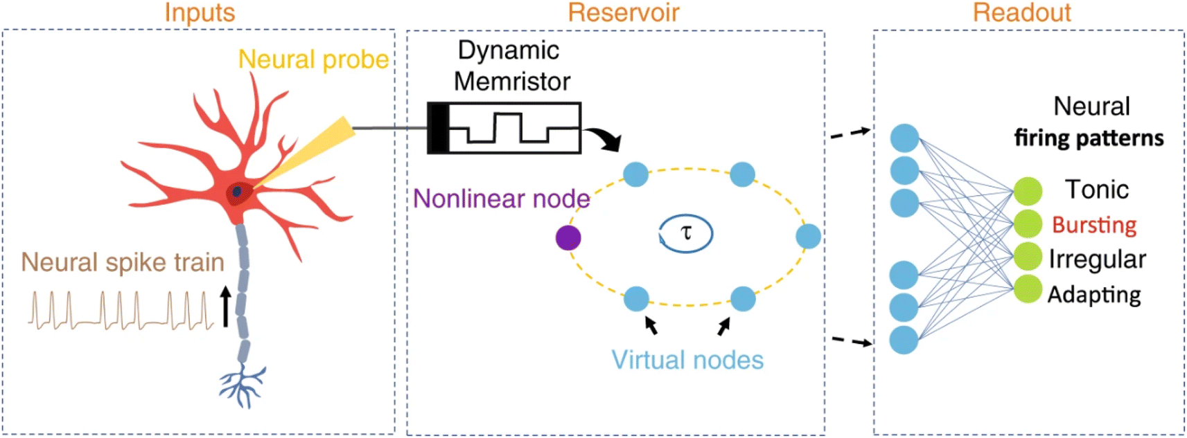 | ||
| Fig. 10 Schematic showing the concept of a memristor-based RC system for neural activity analysis. | ||
On the basis of the development of neural networks, the concept of brain-like computing has been put forward. From an information technology perspective, researchers have abstracted the way decisions are made in the human brain. They connected it through multi-layered artificial neural networks to create a non-linear, adaptive computing model for information processing. Wu et al.56 have been focusing on research on brain-like computing for a long time and have described the RRAM-based brain-like circuit in detail, as shown in Fig. 11(a). By introducing artificial dendritic computational units with rich dynamic properties, the team constructed a novel artificial neural network,57 significantly reducing system power consumption while improving computational network accuracy. Compared to traditional processes, the new system has a 30 times reduction in dynamic power consumption, an 8% increase in accuracy, and an overall system power consumption downgraded by three orders of magnitude. Z. Wu et al.58 built an artificial sensory neural system implementation scheme with habituation properties based on RRAM, as shown in Fig. 11(b). The system used habituation as a biological learning rule to build a habituated impulse neural network that can be applied to robot autonomous cruising obstacle avoidance. The neural network can be used to implement robot obstacle avoidance functions and effectively improve robot obstacle avoidance efficiency.
 | ||
| Fig. 11 Brain-like computing. (a) Neural network operations using RRAM implementation. (b) Biological afferent nerve vs. the artificial afferent nerve. | ||
The application of RRAM-based neural networks is an indispensable research direction in neuromorphic computing. As a new type of synaptic device, the memristor realizes the hardware mapping of the synaptic weight well by means of multivalue modulation under pulse and can store the synaptic weight matrix and realize in situ calculations. The parallel matrix multiplication and addition capability of the across-array structure of RRAM realizes the acceleration of neural network computing and provides a solution for constructing a new computing architecture.
4.3 Fused technology of sense-storage-computing
The human nervous system senses the physical world in an analogue but efficient way. Researchers have been working on using hardware to simulate human perceptual systems. Sensors take signals such as light, pressure and sound and convert them into electrical signals. The processor is used to analyze electrical signals and simulate human sensory systems. However, traditional computing platform analysis speed is slow and precision is not high. As a new type of memory, RRAM can be made of materials that are sensitive to peripheral signals and can itself be used as a sensor. In addition, RRAM can combine microsensors with neural network computing. The sense-storage-computing fusion technology based on RRAM brings a new research direction for bionics technology.Visual perception is made by using the effect of light signals on RRAM or using the RRAM across-array as a processing circuit, which can currently be used to identify numbers and test light intensity. Emboras et al.59 first discovered the change in light signal transmission in the waveguide during transformation, which laid the foundation for visual perception based on RRAM. Zhou et al.60 prepared a photo-resistive memory, as shown in Fig. 12(a) and (b). The component can convert light signals into electrical signals and store the data briefly. In conjunction with developments in neural networks, researchers used RRAM as a synaptic node to enable more advanced visual processing. Lorenzi et al.61 used an RRAM array to recognize a 5 × 5 pixel binary picture. Sarkar et al.62 used an RRAM-based neuromorphic circuit system and trained and tested the system to successfully recognize basic Arabic numerals. Not only digital numbers, but also visual recognition of infrared, low light and images are currently being investigated.
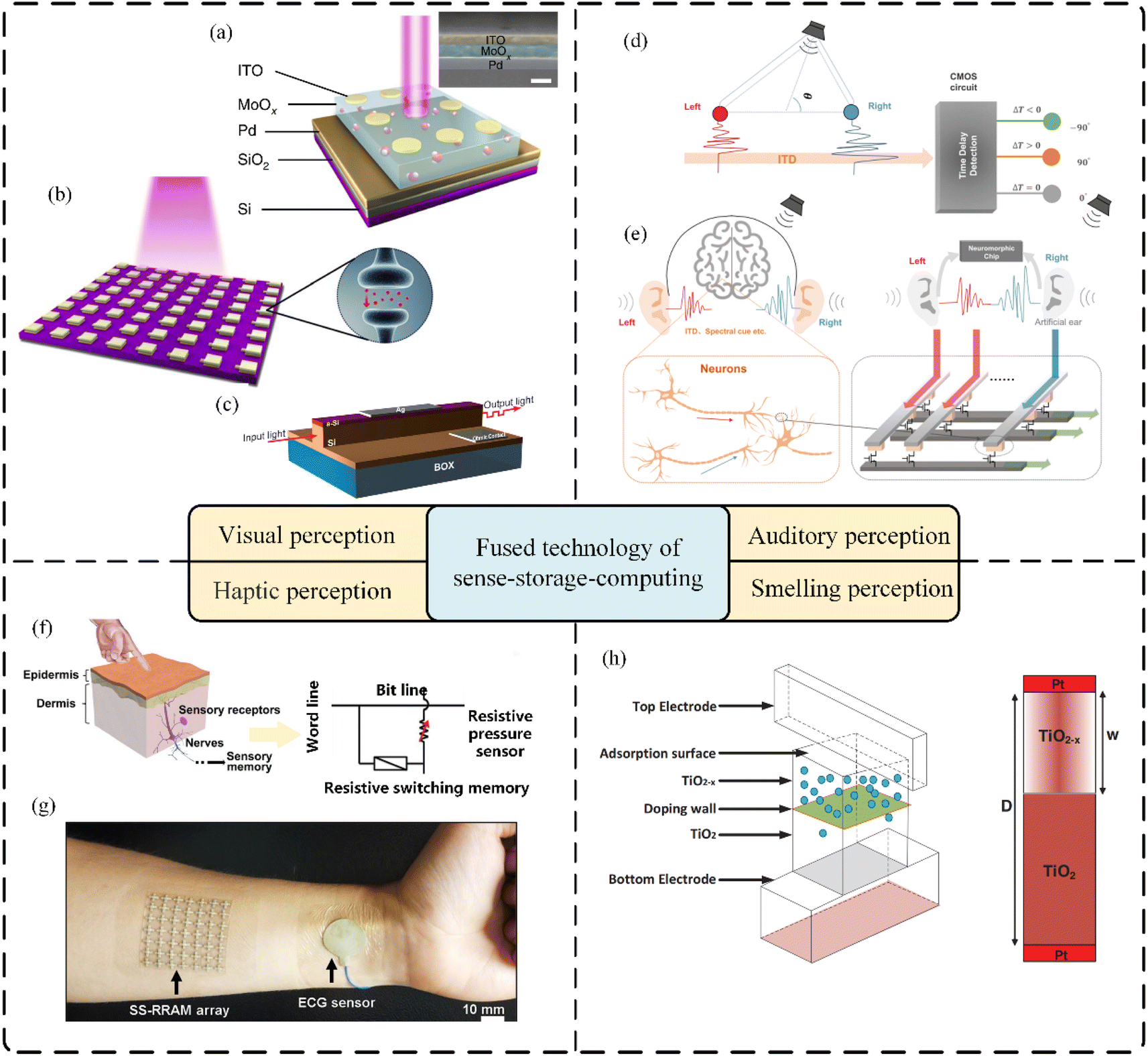 | ||
| Fig. 12 Fused technology of sense-storage-computing. (a) Schematic structure of ORRAM. (b) Schematic structure of an 8 × 8 ORRAM array. (c) Three-dimensional schematic of the investigated optically readable plasmonic RRAM.59 (d) The common implementation scheme for sound localization application with CMOS circuits. (e) A conceptual diagram of a memristor-based neuromorphic sound localization system. The RRAM across-array acts as synapses to deal with binaural sound signals. (f) The conceptual diagram of haptic memory. (g) Image for 7 × 7 SS-RRAM arrays and ECG electrode mounted onto the wrist. (h) Structure of a memristor for gas sensing applications. | ||
In terms of sound localization, researchers have localized the location of sound sources based on the theory of interaural time difference, where the time difference between the theoretical sound arriving in the two ears is shown in Fig. 12(d). Gao et al.63 have a leading study in this area. The team fabricated a 128 × 8 array of memristors and proposed a new sound localization algorithm. The devices were tested with pulses to simulate sound signals, showing that the training accuracy and energy consumption of the system built using the memristor array were significantly improved, representing a significant advance in auditory localization systems with memristors. F. Moro et al.64 designed an event-driven object localization system inspired by the owl auditory cortex using a combination of state-of-the-art piezoelectric micromechanical ultrasound sensors and RRAM. The system was more efficient and power-efficient than microcontrollers performing the same task by several orders of magnitude.
Haptic perception is mainly studied in terms of sensing external pressure, where pressure data are converted into electrical signals and stored in memory. The location of pressure generation can be clarified through an array mechanism of resistive variable memory, as shown in Fig. 12(f). Park et al.65 used a flexible RRAM array for ECG measurements, as shown in Fig. 12(g). Researchers successfully demonstrated stable data storage of cardiac signals, a damage-reliable memory triggering system using a triboelectric energy-harvesting device, and touch sensing via pressure-induced resistive switching.
As for smelling perception, the research started late, and the system can identify a small type of gas. People use the combination of a gas sensor and RRAM made of special materials and use the storage array to store and process the data quickly, so as to achieve the purpose of recognition. A. Adeyemo et al.66 used an across-array RRAM as a gas sensor, as shown in Fig. 12(h). Researchers used the HP LABS fabricated TiO2 based memristor model in an attempt to improve sensing accuracy. The experiment provides the basis for the research of smelling perception. At present, the smell sensing system using RRAM has a long sensing period, low sensing accuracy, single sensing gas, and narrow application. Most systems have a small response gap when identifying similar gases, which requires additional amplifying circuits to be sufficient for classification, increasing the structural complexity.
4.4 Other applications
RRAM has good switching and isolation characteristics for high-frequency communications. In 5G communication, the RRAM has 50 times the switching efficiency of other non-volatile switches. At 6G operating frequencies, RRAM also exhibits high isolation and has sub-nanosecond pulse switching, low BER and a high signal-to-noise ratio. M. Kim et al.67–69 worked on RRAM for high-frequency applications at the University of Texas. RRAM made from MoS2 and h-BN is suitable as an energy-efficient RF switch, overcoming the limitations of transistors and pick-and-place switches. Researchers also predicted that RRAM could be used in mobile systems, low-power IoT and terahertz beam steering. The unique switching randomness of RRAM has important applications in information security and can also be used to design chaotic circuits. H. M. Ibrahim et al.70 have implemented a robust and lightweight physically unclonable function (PUF) architecture using RRAM, with implications for cryptographic key and security application upgrades. In addition, P. S. Zarrin et al.71 proposed a neuromorphic on-chip recognition of saliva samples of COPD and healthy controls using RRAM. This is an application of RRAM in the medical field.5 Conclusion and outlook
With the constraints of the von Neumann structure and the physical limits of semiconductor processing, computers are experiencing bottlenecks in their ability to process data. As a new computing principle, computing-in-memory technology embeds the computation capability into the storage unit. This increases computation speed, reduces system power consumption, and opens up more application possibilities.RRAM is a new memory type with resistive and non-volatile properties. The structure, mechanism and preparation of RRAM have been the focus of attention, with research continuing in in-memory logic operations, brain-like computing and fused technology of sense-storage-computing. However, research into RRAM still faces some challenges:
(a) RRAM has randomness. The characteristics presented by memory resistors are not identical from cycle to cycle. There is also variability in devices made from the same batch. The preparation process of RRAM is being improved to try to solve this problem. In addition, the addition of peripheral circuits to the memristor array, the use of check methods and redundant design are also used to reduce errors.
(b) The best materials for the resistive layer in RRAM are also being screened. Metal oxides, 2d materials, emerging materials and organics are currently used for the preparation of RRAM. The materials used to prepare devices largely influence the performance of amnesic resistors. High resistance ratios, good homogeneity and matching proven manufacturing processes and equipment are the basis for judging the suitability of the material. We need to develop new materials with innovative approaches and explore the best material composition ratios based on already well-defined material elements. Better materials will enhance the performance given to each application.
(c) Mass production is almost impossible to replace most conventional memories. Across-array circuits are still in the small-scale laboratory stage. The preparation of memristors is difficult, with only a few laboratories and processors meeting the demand. The variety of materials used in the preparation of memristors and the preparation processes involved each have their own characteristics, and integration with existing mature processes takes time. Complex functional applications require customization. Different functions can be achieved by selecting different memory resistor units.
Data availability
The data that support the findings of this study are available from the corresponding author upon reasonable request.Conflicts of interest
The authors declare that they have no known competing financial interests or personal relationships that could have appeared to influence the work reported in this paper.Acknowledgements
This research was supported by the National Natural Science Foundation of China under Grant 61971389, Grant 62131010, and Grant 61801253 and in part by the Zhejiang Provincial Natural Science Foundation of China under Grant LR22F010001, Grant LZ20F010006, Grant LY20F010003 and LY21F010006 and the Fundamental Research Funds for the Provincial Universities of Zhejiang Grant 2020YW01.References
- M. Lundstrom, Moore’s Law Forever, Science, 2003, 299(5604), 210–211 CrossRef CAS PubMed.
- R. R. Schaller, Moore's law: past, present and future, IEEE Spectrum, 1997, 34(6), 52–59 Search PubMed.
- J. Sim, M. Kim, Y. Kim, et al., MAPIM: Mat Parallelism for High Performance Processing in Non-volatile Memory Architecture; Proceedings of the 20th International Symposium on Quality Electronic Design (ISQED), F 6-7 March 2019, 2019 Search PubMed.
- W. H. Kautz, Cellular Logic-in-Memory Arrays, IEEE Trans. Comput., 1969, C-18(8), 719–727 Search PubMed.
- A. Jaiswal, I. Chakraborty and A. Agrawal, et al., 8T SRAM Cell as a Multibit Dot-Product Engine for Beyond von Neumann Computing, IEEE Transactions on Very Large Scale Integration (VLSI) Systems, 2019, 27(11), 2556–2567 Search PubMed.
- R. Guo, L. You and Y. Zhou, et al., Non-volatile memory based on the ferroelectric photovoltaic effect, Nat. Commun., 2013, 4(1), 1990 CrossRef PubMed.
- M. Wuttig and N. Yamada, Phase-change materials for rewriteable data storage, Nat. Mater., 2007, 6(11), 824–832 CrossRef CAS PubMed.
- W. Li, X. Qian and J. Li, Phase transitions in 2D materials [J], Nat. Rev. Mater., 2021, 6(9), 829–846 CrossRef CAS.
- C. Chappert, A. Fert and F. N. Van Dau, The emergence of spin electronics in data storage, Nat. Mater., 2007, 6(11), 813–823 CrossRef CAS PubMed.
- L. Chua, Memristor-The missing circuit element [J], IEEE Trans. Circuit Theory, 1971, 18(5), 507–519 Search PubMed.
- D. Strukov, G. Snider and D. Stewart, et al., The Missing Memristor Found, Nature, 2008, 453, 80–83 CrossRef CAS PubMed.
- I. Hossen, M. A. Anders and L. Wang, et al., Data-driven RRAM device models using Kriging interpolation, Sci. Rep., 2022, 12(1), 5963 CrossRef CAS PubMed.
- J. Kang, T. Kim and S. Hu, et al., Cluster-type analogue memristor by engineering redox dynamics for high-performance neuromorphic computing, Nat. Commun., 2022, 13(1), 4040 CrossRef CAS PubMed.
- D. Ielmini, Resistive switching memories based on metal oxides: mechanisms, reliability and scaling, Semicond. Sci. Technol., 2016, 31(6), 063002 CrossRef.
- S. Thomas, IGZO and RRAM team up, Nat. Electron., 2020, 3(7), 353 CrossRef.
- E. C. Ahn, H. S. P. Wong and E. Pop, Carbon nanomaterials for non-volatile memories, Nat. Rev. Mater., 2018, 3(3), 18009 CrossRef CAS.
- S. Bulja, R. Kopf and A. Tate, et al., High frequency resistive switching behavior of amorphous TiO2 and NiO, Sci. Rep., 2022, 12(1), 13804 CrossRef CAS PubMed.
- H. S. P. Wong and S. Salahuddin, Memory leads the way to better computing, Nat. Nanotechnol., 2015, 10(3), 191–194 CrossRef CAS PubMed.
- M. Horowitz. 1.1 Computing's Energy Problem (And what We Can Do about it) [M]. 2014 Search PubMed.
- D. Patterson, T. Anderson and N. Cardwell, et al., A case for intelligent RAM, IEEE Micro, 1997, 17(2), 34–44 CrossRef.
- A. Sebastian, M. Le Gallo and R. Khaddam-Aljameh, et al., Memory devices and applications for in-memory computing, Nat. Nanotechnol., 2020, 15(7), 529–544 CrossRef CAS PubMed.
- L. Chua, If it’s pinched it’s a memristor, Semicond. Sci. Technol., 2014, 29(10), 104001 CrossRef.
- L. Chua. Everything You Wish to Know About Memristors but Are Afraid to Ask [M]//CHUA L, SIRAKOULIS G C, ADAMATZKY A, Handbook of Memristor Networks, Springer International Publishing, Cham, 2019, pp. 89–157 Search PubMed.
- Y. Li, S. Long and Y. Liu, et al., Conductance Quantization in Resistive Random Access Memory, Nanoscale Res. Lett., 2015, 10(1), 420 CrossRef PubMed.
- D. Ielmini and H. S. P. Wong, In-memory computing with resistive switching devices, Nat. Electron., 2018, 1, 333–343 CrossRef.
- B. Tang, H. Veluri and Y. Li, et al., Wafer-scale solution-processed 2D material analog resistive memory array for memory-based computing, Nat. Commun., 2022, 13(1), 3037 CrossRef CAS PubMed.
- Y.-J. Huang and S.-C. Lee, Graphene/h-BN Heterostructures for Vertical Architecture of RRAM Design, Sci. Rep., 2017, 7(1), 9679 CrossRef PubMed.
- Q. Huo, Y. Yang and Y. Wang, et al., A computing-in-memory macro based on three-dimensional resistive random-access memory, Nat. Electron., 2022, 5(7), 469–477 CrossRef.
- P. Lin, C. Li and Z. Wang, et al., Three-dimensional memristor circuits as complex neural networks, Nat. Electron., 2020, 3(4), 225–232 CrossRef.
- J. E. Kim, B. Kim and H. T. Kwon, et al., Flexible Parylene C-Based RRAM Array for Neuromorphic Applications, IEEE Access, 2022, 10, 109760–109767 Search PubMed.
- R. Huang, Y. Cai, Y. Liu, et al., Resistive Switching in Organic Memory Devices for Flexible Applications [M], 2014 Search PubMed.
- T. Wang, J. Meng and L. Chen, et al., Flexible 3D memristor array for binary storage and multi-states neuromorphic computing applications, InfoMat, 2020, 3, 212–221 CrossRef.
- J. Guy, G. Molas, E. Vianello, et al., Investigation of the physical mechanisms governing data-retention in down to 10nm nano-trench Al2O3/CuTeGe conductive bridge RAM (CBRAM); Proceedings of the 2013 IEEE International Electron Devices Meeting, F 9-11 Dec. 2013, 2013 Search PubMed.
- J. Borghetti, G. Snider and P. Kuekes, et al., Memristive switches enable stateful logic operations via material implication, Nature, 2010, 464, 873–876 CrossRef CAS PubMed.
- L. Luo, Z. K. Dong and S. K. Duan, et al., Memristor-based stateful logic gates for multi-functional logic circuit, IET Circuits Devices Syst., 2020, 14(6), 811–818 CrossRef.
- S. Kvatinsky, D. Belousov and S. Liman, et al., MAGIC—Memristor-Aided Logic, IEEE Trans. Circuits Syst. II Express Briefs., 2014, 61(11), 895–899 Search PubMed.
- F. Mozafari, M. J. Sharifi, A. Ahmadi, et al., A Novel Architecture for Memristor-Based Logic; Proceedings of the 2021 IEEE International Midwest Symposium on Circuits and Systems (MWSCAS), F 9-11 Aug. 2021, 2021 Search PubMed.
- X. Cui, Y. Ma and F. Wei, et al., The Synthesis Method of Logic Circuits Based on the NMOS-Like RRAM Gates, IEEE Access, 2021, 9, 54466–54477 Search PubMed.
- A. H. Fouad and A. G. Radwan, Memristor-based quinary half adder, AEU - Int. J. Electron. Commun., 2019, 98, 123–130 CrossRef.
- A. Siemon, R. Drabinski and M. J. Schultis, et al., Stateful Three-Input Logic with Memristive Switches, Sci. Rep., 2019, 9(1), 14618 CrossRef CAS PubMed.
- N. Taherinejad, T. Delaroche, D. Radakovits, et al.A Semi-serial Topology for Compact and Fast IMPLY-Based Memristive Full Adders [M]. 2019 Search PubMed.
- H. Tian, X.-F. Wang and M. A. Mohammad, et al., A hardware Markov chain algorithm realized in a single device for machine learning, Nat. Commun., 2018, 9(1), 4305 CrossRef PubMed.
- M. Teimoory, A. Amirsoleimani, A. Ahmadi, et al., A hybrid memristor-CMOS multiplier design based on memristive universal logic gates; Proceedings of the 2017 IEEE 60th International Midwest Symposium on Circuits and Systems (MWSCAS), F 6-9 Aug. 2017, 2017 Search PubMed.
- B. Chakrabarti, M. A. Lastras-Montaño and G. Adam, et al., A multiply-add engine with monolithically integrated 3D memristor crossbar/CMOS hybrid circuit, Sci. Rep., 2017, 7(1), 42429 CrossRef CAS PubMed.
- J. Xie, S. Afshari and I. Sanchez Esqueda, Hexagonal boron nitride (h-BN) memristor arrays for analog-based machine learning hardware, npj 2D Mater. Appl., 2022, 6(1), 50 CrossRef CAS.
- Y. Halawani, D. Kilani and E. Hassan, et al., RRAM-based CAM combined with time-domain circuits for hyperdimensional computing, Sci. Rep., 2021, 11(1), 19848 CrossRef CAS PubMed.
- P. Kumar, K. Zhu and X. Gao, et al., Hybrid architecture based on two-dimensional memristor crossbar array and CMOS integrated circuit for edge computing, npj 2D Mater. Appl., 2022, 6(1), 8 CrossRef.
- M. Prezioso, F. Merrikh-Bayat and B. D. Hoskins, et al., Training and operation of an integrated neuromorphic network based on metal-oxide memristors, Nature, 2015, 521(7550), 61–64 CrossRef CAS PubMed.
- F. M. Bayat, M. Prezioso and B. Chakrabarti, et al., Implementation of multilayer perceptron network with highly uniform passive memristive crossbar circuits, Nat. Commun., 2018, 9(1), 2331 CrossRef PubMed.
- H. Kim, M. R. Mahmoodi and H. Nili, et al., 4K-memristor analog-grade passive crossbar circuit, Nat. Commun., 2021, 12(1), 5198 CrossRef CAS PubMed.
- P. Yao, H. Wu and B. Gao, et al., Fully hardware-implemented memristor convolutional neural network, Nature, 2020, 577(7792), 641–646 CrossRef CAS PubMed.
- M. R. Mahmoodi, M. Prezioso and D. B. Strukov, Versatile stochastic dot product circuits based on nonvolatile memories for high performance neurocomputing and neurooptimization, Nat. Commun., 2019, 10(1), 5113 CrossRef CAS PubMed.
- F. Zahari, E. Pérez and M. K. Mahadevaiah, et al., Analogue pattern recognition with stochastic switching binary CMOS-integrated memristive devices, Sci. Rep., 2020, 10(1), 14450 CrossRef CAS PubMed.
- X. Zhu, Q. Wang and W. D. Lu, Memristor networks for real-time neural activity analysis, Nat. Commun., 2020, 11(1), 2439 CrossRef CAS PubMed.
- X. Liang, Y. Zhong and J. Tang, et al., Rotating neurons for all-analog implementation of cyclic reservoir computing, Nat. Commun., 2022, 13(1), 1549 CrossRef CAS PubMed.
- J. Tang, F. Yuan and X. Shen, et al., Bridging Biological and Artificial Neural Networks with Emerging Neuromorphic Devices: Fundamentals, Progress, and Challenges, Adv. Mater., 2019, 31, 1902761 CrossRef CAS PubMed.
- X. Li, J. Tang and Q. Zhang, et al., Power-efficient neural network with artificial dendrites, Nat. Nanotechnol., 2020, 15(9), 776–782 CrossRef CAS PubMed.
- Z. Wu, J. Lu and T. Shi, et al., A Habituation Sensory Nervous System with Memristors, Adv. Mater., 2020, 32, 2004398 CrossRef CAS PubMed.
- A. Emboras, I. Goykhman and B. Desiatov, et al., Nanoscale Plasmonic Memristor with Optical Readout Functionality, Nano Lett., 2013, 13, 6151 CrossRef CAS PubMed.
- F. Zhou, Z. Zhou and J. Chen, et al., Optoelectronic resistive random access memory for neuromorphic vision sensors, Nat. Nanotechnol., 2019, 14(8), 776–782 CrossRef CAS.
- P. Lorenzi, V. Sucre, G. Romano, et al., Memristor based neuromorphic circuit for visual pattern recognition; Proceedings of the 2015 International Conference on Memristive Systems (MEMRISYS), F 8-10 Nov. 2015, 2015 Search PubMed.
- M. Sarkar, A. Chowdhury, A. I. Arka, et al., A new supervised learning approach for visual pattern recognition using discrete circuit elements and memristor array; Proceedings of the TENCON 2017 - 2017 IEEE Region 10 Conference, F 5-8 Nov. 2017, 2017 Search PubMed.
- B. Gao, Y. Zhou and Q. Zhang, et al., Memristor-based analogue computing for brain-inspired sound localization with in situ training, Nat. Commun., 2022, 13(1), 2026 CrossRef CAS PubMed.
- F. Moro, E. Hardy and B. Fain, et al., Neuromorphic object localization using resistive memories and ultrasonic transducers, Nat. Commun., 2022, 13(1), 3506 CrossRef CAS PubMed.
- J. Park, D. Seong and Y. J. Park, et al., Reversible electrical percolation in a stretchable and self-healable silver-gradient nanocomposite bilayer, Nat. Commun., 2022, 13(1), 5233 CrossRef CAS PubMed.
- A. Adeyemo, A. Jabir, J. Mathew, et al.Reliable Gas Sensing with Memristive Array [M]. 2017 Search PubMed.
- M. Kim, R. Ge and X. Wu, et al., Zero-static power radio-frequency switches based on MoS2 atomristors, Nat. Commun., 2018, 9(1), 2524 CrossRef PubMed.
- M. Kim, E. Pallecchi and R. Ge, et al., Analogue switches made from boron nitride monolayers for application in 5G and terahertz communication systems, Nat. Electron., 2020, 3(8), 479–485 CrossRef CAS.
- M. Kim, G. Ducournau and S. Skrzypczak, et al., Monolayer molybdenum disulfide switches for 6G communication systems, Nat. Electron., 2022, 5(6), 367–373 CrossRef CAS.
- H. M. Ibrahim, H. Abunahla and B. Mohammad, et al., Memristor-based PUF for lightweight cryptographic randomness, Sci. Rep., 2022, 12(1), 8633 CrossRef CAS PubMed.
- P. S. Zarrin, F. Zahari and M. K. Mahadevaiah, et al., Neuromorphic on-chip recognition of saliva samples of COPD and healthy controls using memristive devices, Sci. Rep., 2020, 10(1), 19742 CrossRef CAS PubMed.
| This journal is © The Royal Society of Chemistry 2023 |