
 Open Access Article
 This Open Access Article is licensed under a Creative Commons Attribution-Non Commercial 3.0 Unported Licence
Epitaxial growth and structural properties of silicene and other 2D allotropes of Si
Laurence
Masson
 *a and
Geoffroy
Prévot
*b
*a and
Geoffroy
Prévot
*b
aAix Marseille Univ, CNRS, CINAM, Marseille, France. E-mail: laurence.masson@univ-amu.fr
bSorbonne Université, CNRS, Institut des NanoSciences de Paris, INSP, F-75005, Paris, France. E-mail: geoffroy.prevot@sorbonne-universite.fr
First published on 15th February 2023
Abstract
Since the breakthrough of graphene, considerable efforts have been made to search for two-dimensional (2D) materials composed of other group 14 elements, in particular silicon and germanium, due to their valence electronic configuration similar to that of carbon and their widespread use in the semiconductor industry. Silicene, the silicon counterpart of graphene, has been particularly studied, both theoretically and experimentally. Theoretical studies were the first to predict a low-buckled honeycomb structure for free-standing silicene possessing most of the outstanding electronic properties of graphene. From an experimental point of view, as no layered structure analogous to graphite exists for silicon, the synthesis of silicene requires the development of alternative methods to exfoliation. Epitaxial growth of silicon on various substrates has been widely exploited in attempts to form 2D Si honeycomb structures. In this article, we provide a comprehensive state-of-the-art review focusing on the different epitaxial systems reported in the literature, some of which having generated controversy and long debates. In the search for the synthesis of 2D Si honeycomb structures, other 2D allotropes of Si have been discovered and will also be presented in this review. Finally, with a view to applications, we discuss the reactivity and air-stability of silicene as well as the strategy devised to decouple epitaxial silicene from the underlying surface and its transfer to a target substrate.
 Laurence Masson | Laurence Masson is Professor of Physics at Aix-Marseille University (France). She is currently head of the 2D ASAP (Two-dimensional Architectures Self Assembled and Properties) research team of the CINaM laboratory. She is also the coordinator of the master's degree Nanosciences and Nanotechnologies at Aix-Marseille University. She is an expert in surface nanopatterning using bottom-up approaches and in template-controlled growth of nanostructures. She is a specialist of scanning probe microscopy. For the past fifteen years, her research interests have focused on 2D Xene materials, from their elaboration to the characterization of their peculiar properties. |
 Geoffroy Prévot | Geoffroy Prévot is CNRS senior researcher at Sorbonne-Université (Paris, France). He is currently head of the Chemical Physics and Dynamics of Surfaces research team of the INSP laboratory. He is an expert in structure, growth and reactivity of surfaces and nanomaterials. He is a specialist of surface X-ray diffraction, scanning tunneling microscopy and kinetic Monte-Carlo simulations. His current research focuses on the atomic structure, growth mechanisms and functionalization of 2D materials such as Xenes and transition metal dichalcogenides. |
1. Introduction
With the advent of graphene, two-dimensional (2D) atomic crystals have become a major field of materials science in the last two decades. The intense research efforts in this new class of materials rely on their unique and fascinating properties which potentially open the route to next-generation devices in a wide range of fields. Among the large variety of 2D materials, monoelemental 2D materials named as Xenes (with X = B, Si, Ge, Sn, P, As, Sb, Bi, Se, Te) have attracted great attention both experimentally and theoretically. As compared to three-dimensional (3D) materials, Xenes possess different physical, chemical, electrical, and optical properties and have been shown or have been predicted to display excellent performance for electronics, energy, healthcare, and environment applications.1 In this context, silicene and germanene, two Xene materials made of post-carbon group 14 atoms, have been particularly studied, since Si and Ge have valence electronic configuration similar to that of carbon and are the basic components of semi-conductor industry. Indeed, the electronic properties of silicene and germanene are expected to be more easily tuned than those of graphene. For instance, applying an electric field is predicted to control the gap opening.2 The publication in 2009 of a theoretical study,3 followed by the publication in 2012 of an experimental work,4 suggesting both that silicene could be considered as the Si analogue of graphene, gave in the following years a boost to research on silicene and more generally on 2D Si lattices.The structural stability of free-standing 2D Si layers has been firstly investigated in 1994 by Takeda et al. in a seminal theoretical work based on first-principles total-energy calculations.5 At variance of graphene, which is flat, the Si layer was found to adopt a corrugated honeycomb structure. Using a tight-binding model, Guzmán-Verri et al. pointed out that, similar to graphene, 2D Si honeycomb atomic arrangements could exhibit a band structure with a linear dispersion close to the K points of the first Brillouin zone (BZ), conferring to the charge carriers a behaviour of Dirac massless fermions.6 The term silicene was introduced at this occasion. In 2009, Cahangirov et al. published a reference theoretical article where one-dimensional (1D) and 2D honeycomb structures of silicon and germanium were investigated, using density-functional theory (DFT)-based calculations.3 In graphene, the 2D planar honeycomb structure arises from the strong π bonding between C atoms resulting from the overlap of pz orbitals between adjacent atoms. In silicene, the longer Si interatomic distance, compared to graphene, weakens the π bonding and the planar honeycomb structure cannot be maintained. These authors showed that 2D Si layers regain stability by buckling induced dehybridization. The partial dehybridization of planar sp2 bonds allows for the rehybridization of 3s and 3p valence orbitals to sp3-like bonds. This mechanism is associated with an out-of-plane deformation of the layer with an equilibrium buckling of 0.44 Å. As a result, free-standing 2D Si layers can be energetically stable in a buckled honeycomb atomic arrangement with a mixed sp2–sp3 hybridization of the orbitals instead of a planar geometry with a pure sp2 hybridization for graphene. Moreover, Cahangirov et al. predicted silicene to be dynamically stable.3 Interestingly, they demonstrated that the electronic linear dispersion at the K points of the first BZ associated with the presence of Dirac cones is preserved for the most stable low-buckled Si honeycomb structure, despite the mixed hybridization. Further, Liu et al. predicted a stronger spin–orbit coupling in silicene than in graphene due to buckled geometry and heavier atom in silicene, favoring more prominent quantum spin Hall effects that could be observed in an experimentally accessible temperature regime.7
Since no layered structure analogous to graphite exists for silicon, silicene cannot be obtained by exfoliation of the bulk material as for graphene. Thus, to exploit the potentiality of silicene, more sophisticated methods have to be considered to achieve its synthesis. Drawing the expertize in epitaxial growth of the surface science community, strategies to master the growth of a Si overlayer on a substrate have been successfully developed. To date, substrates with metallic character were mainly used to grow silicene structures. These substrates, that generally correspond to single-crystal surfaces of the material, required to be prepared under ultra-high vacuum (UHV) environment (base pressure 10−10 Torr) to obtain atomically well-defined surfaces. Standard procedure consists in repeated cycles of sputtering and annealing at temperature depending on the substrate. In some cases, for instance when the surface preparation demands a lot of efforts, the substrate is directly formed through the epitaxial growth of a thin film on a single-crystal surface. The crystallographic quality and cleanness of the substrate prior Si deposition are generally checked by surface diffraction techniques such as low-energy electron diffraction (LEED) and/or scanning tunneling microscopy (STM). These techniques confirm that atomically well-defined areas of at least a few hundred square nanometers are present on the surface.
Silicon is deposited on the substrate through the condensation of a Si vapour phase. This vapour phase is obtained through the thermal sublimation of silicon in UHV conditions, taking advantage of the sufficiently high vapor pressure of Si below the melting temperature to ensure the epitaxial growth of Si monolayers on crystalline substrates at the time scale of the experiments. Si is sublimated either from a direct current heated piece of silicon wafer or through the electron bombardment of a Si rod or a crucible containing Si. Epitaxial Si monolayer sheets can also be formed through surface segregation of Si on thin films grown on Si wafers.
Silver surfaces are the most frequently substrates that have been used so far. The focus on these substrates lies in the good matching between Si and Ag lattice constants, that are in ¾ ratio, the negligible miscibility of Si and Ag solid phases below ∼1070 K as revealed by the Si/Ag phase diagram and their close electronegativity suggesting small charge transfer between the Si overlayer and the Ag substrate. In 2012, several groups reported the successful synthesis of Si monolayer with low-buckled honeycomb structures of Si on Ag(111).4,8–10 Vogt et al. also reported that angle-resolved photoelectron spectroscopy (ARPES) spectra displayed electronic dispersion similar to the one of graphene.4 It was later shown that this feature cannot be directly attributed to the presence of Dirac cones and that Si–Ag interaction has to be considered, pointing out that a major concern in silicene synthesis lies in the interaction of the Si overlayer with the substrate which can alter the properties expected for the free-standing 2D layer.11–14 After these pioneering works, several attempts to fabricate silicene monolayer have been performed on different substrates, among which ZrB2(0001),15 Ir(111),16 ZrC(111),17 MoS2,18 Ru(0001),19 Au(111)20 and Pb(111).21 Meanwhile, new 2D allotropes of Si with an atomic structure different from the honeycomb one have been discovered. Indeed, the synthesis of one-atom thick Si nanoribbons (NRs), dumbbell (DB) silicene on Ag(110) and Kagome-like lattice on Al(111) has been reported, as well as multilayer silicene.22–26
Free-standing silicene and its chemical derivatives have been extensively studied theoretically, as reported in recent review articles.27,28 This abundant literature portrays the promising potentiality of silicene for applications in the field of electronic and optoelectronic nanodevices.28–31 To date, despite the intense efforts made to form silicene, the electronic properties theoretically predicted for pristine silicene have not been experimentally demonstrated. This points out that a key issue to access the electronic functionalities of silicene relies on its synthesis. In this article, we provide a state-of-the-art review on the different strategies developed since 2005, year which can be considered as the beginning of the silicene story from an experimental point of view, to synthesize low-buckled Si honeycomb structures through epitaxial growth. We show that some studies have generated controversy and long debates and this up-to-date review aims to bring clarification of the contradictory results reported in the literature. In the challenging task to form silicene, other 2D allotropes of Si have been found growing on metallic substrates. Although this review is focused on silicene, which constitutes the bulk of the literature of 2D Si materials, we also present the studies related to these new 2D Si allotropes. We underline that in the present review, the term silicene will refer to a 2D layer of Si atoms arranged in a low-buckled honeycomb structure, either in a free-standing form or supported by a substrate, following the nomenclature of graphene. Finally, in the view of applications, we discuss the transfer of the epitaxial silicene layer from UHV to ambient conditions, presenting the methods developed to protect it against oxidation and degradation. Experimental studies related to the reactivity of silicene are also reviewed, as the high sensitivity of silicene to chemical environment could be exploited to tune its electronic properties through molecular adsorption. We also present the strategy devised to decouple epitaxial silicene from the underlying surface and transfer it to a target substrate.
2. Table of structural parameters of epitaxial silicene
Up to now, more than 20 different epitaxial systems have been experimentally synthesized and described as silicene layers. In Table 1, we give their main structural characteristics, i.e. the lattice constant derived from the atomic model proposed, taking into account the matching between the silicene and substrate reconstructions and the buckling of the layer, if provided. We also give the preparation method, which can be either deposition of Si at a given temperature or segregation trough a thin film previously grown on Si(111), and the technique used for measuring the structural parameters. In Table 1, we only give the reference to the works that have provided the most accurate values of these parameters.| Substrate | Substrate reconstruction | Silicene reconstruction | Lattice constant (Å) | Buckling (Å) | Growth temp. (K) | Annealing temp. (K) | Preparation method | Analysis technique | Ref. |
|---|---|---|---|---|---|---|---|---|---|
| Ag(111) | (4 × 4) | (3 × 3) | 3.851 | 0.76 | 520–570 | Evaporation | SXRD + DFT | 32 | |
| Ag(111) |

|

|
3.884 | 0.71/0.14 | 500–520 | Evaporation | SXRD + DFT | 33 | |
| Ag(111) |
|
3.884 | 1.1 | 570 | Evaporation | SXRD + DFT | 33 | ||
| Ag(110) | (13 × 4) |
|
3.837/3.852 | 1.39 | 483 | Evaporation | SXRD + DFT | 23 | |
| Ag(001) | (7 × 4) |
|
3.89/3.85 | 503 | Evaporation | STM | 34 | ||
| Al(111) | (3 × 3) | (2 × 2) | 4.295 | 350 | Evaporation | LEED + ARPES + DFT | 35 | ||
| Au(111) |

|
4.1 | 0 | 560 | Segregation | STM + DFT | 20 | ||
| Au(111) |

|
4.34 & 3.85 | 473–533 | Segregation | LEED + DFT | 36 | |||
| Au(111) | (4.141 Å × 7.1 Å) rec |
|
4.141/4.1 | 533 | Evaporation | LEED + Raman + DFT | 37 | ||
| Au(110) | c(8 × 6) | 3.46/3.77 | 673 | Evaporation | LEED + STM | 38 | |||
| HOPG |

|
(1 × 1) | 4.1 | 0.5 | 300 | Evaporation | STM + DFT | 39 | |
| HOPG | 3.53 | 1023–1073 | Evaporation | STM | 40 | ||||
| Ir(111) |
|

|
4.15 | 0.83 | 300 | 670 | Evaporation | LEED + STM + DFT | 16 |
| IrSi3 |
|
4.36 | 0.48 | 1023 | Segregation | STM + DFT | 41 | ||
| MoS2 | (1 × 1) | (1 × 1) | 3.16 | 2 | 473 | Evaporation | STM + DFT | 18 | |
| Si/NaCl/Ag(110) | (3 × 4)Ag | 4.1 | 0.67 | 413 | 473 | Evaporation | STM + EXAFS + DFT | 42 | |
| Pb(111) | (1 × 1) | 3.86 | 0.64 | 350–390 | Evaporation | STM + DFT | 21 | ||
| Ru(0001) |

|

|
4.13 | 1.26 | 300 | 873 | Evaporation | STM + LEED + DFT | 19 |
| Gr/Ru(0001) |
|
4.62 | 0 | 300 | 900 | Evaporation | STM + LEED + DFT | 43 | |
| Gr/Ru(0001) |
|

|
4.13 | 1.12 | 300 | 900 | Evaporation | STM + LEED + DFT | 43 |
| ZrB2(0001) | (2 × 2) | 3.65 | 0.902 | 1023–1073 | Segregation | STM + DFT | 15 | ||
| ZrB2(0001) |
|
|
3.77/3.65 | 0.902 | 1023–1073 | Segregation | STM + DFT | 44 | |
| hBN/ZrB2(0001) | (2 × 2) |

|
3.65 | 300 | Evaporation | STM | 45 | ||
| ZrC(111) | (2 × 2) |

|
3.83 | 1.5 | 800 | Evaporation | RHEED + HREELS + DFT | 17 |
3. Silicene on Ag substrates
3.1 Si on Ag(111)
 and
and  reconstructions with respect to the Ag(111) lattice. They have been all assigned to silicene monolayers, presenting slightly different lattice mismatches and different orientations with respect to the substrate (see Table 2). Another structure, showing a
  reconstruction with respect to a silicene plane, i.e. a (4/√3 × 4/√3) reconstruction with respect to the Ag(111) unit cell, was also firstly described as a silicene layer,8 before being associated with the surface termination of multilayer films. It is described in details in Section 5. The effect of substrate temperature on the morphology of the films obtained was more precisely studied in a combined LEED and STM study10 and by low-energy electron microscopy (LEEM).53 In these two studies, four ordered phases are identified: (4 × 4),
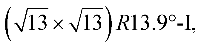
 and
and  .
.
| Structure name | Ag reconstruction | Si reconstruction | Mismatch | Angle (°) |
|---|---|---|---|---|
| (4 × 4) or H | (4 × 4) | (3 × 3) | 1.011 | 0 |
|

|

|
0.993 | 10.89 |
|

|
|
1.033 | 26.99 |
|
|

|
1.033 | 5.21 |
The first one is associated with a (3 × 3) reconstructed silicene lattice, whereas the others with a  reconstructed silicene lattice. Type I and type II
  reconstructions differ by the angle between the silicene and Ag lattices (27° or 5.2°, respectively). In some papers, these phases are respectively labelled as
  and
and  . Note that the
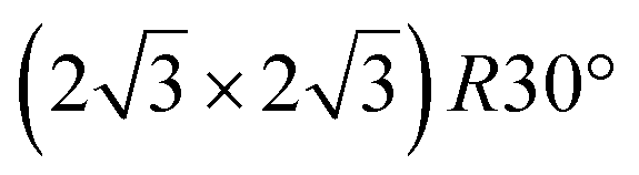
  reconstruction has been also identified as a “T-phase”,8 “dotted phase”54 or (3.5 × 3.5)R26° reconstruction.55 The conclusions of these detailed studies are that the
  structure forms at high growth temperature (T > 500 K), whereas
  and (4 × 4) structures form at lower temperatures. The dotted phase appears to form at low coverage and temperature. The earlier works concerning the growth conditions for the different phases are well summarized in ref. 56.
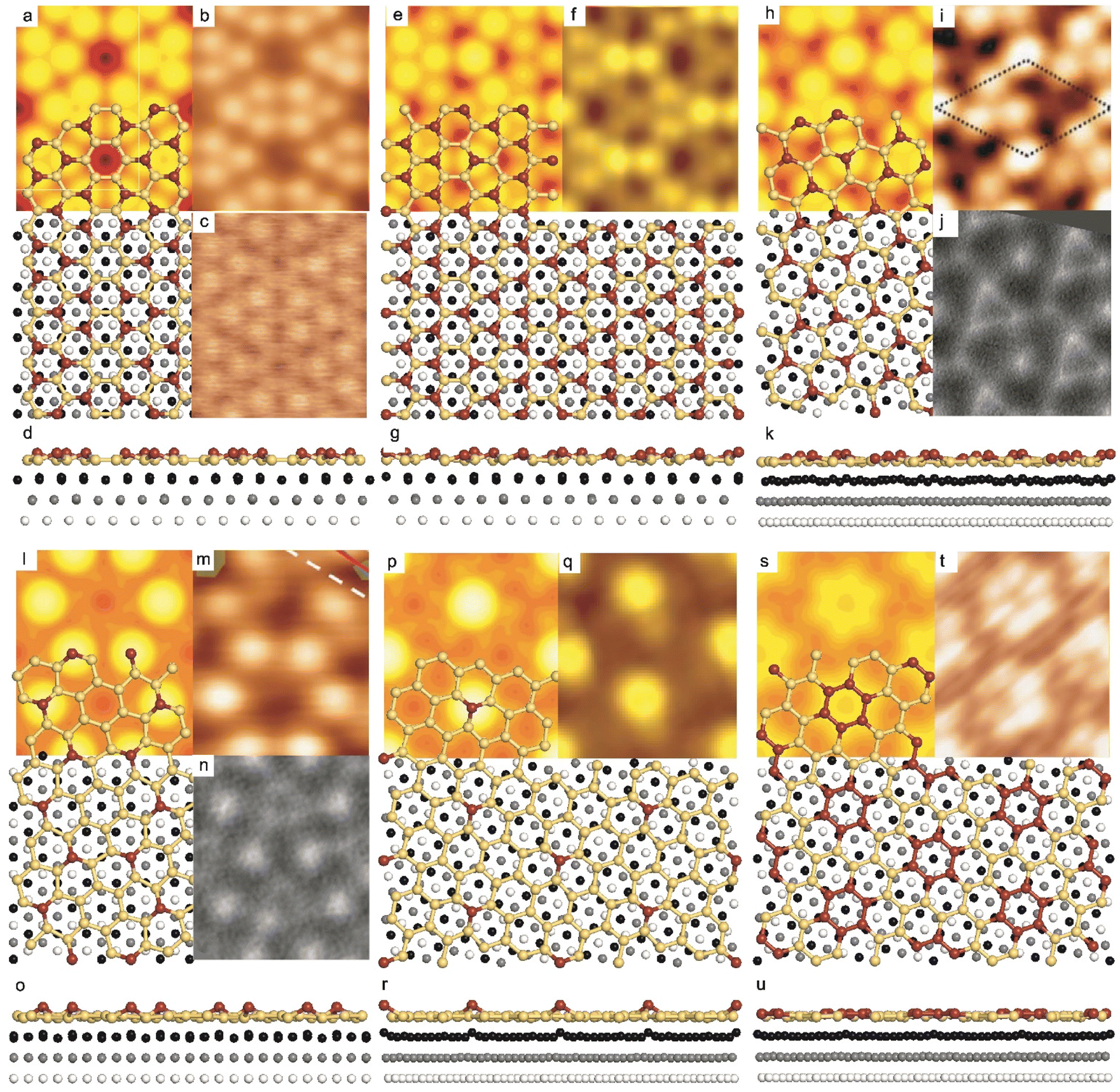 | ||
Fig. 1 Atomic models of silicene/Ag(111) reconstructions (d, g, k, o, r, u) and simulated STM images (a, e, h, l, p, s) adapted from ref. 33. Corresponding experimental STM (b46, f47, i48, m49, q47) and AFM (c50, j51, n51, t52) images. (a–g) (4 × 4) reconstruction. (h–k)  -type II reconstruction. (l–o) -type II reconstruction. (l–o)  reconstruction. (p–u) reconstruction. (p–u)  -type I reconstruction. Adapted with permission from ref. 33, 50 and 52, Copyright 2019 and 2017 by the American Physical Society, with permission of IOP Publishing, Ltd, from ref. 46 and 49, Copyright 2016 and 2015, with permission from Elsevier, from ref. 48, Copyright 2014 and with permission from ref. 47 and 51. -type I reconstruction. Adapted with permission from ref. 33, 50 and 52, Copyright 2019 and 2017 by the American Physical Society, with permission of IOP Publishing, Ltd, from ref. 46 and 49, Copyright 2016 and 2015, with permission from Elsevier, from ref. 48, Copyright 2014 and with permission from ref. 47 and 51. | ||
In addition to this (4 × 4) structure, another (4 × 4) reconstruction has also been identified by STM.47,56,66,70 It corresponds to a shift of the previous unit cell with respect to the Ag lattice by 1/3 or 2/3 of the Ag unit cell along the diagonal (Fig. 1e–g). It forms only small domains at the boundary between domains of (4 × 4) that are shifted by one Ag unit cell. Indeed, it has been shown that among all possibilities of superimposing the Ag and silicene lattices, only three of them do not break the p3 symmetry of the system.33 Indeed, the model of Vogt et al. is the most stable one, with an adsorption energy Eads = 0.144 eV per atom (with respect to bulk Si), whereas the two others have slightly higher adsorption energies (Eads = 0.145 eV per atom and Eads = 0.146 eV per atom). These positive adsorption energies imply that the system is metastable with respect to the formation of large Si crystallites. Simulated STM images of these two configurations are in very good agreement with experimental observations (see Fig. 1e and f).33
 -type II reconstruction.
The
-type II reconstruction.
The  -type II reconstruction has been initially described as a (3 × 3) silicene reconstruction.9 It would have corresponded to a highly constrained layer, with a mismatch of 0.911. In this seminal model derived from DFT calculations, the silicene layer is regularly buckled with a vertical displacement of ∼1 Å, corresponding thus almost to the free-standing silicene configuration. However, a model of a
  reconstructed silicene lattice was soon proposed, associated with a smaller mismatch (1.033).10 DFT simulations have shown that it corresponds to a configuration where 4 (out of 14) silicon atoms occupy the highest plane, 2.9 Å above the silver surface, and the rest of the silicon atoms occupy a lower plane, 2.1 Å above the surface.60 The Si atom at the node of the unit cell is on top of a Ag atom (see Fig. 1h–k). Simulated STM images60 are in good agreement with experimental observations. Similar values of the buckling have been computed with DFT in the last ten years.48,61,63,71,72 In another DFT study, it was proposed that the node of the unit cell corresponds to a silicon ring, so that none of the Si atoms in the unit cell is on top of a Ag atom.73
As for the (4 × 4) structure, there are only three atomic configurations that do not break the p3 symmetry of the system. Two configurations corresponding to top Si atoms at the nodes of the unit cell have nearly similar adsorption energies: Eads = 0.150 eV at−1 and Eads = 0.152 eV at−1, whereas the third one is less stable with Eads = 0.201 eV at−1.33 Indeed, this corresponds to STM observations where two different domains are clearly visible.48,74 The presence of the two most stable configurations has been also confirmed by SXRD33 and AFM.51,75 The value of buckling determined from AFM measurements is 0.98 Å,51 while it corresponds to 0.71–0.74 Å from SXRD.
However, these simple models do not account for all the complexity of the silicene structure. Indeed, it has been observed that the layer is not strictly commensurate with the substrate. This leads to moiré-like patterns in STM images.47,71,76 A comprehensive study of the moiré pattern has been given by Jamgotchian et al.74 The moiré corresponds to a larger unit cell, namely 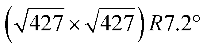 , corresponding to the matching between a silicene lattice of 0.384 nm and the silver substrate. This is in good agreement with LEED observations.74 SXRD experiments have indicated a slightly higher value of the average silicene lattice constant, 3.884 Å, with an angle between the silicene and silver lattice which varies with the growth temperature.33 From a microscopic point of view, the
 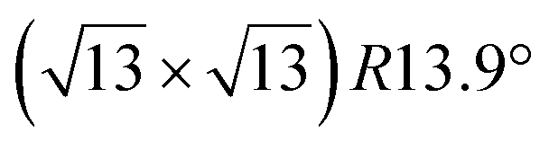 structure is not perfect but composed of a periodic arrangement of perfect and defective areas. In the model proposed by Jamgotchian et al., the perfect areas of silicene layers are slightly expanded due to a strain epitaxy, whereas the defective areas correspond to distorted Si rings.74 This model has been further confirmed by AFM measurements.51
 reconstruction.
The
reconstruction.
The  reconstruction has been initially observed by LEED.77 However, due to a misinterpretation of associated STM images, it was described at that time as a highly compressed silicene layer with Si–Si projected distances of 0.19 nm, i.e. much smaller than the 2.23 Å distance expected for free-standing silicene. In this initial work combining LEED and STM, an atomic model of a
  silicene reconstruction was proposed, which obviously could not match the observations. These contradictions were soon underlined.9,78 However, the existence of the
  reconstruction was confirmed in the combined STM and DFT study of Feng et al.8 and by other STM studies.10,54 The model of a
  silicene lattice was shown to be in good agreement with these new STM observations. In this model, 2 over 14 atoms of the unit cell are at on-top positions and are imaged by STM, while the other atoms are not seen (see Fig. 1l–o). DFT computations have indicated that the buckling of the layer is of the order of 1 Å to 1.53 Å.33,51,60,61,63,73 As for the other ordered structures, there are only three atomic configurations that do not break the p3 symmetry of the system, but the two other configurations, corresponding to no Si atom on top of Ag atoms have higher formation energies. The ground state model has been experimentally confirmed by SXRD and AFM.33,51
Similarly to the  -type II reconstruction, the
  reconstruction is not strictly commensurate with the substrate and presents a Moiré-like pattern.8 It has also been described as a defective silicene layer where domains of regular Si hexagons are separated by domain boundaries of deformed Si hexagons.79 It has been proposed that this layer was a patchwork of fragmented silicene pieces,80 but hydrogenation of the layer demonstrates that it is not the case and that the layer is a complete silicene sheet.81 The nature of the moiré in relation with the local atomic structure has been discussed by Jamgotchian et al. with a model of defects separating regular areas.49 The average silicene lattice constant in the layer was measured by SXRD. The value found, 3.884 Å, was the same as the one measured for the
  -type II reconstruction, with an angle between the two lattices of 10°, i.e., very close to the theoretical one (10.89°).33
It has been initially assigned to individual hexagon rings,8 or to a dense silicene sheet, corresponding to an ordered reconstruction. Protrusions would either correspond to six or three top lying Si atoms,8,10,54,83 or could be associated with one Si atom on top of a Ag substrate atom.47,60,84 On the basis of LEED and STM observations, the dotted phase has been assigned to a  -type I reconstruction,10,83 a
  reconstruction,54 or a (3.5 × 3.5)R26° unit cell with respect to the Ag(111) lattice.55 This corresponds to a unit cell size in the 0.76–1.04 nm range, reflecting the various sizes and angles experimentally measured.
Various models of  -type I reconstructions have been computed by DFT.60,71,72,84 All stable models correspond to a silicene lattice rotated by 26.99° with respect to the Ag lattice, and different registries have been proposed. From a thermodynamic point of view, the
  -type I reconstruction appears less stable than its
  -type II counterpart, where the silicene and substrate lattices are rotated by 5.21°.33,61 Among the different configurations that respect the p3 symmetry, the most stable one corresponds to Si atoms on top of Ag atoms at the node of the unit cell (see Fig. 1p–r). The adsorption energy per Si atom (Eads = 0.166 eV at−1) is 16 meV higher than for the most stable
  -type II configuration. On the contrary, the configuration corresponding to a Si hexagonal ring centered around a Ag surface atom at the node of the unit cell (see Fig. 1s–u) is much less stable, with Eads = 0.216 eV at−1.33
Micro-LEED experiments have confirmed the existence of silicene domains where the silicene lattice is indeed rotated by 27° with respect to the Ag lattice, in agreement with the model of a  silicene reconstruction.53 However, LEED I(V) curves are quite different from the ones obtained on the other well-ordered reconstructions, which could reflect a higher substrate-layer distance.53 The large width of the diffraction spots, also observed in LEED,10 reflects the poor ordering of the structure, visible in STM experiments. Such conclusion was also given in a tip-enhanced Raman spectroscopy (TERS) study.85 Indeed, the dotted phase has been described as a non-uniform structure having only short-range ordering.47 STM experiments performed at 480 K during Si growth showed that the dots are moving, whereas the
  -type II and (4 × 4) reconstructions are stable.82
A recent AFM study provided more structural information on the atomic structure of the dotted phase.52 In AFM, the dots visible in STM were clearly imaged as hexagonal rings (see Fig. 1t). These rings correspond to upper buckled Si atoms of a silicene plane. Two orientations have been found for this silicene plane, either 27° (corresponding thus to a  -type I reconstruction) or 30°, associated with a tiling pattern. There is thus a contradiction with DFT simulations showing that such configurations should be less stable than those with Si atoms on top of Ag atoms.
 reconstruction corresponding to a stoichiometric surface alloy has thus been proposed,89 but never confirmed. Disordered areas that appear at the beginning of the growth could also be surface alloys.82 From recent AFM measurements, it was on the contrary concluded that the disordered areas that appear at the domain boundaries of the well-ordered reconstructions, forming dark areas in STM images, are pure silicene phases. Indeed, AFM imaging of these dark regions revealed the signature of multiple structural motifs forming a “glassy-like” silicene region where buckled hexagons, pentagons, and heptagons appear interconnected.51 However, as the AFM technique is not chemically sensitive, such observations cannot decide the question. Very recently, normal incidence X-ray standing wave experiments have been interpreted in the framework of a pervasive Si surface alloy, located beneath the 2D-Si layer.90
These earlier works give however a too simple description of the growth mechanisms. Indeed, it has been observed by STM that silicene domains grow by replacing Ag atoms from the substrate.86,92 These expelled Ag atoms condense at step edges or form new terraces (see Fig. 2).86 The kinetic energy barrier for Si insertion has been experimentally determined to 0.43 eV, on the basis of the thermal evolution of the nucleation rate of silicene.82 DFT simulations have indicated a value of 0.617 eV for insertion of the first Si atom, while this value is only 0.228 eV for inserting a second Si atom.87 These low energy barriers explain why Si insertion already occurs at room temperature (RT).86 A less good agreement was found concerning the diffusion barrier of silicon atoms on a Ag(111) surface. From the island density measured at low temperature, for which no insertion occurs, a value of 0.26 eV was found,82 whereas the values computed by DFT were only 0.031 eV in one study84 or 0.124 and 0.16 eV in two other studies.87,93 However, these values give a good description of the initial nucleation process. Incoming Si atoms diffuse by atomic jumps on the surface until they insert, leading to the nucleation and growth of inserted silicene domains.
 | ||
| Fig. 2 STM images (325 nm)2 of the evolution of the Ag(111) surface during Si evaporation at 440 K. (a) Bare surface. (b–d) For Si coverages of 0.09, 0.49 and 0.74 ML, respectively. Triangular domains correspond to inserted silicene islands, while outgrowths forming from the terraces correspond to Ag expelled atoms that recondense. Adapted from ref. 86, with permission of AIP Publishing. | ||
The evolution with temperature of the density of such silicene domains is shown in Fig. 3a. The observed behavior with a “Λ shape” is far from the prediction of the classical theory, and is explained by the transition between a low temperature regime where Si atoms do not insert in the surface and diffuse with a low energy barrier by atomic jumps, to a regime where atoms diffuse by jumps and exchange with Ag atoms.82
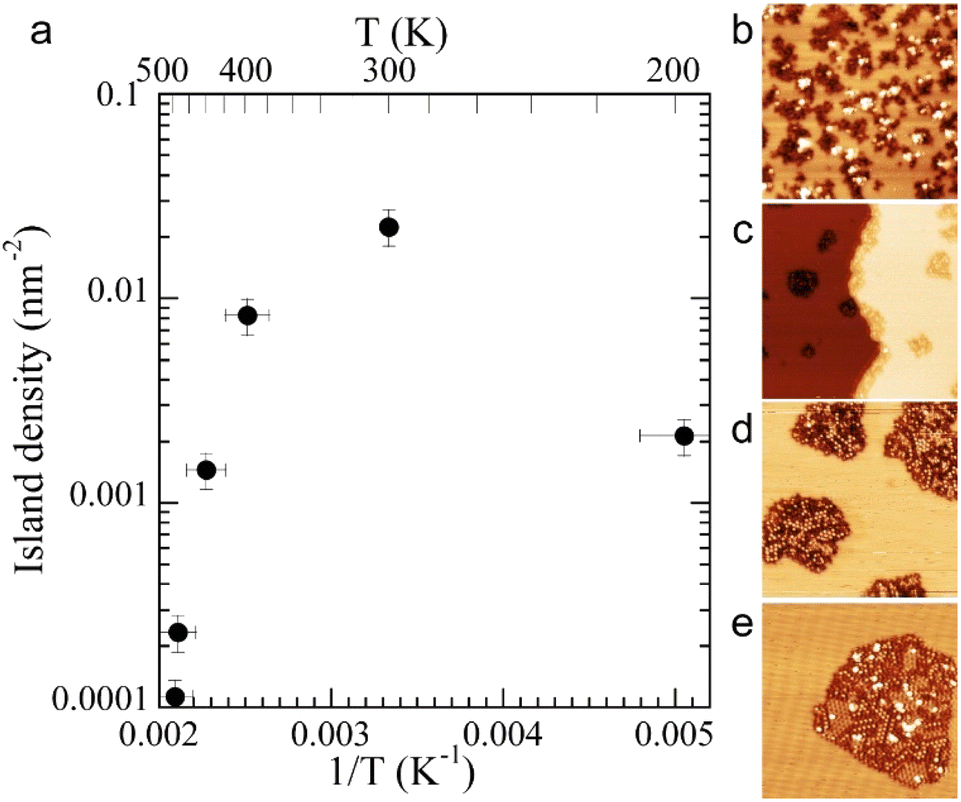 | ||
| Fig. 3 (a) Evolution of the density of silicene islands grown on Ag(111) as a function of the inverse of the growth temperature. (b–e) Morphology of small Si domains for growth at 300, 400, 440 and 480 K, respectively. Size of the images: 43 × 43 nm2. Adapted with permission from ref. 82, Copyright 2015 by the American Physical Society. | ||
The growth of these domains has been observed in situ in real time by STM.82 Si atoms incorporate initially at step edges, leading to step edge faceting. Silicene domains grow thus preferentially from the step edges, forming stripes,94 but silicene islands were also observed on the terraces, in particular at low temperature for which the diffusion length is smaller. Small silicene islands or narrow stripes are disordered. Ordered silicene domains, corresponding to the different phases described above, start to form for a growth temperature higher than 400 K and sizes above 10 nm as illustrated in Fig. 3b–e.82 Disordered regions can be considered as precursor for the nucleation of ordered silicene regions. They are progressively replaced by ordered ones with increasing coverage, showing the high mobility of Si atoms at such temperatures. The dotted phase is also replaced by more stable phases, namely the (4 × 4) and  -type II reconstructions, in agreement with LEED observations.53
Some DFT computations have been devoted to the formation and diffusion of point defects. Si adatoms and vacancies diffuse very fast, which could explain the formation of a well-ordered silicene layer above 500 K.95
For a Si chemical potential equal to the one of Si bulk, all DFT computations have indicated that the silicene layer has a positive formation energy.33,61 Silicene/Ag(111) is thus metastable with respect to formation of large Si clusters. This has been observed by LEEM.97 Submonolayer Si deposits annealed above 630 K showed dewetting. Moreover, if growth is performed above 540 K, it is not possible to fully cover the substrate with silicene,8 and dewetting is observed above a critical coverage.53,80,97 Very recently, kinetic Monte-Carlo (KMC) simulations of the dewetting have been performed. They revealed that the differences in the activation energies of diffusion on bare Ag, monolayer silicene and bulk Si were essential in the dewetting process.98
3.2 Si on Ag(110)
Si/Ag(110) was the first system studied that suggested that silicene could be synthesized through epitaxial growth on an atomically well-defined substrate. This system has generated a lot of interest since the reported presence, in 2010, of electronic dispersion similar to the one of graphene in ARPES spectra associated with the growth of 1D Si nanostructures and the prediction that such nanostructures possess a honeycomb-like structure.99Single and double Si nanoribbons. In 2005, Leandri et al. were the first to report that upon submonolayer deposition of Si onto the anisotropic silver (110) surface, flat lying Si nanowires with a high aspect ratio develop spontaneously at RT.100 STM and LEED revealed that these grown nanostructures, varying only in length, have a same characteristic width of 16 Å and are perfectly aligned along the atomic troughs of the bare surface, i.e. running along the [1
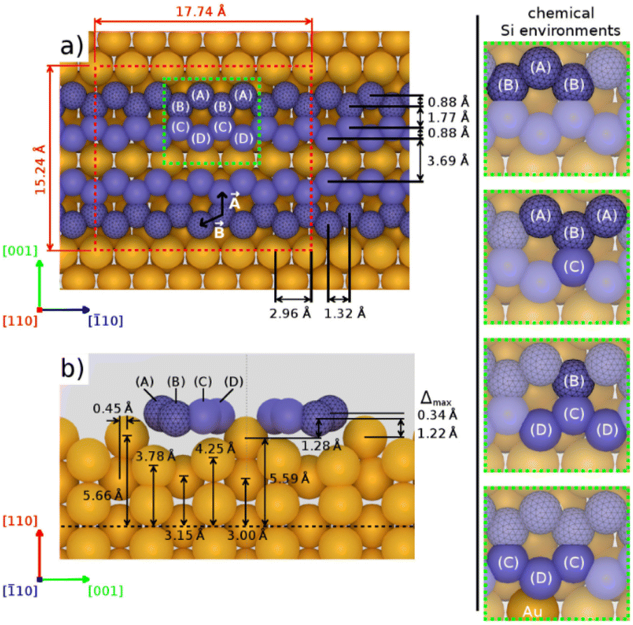
![[1 with combining macron]](https://www.rsc.org/images/entities/char_0031_0304.gif) 0] direction with a ×2 periodicity along their edges. Theses nanowires are ultrathin with an apparent height measured by STM less than 0.2 nm. Photoelectron spectroscopy (PES) revealed the existence of just two non-equivalent silicon environments. In 2007, based on STM and LEED investigations, Sahaf et al. showed that upon Si deposition at ∼470 K, the Si nanowires self-assemble by lateral compaction in the [001] direction to form an ultrahigh density array of identical nanowires (pitch of ∼2 nm).101 At completion, this 1D superlattice with (5 × 2) periodicity uniformly covers the entire substrate with a remarkably high degree of structural order. It was later shown, using high-resolution STM, that the nanostructures grown at RT and 470 K, named nanoribbons (NRs),102 differ only by a factor 2 in their width, with a width of 0.8 and 1.6 nm, respectively.103 In STM images, the narrowest and largest NRs appear commonly as composed of two and four rows of round protrusions and will be denoted hereafter single NRs (SNRs) and double NRs (DNRs), respectively (see Fig. 4a and b). The growth of SNRs and DNRs was studied in details using STM and surface diffraction techniques (LEED and SXRD) by Colonna et al. and Bernard et al. in 2013.104,105 The Si deposition temperature was demonstrated to be a key parameter to control the width of the Si NRs formed. At RT, most of the grown NRs are SNRs randomly distributed on silver terraces, while few of them are DNRs. As the substrate temperature increases, the ratio between DNRs and SNRs increases and at 460 K, essentially DNRs form upon Si deposition, arranged in an extended (5 × 2)/c(10 × 2) superstructure (called (5 × 2) superstructure in the following). The (5 × 2) superstructure was found to be stable until 490 K, temperature above which a silver surface faceting induced by Si adatoms occurs.106,107
0] direction with a ×2 periodicity along their edges. Theses nanowires are ultrathin with an apparent height measured by STM less than 0.2 nm. Photoelectron spectroscopy (PES) revealed the existence of just two non-equivalent silicon environments. In 2007, based on STM and LEED investigations, Sahaf et al. showed that upon Si deposition at ∼470 K, the Si nanowires self-assemble by lateral compaction in the [001] direction to form an ultrahigh density array of identical nanowires (pitch of ∼2 nm).101 At completion, this 1D superlattice with (5 × 2) periodicity uniformly covers the entire substrate with a remarkably high degree of structural order. It was later shown, using high-resolution STM, that the nanostructures grown at RT and 470 K, named nanoribbons (NRs),102 differ only by a factor 2 in their width, with a width of 0.8 and 1.6 nm, respectively.103 In STM images, the narrowest and largest NRs appear commonly as composed of two and four rows of round protrusions and will be denoted hereafter single NRs (SNRs) and double NRs (DNRs), respectively (see Fig. 4a and b). The growth of SNRs and DNRs was studied in details using STM and surface diffraction techniques (LEED and SXRD) by Colonna et al. and Bernard et al. in 2013.104,105 The Si deposition temperature was demonstrated to be a key parameter to control the width of the Si NRs formed. At RT, most of the grown NRs are SNRs randomly distributed on silver terraces, while few of them are DNRs. As the substrate temperature increases, the ratio between DNRs and SNRs increases and at 460 K, essentially DNRs form upon Si deposition, arranged in an extended (5 × 2)/c(10 × 2) superstructure (called (5 × 2) superstructure in the following). The (5 × 2) superstructure was found to be stable until 490 K, temperature above which a silver surface faceting induced by Si adatoms occurs.106,107
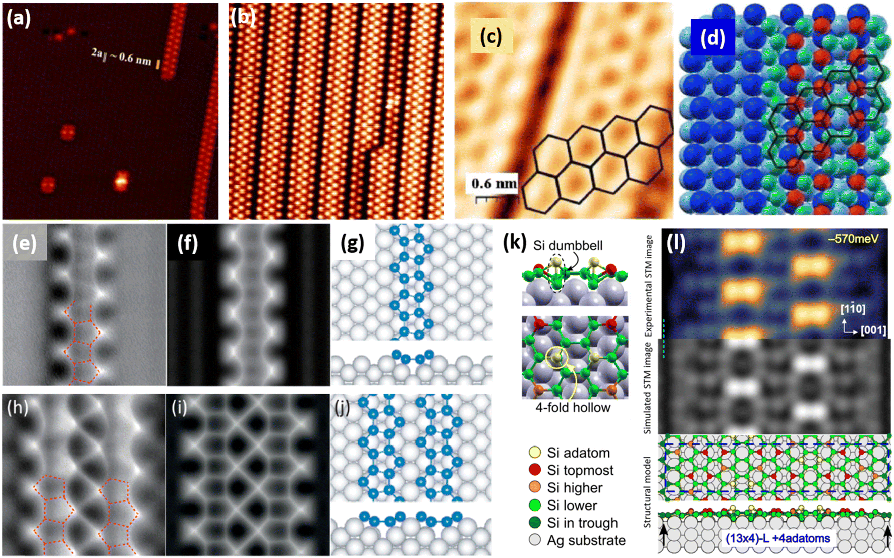 | ||
| Fig. 4 1D and 2D Si structures on Ag(110). (a) STM image (15 nm)2 of Si SNRs upon Si deposition at RT. Nanoclusters, later assigned to precursor structures of Si SNRs, are also observed.115,116 (b) STM image (15 nm)2 of self-assembled Si DNRs grown on Ag(110) upon Si deposition at 470 K, forming a (5 × 2)/c(10 × 2) superstructure. Occasionally, some SNRs are also formed. (c and d) STM image of Si NRs with few honeycombs drawn and ball model of the calculated honeycomb structure. Top most Si atoms are represented by red balls and other Si atoms by green balls. (e and f) Experimental and simulated AFM images of Si SNR, respectively. Pentagonal rings are visualized, as outlined by red dash lines drawn. (h and i) Experimental and simulated AFM images of Si DNR, respectively. (g and j) Top and side views of the pentamer structure for Si SNR and Si DNR grown on the MR reconstructed Ag(110) surface, respectively, as proposed by Cerdá et al.115 Si atoms are denoted as blue spheres. (k) Local adatom geometry showing DB pair formation at 4-fold hollow site. (l) Experimental (blue-yellow colormap, top) and simulated (greyscale, center) STM images and the corresponding structural model of DB silicene (bottom). Adapted with permission from ref. 23 and 116, Copyright 2021 and 2018 American Chemical Society, with permission of John Wiley and Sons, from ref. 103, Copyright 2010 WILEY-VCH and with permission of AIP Publishing, from ref. 109. | ||
Honeycomb models. Elucidating the atomic structure of Si NRs has given rise to a long debate. Several one-atom thick structural models have been proposed in the literature over a decade. The first models were based on the assumption that the underlying Ag(110) substrate was not structurally modified, except for the relaxation of the first atomic layers. These models were essentially based on DFT calculations and STM imaging of the Si NRs. In 2006, Guo-min He proposed a model for the Si NRs where the energetically most favorable atomic arrangements identified are two Si dimer structures, almost degenerate in energy, very similar to that of a Si(100)2 × 1 surface.108 These geometries correspond to a layer of silicon atoms located in hollow sites of the silver substrate, which represents a continuation of the bulk stacking sequence, and a layer of Si dimer rows above. In the following years, a series of articles claimed that the Si NRs possess a honeycomb structure, eventually buckled, and thus correspond to silicene NRs.109–113 A detailed description of these models can be found in a review published in 2016 by Aufray and co-workers.114 These models echoed the reported graphene-like electronic signature measured by ARPES and attributed to the silicene character of the Si NRs grown on Ag(110).99 This point is discussed in Section 6.3. The first honeycomb structure was proposed in 2010 by Kara, Aufray and co-workers using DFT-based calculations (see Fig. 4c and d). In this model, 30 silicon atoms in a (6 × 4) unit cell on the Ag(110) surface relax into a honeycomb-like structure arched on the substrate.109,110 It was claimed that a honeycomb pattern on top of the silver substrate is clearly observed by STM, assigning the rows of protrusions observed to hexagons arranged in a honeycomb structure. It has to be noted that the honeycomb model proposed does not match the ×2 periodicity along the Si NR edges previously reported by LEED.100,101 Like this model, none of the honeycomb-based models proposed in the literature provide a satisfactory comparison with the experimental data.
Missing-row reconstruction of Ag(110). Using SXRD, Bernard et al. demonstrated that the Ag(110) surface undergoes a missing-row (MR) reconstruction underneath the Si NRs during the growth of both SNRs and DNRs, with two Ag MRs within a (5 × 2) unit cell.105 As observed for Si/Ag(111), expelled Ag atoms are incorporated at step edges or form new Ag(110) terraces. At that time, this result was quite surprising since (i) Ag and Si are known to form an abrupt interface and bare Ag(110) does not show any reconstruction under UHV and (ii) first models proposed for the atomic structure of NRs were based on the assumption that the underlying Ag(110) substrate was unreconstructed. Considering this decisive finding, two models were later proposed for the precursor structure of Si SNRs, observed in Fig. 4a: one has a quasi-hexagonal geometry and the other corresponds to two Si pentagons sitting side by side, both structures are located in an silver di-vacancy.115,116 A transition from cluster precursors to SNRs occurs when more Ag atoms are removed underneath a cluster to form a trough. In 2018, Daher Mansour et al. gave a deeper insight in the growth mechanisms of Si NRs on Ag(110).106 Their nanoscale investigation by means of STM for substrate temperature ranging from 300 K to 500 K showed the formation of local (3 × 2) superstructures composed of SNRs between 390 and 440 K and extended (5 × 2) superstructures above 440 K. This study outlines the role played by the MR reconstruction of the Ag(110) surface in the formation of extended Si NR arrays.
Pentamer structure. After the experimental demonstration in 2013 of Ag(110) MR reconstruction induced by the growth of Si NRs,105 several structural models, taking into account the possibility of a reconstructed substrate, were considered. An extensive work was proposed in 2015 by Hogan et al., where a range of Si NR structural models were investigated by means of total-energy calculations within DFT.117 One model has been found to be thermodynamically stable and in excellent agreement with experiment. It consists in a double zigzag chain of Si adatoms backbonded to Si dimers lying within the Ag MRs. The authors pointed out that their work provided clear evidence for a strongly bound Si–Ag reconstruction on Ag(110) and did not find any support for silicene-based models. Indeed, neither Raman spectroscopy nor surface differential reflectance spectroscopy (SDRS) identified spectral features which could be attributed to silicene-like layers adsorbed on the Ag(110) surface.118,119 In 2016, Cerdá et al. proposed an original Si pentamer chain model based on DFT calculations and STM image simulations.115 In this model, SNRs correspond to Si pentamer chains running along the MR troughs of the reconstructed Ag(110) surface with a rather large buckling of 0.7 Å (see Fig. 4g). As shown in Fig. 4j, DNRs correspond to twin Si pentamer chains arranged in a (5 × 2) superstructure with a Si coverage of 1.2 monolayer (ML) in silver (110) surface atom density, in fairly good agreement with the reported experimental value (∼8 ± 2 Si atoms per (5 × 2) unit cell).105,117 This atomistic model was rapidly confirmed by Prévot et al. by combining SXRD measurements to STM imaging and DFT calculations.22 In this study, the authors have screened several models published in the literature according to three independent criteria: STM imaging, DFT formation energies and SXRD experiments. The pentamer model was found to yield the best agreement across all criteria. The pentamer chain structure was later confirmed by a combined AFM-TERS study reported by Sheng et al. (see Fig. 4e, f, h and i) and by other investigations using various experimental techniques: X-ray photoelectron spectroscopy (XPS), X-ray photoelectron diffraction (XPD), reflectance anisotropy spectroscopy (RAS) and SDRS.116,120,121 All these studies have contributed to close the long-debated atomic structure of the Si NRs grown on Ag(110) and definitively excluded a honeycomb structure similar to that of free-standing silicene.
3.3 Si on Ag(001)
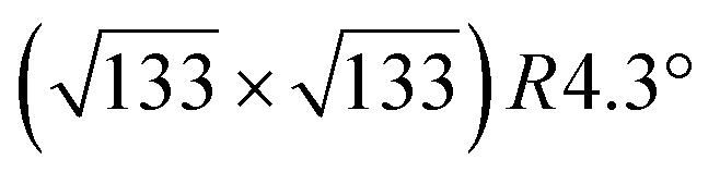
Although Ag(001) was the first silver substrate used to deposit Si at low coverage,124 this face has been less studied than (111) and (110) faces to grow low dimensional Si structures. It was reported in 2007 that Si deposition at ∼500 K leads to the formation of a (3 × 3) structure which evolves toward a more complex superstructure with increasing the coverage.34 Combining STM imaging and SXRD, a model with a Si coverage of 4/9 ML (where 1 ML corresponds to the Ag(001) atomic density) was proposed for the (3 × 3) reconstruction, consisting in 1D stripes of two tilted Si dimers per unit cell, with Si–Si interatomic distance corresponding to bulk Si. By increasing the Si coverage to 1.6 ML, a complex superstructure composed of stripes running along the [110] and [10] directions of Ag(001) appeared, forming two equivalent perpendicular domains and exhibiting locally a (7 × 4) reconstruction, as shown in Fig. 5a. A tentative model was proposed by the authors, consisting in a graphite-like silicon layer, i.e. a silicene layer (see Fig. 5b). Along the long (short) side of the rectangular unit cell, the silicene lattice has a lattice constant of 3.89 Å (3.85 Å).
 | ||
| Fig. 5 (a) STM image (6.4 nm)2 showing the complex superstructure grown on Ag(001) at 500 K. The local (7 × 4) unit cell is represented by the grey rectangle. The stripes are described by two joined chains of hexagons, drawn in black. (b) Tentative atomic model for the complex superstructure, consisting in a graphite-like silicon layer, i.e. a silicene layer. The black pattern, where black balls represent Si atoms sitting on top of silver atoms, shows the two joined hexagon structure observed in STM images. Adapted from ref. 34, Copyright 2007, with permission from Elsevier. | ||
Guo-min He, on the basis of DFT calculations, showed that the dimer model for the (3 × 3) reconstruction was unstable, and proposed alternative models.125 However, in a combined ARPES-DFT study, Geng et al.126 recently proposed a model composed of Si dimers, analogous to that proposed by Léandri et al.34 where the dimers are not tilted and the topmost Ag layer is reconstructed with missing Ag atoms. Guo-min He also proposed models for higher coverage structures, but they are associated with substrate reconstructions different than the (7 × 4) experimentally observed. Interestingly, for a Si coverage of 4/3 ML, a graphite-like Si layer with a c(6 × 4) structure (in fact a 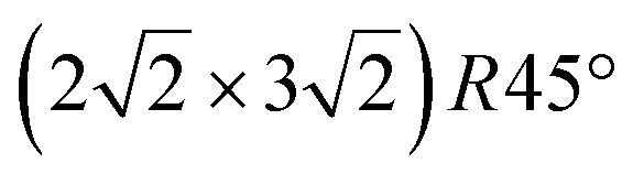 reconstruction) was found to be the most stable structure. Increasing the coverage, Si adatoms were found to adsorb at top sites of the lower atoms of the Si layer, i.e. in a DB configuration.
As a conclusion, further investigations are required to elucidate the atomic structure of low dimensional Si structures grown on Ag(001).
4. Silicene on other substrates
After the initial observations of silicene growth on silver, various other substrates have been tested for the synthesis of epitaxial silicene: monoelemental metals, lamellar substrates, refractory ceramics or insulating substrates.4.1 Silicene on monoelemental metal substrates
Among the variety of substrates used for silicene growth, many of them are metal substrates, in particular Al and Pb for which the equilibrium bulk phase diagram indicates phase separation with Si, contrary to Ir and Ru for which silicides form. The Au–Si system is more complex as various metastable silicide phases are known to form.First experiments on Au(100) concluded to the formation of Si clusters for RT deposition and low coverages (θ = 0.2 ML), whereas surface silicene formation was observed after annealing at 423 K.128 On the contrary, STM experiments performed on Au(111) showed that in the initial stage of deposition, Si atoms insert in the Au surface and expel Au atoms that condense at step edges.129 Annealing of 0.4 ML Si deposits lead to the formation of various striped patterns attributed to Au–Si alloys. Finally, STM observations of Si growth on Au(110) in the 633–773 K temperature range also concluded to the formation of an ordered surface gold silicide for low coverage deposition (θ = 0.2 ML).130 The surface presents a  reconstruction for which a model has been recently proposed on the basis of XPD results.131
These systems have been revisited in light of possible formation of silicene. On Au(110), STM observations showed that 0.3 ML Si deposition at 673 K leads to the formation of NRs of width equal to 1.6 nm.38 From an analogy with the structure of similar NRs grown on Ag(110), that was, at that time, supposed to be silicene, it was thus concluded that Si/Au(110) NRs are also silicene NRs. More recently, a model consisting of two rows of Si hexagons on a MR reconstructed Au(110) surface has been proposed for these NRs, on the basis of XPD measurements (see Fig. 6).132
 | ||
| Fig. 6 Structural model for the silicon NRs on Au(110) proposed from the fit of XPD data in top view (a) and side view (b). Reprinted from ref. 132, Copyright 2019, with permission from Elsevier. | ||
In 2017, a combined STM, LEED and ARPES study revisited the growth of Si on the Au(111) surface. After growth at 633 K, two ordered structures were observed by LEED: a faint (12 × 12) reconstruction and a reconstruction with rectangular unit cell (0.73 × 0.92 nm). Only this last structure was visible in STM images, while ARPES measurements suggested a “by-12” superstructure of silicene.133 While it is difficult to conclude on the structure of the (12 × 12) reconstruction in absence of any STM image, it must be underlined that the rectangular unit cell found by LEED and STM is the same as one of the reconstructions previously found by Shpyrko et al. at the surface of the eutectic liquid Au82Si18 and shown to be an alloyed surface structure.134,135
Completely different structures were observed by LEED after deposition of 1 ML of Si at 533 K.37 Two monoclinic unit cells were attributed to surface silicide, from the comparison with the results of Shpyrko et al.135 In addition to these structures, a rectangular unit cell (4.141 × 7.101 Å) was also found. It was associated with specific Raman peaks, and since it could not be associated with any known gold silicide phase, it was described as a highly (>7%) biaxially strained silicene phase, slightly deformed along one direction.37
It is interesting to compare these results to those obtained by Stępniak-Dybala et al.20 After Si segregation through a thin Au(111)/Si(111) epitaxial film, two ordered superstructures were observed by STM: a (0.75 × 0.94 nm) rectangular unit cell, very similar to the observations of Sadeddine et al.133 and a disordered hexagonal structure resembling the  silicene/Ag(111) reconstruction. The rectangular unit cell was associated with a surface alloy, while the hexagonal structure was assigned to planar silicene, with an average lattice constant of 4.1 Å, which is 6% higher than the expected value for free-standing silicene. Very recently, a LEEM/LEED study also identified another hexagonal phase after Si segregation at 473 K. It was assumed to be a Si bilayer, obtained by twisting two silicene layers with lattice constants of 3.85 Å and 4.34 Å.36 The growth of the silicene layer was followed in situ by LEEM.136 Annealing in the 420–535 K temperature range leads to the formation of hexagonal phases with a different lattice constant a0, which were assumed to correspond to low-buckled silicene layer (a0 = 3.85 Å), and planar silicene (a0 = 4.34 Å) developing above the low-buckled phase and separated from it by sparsely distributed Au atoms. Dewetting of the Au film occurs for annealing above 540 K.136
Thus, the Si/Au(111) system is extremely complex, due to the presence of numerous metastable bulk silicide phases. Quantitative structural characterizations are thus needed to determine the exact nature of the ordered phases observed.
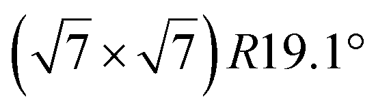
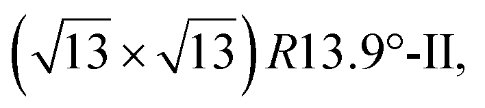
 structure was observed by LEED and STM.16 A model of buckled silicene, with a lattice constant of 4.15 Å, was proposed for this structure, corresponding to a (√3 × √3) silicene reconstruction. The stable configuration computed by DFT has one silicon atom on top of an iridium atom; two atoms at hollow sites and the other three atoms are located at the bridge sites (see Fig. 7).16 The kinetics of formation of the silicene layer has been studied by molecular dynamics (MD) simulations, showing the formation of highly defective honeycomb lattices.137 Note that in these simulations, impinging atoms are always adsorbed on Si-free regions, which strongly reduces the possibility of forming Si clusters instead of a wetting silicene layer.
 | ||
Fig. 7 Experimental (a) and simulated (b) STM images of the silicene/Ir(111) system. (c) Top view of the relaxed atomic model of the  silicene/ silicene/ Ir(111) configuration. Adapted with permission from ref. 16, Copyright 2013 American Chemical Society. Ir(111) configuration. Adapted with permission from ref. 16, Copyright 2013 American Chemical Society. | ||
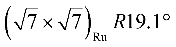
Concerning the structure of silicene/Ir(111), opposite conclusions have been drawn from a XPS study.138 Si was grown at various deposition temperatures or at RT followed by annealing. The only ordered structure found was a  one, formed at coverage below 0.5 ML. The different components in the corresponding Si 2p spectra have been assigned to Si atoms at hollow sites and Si atoms incorporated in the Ir surface. For higher coverage, namely above 0.5 ML, iridium silicide formation has been observed.138 Recently, it has been proposed that annealing of thin Ir/Si(111) at 1023 K leads to the formation of IrSi3 nanocrystals.41 Some of the crystallites present a hexagonal reconstruction (with size 23.1 Å) attributed to a
  reconstruction of silicene.41 However the lattice constant deduced (4.37 Å) is far from the one of free-standing silicene.
 reconstruction of the substrate for which a model of
  silicene reconstruction has been proposed and relaxed by DFT. This gives a lattice constant of 4.13 Å and a large buckling of 1.26 Å. However, in the LEED diagram shown, the (1 × 1) spots of silicene are not very intense with respect to the other diffraction spots, contrary to what was observed for example for Si/Ag(111), which may reflect a more complex structure.
In another study, silicene has been obtained by intercalation below epitaxial bilayer graphene (BLG), after annealing of a Si/BLG/Ru(0001) deposit at 900 K. The same  reconstruction was observed. Moreover, it was concluded from Raman measurements that the interfacial silicene decouples the BLG from the Ru substrate.140
4.2 Silicene on lamellar substrates
In order to better decouple the silicene layer from the substrate, attempts have been made to grow silicene by evaporation on a lamellar substrate. The objective of these studies was to obtain a silicene layer coupled to the substrate through weak van der Waals interactions. reconstruction attributed to the honeycomb lattice of silicene, with a lattice constant of 4.1 Å.39 Raman observations evidenced the presence of a new peak at 542.5 cm−1, associated with the strain and finite size of the silicene nanosheet.142 Moreover, it was observed that the silicene layer was stable in air.142 From a thermodynamical point of view, various atomic configurations of silicene sheets on graphene have been computed by DFT. Multiple phases of single crystalline silicene with different orientations should coexist at RT. Most stable configurations correspond to (4 × 4) silicene/
 graphene and
  silicene/
 graphene reconstructions. These nearly unstrained layers have silicene lattice constants of respectively 3.82 Å and 3.87 Å.143 In order to solve the apparent contradiction with experimental results that indicate the formation of a single phase with higher strain, DFT calculations for small silicene islands have been undertaken.144 It appears that for islands below a size of 50 atoms, the
 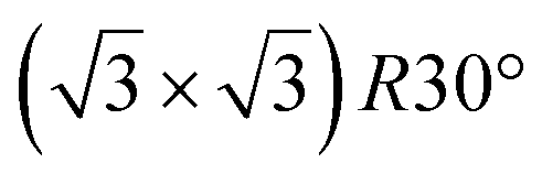 reconstruction is more stable than the
  one. Ab initio molecular dynamics (AIMD) simulations showed that the incoming flux of Si atoms could prevent the 2D islands to convert into 3D islands. However the needed flux is orders of magnitude higher than the experimental one.144
A simple explanation has been however given. It was shown that the observed apparent  reconstruction is caused by charge density modulations in the HOPG surface at the vicinity of the 3D Si clusters. Indeed, the transition between
  and (1 × 1) is very smooth, in contradiction with a sharp transition due to the edge of a 2D island, but in very good agreement with the attenuation length of a charge density wave.145 As for MoS2, it was also proposed that part of the Si is intercalated between graphite layers.146 Such RT intercalation would occur at the defects of the graphite surface.
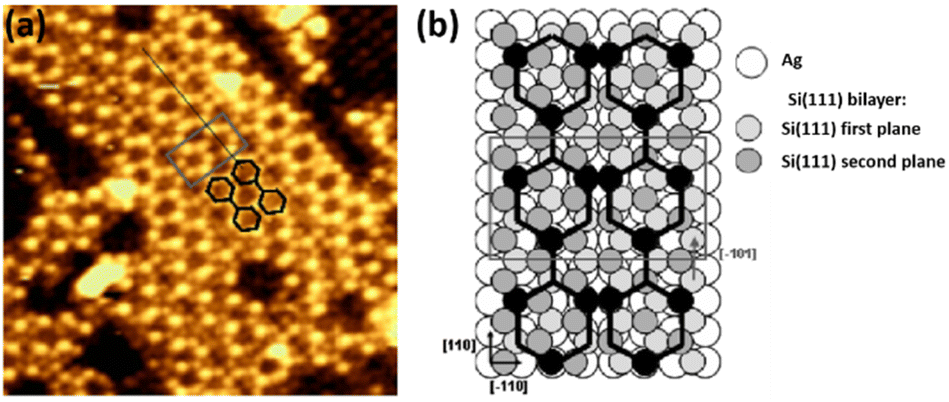
In another study, evaporation of Si on a substrate held in the 1023–1073 K temperature range was shown to lead to the formation of Si thick islands and silicene domains with a lattice constant of 3.53 Å, as shown by STM images.40
4.3 Silicene on refractory ceramics
The growth of silicene has been reported on two metallic refractory ceramics: ZrB2 and ZrC that were recognized as highly stable substrates for crystal growth.![[2 with combining macron]](https://www.rsc.org/images/entities/char_0032_0304.gif) 0〉 directions with a local (2 × 2) reconstruction, attributed to a
0〉 directions with a local (2 × 2) reconstruction, attributed to a  reconstructed silicene with a lattice constant equal to 3.65 Å. From XPS measurements, three Si components were observed. A model of “regularly buckled-like silicene” can be proposed for this local (2 × 2) structure. In this model, two Si atoms are on hollow sites of the Zr lattice, three Si atoms at the intermediate position between top and bridge sites, and one Si atom on the top of a Zr atom. The buckling of the layer is 0.91 Å.15 Energetically, this structure is not the ground state since a model of “planar-like silicene”, with only one atom being 1.59 Å above the others, is more stable (see Fig. 8).147 It was also proposed, from DFT calculations, that this phase was stabilized by line boundaries that miss on-top Si atoms. This allows the system to reduce both the atomic surface density and the total energy.44 This planar-like model has been invoked to explain ARPES148 and high-resolution electron energy loss spectroscopy (HREELS)149 measurements. First principle calculations of XPS spectra have further shown that the model reproduced indeed very well the experimental results.150
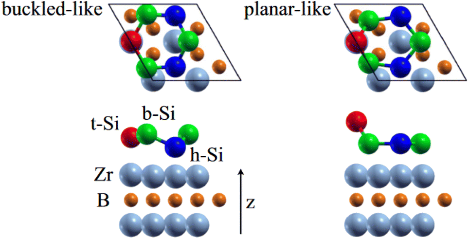 | ||
| Fig. 8 Structures of buckled-like and planar-like silicene, where the top Si (red), bridge Si (green), and hollow Si (blue) are indicated. Adapted with permission from ref. 150, Copyright 2017 by the American Physical Society. | ||
Experiments have shown that it was possible to remove the stripe pattern by adding 0.03–0.05 ML of Si at a temperature above 483 K, in spite of an increase of the total energy per Si atom.151 A mechanism for adatom integration into the initial stripe pattern has been proposed, based on STM measurements performed at RT after deposition of 0.015 ML of Si.152
 silicene reconstruction with a lattice constant of 3.84 Å. Phonon dispersion curves have been obtained from HREELS measurements. The calculated phonon dispersion agreed well with the experiment, even though not all the calculated modes were observed experimentally. Unfortunately, no other characterization of this system has been undertaken up to now.
4.4 Silicene on an insulating substrate: NaCl
In order to decouple the silicene layer from the metallic substrates often used for epitaxial growth, Si has been evaporated on thin NaCl/Ag(110) films hold at 413 K and annealed at 473 K.42 After 0.2 ML Si evaporation, darker areas appear in STM images, attributed to small 2D Si structures. For 1 ML deposition, the surface is completely covered and shows a (3 × 4) reconstruction with respect to the Ag substrate. STM images resemble the one obtained for silicene growth on Ag(110), but the size of the unit cell along the [10] direction is 0.86 nm instead of 1.16 nm. A model of Si NRs was proposed for this structure, in agreement with EXAFS measurements. As compared with a complete silicene sheet, this structure has dangling bonds that need to be stabilized by H atoms.42 However, it must also be underlined that the model should correspond to a larger (12 × 4) unit cell when taking into account the NaCl buffer layer. It would have been interesting to compare experimental and simulated STM images.
5. “Multilayer” silicene
Soon after the discovery of silicene, the question of forming stacks of silicene layers has been raised. Up to now, no evidence has been given of the existence of silicene layers interacting through van der Waals forces, such as graphene layers. However, a few systems obtained after deposition of two or more Si MLs (where 1 ML corresponds to the silicene atomic density) have been shown to possess a structure different from the one of bulk silicon.5.1 Thin silicon films/Ag(110)
The possible formation of multilayer silicene NRs has been raised after growth of Si/Ag(110) at high coverage.153 STM observations showed the formation of nm thick NRs, appearing as a stacking of several layers with an interlayer spacing of 2.9 Å. These NRs have a flat top layer with a (5 × 4) reconstruction with respect to the Ag(110) substrate. However, it has been later shown that these NRs were the result of silver faceting stabilized by silicon atoms. They thus consist of a silver core, with a Si-covered surface.1075.2 Thin silicon films/Ag(111)
Soon after the discovery of silicene on Ag(111), the structure and electronic properties of thicker films have been studied. It was initially observed by LEED and STM that after completion of the first silicene layer, another structure forms on the surface that shows a reconstruction with respect to a silicene plane, i.e. a
 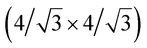 reconstruction with respect to the Ag(111) unit cell.8,55 Some authors claimed that it is another silicene phase,8,154,155 while other authors proposed that it corresponds to a second silicon layer.55 De Padova et al. indeed reported in 2013 the growth of thicker Si films on Ag(111).25,156 Such films were obtained by evaporating up to 10 ML of Si on Ag(111) held at 470 K. From LEED and STM measurements, it was observed that the
  reconstruction persists up to several layers of silicon coverage. From STM measurements, it was suggested that the
  reconstruction grows on top of the silicene (3 × 3)/Ag(111)(4 × 4)structure.157
The exact nature of such “multilayer” silicene has been for a long time controversial. Three theories have been raised for the structure observed: thick Si epitaxial films grown at 470 K would correspond to either a novel silicon allotrope or to diamond-like silicon terminated by a novel  reconstruction, or to diamond-like silicon terminated by the Ag/Si(111)
  reconstruction.
To support the theory of multilayer silicene, it was shown by X-ray diffraction (XRD) that both the interlayer spacing and surface lattice constant (3.090 Å and 6.477 Å, respectively) were smaller for multilayer silicene than for a Si crystal terminated by a Ag/Si(111) (√3 × √3) reconstruction (3.136 Å and 6.655 Å, respectively).158,159 The Raman spectra showed a peak at 523.3 cm−1 instead of 520.4 cm−1 for bulk Si.158
However, high-resolution STM images obtained after growth in the 450–550 K temperature range showed that the successive hexagonal layers display an ABC stacking, leading to the conclusion that they are diamond-like silicon.160 The pealing of the surface with a STM pulse, at liquid nitrogen temperature, revealed that underlying layers adopt the same  reconstruction, suggesting that this reconstruction is genuine, and not due to the presence of Ag.160 Various possible reconstructions of bare Si(111) surfaces have been computed by DFT.161
Eventually, the affirmation that Si deposition on Ag/Si(111) leads to the growth of diamond-like Si covered with Ag was first proposed from STM/scanning tunneling spectroscopy (STS) measurements,162 showing the similarity with the Ag/Si(111)  reconstruction, with an atomic model known as honeycomb-chain triangle (HCT). This hypothesis was confirmed by several independent groups, with numerous different experimental techniques such as LEED I(V),163,164 SXRD,165 (see Fig. 9), AES associated with differential reflectance spectroscopy,166 ARPES,167,168 metastable atom electron spectroscopy,169 or AFM.170 The presence of surfactant Ag atoms was also evidenced from STM observations after deuterium exposure.171 In addition, SXRD measurements evidenced the presence of numerous stacking faults for deposition at 520 K that could explain the difference of lattice constant observed with the one of bulk Si.165
 | ||
| Fig. 9 Maps of the intensity diffracted by 8 ML of Si evaporated on Ag(111) at 520 K growth. The h, k indices correspond to in-plane directions, whereas l corresponds to the out-of-plane direction. (a) Map for k = 0. (b) Map for h = k. The color scale is the same for both maps. The indexed spots belong to diamond-like silicon with four orientations (corresponding to blue, red, green and black labels). Reprinted with permission of IOP Publishing, Ltd, from ref. 165, Copyright 2017. | ||
The mechanisms of thin silicon films growth have been elucidated by in situ STM and DFT calculations.172 After completion of the silicene layer, the film grows by insertion of Si atoms below the silicene layer, instead of growing on top of the silicene layer. Two reconstructions were observed: the first one corresponds to a Si bilayer covered with Si adatoms while the second one is the Ag-covered honeycomb chained triangle (HCT) reconstruction. This last one is more stable and progressively covers the whole surface. KMC simulations have been used to model the growth of silicon layers at various temperatures. With a small set of parameters, simulations reproduce well the evolution of the surface observed by STM, LEED and AES.173
To conclude, although differences between Si thick films grown at low (300 K), intermediate (470–500 K) and high (620 K) temperatures have been reported,26 there is no structural evidence of a new silicon allotrope. The differences observed between layers grown at 473 K and bulk silicon may be explained by the presence of defects during growth such as stacking faults.
5.3 Thin silicon films/Si(111)
Multilayer silicene has also been claimed to grow on the Si(111) surface covered with one ML of Ag during deposition at 473 K.174 Findings were very similar to those obtained on silicene/Ag(111). The decay of the ratio between Ag and Si peak amplitudes with coverage suggests that the surface is Si terminated. The Si film shows an interlayer spacing of 3.093 Å, very similar to the one of bulk silicon (3.136 Å) and is terminated with a Si reconstruction with a size of 6.40 Å, i.e. 4% smaller than the initial lattice constant of the Ag/Si(111) reconstruction. The E2g Raman peak, was also found shifted with respect to the one measured for bulk Si. Several models have been proposed for the structure of the thin film, but all of them are less stable than thin diamond-like Si films.174 A more recent study by the same group has confirmed these values, and one of the proposed model (honeycomb stacked layers) was shown to give a good agreement with ARPES measurements.175
Similarly, multilayer silicene was also claimed to grow on the Si(111) surface covered with boron atoms. Lattice constants were very similar to those obtained for the Ag-covered Si(111) substrate.176
5.4 Thin silicon films/other substrates
Ordered phases were observed by STM and micro-LEED after evaporating, at 593 K, up to 9 ML of Si on a silicene layer grown by segregation through a ZrB2(0001)/Si(111) film.177 Unfortunately, no structural characterization of the films by XRD has been performed up to now.6. Perspectives
6.1 Silicene: from UHV to ambient conditions
UHV methods typical of surface science approaches can provide atomically-precise control of silicene synthesis and deeper insight into its properties, but may severely suffer from the extreme environment gap with respect to ambient conditions. Beyond controlling the growth of silicene, transfer of the Si sheet to ambient conditions is a major challenge to envision applications. The metastability of the silicene structure and the mixed sp2–sp3 configuration of silicene with unsaturated sp3 bonds question its air-stability and its environmental reactivity.Over the last decade, the oxidation of 2D Si epitaxial layers has been one of the focuses of the silicene scientific community, both experimentally and theoretically. Experimentally, oxidation processes have been studied under exposure to molecular oxygen in UHV environment. A low reactivity towards O2 was reported for the Si NR grating grown on Ag(110), resulting from a burning-match process initiated at the ends of the NRs.178,179 Regarding the most studied Si/Ag system, i.e. epitaxial silicene on Ag(111), contradictory results on the oxidation of silicene exposed to oxygen gas gave rise to some debate in the last decade, from stability to high reactivity towards oxygen or protective effect against oxidation for the Ag(111) surface.180–187 Based on XPS measurements, Molle et al. reported a low reactivity of silicene superstructures grown on Ag(111) to molecular oxygen for O2 dosing up to 1000 Langmuir (L).180 Du, Xu and co-workers reported that epitaxial silicene on Ag(111) reacts with oxygen at low O2 coverage.181,182 Although XPS spectra revealed that silicene was not fully oxidized to SiO2 after exposure to 600 L of oxygen, the presence of Si–O bonds was observed together with the formation of a disordered structure in STM images (see Fig. 10). Indeed, several experimental and theoretical studies mentioned high chemical reactivity of epitaxial silicene upon O2 exposure. Based on XPS and Raman spectroscopy, Solonenko et al. reported a high reactivity of epitaxial silicene on Ag(111), estimating that epitaxial silicene is fully oxidized after a dosage of ∼100 L, associated with the formation of SiOx clusters due to a dewetting process.186 Morishita et al., using first-principles MD simulations, confirmed that oxidation of silicene can easily take place, either at low or high oxygen doses, through structural self-organized rearrangements resulting in the formation of sp3-like tetrahedral configurations as in SiO2 crystals.183 Their results indicate that a different flux (or pressure) of oxygen gas could induce different oxidation processes. Thus, oxidation could proceed differently in the experiments given the same exposure and this may explain the contradictory experimental results reported on the oxidation of epitaxial silicene.
 | ||
| Fig. 10 Si 2p core level XPS spectra of epitaxial silicene on Ag(111) before (a) and after (b) exposure to 600 L of oxygen. Si1 and Si2 represent Si–Ag and Si–Si, respectively. The silicence layer is oxidized. It can be noted that the intensity of the peaks related to Si–Ag bonds has significantly decreased after oxygen exposure. Adapted with permission from ref. 182, Springer Nature. | ||
Since chemical reactivity of epitaxial silicene on Ag(111) towards O2 has been reported in UHV environment, degradation of epitaxial silicene in ambient conditions is expected. Solonenko et al. have estimated that it would take a few of 10−6 s to oxidize epitaxial silicene on Ag(111).186 XPS studies confirmed that exposure to air leads to a complete oxidation of the silicene overlayer with the formation of a SiO2 compound.180,186,187 Regarding the air-stability of the epitaxial silicene, contradictory results have been reported in the literature and the question whether the silicene overlayer maintains its 2D structure in ambient environment is still under debate. Based on XPS measurements, Molle et al. firstly suggested that long exposure to air of the silicene layer grown on Ag(111) led to the formation of an atomically thin SiO2 compound.180 Conversely, using ex situ AFM imaging, Solonenko et al. concluded that complete oxidation of epitaxial silicene on Ag(111) led to a dewetting of Si atoms and the formation of SiOx clusters.186 In another study, Castrucci et al. concluded from STM imaging with atomic resolution and Raman spectroscopy that silicene nanosheets grown on HOPG were stable in air.142 Interestingly, in a recent article, Molle et al. wondered whether silicene can be uniformly oxidized to form a 2D Si oxide, aiming at the development of a new type of 2D insulator.187
As a result, strategies to face degradation of epitaxial silicene under ambient conditions are mandatory since such process would hinder its implementation in electronic nanodevices or prevent ex situ studies. This can be achieved by non-reactive encapsulation. Several experimental works related to the encapsulation of the epitaxial silicene layer have been reported in the last decade. Two approaches were developed, the capping of the epitaxial silicene or the intercalation of Si in a pre-formed interface. Insulating capping layer were privileged to facilitate the integration of the heterostructures in gated devices. Passivation using 2D material capping layers was also reported, with the aim at fabricating van der Waals heterostructures.
First experiment to encapsulate silicene was reported by Molle et al. in 2013.180 Al2O3-based encapsulation of the silicene layer grown on Ag(111) was designed in UHV environment. The authors deduced from XPS and Raman spectroscopy measurements a nearly complete survival of the silicene layer after encapsulation and effectiveness of the capping process during exposure to ambient conditions. Several strategies were later developed by de Jong and co-workers to obtain an effective encapsulation of epitaxial silicene on ZrB2(0001) thin film grown on Si(111). Indeed, to avoid a possible enhanced oxidation of silicene during the formation of the Al2O3 capped layer, attempt to encapsulate epitaxial silicene on ZrB2(0001) thin film grown on Si(111) with AlN was reported by Van Bui et al. through exposure to trimethylaluminum (TMA) and ammonia (NH3) precursors in an atomic layer deposition (ALD) process.188 Nevertheless, it was shown that silicene reacted strongly with both precursor molecules resulting in the formation of Si–C and Si–N bonds and, therefore, the silicene layer did not remain intact, as revealed by the disappearance of silicene features in PES spectra. Another strategy, based on NaCl encapsulation to prevent formation of Si–C or Si–O bonds, was developed by Wiggers et al.189 But as shown by PES, the deposition of NaCl resulted in dissociative chemisorption and the majority of epitaxial silicene reacted to form Si–Clx species. Finally, Wiggers et al. reported in 2019 the effectiveness of silicene encapsulation by a hexagonal boron nitride (h-BN) layer.45 Such stack was formed through the intercalation of silicene underneath epitaxial h-BN on ZrB2(0001) substrate films, upon Si deposition at RT. The authors concluded from their PES and ARPES measurements that the intercalated silicene exhibited the same electronic properties as epitaxial silicene on ZrB2, while it resists oxidation in air up to several hours. Passivation of silicene was also reported through an encapsulation method where a few-layer graphene flake was in situ mechanically exfoliated atop of epitaxial silicene on Ag(111).190 Raman spectroscopy measurements indicated that the capping layer did not alter the structure of silicene and prevented degradation of silicene for up to 48 h (see Fig. 11). Furthermore, based on a combined STM-DFT study, the formation of graphene/silicene van der Waals heterostructures by silicon intercalation underneath a graphene layer grown on Ru(0001) was reported by Li et al.43 It has to be noted that the air stability of the fabricated heterostructures was claimed on the basis of STM observations. In their study, the authors pointed out that the graphene/silicene heterostructures are still bonded to the metallic Ru substrate, requiring their transfer onto an insulating substrate for further integration in devices.
 | ||
| Fig. 11 (a) Raman spectrum of few layer graphene flake encapsulating epitaxial silicene on Ag(111), measured ∼30 min after removal of the sample from the UHV chamber. Together with Raman few layer graphene modes, two additional peaks (A and E) assigned to silicene are present (enlarged 50 times). In the inset, LEED pattern of the grown silicene layer. (b) Enlarged view of the low-frequency region of the spectrum. Additional peaks are observed (indicated by arrows) also assigned to Raman spectral signature of silicene. (c) Time evolution of the Raman spectrum of encapsulated silicene exposed to ambient conditions, after removal of the sample from UHV. Adapted with permission from ref. 190, Copyright 2019 American Chemical Society. | ||
6.2 Reactivity
Unlike graphene, silicene is very sensitive to chemical environment, opening the possibility of tuning its electronic properties through molecular adsorption. The reactivity of silicene could thus be exploited in the design of silicene-based devices.It has been soon underlined that hydrogenated silicene sheets have a direct band gap in their electronic structures,191 and calculations have shown that it can be tuned from a zero gap semiconductor to an insulator by changing the hydrogenation ratio.192 First attempts to experimentally realize epitaxial silicane sheets were done by hydrogenation of Si/Ag(110) NRs.193 This was unsuccessful, as exposure to atomic hydrogen leads to the etching of the NRs. In 2015, Qiu et al. succeeded in obtaining silicane sheets by exposing silicene/Ag(111) layers to atomic hydrogen.66,81 Starting from the 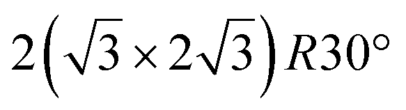 reconstruction, they obtained a nearly complete half-silicane layer (see Fig. 12a).81 Starting from the (4 × 4) reconstruction, they obtained a similar reconstruction where 7 other 18 Si atoms are hydrogenated (see Fig. 12b).66 Remarkably, the hydrogenated silicene sheet can be completely restored to its original state by annealing the sample to a moderate temperature of about 450 K.66,81 Very recently, the hydrogenation of the
  -type II reconstruction has also been reported, with a similar appearance as the one obtained from the
  reconstruction.194 On the contrary, hydrogenation of thick Si films grown on Ag(111) triggers the gradual etching of the surface.195
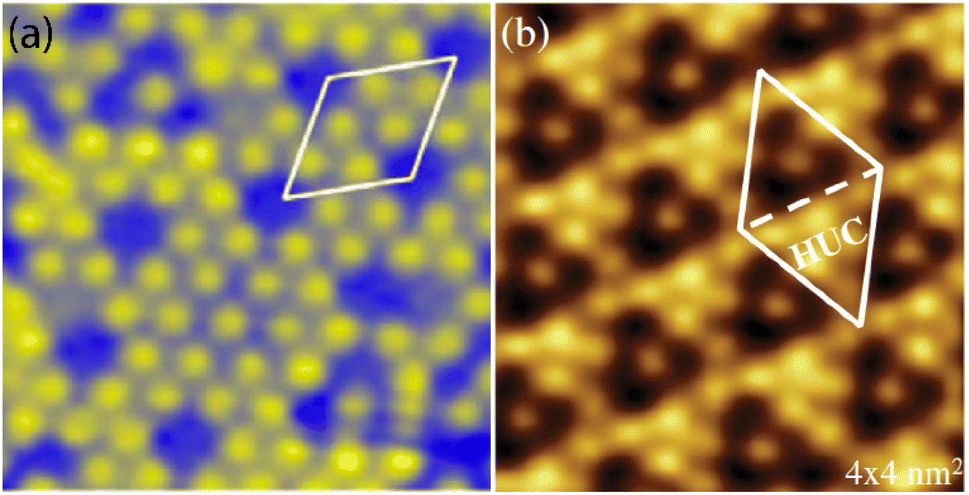 | ||
Fig. 12 STM images of the  (a) and (4 × 4) Si/Ag(111) reconstruction (b) after hydrogen exposure. In (a) the rhombus corresponds to the pristine (a) and (4 × 4) Si/Ag(111) reconstruction (b) after hydrogen exposure. In (a) the rhombus corresponds to the pristine  unit cell, while in (b) it corresponds to a shift of the pristine (4 × 4) unit cell. Adapted with permission from ref. 66, Copyright 2015 by the American Physical Society and with permission from ref. 81, Copyright 2015 American Chemical Society. unit cell, while in (b) it corresponds to a shift of the pristine (4 × 4) unit cell. Adapted with permission from ref. 66, Copyright 2015 by the American Physical Society and with permission from ref. 81, Copyright 2015 American Chemical Society. | ||
Chlorination of silicene layers grown on Ag(111) has been studied by STM.196 Chlorine atoms are found to adsorb on top of the upper buckled Si atoms at low coverage, while, at saturation coverage, the half-chlorinated silicene layer displays a (1 × 1) reconstruction, independently of the initial silicene reconstruction.
Recently, the adsorption at 200 K of potassium atoms has been studied on the silicene (3 × 3)/Ag (4 × 4) reconstruction.197 Whereas K atoms form a dispersed phase at low coverage, they organize into a close-packed layer for a coverage of about 0.17 ML. From STM observations, it was found that the lattice constant of the ordered K layer is the same as the silicene one, while DFT computations indicated that K atoms adsorb on bridge sites, leading to the formation of three different domains equivalent per rotational symmetry (see Fig. 13).
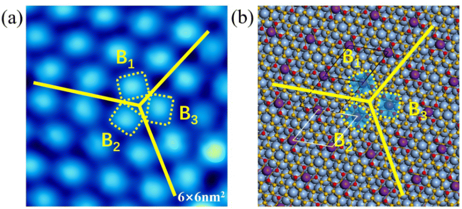 | ||
| Fig. 13 (a) STM image of K atoms adsorbed on silicene/Ag(111) at 200 K. The image shows a boundary between three equivalent domains rotated by ±120°. (b) Structural atomic model proposed. Adapted with permission from ref. 197, Copyright 2022 by the American Physical Society. | ||
The reactivity of epitaxial silicene towards other molecules than dioxygene has been less studied. In 2014, Feng et al. have studied by DFT the adsorption of small molecules on free-standing silicene.198 They have computed adsorption sites, binding energies for CO, NO, NO2, O2, CO2, NH3 and SO2 molecules. Strong adsorption energies were found for NO2, SO2 and O2 molecules, whereas CO was less bound and CO2 only weakly physisorbed. In between, NO and NH3 can be chemically adsorbed on silicene with moderate adsorption energies (1 eV per molecule) making silicene a promising candidate as a sensor for such molecules.198 Following this work, many other studies have been devoted to compute the atomic configurations, adsorption energy and dissociative energy for small molecules on free-standing silicene.199–201 Other theoretical works have been devoted to the functionalization of silicene and hydrogenated-silicene with π chemical functions.202,203 Beside O2 adsorption, there are only few experimental studies of molecular adsorption on silicene. Adsorption and thermal reaction processes of NO with silicene/ZrB2 have been studied by XPS. It has been shown that NO is dissociatively adsorbed at 300 K. Upon NO exposure, the silicene layer is progressively oxidized. After prolonged heating at 1053 K, the silicene layer is reformed but is covered with a BN layer.204 Recently, CoPc adsorption on silicene/Ag(111) has been studied by STM/STS.205
6.3 Dirac fermions in epitaxial silicene
The massless, relativistic behaviour of free-standing silicene's charge carriers – known as Dirac fermions – results from its unique electronic structure, similar to that of graphene, characterized by conical valence and conduction bands that cross at a single point in momentum space, forming the so-called Dirac cones. The observation of such feature, accessible through ARPES measurements, would thus provide evidence that Dirac Fermion character is preserved in epitaxial silicene. Regarding the extensively studied Si/Ag(111) system, linear dispersion around the![[K with combining macron]](https://www.rsc.org/images/entities/char_004b_0304.gif) Si point of the first silicene BZ was firstly reported in 2012 by Vogt et al. using ARPES, associated with the (4 × 4) silicene superstructure.4 This electronic dispersion was attributed to the presence of Dirac fermions in the silicene band, although the Fermi velocity measured, vF = 1.3 × 10⁶ ms−1 was much larger than the one predicted by theory vF = 0.53 × 10⁶ ms−1.28 The authors mentioned that the downshift of the Dirac point by 0.3 eV below the Fermi level could result from an interaction with Ag(111). More precise ARPES measurements have however demonstrated that this linear dispersion corresponds to a surface band originating from the hybridization between Si and Ag orbitals. This surface band shows a steep linear dispersion around the Ag point (see Fig. 14c) and a saddle point at the
Si point of the first silicene BZ was firstly reported in 2012 by Vogt et al. using ARPES, associated with the (4 × 4) silicene superstructure.4 This electronic dispersion was attributed to the presence of Dirac fermions in the silicene band, although the Fermi velocity measured, vF = 1.3 × 10⁶ ms−1 was much larger than the one predicted by theory vF = 0.53 × 10⁶ ms−1.28 The authors mentioned that the downshift of the Dirac point by 0.3 eV below the Fermi level could result from an interaction with Ag(111). More precise ARPES measurements have however demonstrated that this linear dispersion corresponds to a surface band originating from the hybridization between Si and Ag orbitals. This surface band shows a steep linear dispersion around the Ag point (see Fig. 14c) and a saddle point at the ![[M with combining macron]](https://www.rsc.org/images/entities/char_004d_0304.gif) Ag point (see Fig. 14d) of the first Ag(111) BZ.13,14,168 Finally, ARPES measurements on the same system performed by Feng et al. revealed that this surface band forms six pairs of Dirac cones at the edges of the Ag(111) first BZ (see Fig. 14e and f).206,207
Ag point (see Fig. 14d) of the first Ag(111) BZ.13,14,168 Finally, ARPES measurements on the same system performed by Feng et al. revealed that this surface band forms six pairs of Dirac cones at the edges of the Ag(111) first BZ (see Fig. 14e and f).206,207
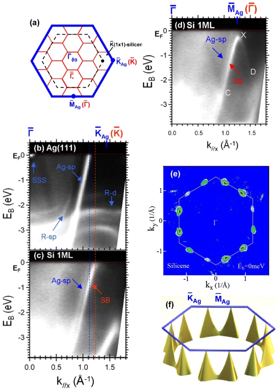 | ||
Fig. 14 (a) BZ scheme of the silicene layer with respect to the Ag(111) surface. (b and c) ARPES intensity maps recorded along the ![[capital Gamma, Greek, macron]](https://www.rsc.org/images/entities/char_e0ba.gif) Ag direction of the Ag(111) BZ for the (b) clean and (c) silicene covered surfaces. Dashed blue and red lines indicate the k//x points at which the bulk Ag sp-band and surface band (SB) cross the Fermi level. (d) ARPES intensity maps recorded along the Ag direction of the Ag(111) BZ for the silicene covered surface. (e) ARPES intensity map at the Fermi level. (f) Schematic 3D diagram showing the 12 Dirac cones in silicene(3 × 3)/Ag(111) forming 6 pairs along the first BZ edges of the Ag(111) surface (thick blue line). Adapted from ref. 14, with permission of AIP Publishing and with permission from ref. 206. Ag direction of the Ag(111) BZ for the (b) clean and (c) silicene covered surfaces. Dashed blue and red lines indicate the k//x points at which the bulk Ag sp-band and surface band (SB) cross the Fermi level. (d) ARPES intensity maps recorded along the Ag direction of the Ag(111) BZ for the silicene covered surface. (e) ARPES intensity map at the Fermi level. (f) Schematic 3D diagram showing the 12 Dirac cones in silicene(3 × 3)/Ag(111) forming 6 pairs along the first BZ edges of the Ag(111) surface (thick blue line). Adapted from ref. 14, with permission of AIP Publishing and with permission from ref. 206. | ||
The theoretical interpretation of ARPES spectra obtained for epitaxial silicene on Ag(111) has received particular interest. Several band structure calculations by means of DFT pointed out that the linear dispersion observed in ARPES spectra at the Si point of the silicene first BZ could not be attributed to the presence of Dirac cones, but was rather due to strong hybridization between silicene and Ag,11 Ag substrate states modified by interactions with the silicene overlayer,12 or Ag-derived bands.208,209 DFT calculations combined with orbital-selective band unfolding techniques also demonstrated the presence of 6 pairs of Dirac cones at the edges of the Ag first BZ, induced by the hybridization between Si pz orbitals and Ag sp bands.210,211
Band structures presenting similar features with the one of graphene were also reported by ARPES for epitaxial silicene on ZrB2(0001) and Au(111).15,133 For silicene on ZrB2(0001), DFT computations showed that all silicene-derived bands are hybridized with Zr d electronic states.148 For silicene on Au(111), the linear dispersion was associated with the (12 × 12) reconstruction observed by LEED.133
A special attention was paid to the electronic structure of Si NRs grown on Ag(110). A linear dispersion close to the Fermi level and near the ![[X with combining macron]](https://www.rsc.org/images/entities/char_0058_0304.gif) point of the Ag surface BZ has been initially reported.99 However, it was later associated with the folding of Ag states due to the surface reconstruction.208 The electronic structure of the Si NRs has been recently revisited following the elucidation of their atomic structure.115,212 The presence of 1D Dirac fermions has been reported, with Dirac cones crossing at 0.8 eV below the Fermi level and a strong Si pz character.212
point of the Ag surface BZ has been initially reported.99 However, it was later associated with the folding of Ag states due to the surface reconstruction.208 The electronic structure of the Si NRs has been recently revisited following the elucidation of their atomic structure.115,212 The presence of 1D Dirac fermions has been reported, with Dirac cones crossing at 0.8 eV below the Fermi level and a strong Si pz character.212
Finally, ARPES spectra exhibiting linearly dispersion bands were also reported by De Padova et al. for claimed epitaxial multilayer silicene grown on Ag(110) and Ag(111).153,156
To conclude, the interpretation of ARPES spectra requires the precise knowledge of the atomic structure of the silicon epitaxial layers. For all systems thoroughly studied, theoretical and experimental investigations pointed out that silicene–substrate interaction cannot be neglected and has to be considered to interpret the band structure measured by ARPES.
6.4 Towards free-standing silicene
Hybridization between silicene and metallic surfaces, which are most commonly used as substrates for silicene synthesis in current experiments, has been reported both theoretically and experimentally, questioning whether silicene maintains its Dirac fermion character, similar to graphene, on a supporting substrate.11,13,14,35,63,71,213 Electronic decoupling from the underlying substrate is thus demanding prior to the incorporation of silicene into devices. Such decoupling can be achieved through the formation of a buffer layer, chemical intercalation leading to possible exfoliation of epitaxial silicene from the underlying substrate or etching of the latter. These processes are quite challenging since the interaction with the underlying substrate tends to stabilize the metastable silicene structure.33,84 Indeed, few experimental works have been reported in the literature.In 2016, Du et al. have proposed to isolate the silicene layer from the Ag(111) substrate through intercalation with oxygen.184 In their experiments, a sample covered with various phases, namely  or (4 × 4) silicene/Ag(111) reconstructions and thick Si films (with
  Si reconstruction) was exposed to O2 at RT, up to 1200 L. STM, XPS and Raman spectroscopy showed that silicene monolayers were fully oxidized, whereas thicker layers (assumed to be silicene bilayers) resisted to oxidation and remained ordered, with a change from a
  reconstruction to a (1 × 1) one, relatively to a silicene plane (see Fig. 15a, b and e (bottom)). These results were interpreted in the framework of the intercalation of oxygen atoms at the interface between the bilayer and the substrate, leading to the oxidation of the interfacial Si layer and the decoupling of the oxide-free silicene layer from the substrate, which was supported by DFT calculations (see Fig. 15c–e (top)). However, it should be noted that the different behavior observed between monolayer and bilayer silicene could also be explained by the Ag termination of the bilayer that would protect the surface against oxidation.
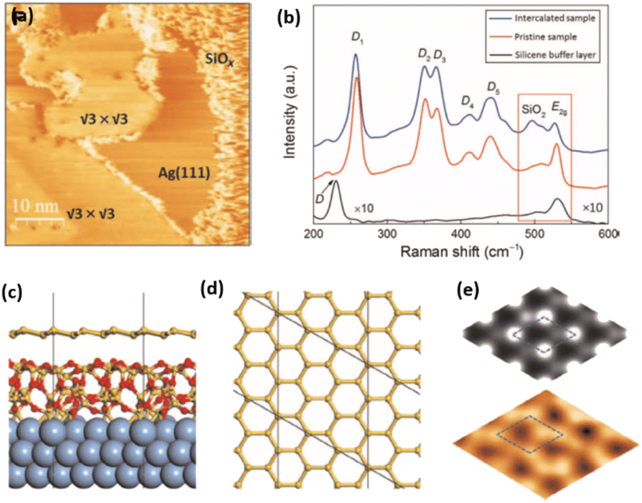 | ||
| Fig. 15 Oxygen-intercalated epitaxial silicene grown on Ag(111). (a) STM image after an oxygen dose of 1200 L: the silicene monolayer is fully oxidized (SiOx) while the top √3 × √3 of bilayer silicene exhibits structural stability. (b) Raman spectra of silicene interfacial (buffer) layer, pristine bilayer silicene and oxygen-intercalated bilayer silicene. The E2g Raman peak is the signature of silicene structures. After oxygen exposure, an additional Raman peak emerges, assigned to the oxidation of the silicene interfacial layer. (c and d) Atomic structure of silicene/SiOx/Ag(111) from AIMD simulation: side view (c) and top view of the top silicene layer (d). Oxygen atoms are drawn in red and Si atoms in yellow-brown. (e) Simulated (top) and experimental (bottom) STM images of silicene/SiOx/Ag(111), showing a (1 × 1) honeycomb lattice assigned to free-standing silicene. Adapted with permission from AAAS, from ref. 184, Copyright The Authors, some rights reserved; exclusive licensee AAAS. Distributed under a CC BY-NC 4.0 license. | ||
It has to be mentioned that reducing the interaction of silicene with the substrate by means of intercalants raises the question of possible exfoliation of the silicene, as put forward by Tsetseris et al. in a theoretical study on Ca intercalation.214 One major concern would be that silicene retains its 2D structure once detached from the underlying substrate.
The next step to implement silicene in an operating device would be its transfer on a target substrate. This task was addressed by Tao, Molle and co-workers in 2015.215 The authors have devised a growth-transfer-fabrication process denoted “silicene encapsulated delamination with native electrodes” (SEDNE) in order to fabricate a field-effect transistor (FET) (see Fig. 16). In this process, the expensive bulk single-crystal Ag was replaced by a thin film of Ag(111) deposited on mica. The epitaxial silicene layer on Ag(111) was thus capped in situ with an alumina film, followed by the ex situ delamination of the silver–silicene–alumina sandwich and the flip transfer onto a device substrate (SiO2/p++ doped Si). It has to be underlined that the silver–silicene–alumina sandwich has allowed the preservation of the silicene layer during the delamination transfer, as shown by Raman spectroscopy. The final step consisted in the patterning of the silicene channel and the source/drain electrodes in the native Ag film using electron beam lithography and a specially devised Ag etchant to prevent rapid degradation/oxidation of the silicene layer. This last process allowed electrical measurements of a Ag-free silicene device before its degradation in ∼2 min in air. This device showed ambipolar Dirac charge transport at RT, similar to graphene FET, but with a low mobility of ∼100 cm2 V−1 s−1, attributed to acoustic phonon-limited transport and grain boundary scattering. Other approaches based on the alumina/silicene/Ag/mica stack for disassembling epitaxial silicene from Ag(111) and transferring onto target substrates have been recently devised by Martella, Molle and co-workers.216
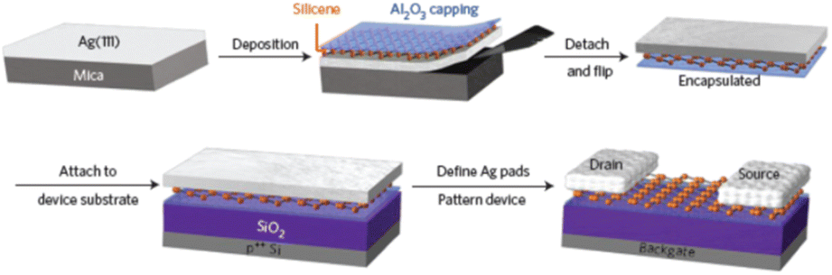 | ||
| Fig. 16 Schematics of growth-transfer-fabrication process denoted “silicene encapsulated delamination with native electrodes” (SEDNE). See text for the description of the different steps. Adapted with permission from ref. 215, Springer Nature. | ||
As a conclusion, the achievement of long-term stable quasi-freestanding silicene is still an on-going challenge. Although decoupling of epitaxial silicene from the underlying substrate has been reported, the integration of silicene in operational devices would require to address several locks related to the structural and chemical stability of silicene layers. Moreover, the growth of large-scale, high-quality and single crystalline silicene sheets also appears as a critical issue.
7. Conclusions
Research into the synthesis of silicene, a 2D layer of Si atoms arranged in a low-buckled honeycomb structure, has attracted a great deal of interest from the scientific community over the last decade, and major advances have been obtained in this direction. The large consensus obtained on the nature of silicene/Ag(111) has been obtained thanks to the combined efforts of many different experimental techniques associated with DFT calculations. In particular the association of real-space imaging techniques such as STM or AFM with diffraction methods such as LEED-I(V) or SXRD and with thermodynamical studies has proven to be efficient for the structural determination. However, for a large fraction of systems, epitaxial growth of silicene has been reported only on the basis of STM analysis. Usually, the model proposed are relaxed by DFT in order to verify its metastability. Comparisons with possible models that could be more stable, in particular for which the silicene lattice constant would be closer to the one of free-standing silicene, are rarely performed. Most surprisingly, straightforward simulations of STM images, in the usual Tersoff–Hamann approximation are not systematically undertaken. Contradictory results reported for some epitaxial systems may arise from such incomplete characterization. It has to be noted that co-existence of several Si reconstructions on a substrate are often reported in the literature. Therefore, a better understanding of silicene growth mechanisms is needed to master the synthesis of large-scale uniform silicene layers with a high degree of structural order at the atomic scale.Despite the reported successes in the epitaxial growth of low-buckled honeycomb Si layers, the synthesis of free-standing silicene remains a major challenge for verification of theoretical predictions. An appropriate substrate allowing the growth of honeycomb structures while preserving the Dirac cone is still demanding. Thus, to date, the question of whether silicene can be considered as the analogue of graphene regarding its electronic properties (Dirac cone, high Fermi velocity and carrier mobility) or as a complementary 2D material remains open.
Abbreviations
| 1D | One-dimensional |
| 2D | Two-dimensional |
| 3D | Three-dimensional |
| AES | Auger electron spectroscopy |
| AFM | Atomic force microscopy |
| AIMD | Ab initio molecular dynamics |
| ALD | Atomic layer deposition |
| ARPES | Angle-resolved photoelectron spectroscopy |
| BLG | Bilayer graphene |
| BZ | Brillouin zone |
| DB | Dumbbell |
| DFT | Density-functional theory |
| DNR | Double nanoribbon |
| EXAFS | Extended X-ray absorption fine structure |
| FET | Field-effect transistor |
| h-BN | Hexagonal boron nitride |
| HCT | Honeycomb-chain triangle |
| HOPG | Highly oriented pyrolytic graphite |
| HREELS | High resolution electron energy loss spectroscopy |
| KMC | Kinetic Monte-Carlo |
| LEED | Low-energy electron diffraction |
| LEEM | Low-energy electron microscopy |
| MD | Molecular dynamics |
| ML | Monolayer |
| MR | Missing-row |
| NR | Nanoribbon |
| PES | Photoelectron spectroscopy |
| RAS | Reflectance anisotropy spectroscopy |
| RHEED | Reflection high-energy electron diffraction |
| RT | Room temperature |
| SDRS | Surface differential reflectance spectroscopy |
| SNR | Single nanoribbon |
| STM | Scanning tunneling microscopy |
| STS | Scanning tunneling spectroscopy |
| SXRD | Surface X-ray diffraction |
| TERS | Tip-enhanced Raman spectroscopy |
| UHV | Ultra-high vacuum |
| XPD | X-ray photoelectron diffraction |
| XPS | X-ray photoelectron spectroscopy |
| XRD | X-ray diffraction |
Conflicts of interest
There are no conflicts to declare.Notes and references
- L. Zhang, T. Gong, Z. Yu, H. Dai, Z. Yang, G. Chen, J. Li, R. Pan, H. Wang, Z. Guo, H. Zhang and X. Fu, Adv. Funct. Mater., 2021, 31, 2005471 CrossRef CAS.
- Z. Ni, Q. Liu, K. Tang, J. Zheng, J. Zhou, R. Qin, Z. Gao, D. Yu and J. Lu, Nano Lett., 2012, 12, 113–118 CrossRef CAS PubMed.
- S. Cahangirov, M. Topsakal, E. Aktürk, H. Şahin and S. Ciraci, Phys. Rev. Lett., 2009, 102, 236804 CrossRef CAS PubMed.
- P. Vogt, P. De Padova, C. Quaresima, J. Avila, E. Frantzeskakis, M. C. Asensio, A. Resta, B. Ealet and G. Le Lay, Phys. Rev. Lett., 2012, 108, 155501 CrossRef PubMed.
- K. Takeda and K. Shiraishi, Phys. Rev. B: Condens. Matter Mater. Phys., 1994, 50, 14916–14922 CrossRef CAS PubMed.
- G. Guzmán-Verri and L. Lew Yan Voon, Phys. Rev. B: Condens. Matter Mater. Phys., 2007, 76, 075131 CrossRef.
- C.-C. Liu, W. Feng and Y. Yao, Phys. Rev. Lett., 2011, 107, 076802 CrossRef PubMed.
- B. Feng, Z. Ding, S. Meng, Y. Yao, X. He, P. Cheng, L. Chen and K. Wu, Nano Lett., 2012, 12, 3507–3511 CrossRef CAS PubMed.
- C.-L. Lin, R. Arafune, K. Kawahara, N. Tsukahara, E. Minamitani, Y. Kim, N. Takagi and M. Kawai, Appl. Phys. Express, 2012, 5, 045802 CrossRef.
- H. Jamgotchian, Y. Colignon, N. Hamzaoui, B. Ealet, J. Y. Hoarau, B. Aufray and J. P. Bibérian, J. Phys.: Condens. Matter, 2012, 24, 172001 CrossRef CAS PubMed.
- S. Cahangirov, M. Audiffred, P. Tang, A. Iacomino, W. Duan, G. Merino and A. Rubio, Phys. Rev. B: Condens. Matter Mater. Phys., 2013, 88, 035432 CrossRef.
- M. X. Chen and M. Weinert, Nano Lett., 2014, 14, 5189–5193 CrossRef CAS PubMed.
- S. K. Mahatha, P. Moras, V. Bellini, P. M. Sheverdyaeva, C. Struzzi, L. Petaccia and C. Carbone, Phys. Rev. B: Condens. Matter Mater. Phys., 2014, 89, 201416(R) CrossRef.
- D. Tsoutsou, E. Xenogiannopoulou, E. Golias, P. Tsipas and A. Dimoulas, Appl. Phys. Lett., 2013, 103, 231604 CrossRef.
- A. Fleurence, R. Friedlein, T. Ozaki, H. Kawai, Y. Wang and Y. Yamada-Takamura, Phys. Rev. Lett., 2012, 108, 245501 CrossRef PubMed.
- L. Meng, Y. Wang, L. Zhang, S. Du, R. Wu, L. Li, Y. Zhang, G. Li, H. Zhou, W. A. Hofer and H.-J. Gao, Nano Lett., 2013, 13, 685–690 CrossRef CAS PubMed.
- T. Aizawa, S. Suehara and S. Otani, J. Phys. Chem. C, 2014, 118, 23049–23057 CrossRef CAS.
- D. Chiappe, E. Scalise, E. Cinquanta, C. Grazianetti, B. van den Broek, M. Fanciulli, M. Houssa and A. Molle, Adv. Mater., 2014, 26, 2096–2101 CrossRef CAS PubMed.
- L. Huang, Y.-F. Zhang, Y.-Y. Zhang, W. Xu, Y. Que, E. Li, J.-B. Pan, Y.-L. Wang, Y. Liu, S.-X. Du, S. T. Pantelides and H.-J. Gao, Nano Lett., 2017, 17, 1161–1166 CrossRef CAS PubMed.
- A. Stępniak-Dybala, P. Dyniec, M. Kopciuszyski, R. Zdyb, M. Jałochowski and M. Krawiec, Adv. Funct. Mater., 2019, 29, 1906053 CrossRef.
- A. Stępniak-Dybala and M. Krawiec, J. Phys. Chem. C, 2019, 123, 17019–17025 CrossRef.
- G. Prévot, C. Hogan, T. Leoni, R. Bernard, E. Moyen and L. Masson, Phys. Rev. Lett., 2016, 117, 276102 CrossRef PubMed.
- T. Leoni, C. Hogan, K. Zhang, M. Daher Mansour, R. Bernard, R. Parret, A. Resta, S. Colonna, Y. Borensztein, F. Ronci, G. Prévot and L. Masson, J. Phys. Chem. C, 2021, 125, 17906–17917 CrossRef CAS.
- Y. Sassa, F. O. L. Johansson, A. Lindblad, M. G. Yazdi, K. Simonov, J. Weissenrieder, M. Muntwiler, F. Iyikanat, H. Sahin, T. Angot, E. Salomon and G. Le Lay, Appl. Surf. Sci., 2020, 530, 147195 CrossRef CAS.
- P. De Padova, P. Vogt, A. Resta, J. Avila, I. Razado-Colambo, C. Quaresima, C. Ottaviani, B. Olivieri, T. Bruhn, T. Hirahara, T. Shirai, S. Hasegawa, M. Carmen Asensio and G. Le Lay, Appl. Phys. Lett., 2013, 102, 163106 CrossRef.
- C. Grazianetti, E. Cinquanta, L. Tao, P. De Padova, C. Quaresima, C. Ottaviani, D. Akinwande and A. Molle, ACS Nano, 2017, 11, 3376–3382 CrossRef CAS PubMed.
- S. Chowdhury and D. Jana, Rep. Prog. Phys., 2016, 79, 126501 CrossRef PubMed.
- F. Bechstedt, P. Gori and O. Pulci, Prog. Surf. Sci., 2021, 96, 100615 CrossRef CAS.
- J. Zhao, H. Liu, Z. Yu, R. Quhe, S. Zhou, Y. Wang, C. C. Liu, H. Zhong, N. Han, J. Lu, Y. Yao and K. Wu, Prog. Mater. Sci., 2016, 83, 24–151 CrossRef CAS.
- A. Molle, C. Grazianetti, L. Tao, D. Taneja, Md. H. Alam and D. Akinwande, Chem. Soc. Rev., 2018, 47, 6370–6387 RSC.
- M. A. Kharadi, G. F. A. Malik, F. A. Khanday, K. A. Shah, S. Mittal and B. K. Kaushik, ECS J. Solid State Sci. Technol., 2020, 9, 115031 CrossRef CAS.
- A. Curcella, R. Bernard, Y. Borensztein, A. Resta, M. Lazzeri and G. Prevot, Phys. Rev. B: Condens. Matter Mater. Phys., 2016, 94, 165438 CrossRef.
- A. Curcella, R. Bernard, Y. Borensztein, A. Resta, M. Lazzeri and G. Prévot, Phys. Rev. B: Condens. Matter Mater. Phys., 2019, 99, 205411 CrossRef CAS.
- C. Léandri, H. Oughaddou, B. Aufray, J. M. Gay, G. Le Lay, A. Ranguis and Y. Garreau, Surf. Sci., 2007, 601, 262–267 CrossRef.
- Y. Sato, Y. Fukaya, M. Cameau, A. K. Kundu, D. Shiga, R. Yukawa, K. Horiba, C.-H. Chen, A. Huang, H.-T. Jeng, T. Ozaki, H. Kumigashira, M. Niibe and I. Matsuda, Phys. Rev. Mater., 2020, 4, 064005 CrossRef CAS.
- T. Jaroch, M. Krawiec and R. Zdyb, 2D Mater., 2021, 8, 035038 CrossRef CAS.
- D. Nazzari, J. Genser, V. Ritter, O. Bethge, E. Bertagnolli, G. Ramer, B. Lendl, K. Watanabe, T. Taniguchi, R. Rurali, M. Kolíbal and A. Lugstein, J. Phys. Chem. C, 2021, 125, 9973–9980 CrossRef CAS PubMed.
- M. Rachid Tchalala, H. Enriquez, A. J. Mayne, A. Kara, S. Roth, M. G. Silly, A. Bendounan, F. Sirotti, T. Greber, B. Aufray, G. Dujardin, M. Ait Ali and H. Oughaddou, Appl. Phys. Lett., 2013, 102, 083107 CrossRef.
- M. De Crescenzi, I. Berbezier, M. Scarselli, P. Castrucci, M. Abbarchi, A. Ronda, F. Jardali, J. Park and H. Vach, ACS Nano, 2016, 10, 11163 CrossRef CAS PubMed.
- N. Yue, J. Myers, L. Su, W. Wang, F. Liu, R. Tsu, Y. Zhuang and Y. Zhang, J. Semicond., 2019, 40, 062001 CrossRef CAS.
- D. Nicholls, Fatima, D. Çakır and N. Oncel, J. Phys. Chem. C, 2019, 123, 7225–7229 CrossRef CAS.
- K. Quertite, H. Enriquez, N. Trcera, Y. Tong, A. Bendounan, A. J. Mayne, G. Dujardin, P. Lagarde, A. El kenz, A. Benyoussef, Y. J. Dappe, A. Kara and H. Oughaddou, Adv. Funct. Mater., 2021, 2007013 CrossRef CAS.
- G. Li, L. Zhang, W. Xu, J. Pan, S. Song, Y. Zhang, H. Zhou, Y. Wang, L. Bao, Y.-Y. Zhang, S. Du, M. Ouyang, S. T. Pantelides and H.-J. Gao, Adv. Mater., 2018, 30, 1804650 CrossRef PubMed.
- C.-C. Lee, A. Fleurence, R. Friedlein, Y. Yamada-Takamura and T. Ozaki, Phys. Rev. B: Condens. Matter Mater. Phys., 2014, 90, 241402(R) CrossRef.
- F. B. Wiggers, A. Fleurence, K. Aoyagi, T. Yonezawa, Y. Yamada-Takamura, H. Feng, J. Zhuang, Y. Du, A. Y. Kovalgin and M. P. de Jong, 2D Mater., 2019, 6, 035001 CrossRef CAS.
- Z. Li, H. Feng, J. Zhuang, N. Pu, L. Wang, X. Xu, W. Hao and Y. Du, J. Phys.: Condens. Matter, 2016, 28, 034002 CrossRef PubMed.
- Z.-L. Liu, M.-X. Wang, J.-P. Xu, J.-F. Ge, G. L. Lay, P. Vogt, D. Qian, C.-L. Gao, C. Liu and J.-F. Jia, New J. Phys., 2014, 16, 075006 CrossRef CAS.
- M. R. Tchalala, H. Enriquez, H. Yildirim, A. Kara, A. J. Mayne, G. Dujardin, M. A. Ali and H. Oughaddou, Appl. Surf. Sci., 2014, 303, 61–66 CrossRef CAS.
- H. Jamgotchian, B. Ealet, Y. Colignon, H. Maradj, J.-Y. Hoarau, J.-P. Biberian and B. Aufray, J. Phys.: Condens. Matter, 2015, 27, 395002 CrossRef CAS PubMed.
- J. Onoda, K. Yabuoshi, H. Miyazaki and Y. Sugimoto, Phys. Rev. B: Condens. Matter Mater. Phys., 2017, 96, 241302(R) CrossRef.
- R. Pawlak, C. Drechsel, P. D'Astolfo, M. Kisiel, E. Meyer and J. I. Cerda, Proc. Natl. Acad. Sci., 2020, 117, 228–237 CrossRef CAS PubMed.
- J. Onoda, L. Feng, K. Yabuoshi and Y. Sugimoto, Phys. Rev. Mater., 2019, 3, 104002 CrossRef CAS.
- P. Moras, T. O. Mentes, P. M. Sheverdyaeva, A. Locatelli and C. Carbone, J. Phys.: Condens. Matter, 2014, 26, 185001 CrossRef CAS PubMed.
- D. Chiappe, C. Grazianetti, G. Tallarida, M. Fanciulli and A. Molle, Adv. Mater., 2012, 24, 5088–5093 CrossRef CAS PubMed.
- R. Arafune, C.-L. Lin, K. Kawahara, N. Tsukahara, E. Minamitani, Y. Kim, N. Takagi and M. Kawai, Surf. Sci., 2013, 608, 297–300 CrossRef CAS.
- G.-W. Lee, H.-D. Chen and D.-S. Lin, Appl. Surf. Sci., 2015, 354, 187–195 CrossRef CAS.
- Y. Fukaya, I. Mochizuki, M. Maekawa, K. Wada, T. Hyodo, I. Matsuda and A. Kawasuso, Phys. Rev. B: Condens. Matter Mater. Phys., 2013, 88, 205413 CrossRef.
- K. Kawahara, T. Shirasawa, R. Arafune, C.-L. Lin, T. Takahashi, M. Kawai and N. Takagi, Surf. Sci., 2014, 623, 25–28 CrossRef CAS.
- Z. Majzik, M. Rachid Tchalala, M. Švec, P. Hapala, H. Enriquez, A. Kara, A. J. Mayne, G. Dujardin, P. Jelínek and H. Oughaddou, J. Phys.: Condens. Matter, 2013, 25, 225301 CrossRef CAS PubMed.
- H. Enriquez, S. Vizzini, A. Kara, B. Lalmi and H. Oughaddou, J. Phys.: Condens. Matter, 2012, 24, 314211 CrossRef PubMed.
- P. Pflugradt, L. Matthes and F. Bechstedt, Phys. Rev. B: Condens. Matter Mater. Phys., 2014, 89, 035403 CrossRef.
- S. Cahangirov, V. O. Özçelik, L. Xian, J. Avila, S. Cho, M. C. Asensio, S. Ciraci and A. Rubio, Phys. Rev. B: Condens. Matter Mater. Phys., 2014, 90, 035448 CrossRef CAS.
- Z.-X. Guo, S. Furuya, J. Iwata and A. Oshiyama, Phys. Rev. B: Condens. Matter Mater. Phys., 2013, 87, 235435 CrossRef.
- L. Chun-Liang, A. Ryuichi, K. Maki and T. Noriaki, Chin. Phys. B, 2015, 24, 087307 CrossRef.
- C.-L. Lin, R. Arafune, M. Kawai and N. Takagi, Chin. Phys. B, 2015, 24, 087307 CrossRef.
- J. Qiu, H. Fu, Y. Xu, A. I. Oreshkin, T. Shao, H. Li, S. Meng, L. Chen and K. Wu, Phys. Rev. Lett., 2015, 114, 126101 CrossRef PubMed.
- R. Stephan, M.-C. Hanf and P. Sonnet, J. Phys.: Condens. Matter, 2015, 27, 015002 CrossRef CAS PubMed.
- H. Liu, N. Han and J. Zhao, Appl. Surf. Sci., 2017, 409, 97–101 CrossRef CAS.
- P. M. Sheverdyaeva, S. Kr. Mahatha, P. Moras, L. Petaccia, G. Fratesi, G. Onida and C. Carbone, ACS Nano, 2017, 11, 975–982 CrossRef CAS PubMed.
- Y. Oh, Y. Cho, H. Kwon, J. Lee, I. Jeon, W. Ko, H. W. Kim, J. Ku, G. Kim, H. Suh and S. W. Hwang, Appl. Phys. Lett., 2017, 110, 263112 CrossRef.
- N. W. Johnson, P. Vogt, A. Resta, P. De Padova, I. Perez, D. Muir, E. Z. Kurmaev, G. Le Lay and A. Moewes, Adv. Funct. Mater., 2014, 24, 5253–5259 CrossRef CAS.
- D. Kaltsas, L. Tsetseris and A. Dimoulas, Appl. Surf. Sci., 2014, 291, 93–97 CrossRef CAS.
- Y. Yuan, R. Quhe, J. Zheng, Y. Wang, Z. Ni, J. Shi and J. Lu, Phys. E, 2014, 58, 38–42 CrossRef CAS.
- H. Jamgotchian, B. Ealet, H. Maradj, J.-Y. Hoarau, J.-P. Bibérian and B. Aufray, J. Phys.: Condens. Matter, 2016, 28, 195002 CrossRef CAS PubMed.
- L. Feng, K. Yabuoshi, Y. Sugimoto, J. Onoda, M. Fukuda and T. Ozaki, Phys. Rev. B: Condens. Matter Mater. Phys., 2018, 98, 195311 CrossRef CAS.
- A. Resta, T. Leoni, C. Barth, A. Ranguis, C. Becker, T. Bruhn, P. Vogt and G. Le Lay, Sci. Rep., 2013, 3, 2399 CrossRef PubMed.
- B. Lalmi, H. Oughaddou, H. Enriquez, A. Kara, S. Vizzini, B. Ealet and B. Aufray, Appl. Phys. Lett., 2010, 97, 223109 CrossRef.
- G. Le Lay, P. De Padova, A. Resta, T. Bruhn and P. Vogt, J. Phys. D: Appl. Phys., 2012, 45, 392001 CrossRef.
- H. Jamgotchian, Y. Colignon, B. Ealet, B. Parditka, J.-Y. Hoarau, C. Girardeaux, B. Aufray and J.-P. Bibérian, J. Phys. Conf. Ser., 2014, 491, 012001 CrossRef CAS.
- Z.-L. Liu, M.-X. Wang, C. Liu, J.-F. Jia, P. Vogt, C. Quaresima, C. Ottaviani, B. Olivieri, P. De Padova and G. L. Lay, APL Mater., 2014, 2, 092513 CrossRef.
- J. Qiu, H. Fu, Y. Xu, Q. Zhou, S. Meng, H. Li, L. Chen and K. Wu, ACS Nano, 2015, 9, 11192–11199 CrossRef CAS PubMed.
- R. Bernard, Y. Borensztein, H. Cruguel, M. Lazzeri and G. Prevot, Phys. Rev. B: Condens. Matter Mater. Phys., 2015, 92, 045415 CrossRef.
- C. Grazianetti, D. Chiappe, E. Cinquanta, G. Tallarida, M. Fanciulli and A. Molle, Appl. Surf. Sci., 2014, 291, 109–112 CrossRef CAS.
- J. Gao and J. Zhao, Sci. Rep., 2012, 2, 861 CrossRef PubMed.
- S. Sheng, J. Wu, X. Cong, W. Li, J. Gou, Q. Zhong, P. Cheng, P. Tan, L. Chen and K. Wu, Phys. Rev. Lett., 2017, 119, 196803 CrossRef PubMed.
- G. Prévot, R. Bernard, H. Cruguel and Y. Borensztein, Appl. Phys. Lett., 2014, 105, 213106 CrossRef.
- M. Satta, S. Colonna, R. Flammini, A. Cricenti and F. Ronci, Phys. Rev. Lett., 2015, 115, 026102 CrossRef PubMed.
- P. Lagarde, M. Chorro, D. Roy and N. Trcera, J. Phys.: Condens. Matter, 2016, 28, 075002 CrossRef CAS PubMed.
- Md. S. Rahman, T. Nakagawa and S. Mizuno, Jpn. J. Appl. Phys., 2015, 54, 015502 CrossRef.
- J. T. Küchle, A. Baklanov, A. P. Seitsonen, P. T. P. Ryan, P. Feulner, P. Pendem, T.-L. Lee, M. Muntwiler, M. Schwarz, F. Haag, J. V. Barth, W. Auwärter, D. A. Duncan and F. Allegretti, 2D Mater., 2022, 9, 045021 CrossRef.
- D. Kaltsas, L. Tsetseris and A. Dimoulas, J. Phys.: Condens. Matter, 2012, 24, 442001 CrossRef CAS PubMed.
- J. Sone, T. Yamagami, Y. Aoki, K. Nakatsuji and H. Hirayama, New J. Phys., 2014, 16, 095004 CrossRef CAS.
- H. Shu, D. Cao, P. Liang, X. Wang, X. Chen and W. Lu, Phys. Chem. Chem. Phys., 2014, 16, 304–310 RSC.
- X. Xu, J. Zhuang, Y. Du, S. Eilers, G. Peleckis, W. Yeoh, X. Wang, S. X. Dou and K. Wu, in 2014 International Conference on Nanoscience and Nanotechnology, IEEE, Adelaide, SA, 2014, pp. 28–30 Search PubMed.
- H. Liu, H. Feng, Y. Du, J. Chen, K. Wu and J. Zhao, 2D Mater., 2016, 3, 025034 CrossRef.
- C. Grazianetti, D. Chiappe, E. Cinquanta, M. Fanciulli and A. Molle, J. Phys.: Condens. Matter, 2015, 27, 255005 CrossRef CAS PubMed.
- A. Acun, B. Poelsema, H. J. W. Zandvliet and R. van Gastel, Appl. Phys. Lett., 2013, 103, 263119 CrossRef.
- N. Kawakami, R. Arafune, E. Minamitani, K. Kawahara, N. Takagi and C.-L. Lin, Nanoscale, 2022, 14, 14623–14629 RSC.
- P. De Padova, C. Quaresima, C. Ottaviani, P. M. Sheverdyaeva, P. Moras, C. Carbone, D. Topwal, B. Olivieri, A. Kara, H. Oughaddou, B. Aufray and G. Le Lay, Appl. Phys. Lett., 2010, 96, 261905 CrossRef.
- C. Leandri, G. L. Lay, B. Aufray, C. Girardeaux, J. Avila, M. E. Dávila, M. C. Asensio, C. Ottaviani and A. Cricenti, Surf. Sci., 2005, 574, L9–L15 CrossRef CAS.
- H. Sahaf, L. Masson, C. Léandri, B. Aufray, G. Le Lay and F. Ronci, Appl. Phys. Lett., 2007, 90, 263110 CrossRef.
- G. Le Lay, B. Aufray, C. Léandri, H. Oughaddou, J.-P. Biberian, P. De Padova, M. E. Dávila, B. Ealet and A. Kara, Appl. Surf. Sci., 2009, 256, 524–529 CrossRef CAS.
- F. Ronci, S. Colonna, A. Cricenti, P. De Padova, C. Ottaviani, C. Quaresima, B. Aufray and G. Le Lay, Phys. Status Solidi C, 2010, 7, 2716–2719 CrossRef CAS.
- S. Colonna, G. Serrano, P. Gori, A. Cricenti and F. Ronci, J. Phys.: Condens. Matter, 2013, 25, 315301 CrossRef CAS PubMed.
- R. Bernard, T. Leoni, A. Wilson, T. Lelaidier, H. Sahaf, E. Moyen, L. Assaud, L. Santinacci, F. Leroy, F. Cheynis, A. Ranguis, H. Jamgotchian, C. Becker, Y. Borensztein, M. Hanbücken, G. Prévot and L. Masson, Phys. Rev. B: Condens. Matter Mater. Phys., 2013, 88, 121411 CrossRef.
- M. Daher Mansour, R. Parret and L. Masson, J. Vac. Sci. Technol., A, 2018, 36, 061402 CrossRef.
- F. Ronci, G. Serrano, P. Gori, A. Cricenti and S. Colonna, Phys. Rev. B: Condens. Matter Mater. Phys., 2014, 89, 115437 CrossRef.
- G. He, Phys. Rev. B: Condens. Matter Mater. Phys., 2006, 73, 035311 CrossRef.
- B. Aufray, A. Kara, S. Vizzini, H. Oughaddou, C. Léandri, B. Ealet and G. Le Lay, Appl. Phys. Lett., 2010, 96, 183102 CrossRef.
- A. Kara, S. Vizzini, C. Leandri, B. Ealet, H. Oughaddou, B. Aufray and G. LeLay, J. Phys.: Condens. Matter, 2010, 22, 045004 CrossRef PubMed.
- C. Lian and J. Ni, Phys. B, 2012, 407, 4695–4699 CrossRef CAS.
- M. R. Tchalala, H. Enriquez, A. J. Mayne, A. Kara, G. Dujardin, M. A. Ali and H. Oughaddou, J. Phys.: Conf. Ser., 2014, 491, 012002 CrossRef CAS.
- B. Feng, H. Li, S. Meng, L. Chen and K. Wu, Surf. Sci., 2016, 645, 74–79 CrossRef CAS.
- B. Aufray, B. Ealet, H. Jamgotchian, H. Maradj, J.-Y. Hoarau and J.-P. Biberian, in Silicene, ed., M. J. S. Spencer and T. Morishita, Springer International Publishing, Cham, 2016, vol. 235, pp. 183–202 Search PubMed.
- J. I. Cerdá, J. Sławińska, G. Le Lay, A. C. Marele, J. M. Gómez-Rodríguez and M. E. Dávila, Nat. Commun., 2016, 7, 13076 CrossRef PubMed.
- S. Sheng, R. Ma, J. Wu, W. Li, L. Kong, X. Cong, D. Cao, W. Hu, J. Gou, J.-W. Luo, P. Cheng, P.-H. Tan, Y. Jiang, L. Chen and K. Wu, Nano Lett., 2018, 18, 2937–2942 CrossRef CAS PubMed.
- C. Hogan, S. Colonna, R. Flammini, A. Cricenti and F. Ronci, Phys. Rev. B: Condens. Matter Mater. Phys., 2015, 92, 115439 CrossRef.
- E. Speiser, B. Buick, N. Esser, W. Richter, S. Colonna, A. Cricenti and F. Ronci, Appl. Phys. Lett., 2014, 104, 161612 CrossRef.
- Y. Borensztein, G. Prevot and L. Masson, Phys. Rev. B: Condens. Matter Mater. Phys., 2014, 89, 245410 CrossRef.
- P. Espeter, C. Keutner, P. Roese, K. Shamout, U. Berges, G. Wenzel, L. Bignardi, N. F. Kleimeier, H. Zacharias and C. Westphal, Nanotechnology, 2017, 28, 455701 CrossRef PubMed.
- C. Hogan, O. Pulci, P. Gori, F. Bechstedt, D. S. Martin, E. E. Barritt, A. Curcella, G. Prevot and Y. Borensztein, Phys. Rev. B, 2018, 97, 195407 CrossRef CAS.
- V. O. Özçelik and S. Ciraci, J. Phys. Chem. C, 2013, 117, 26305–26315 CrossRef.
- P. Borlido, C. Rödl, M. A. L. Marques and S. Botti, 2D Mater., 2018, 5, 035010 CrossRef.
- C. Léandri, H. Saifi, O. Guillermet and B. Aufray, Appl. Surf. Sci., 2001, 177, 303–306 CrossRef.
- G. He, Surf. Sci., 2009, 603, 2021–2029 CrossRef CAS.
- D. Geng, H. Zhou, S. Yue, Z. Sun, P. Cheng, L. Chen, S. Meng, K. Wu and B. Feng, Nat. Commun., 2022, 13, 7000 CrossRef CAS PubMed.
- K. Zhang, R. Bernard, Y. Borensztein, H. Cruguel and G. Prévot, Phys. Rev. B: Condens. Matter Mater. Phys., 2020, 102, 125418 CrossRef CAS.
- J. Han, D. Jeon and Y. Kuk, Surf. Sci., 1997, 376, 237–244 CrossRef CAS.
- L. Tang, F. Li and Q. Guo, Appl. Surf. Sci., 2011, 258, 1109–1114 CrossRef CAS.
- H. Enriquez, A. Mayne, A. Kara, S. Vizzini, S. Roth, B. Lalmi, A. P. Seitsonen, B. Aufray, T. Greber, R. Belkhou, G. Dujardin and H. Oughaddou, Appl. Phys. Lett., 2012, 101, 021605 CrossRef.
- M. Schmitz, L. Kesper, M. G. H. Schulte, P. Roese, U. Berges and C. Westphal, J. Phys.: Condens. Matter, 2021, 33, 275001 CrossRef CAS PubMed.
- P. Roese, K. Shamout, P. Espeter, R. Hönig, U. Berges and C. Westphal, Appl. Surf. Sci., 2019, 467–468, 580–587 CrossRef CAS.
- S. Sadeddine, H. Enriquez, A. Bendounan, P. Kumar Das, I. Vobornik, A. Kara, A. J. Mayne, F. Sirotti, G. Dujardin and H. Oughaddou, Sci. Rep., 2017, 7, 44400 CrossRef PubMed.
- O. G. Shpyrko, R. Streitel, V. S. K. Balagurusamy, A. Y. Grigoriev, M. Deutsch, B. M. Ocko, M. Meron, B. Lin and P. S. Pershan, Science, 2006, 313, 77–80 CrossRef CAS PubMed.
- O. G. Shpyrko, R. Streitel, V. S. K. Balagurusamy, A. Yu. Grigoriev, M. Deutsch, B. M. Ocko, M. Meron, B. Lin and P. S. Pershan, Phys. Rev. B: Condens. Matter Mater. Phys., 2007, 76, 245436 CrossRef.
- T. Jaroch and R. Zdyb, Materials, 2022, 15, 1610 CrossRef CAS PubMed.
- M. J. Cherukara, B. Narayanan, H. Chan and S. K. R. S. Sankaranarayanan, Nanoscale, 2017, 9, 10186–10192 RSC.
- M. Satta, P. Lacovig, N. Apostol, M. Dalmiglio, F. Orlando, L. Bignardi, H. Bana, E. Travaglia, A. Baraldi, S. Lizzit and R. Larciprete, Nanoscale, 2018, 10, 7085–7094 RSC.
- A. Stępniak-Dybala, M. Jałochowski and M. Krawiec, Condens. Matter, 2016, 1, 8 CrossRef.
- H. Guo, R. Zhang, H. Li, X. Wang, H. Lu, K. Qian, G. Li, L. Huang, X. Lin, Y.-Y. Zhang, H. Ding, S. Du, S. T. Pantelides and H.-J. Gao, Nano Lett., 2020, 20, 2674–2680 CrossRef CAS PubMed.
- R. van Bremen, Q. Yao, S. Banerjee, D. Cakir, N. Oncel and H. J. W. Zandvliet, Beilstein J. Nanotechnol., 2017, 8, 1952–1960 CrossRef CAS PubMed.
- P. Castrucci, F. Fabbri, T. Delise, M. Scarselli, M. Salvato, S. Pascale, R. Francini, I. Berbezier, C. Lechner, F. Jardali, H. Vach and M. De Crescenzi, Nano Res., 2018, 11, 5879–5889 CrossRef CAS.
- Y. Cai, C.-P. Chuu, C. M. Wei and M. Y. Chou, Phys. Rev. B: Condens. Matter Mater. Phys., 2013, 88, 245408 CrossRef.
- F. Jardali, C. Lechner, M. De Crescenzi, M. Scarselli, I. Berbezier, P. Castrucci and H. Vach, Nano Res., 2020, 13, 2378–2383 CrossRef CAS.
- W. Peng, T. Xu, P. Diener, L. Biadala, M. Berthe, X. Pi, Y. Borensztein, A. Curcella, R. Bernard, G. Prévot and B. Grandidier, ACS Nano, 2018, 12, 4754–4760 CrossRef CAS PubMed.
- I. Kupchak, F. Fabbri, M. De Crescenzi, M. Scarselli, M. Salvato, T. Delise, I. Berbezier, O. Pulci and P. Castrucci, Nanoscale, 2019, 11, 6145–6152 RSC.
- C.-C. Lee, A. Fleurence, R. Friedlein, Y. Yamada-Takamura and T. Ozaki, Phys. Rev. B: Condens. Matter Mater. Phys., 2013, 88, 165404 CrossRef.
- C.-C. Lee, A. Fleurence, Y. Yamada-Takamura, T. Ozaki and R. Friedlein, Phys. Rev. B: Condens. Matter Mater. Phys., 2014, 90, 075422 CrossRef CAS.
- T. Aizawa, S. Suehara and S. Otani, J. Phys.: Condens. Matter, 2015, 27, 305002 CrossRef CAS PubMed.
- C.-C. Lee, J. Yoshinobu, K. Mukai, S. Yoshimoto, H. Ueda, R. Friedlein, A. Fleurence, Y. Yamada-Takamura and T. Ozaki, Phys. Rev. B: Condens. Matter Mater. Phys., 2017, 95, 115437 CrossRef.
- A. Fleurence, T. G. Gill, R. Friedlein, J. T. Sadowski, K. Aoyagi, M. Copel, R. M. Tromp, C. F. Hirjibehedin and Y. Yamada-Takamura, Appl. Phys. Lett., 2016, 108, 151902 CrossRef.
- A. Fleurence and Y. Yamada-Takamura, 2D Mater., 2021, 8, 045011 CrossRef CAS.
- P. De Padova, O. Kubo, B. Olivieri, C. Quaresima, T. Nakayama, M. Aono and G. Le Lay, Nano Lett., 2012, 12, 5500–5503 CrossRef CAS PubMed.
- L. Chen, C.-C. Liu, B. Feng, X. He, P. Cheng, Z. Ding, S. Meng, Y. Yao and K. Wu, Phys. Rev. Lett., 2012, 109, 056804 CrossRef PubMed.
- L. Chen, H. Li, B. Feng, Z. Ding, J. Qiu, P. Cheng, K. Wu and S. Meng, Phys. Rev. Lett., 2013, 110, 085504 CrossRef PubMed.
- P. De Padova, J. Avila, A. Resta, I. Razado-Colambo, C. Quaresima, C. Ottaviani, B. Olivieri, T. Bruhn, P. Vogt, M. C. Asensio and G. Le Lay, J. Phys.: Condens. Matter, 2013, 25, 382202 CrossRef PubMed.
- P. Vogt, P. Capiod, M. Berthe, A. Resta, P. De Padova, T. Bruhn, G. Le Lay and B. Grandidier, Appl. Phys. Lett., 2014, 104, 021602 CrossRef.
- P. De Padova, C. Ottaviani, C. Quaresima, B. Olivieri, P. Imperatori, E. Salomon, T. Angot, L. Quagliano, C. Romano, A. Vona, M. Muniz-Miranda, A. Generosi, B. Paci and G. Le Lay, 2D Mater., 2014, 1, 021003 CrossRef CAS.
- P. De Padova, A. Generosi, B. Paci, C. Ottaviani, C. Quaresima, B. Olivieri, E. Salomon, T. Angot and G. Le Lay, 2D Mater., 2016, 3, 031011 CrossRef.
- J. Chen, Y. Du, Z. Li, W. Li, B. Feng, J. Qiu, P. Cheng, S. Xue Dou, L. Chen and K. Wu, Sci. Rep., 2015, 5, 13590 CrossRef CAS PubMed.
- Z.-X. Guo and A. Oshiyama, New J. Phys., 2015, 17, 045028 CrossRef.
- A. J. Mannix, B. Kiraly, B. L. Fisher, M. C. Hersam and N. P. Guisinger, ACS Nano, 2014, 8, 7538–7547 CrossRef CAS PubMed.
- T. Shirai, T. Shirasawa, T. Hirahara, N. Fukui, T. Takahashi and S. Hasegawa, Phys. Rev. B: Condens. Matter Mater. Phys., 2014, 89, 241403 CrossRef.
- K. Kawahara, T. Shirasawa, C.-L. Lin, R. Nagao, N. Tsukahara, T. Takahashi, R. Arafune, M. Kawai and N. Takagi, Surf. Sci., 2016, 651, 70–75 CrossRef CAS.
- A. Curcella, R. Bernard, Y. Borensztein, M. Lazzeri, A. Resta, Y. Garreau and G. Prévot, 2D Mater., 2017, 4, 025067 CrossRef.
- Y. Borensztein, A. Curcella, S. Royer and G. Prévot, Phys. Rev. B: Condens. Matter Mater. Phys., 2015, 92, 155407 CrossRef.
- S. K. Mahatha, P. Moras, P. M. Sheverdyaeva, R. Flammini, K. Horn and C. Carbone, Phys. Rev. B: Condens. Matter Mater. Phys., 2015, 92, 245127 CrossRef.
- S. K. Mahatha, P. Moras, P. M. Sheverdyaeva, V. Bellini, T. O. Menteş, A. Locatelli, R. Flammini, K. Horn and C. Carbone, J. Electron Spectrosc. Relat. Phenom., 2017, 219, 2–8 CrossRef CAS.
- C.-L. Lin, T. Hagino, Y. Ito, K. Kawahara, R. Nagao, M. Aoki, S. Masuda, R. Arafune, M. Kawai and N. Takagi, J. Phys. Chem. C, 2016, 120, 6689–6693 CrossRef CAS.
- K. Yabuoshi and Y. Sugimoto, Jpn. J. Appl. Phys., 2019, 58, 020903 CrossRef CAS.
- H.-D. Chen, K.-H. Chien, C.-Y. Lin, T.-C. Chiang and D.-S. Lin, J. Phys. Chem. C, 2016, 120, 2698–2702 CrossRef CAS.
- A. Curcella, R. Bernard, Y. Borensztein, M. Lazzeri and G. Prévot, Nanoscale, 2018, 10, 2291–2300 RSC.
- A. Curcella, R. Bernard, Y. Borensztein, S. Pandolfi and G. Prévot, Beilstein J. Nanotechnol., 2018, 9, 48–56 CrossRef CAS PubMed.
- P. De Padova, H. Feng, J. Zhuang, Z. Li, A. Generosi, B. Paci, C. Ottaviani, C. Quaresima, B. Olivieri, M. Krawiec and Y. Du, J. Phys. Chem. C, 2017, 121, 27182–27190 CrossRef CAS.
- P. De Padova, A. Generosi, B. Paci, C. Ottaviani, C. Quaresima, B. Olivieri, M. Kopciuszyński, L. Żurawek, R. Zdyb and M. Krawiec, Materials, 2019, 12, 2258 CrossRef CAS PubMed.
- D. Garagnani, P. De Padova, C. Ottaviani, C. Quaresima, A. Generosi, B. Paci, B. Olivieri, M. Jałochowski and M. Krawiec, Materials, 2022, 15, 1730 CrossRef CAS PubMed.
- T. G. Gill, A. Fleurence, B. Warner, H. Prüser, R. Friedlein, J. T. Sadowski, C. F. Hirjibehedin and Y. Yamada-Takamura, 2D Materials, 2017, 4, 021015 CrossRef.
- P. De Padova, C. Quaresima, B. Olivieri, P. Perfetti and G. Le Lay, J. Phys. D: Appl. Phys., 2011, 44, 312001 CrossRef.
- M. R. Tchalala, H. Enriquez, A. Bendounan, A. J. Mayne, G. Dujardin, A. Kara, M. A. Ali and H. Oughaddou, Nanoscale Adv., 2020, 2, 2309–2314 RSC.
- A. Molle, C. Grazianetti, D. Chiappe, E. Cinquanta, E. Cianci, G. Tallarida and M. Fanciulli, Adv. Funct. Mater., 2013, 23, 4340–4344 CrossRef CAS.
- Y. Du, J. Zhuang, H. Liu, X. Xu, S. Eilers, K. Wu, P. Cheng, J. Zhao, X. Pi, K. W. See, G. Peleckis, X. Wang and S. X. Dou, ACS Nano, 2014, 8, 10019–10025 CrossRef CAS PubMed.
- X. Xu, J. Zhuang, Y. Du, H. Feng, N. Zhang, C. Liu, T. Lei, J. Wang, M. Spencer, T. Morishita, X. Wang and S. X. Dou, Sci. Rep., 2014, 4, 7543 CrossRef PubMed.
- T. Morishita and M. J. S. Spencer, Sci. Rep., 2015, 5, 17570 CrossRef CAS PubMed.
- Y. Du, J. Zhuang, J. Wang, Z. Li, H. Liu, J. Zhao, X. Xu, H. Feng, L. Chen, K. Wu, X. Wang and S. X. Dou, Sci. Adv., 2016, 2, e1600067 CrossRef PubMed.
- A. Kandemir, F. Iyikanat, C. Bacaksiz and H. Sahin, Beilstein J. Nanotechnol., 2017, 8, 1808–1814 CrossRef CAS PubMed.
- D. Solonenko, O. Selyshchev, D. R. T. Zahn and P. Vogt, Phys. Status Solidi B, 2019, 256, 1800432 CrossRef.
- A. Molle, G. Faraone, A. Lamperti, D. Chiappe, E. Cinquanta, C. Martella, E. Bonera, E. Scalise and C. Grazianetti, Faraday Discuss., 2021, 227, 171–183 RSC.
- H. Van Bui, F. B. Wiggers, R. Friedlein, Y. Yamada-Takamura, A. Y. Kovalgin and M. P. de Jong, J. Chem. Phys., 2015, 142, 064702 CrossRef CAS PubMed.
- F. B. Wiggers, Y. Yamada-Takamura, A. Y. Kovalgin and M. P. de Jong, J. Chem. Phys., 2017, 147, 064701 CrossRef CAS PubMed.
- V. Ritter, J. Genser, D. Nazzari, O. Bethge, E. Bertagnolli and A. Lugstein, ACS Appl. Mater. Interfaces, 2019, 11, 12745–12751 CrossRef CAS PubMed.
- A. J. Lu, X. B. Yang and R. Q. Zhang, Solid State Commun., 2009, 149, 153–155 CrossRef CAS.
- T. H. Osborn, A. A. Farajian, O. V. Pupysheva, R. S. Aga and L. C. Lew Yan Voon, Chem. Phys. Lett., 2011, 511, 101–105 CrossRef CAS.
- E. Salomon, T. Angot, C. Thomas, J.-M. Layet, P. Palmgren, C. I. Nlebedim and M. Göthelid, Surf. Sci., 2009, 603, 3350–3354 CrossRef CAS.
- J. Qiu, H. Wang, J. Wang, X. Yao, S. Meng and Y. Liu, Phys. Rev. B: Condens. Matter Mater. Phys., 2022, 106, 184102 CrossRef CAS.
- D. B. Medina, E. Salomon, G. Le Lay and T. Angot, J. Electron Spectrosc. Relat. Phenom., 2017, 219, 57–62 CrossRef CAS.
- W. Li, S. Sheng, J. Chen, P. Cheng, L. Chen and K. Wu, Phys. Rev. B: Condens. Matter Mater. Phys., 2016, 93, 155410 CrossRef.
- C. Wang, H. Wang, W. Yao, S. Meng, J. Qiu and Y. Liu, Phys. Rev. B: Condens. Matter Mater. Phys., 2022, 106, 054111 CrossRef CAS.
- J. Feng, Y. Liu, H. Wang, J. Zhao, Q. Cai and X. Wang, Comput. Mater. Sci., 2014, 87, 218–226 CrossRef CAS.
- H. N. Fernández-Escamilla, J. Guerrero-Sánchez, E. Martínez-Guerra and N. Takeuchi, Appl. Surf. Sci., 2019, 498, 143854 CrossRef.
- H. H. Gürel, V. O. Özçelik and S. Ciraci, J. Phys. Chem. C, 2014, 118, 27574–27582 CrossRef.
- D. K. Nguyen, D.-Q. Hoang and D. M. Hoat, RSC Adv., 2022, 12, 9828–9835 RSC.
- P. Rubio-Pereda and N. Takeuchi, J. Chem. Phys., 2013, 138, 194702 CrossRef PubMed.
- R. Zarmiento-García, J. Guerrero-Sánchez and N. Takeuchi, J. Mol. Model., 2019, 25, 109 CrossRef PubMed.
- J. Yoshinobu, K. Mukai, H. Ueda, S. Yoshimoto, S. Shimizu, T. Koitaya, H. Noritake, C.-C. Lee, T. Ozaki, A. Fleurence, R. Friedlein and Y. Yamada-Takamura, J. Chem. Phys., 2020, 153, 064702 CrossRef CAS PubMed.
- J. Chen, K.-L. Xiong and J.-G. Feng, Acta Phys. Sin., 2022, 71 Search PubMed.
- Y. Feng, D. Liu, B. Feng, X. Liu, L. Zhao, Z. Xie, Y. Liu, A. Liang, C. Hu, Y. Hu, S. He, G. Liu, J. Zhang, C. Chen, Z. Xu, L. Chen, K. Wu, Y.-T. Liu, H. Lin, Z.-Q. Huang, C.-H. Hsu, F.-C. Chuang, A. Bansil and X. J. Zhou, Proc. Natl. Acad. Sci., 2016, 113, 14656–14661 CrossRef CAS PubMed.
- B. Feng, H. Zhou, Y. Feng, H. Liu, S. He, I. Matsuda, L. Chen, E. F. Schwier, K. Shimada, S. Meng and K. Wu, Phys. Rev. Lett., 2019, 122, 196801 CrossRef CAS PubMed.
- P. Gori, O. Pulci, F. Ronci, S. Colonna and F. Bechstedt, J. Appl. Phys., 2013, 114, 113710 CrossRef.
- Y.-P. Wang and H.-P. Cheng, Phys. Rev. B: Condens. Matter Mater. Phys., 2013, 87, 245430 CrossRef.
- J.-I. Iwata, Y. Matsushita, H. Nishi, Z.-X. Guo and A. Oshiyama, Phys. Rev. B: Condens. Matter Mater. Phys., 2017, 96, 235442 CrossRef.
- C. Lian and S. Meng, Phys. Rev. B: Condens. Matter Mater. Phys., 2017, 95, 245409 CrossRef.
- S. Yue, H. Zhou, Y. Feng, Y. Wang, Z. Sun, D. Geng, M. Arita, S. Kumar, K. Shimada, P. Cheng, L. Chen, Y. Yao, S. Meng, K. Wu and B. Feng, Nano Lett., 2022, 22, 695–701 CrossRef CAS PubMed.
- R. Quhe, Y. Yuan, J. Zheng, Y. Wang, Z. Ni, J. Shi, D. Yu, J. Yang and J. Lu, Sci. Rep., 2014, 4, 5476 CrossRef PubMed.
- L. Tsetseris and D. Kaltsas, Phys. Chem. Chem. Phys., 2014, 16, 5183 RSC.
- L. Tao, E. Cinquanta, D. Chiappe, C. Grazianetti, M. Fanciulli, M. Dubey, A. Molle and D. Akinwande, Nat. Nanotechnol., 2015, 10, 227–231 CrossRef CAS PubMed.
- C. Martella, G. Faraone, M. H. Alam, D. Taneja, L. Tao, G. Scavia, E. Bonera, C. Grazianetti, D. Akinwande and A. Molle, Adv. Funct. Mater., 2020, 30, 2004546 CrossRef CAS.
| This journal is © The Royal Society of Chemistry 2023 |