
 Open Access Article
 This Open Access Article is licensed under a Creative Commons Attribution-Non Commercial 3.0 Unported Licence
Contact efficiency optimization for tribovoltaic nanogenerators†
Zhihao
Zhao‡
 ab,
Jiayue
Zhang‡
ac,
Wenyan
Qiao‡
ab,
Linglin
Zhou
ab,
Ziting
Guo
ab,
Xinyuan
Li
ab,
Zhong Lin
Wang
*ade and
Jie
Wang
*ab
ab,
Jiayue
Zhang‡
ac,
Wenyan
Qiao‡
ab,
Linglin
Zhou
ab,
Ziting
Guo
ab,
Xinyuan
Li
ab,
Zhong Lin
Wang
*ade and
Jie
Wang
*ab
aBeijing Institute of Nanoenergy and Nanosystems, Chinese Academy of Sciences, Beijing 100083, P. R. China. E-mail: wangjie@binn.cas.cn
bSchool of Nanoscience and Engineering, University of Chinese Academy of Sciences, Beijing 100049, P. R. China
cDepartment of Mechanical Engineering, Tsinghua University, Beijing 100084, P. R. China
dYonsei Frontier Lab, Yonsei University, Seoul 03722, Republic of Korea
eSchool of Materials Science and Engineering, Georgia Institute of Technology, Atlanta, GA 30332, USA. E-mail: zhong.wang@mse.gatech.edu
First published on 19th October 2023
Abstract
Energy harvesters based on the tribovoltaic effect that can convert mechanical energy into electricity offer a potential solution for the energy supply of decentralized sensors. However, a substantial disparity in output current, exceeding 106 times, exists between micro- and macro-contact tribovoltaic nanogenerators (TVNGs). To tackle this challenge, we develop a quantification method to determine the effective contact efficiency of conventional large-scale TVNGs, revealing a mere 0.038% for a TVNG of 1 cm2. Thus, we implement an optimization strategy by contact interface design resulting in a remarkable 65-fold increase in effective contact efficiency, reaching 2.45%. This enhancement leads to a current density of 23 A m−2 and a record-high charge density of 660 mC m−2 for the TVNG based on Cu and p-type silicon. Our study reveals that increasing the effective contact efficiency will not only address the existing disparities but also have the potential to significantly enhance the output current in future advancements of large-scale TVNGs.
New conceptsThe quantification method is proposed to determine the effective contact area and assess the corresponding contact efficiency of large-scale tribovoltaic nanogenerators (TVNGs), firstly providing a quantitative explanation for the significant performance gap observed between large-scale and nano/micro contact TENG devices. Unlike previous studies, our work spotlights the previously overlooked performance limitation of large-scale TVNG devices. This significant revelation not only offers a fresh perspective on enhancing the output potential of TVNGs, but also sets the stage for targeted performance improvements. For instance, a contact interface optimization strategy that involves surface roughness control, interface lubrication, and microstructural pattern design on the electrode is also provided in this work. These techniques could significantly improve the contact efficiency by a remarkable 65-fold of TVNGs, accompanied by the performance enhancement by over 4-fold compared with the state-of-the-art value in previous research studies on TVNG-based energy harvesters. Through quantifying and enhancing the contact efficiency, we unveil a critical element that contact efficiency is the prerequisite for achieving superior output performance in TVNGs, providing valuable guidance for the design of high-performance TVNG devices in the future. |
Introduction
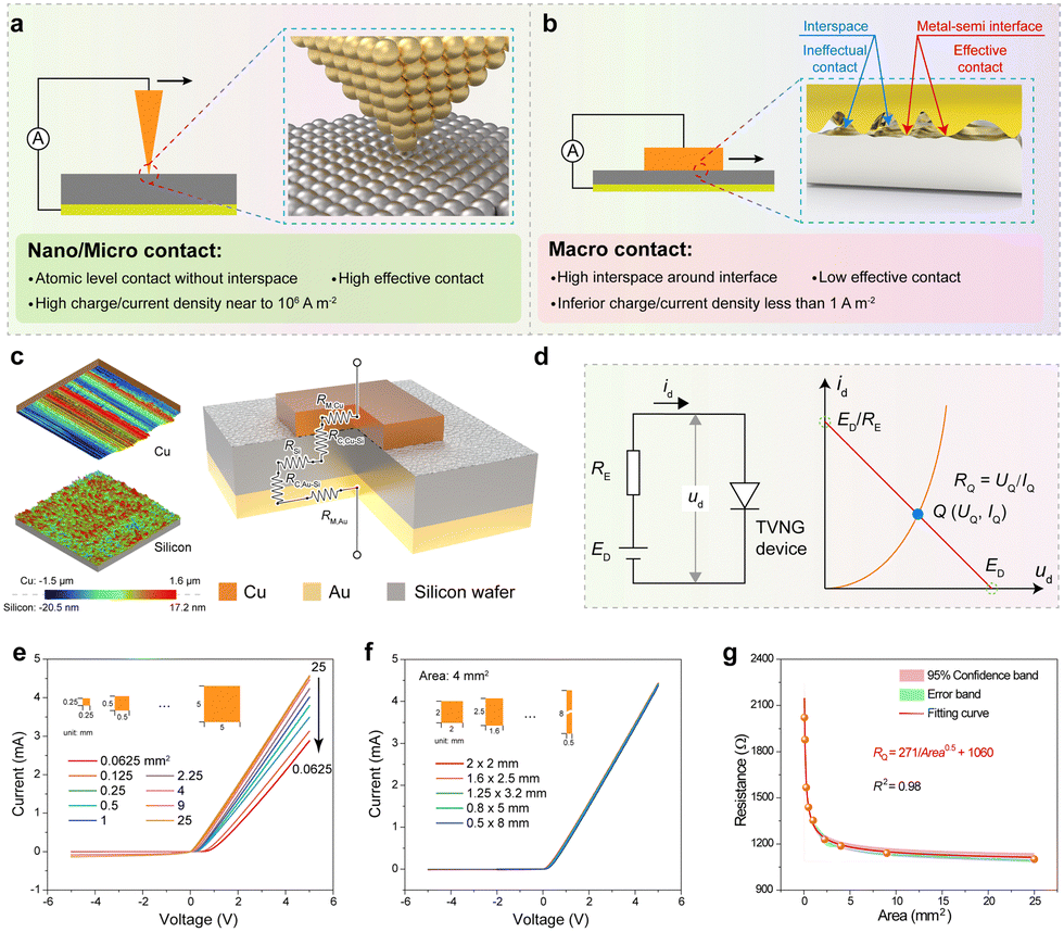
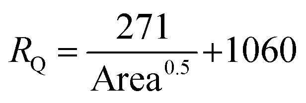
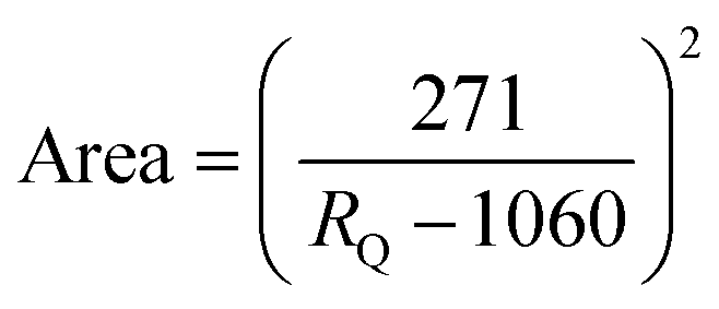
The development of materials and nanotechnology provides more possibilities for the miniaturization and multifunctionality of electronic devices and promotes the construction of large-scale sensor networks for the internet of things in the future.1,2 However, highly decentralized or standalone sensor devices pose new challenges for conventional battery-powered systems, especially in terms of daily maintenance and energy supply issues.3 This is particularly true in fields such as implantable biosensors, wearable electronics, micro robots, and removable environmental sensors.4–6 The emergence of nanogenerators offers a potential solution to address the energy supply issue for distributed sensor systems.7–10Various types of nanogenerators based on different mechanisms were investigated and reported to harvest energy in various forms and convert it into electrical energy, e.g., the triboelectric nanogenerator (TENG) based on triboelectrification,11–14 piezoelectric nanogenerator (PENG) based on piezoelectricity,15–17 and tribovoltaic nanogenerator (TVNG) based on the tribovoltaic effect.18–20 Among them, the TVNG works by creating a new atomic bond at the interface between a p-type and an n-type semiconductor, which releases a quantum of energy called “bindington”, which excites electron–hole pairs located at the PN junction, and the separation of these pairs by the internal built-in electric field generates a flow of direct current.19,20 This process can occur at both the PN semiconductor interface and the Schottky junction interface between the metal and semiconductor, and is often accompanied by very high current densities.18,21 Under the nano/micro contact, due to the very small contact area, the contact condition can even achieve the atom–atom contact at the tip of the atomic force microscope (Fig. 1a), and as a result, the current density can reach an incredible 106 A m−2.18 However, with the scale-up of TVNG devices, the current density of the TVNG greatly decreases to the level of less than 1 A m−2.22–24 This is caused by the inevitable ineffectual contact which was formed by the gaps and voids between the metal and semiconductor (Fig. 1b). Correspondingly, the area of metal–semiconductor contact that can form Schottky contact is very small compared with the ineffectual contact area. Thus, the insufficient contact efficiency causes inferior output performance for large-scale TVNG devices. Therefore, how to quantify the contact efficiency for large-scale TVNG devices and then provide the optimization to improve the effective contact area under large-scale metal-semiconductor contact conditions are very important for enhancing the performance of TVNGs and their practical applications.
 | ||
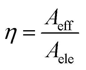
| Fig. 1 Quantification of contact efficiency for TVNGs. (a) Schematic of TVNG under the nano/micro contact. (b) Schematic of the TVNG under the macro contact. (c) Three-dimensional surface topographies of silicon and Cu electrode for the TVNG and schematic diagram of resistance composition in TVNG device. (d) Equivalent circuit diagram to determine the quiescent operation point of the TVNG device. (e) I–V curves of Cu–Si junction with different areas of Cu electrodes. (f) I–V curves of Cu–Si junction with different shapes of Cu electrodes (area: 4 mm2). (g) Standard cure of contact resistance vs. contact area. | ||
In this work, we propose a quantification method to measure the contact efficiency of large-scale TVNGs and present a design optimization strategy to enhance their efficiency. Our results show that the contact efficiency of conventional TVNGs using Cu and p-type silicon under macro contact conditions is only 0.038% (electrode size: 1 cm2), which explains the significant performance gap between large-scale and nano/micro contact TVNGs. Based on the working mechanism of TVNGs, an interface optimization method was proposed, and the contact efficiency of large-scale TVNGs can be successfully improved to 2.45% (loading force: 10 N, electrode size: 1 cm2), which is over 65 times higher than those of conventional devices. Thus, the optimized TVNG also achieved a record-level charge density of 660 mC m−2 and a large energy density of 17.3 mJ m−2 within one operation circle (sliding distance: 1 cm), which is close to 3-times that of the conventional sliding-mode TENG. Moreover, we discovered that the decrease in contact efficiency is the critical issue leading to performance degeneration after long-term operation, but our design optimization approach effectively alleviates this problem. This work not only develops an effective approach for the quantification of large-scale TVNG energy harvesters, providing prerequisites for their performance improvement, but also presents fundamental insights into the mechanism of TVNG devices.
Results and discussion
The TVNG's mechanism relies on electron–hole pair separation via an internal electric field at the junction interface. Essential to output, interface contact profoundly influences the TVNG performance. Fig. S1 (ESI†) illustrates Cu-silicon contact, forming a Schottky junction with varied I–V curves under diverse loading forces. Increased loading boosts current, signifying improved metal–semiconductor contact.23,25,26 Inherent contact resistance27,28 impacts TVNG's forward bias I–V curve and turn-on voltage (Table S1, ESI†), linked to effective contact area. Larger area implies lower contact resistance, benefiting electron flow. Hence, TVNG contact efficiency hinges on Cu-silicon contact resistance and can be determined by the resultant effective contact area (contact resistance is inversely proportional to effective contact area, as discussed in Note S1, ESI†). As shown in Fig. 1c, for the TVNG, the contact surface between the electrode and semiconductor is rough on the atomic level, suggesting that only part of the contact area is effective. Under the contact condition for the TVNG device, its total resistance (RT), except for the external resistance, can be divided into three components: the resistance of the metallic electrodes (Rm,Cu, Rm,Au); the resistance of silicon (Rsi); the contact resistance between metal and silicon (Rc,Cu and Rc,Au). Among them, the contact between Au and silicon forms the Ohmic contact, meanwhile, the area of the sputtered Au electrode has a constant area. Thus, the Rm,Cu, Rm,Au, Rc,Au, and Rsi are the constant values (Rcon), and the total resistance RT can be calculated as:| RT = Rm,Cu + Rm,Au + Rc,Au + Rsi + Rc,Cu = Rcon + Rc,Cu | (1) |
To determine the standard curve of contact resistance vs. contact area, the Cu electrodes with various areas are sputtered onto a clear silicon wafer (the bottom electrode is Au with a size of 45 mm−2). The I–V curves with RE of 1 kΩ are shown in Fig. 1e. As the contact area decreases, the contact resistance increases (Fig. S4 and Table S2, ESI†), while the contact resistances are almost invariable under different shapes of Cu electrodes with the same size (Fig. 1f). Based on the average RQ values in Table S3 (ESI†), the standard curve of contact resistance vs. contact area was determined in Fig. 1g. The error band of RQ almost falls within the 95% confidence interval of the fitting curve, as shown in Fig. 1g. Based on the experimental data, the non-linear relationship between the contact resistance and the effective contact area can be fitted by the following equation:
 | (2) |
 | (3) |
 | (4) |
The contact condition at the junction interface is critical for the contact efficiency of TVNGs, particularly in the formation of solid–solid junction interfaces through the contact of metal and semiconductor materials. For the TVNG based on Cu and p-type Si, the contact condition is quite sensitive to the surface roughness of silicon (Fig. S6–S8 and Note S3, ESI†) while it is not so sensitive to the surface roughness variation of Cu, owing to the pronounced plasticity inherent to the metallic structure. Fig. 2a provides optimization methods for the contact condition of TVNG.29,30 When liquid metal (Ga–In alloy) is added to the interface between Cu and p-type silicon, the linear I–V curve overlaps with the I–V curve of 1 kΩ (Fig. S9, ESI†), and the detailed contact condition with Ga–In addition is discussed in Fig. S10 and Note S4 (ESI†). Adding 5 μL ethanol, pure water, or MoS2 suspension liquid (MoS2 content: 1 wt%) on the interface of TVNG leads to a gradual convergence of their respective I–V curves towards the y-axis, suggesting a reduction of RQ. Based on eqn (2), the corresponding effective contact area gradually increases (Fig. 2b). Compared to the TVNG without interface optimization, the effective contact area of TVNG with MoS2 suspension liquid can reach 1.464 mm2, yielding a substantially improved contact efficiency of 1.464%, representing a remarkable increase by more than 40-fold.
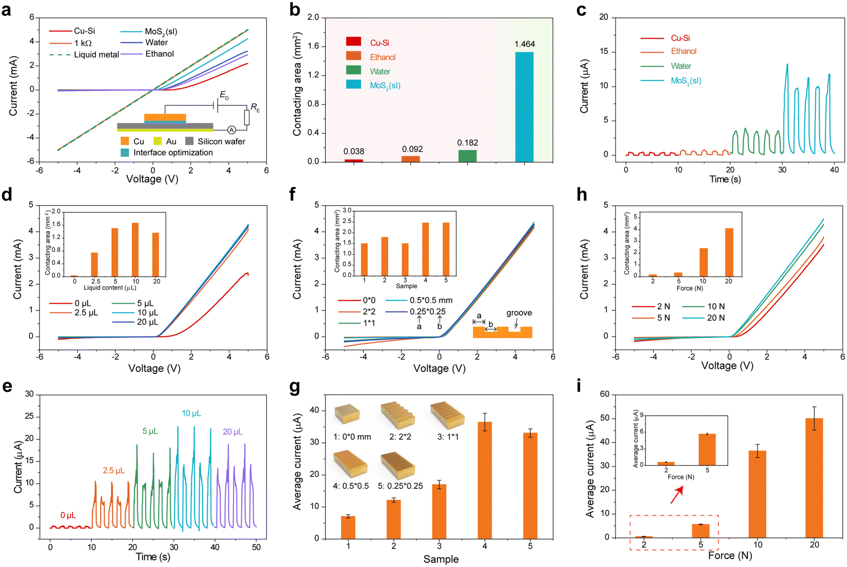 | ||
| Fig. 2 Approaches to improve the contact efficiency for the TVNG. (a) I–V curves, (b) contact area, and (c) short-circuit current of the TVNG with different interface optimization methods (the inset shows the schematic of the circuit, size of Cu electrode: 1 cm2, loading force: 10 N, sliding distance: 1 cm). (d) I–V curves and contact area of the TVNG with different content of MoS2 suspension liquid. (e) Short-circuit current of the TVNG with different content of MoS2 suspension liquid (MoS2 (sl)). (f) I–V curves and contact area of the TVNG with different structures of channeling grooves. (g) Short-circuit current area of the TVNG with different structures of channeling grooves (MoS2 (sl): 5 μL, sliding distance: 1 cm). (h) I–V curves and contact area of the TVNG with different loading forces (channeling groove: 0.5 × 0.5 mm). (i) Short-circuit current area of the TVNG with different loading forces (MoS2 (sl): 5 μL, sliding distance: 1 cm). | ||
Consequently, this leads to an enhancement in the output current of the TVNG, elevating it from 0.36 μA to 12.4 μA (Fig. 2c), along with a corresponding increase in the charge density from 3.1 mC m−2 to 100.0 mC m−2 (calculated by sliding area: 1 cm2). It is notable that this interface optimization extends benefits even to scenarios with significant silicon surface roughness. For instance, at a large silicon roughness of 22.6 nm, contact efficiency improves from 0.021% to 0.51%, as shown in Fig. S11 (ESI†). However, excessive MoS2 suspension liquid diminishes contact efficiency (Fig. 2d). Remarkably, the peak contact area and highest output performance align when 10 μL of MoS2 suspension liquid is applied (Fig. 2e).
To further enhance the effect of interface optimization with MoS2 suspension liquid, microstructural patterns with channelling grooves were introduced onto the device's surface (Fig. 2f and g). This is advantageous in augmenting the contact condition of the TVNG (Fig. S12, ESI†). The width of the microstructural channelling groove ranges from 2 mm to 0.25 mm, and the contact area of the Cu electrode is 1 cm2 (Fig. 2g). Utilizing enhanced liquid wettability via grooved channels, the contact area improves further, and the optimum suspension liquid content is 5 μL (Fig. S13, ESI†). Grooves of 0.25 mm or 0.5 mm yield the TVNG's peak effective contact area of 2.45 mm2 (Fig. 2f, contact efficiency: 2.45%). Meanwhile, the output current of the TVNG with a channelling groove of 0.5 mm surpasses 33 μA (Fig. 2g), along with a charge density of 350 mC m−2.
In addition to these optimization methods, the influence of loading force on the TVNG was also studied. Increasing the loading force from 2 N to 20 N resulted in a rise in the effective contact area of the TVNG from 0.186 mm2 to 4.10 mm2, as shown in Fig. 2h. The output current was increased by 83-fold, from 0.60 μA to 50.1 μA, as depicted in Fig. 2i. It shows a non-linear relationship between the contact area and output current (Note S5, and Fig. S14, ESI†). As shown in Table S4 (ESI†), the contact resistivity (Rc,Cu × Aeff) is different under various loading forces, indicating that the contact conditions vary with the various interface optimizations. For the TVNG without interface optimization (Table S4, ESI†), although it has a smaller effective contact area, its contact resistivity is lower than that of the TVNG with interface optimization under different loading forces because of its pure Schottky contact Cu and p-type silicon.
As mentioned above, by optimizing the interface condition, it is possible to significantly improve the effective contact area and output performance. However, for conventional TVNG devices, the rough surfaces of Cu and silicon can create gaps or voids on the contact surface (Fig. 3a(i)), resulting in areas where Cu–Si Schottky junctions cannot form (the grey part of the projection image in Fig. 3a(i)). These areas do not contribute to the output performance because there is no charge transition (Fig. 3b(i)). The contact area of TVNG can be divided into two parts: as shown in the projection image in Fig. 3a(i), the dark blue area represents the region where carriers can drift from the Cu electrode to the silicon,18 whereas the orange area represents the region where Schottky junctions can form. At the Schottky junctions, atoms from Cu and silicon contact closely with each other, creating a built-in electric field pointing from Cu to silicon (Fig. 3b(ii)). As the Cu electrode slides on the silicon, new chemical bonds are formed, releasing binding energy (known as “bindington”) that excites electron–hole pairs at the contact interface.19,20 The electron–hole pairs separate and expel out of the Schottky junction or barrier at the interface, generating a continuous direct current output in the external circuit (Fig. 3b(ii)).
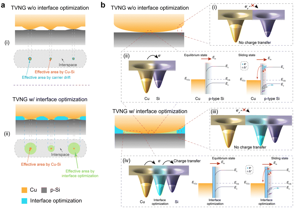 | ||
| Fig. 3 Mechanism of interface optimization for the TVNG. (a) Schematic of the contact condition for the TVNG (i) without and (ii) with interface optimization. (b) Schematic of the charge transfer mechanism for the TVNG under different contact conditions. TVNG without interface optimization: (i) the electron-cloud-potential-well model at the interspace area; (ii) the electron-cloud-potential-well model of the electron transition process and energy band diagram of Cu and p-type silicon. The TVNG with interface optimization: (iii) the electron-cloud-potential-well model at the interspace area; (iv) the electron-cloud-potential-well model of the electron transition process and energy band diagram of Cu and p-type silicon after interface optimization. | ||
The TVNG with interface optimization fills the gaps or voids with MoS2 suspension liquid, creating a Cu–liquid–Si contact around the Cu–Si Schottky junctions. The friction between MoS2 and Cu/silicon, and the friction between liquid and Cu/silicon, have a very weak contribution to the huge output improvement of TVNG with MoS2 (sl) (Fig. S15 and Note S6, ESI†). Since the contact surface has a certain curvature at the microscopic level, the excited carriers can also drift from the Cu electrode to the silicon through the suspension liquid within a certain thickness. Moreover, the TVNG with interface optimization has a larger threshold thickness that can allow carriers to drift due to the larger conductivity (Fig. S16, ESI†) of MoS2 suspension liquid compared to air (as the schematic in Fig. 3b(iv)) or the other interface liquid (the output current in Fig. 2c), while the resistance of the liquid also inevitably increases the contact resistivity (Table S4, ESI†). As a result, the interface optimization method can significantly improve the effective area, depicted by the green part of the projection image in Fig. 3a(ii). However, there are still some useless areas where charge transition cannot occur because the liquid thickness is too large (Fig. 3b(iii)), which is also the reason that excess suspension does not improve performance further (Fig. 2h). In general, interface optimization using MoS2 suspension liquid can significantly improve the effective contact area and output performance of TVNG devices. This is achieved by filling gaps or voids on the contact surface, creating Cu–liquid–Si contacts, and allowing for greater carrier drift, ultimately resulting in enhanced device efficiency.
To enhance the contact efficiency of TVNGs based on the improved approaches and mechanisms, and achieve high-performance devices, a design optimization strategy is proposed (Fig. S17, ESI†). Using these approaches (Note S7, ESI†), we successfully prepared an optimized TVNG (O-TVNG) device (Fig. 4a) made of Cu and p-type silicon, with a channelling groove of width 0.5 mm (the contact area of the Cu electrode is 1 cm2). A 5 μL MoS2 suspension liquid was used as interface optimization. The contact efficiency of O-TVNG can reach 2.45%, which greatly exceeds that of non-optimized TVNG (0.131%, Fig. S18, ESI†). As the sliding velocity increases from 0.01 to 0.08 m s−1, the short-circuit current of the O-TVNG rises from 0.04 mA to 0.8 mA (sliding distance: 1 cm, Fig. 4b), along with transferred charges (current integration) from 36 μC to 47 μC (Fig. S19, ESI†). Under different accelerated speeds, the O-TVNG achieves a high peak short-circuit current of 2.3 mA (Fig. 4c), with transferred charge density reaching 660 mC m−2 (Fig. S20 and S21, ESI†). In contrast, the non-optimized TVNG only has an inferior current of 13 μA and a charge density of 5.5 mC m−2 under identical test conditions (Fig. S22, ESI†).
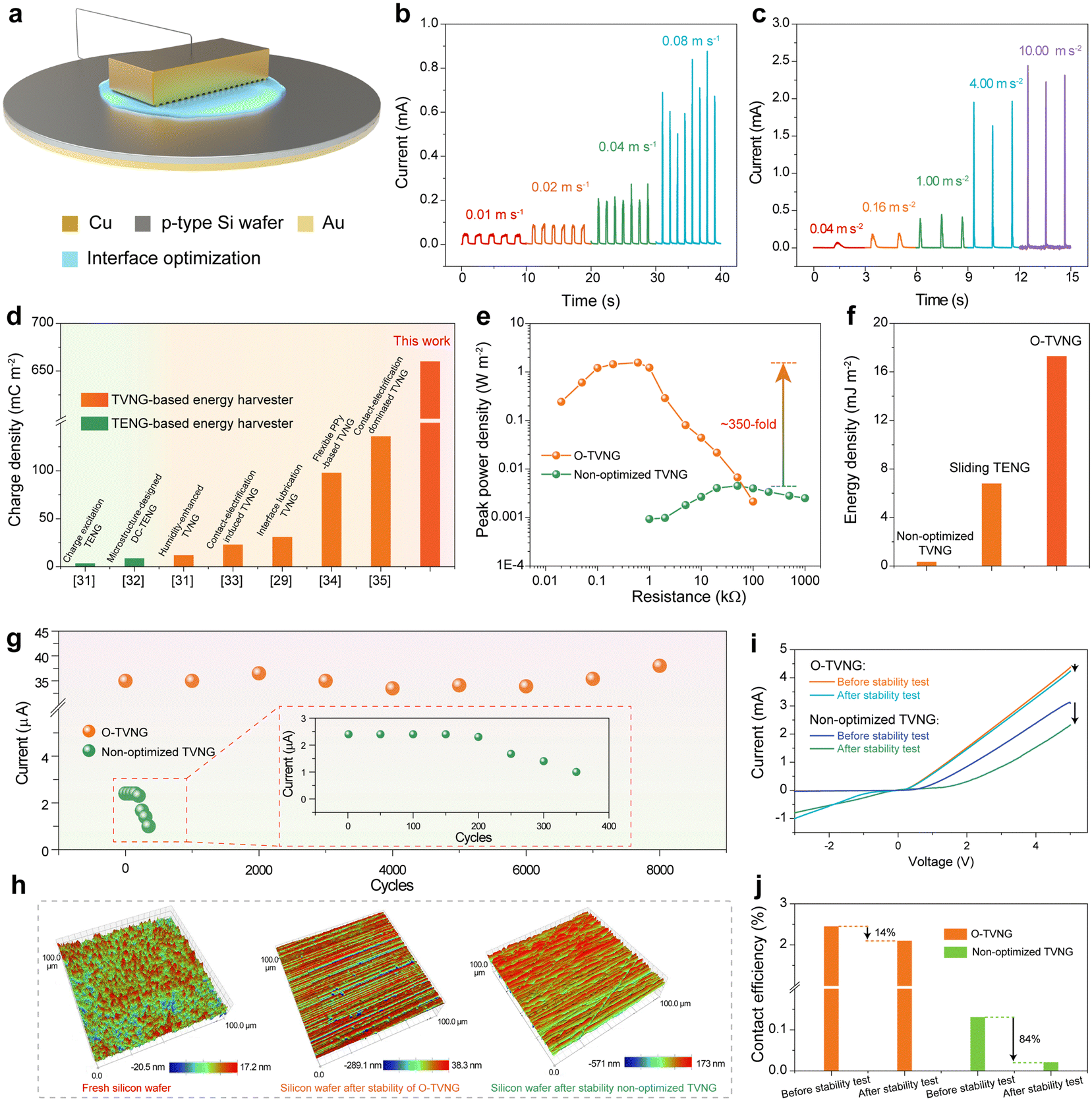 | ||
| Fig. 4 Design optimization and enhanced performance of the TVNG. (a) Schematic of the O-TVNG device. The short-circuit current of the O-TVNG device (b) under different sliding velocities and (c) different sliding accelerations (sliding distance: 1 cm). (d) Comparison of the charge density of TENG- and TVNG-based energy harvesters.29–35 (e) Peak power density of the O-TVNG and non-optimized TVNG (sliding distance: 1 cm, acceleration: 10 m s−2). (f) Energy density within 1 operation cycle of the TVNG and TENG at matched impedance. (g) Short-circuit current stability under the long-term operation of O-TVNG and non-optimized TVNG devices. (h) Three-dimensional surface topographies of silicon wafers for the TVNG before/after the stability test. (i) I–V curves of the TVNG before/after the stability test, and (j) corresponds to the contact efficiency. | ||
The high charge density of the O-TVNG greatly exceeds that of the TENG-based energy harvester (maximum value: 4.13 mC m−2 for an alternating current TENG and 8.8 mC m−2 for a direct current TENG).31,32 It also increases by 4-fold compared to the state-of-the-art value in a TVNG-based energy harvester (maximum value: 136 mC m−2),29,30,33–35 as shown in Fig. 4. Taking advantage of the high output performance and low contact resistance, the O-TVNG device achieves a peak power density of 1.56 W m−2 under an external resistance of 0.6 kΩ (Fig. 4e, accelerated speed: 10 m s−2), which increases by 350-fold compared to that of non-optimized TVNG (0.0045 W m−2 under 50 kΩ). In addition, Fig. 4f shows the energy density near their matched impedance, and the corresponding V–Q curves and analyses are shown in Fig. S23 and S24 and Note S7 (ESI†). The O-TVNG achieves an extremely high charge density, improving its energy density to 17.3 mJ m−2 under a relatively low voltage.
To enhance the practicality of TVNGs, the consideration of performance stability is imperative, given the solid–solid friction involved. Fig. 4g suggests the output performance of the non-optimized TVNG begins to decline after 200 operation cycles, while the O-TVNG maintains its stable output after 8000 cycles. Scanning electron microscopy images reveal that the O-TVNG produces fewer scratches due to friction wear (Fig. 4h and Fig. S25, ESI†). According to the I–V curves (Fig. 4i), despite the rectifier characteristics of Cu and p-type silicon junction being reduced after a long-term operation, the O-TVNG device has a smaller RQ. The contact efficiency of the O-TVNG only slightly decreases to 2.10% compared to that of the fresh one (2.45%), while the non-optimized TVNG's contact efficiency significantly declines from 0.131% to 0.021% (Fig. 4j). The interface optimization strategy also provides excellent protection for the silicon surface during the working process, which maintains the surface characteristics of silicon (as shown by the analyses of X-ray diffraction and X-ray photoelectron spectroscopy results in Fig. S26–S28 and Note S8, ESI†). These results demonstrate the effectiveness of the design optimization approach in improving the comprehensive performance of TVNG devices.
Conclusions
In summary, we have developed a method to quantify the contact efficiency for large-scale TVNG devices and proposed a contact interface optimization strategy, including surface roughness control, interface lubrication, and microstructural pattern design on electrodes, to enhance their performance. Taking advantage of this quantification method, we have found that the contact efficiency of conventional TENG devices based on Cu and p-type silicon is only 0.038% under macro contact conditions, indicating that only a small fraction of the large electrode contributes to the output performance. This explains the significant performance gap between large-scale and nano/micro contact TENG devices. Moreover, our design optimization approach and corresponding mechanism have effectively improved the contact efficiency of large-scale TENG devices to over 65-fold. Consequently, the optimized TENG device can achieve a large short-circuit current of 23 A m−2, along with a record-level charge density of 660 mC m−2 and a high energy density of 17.3 mJ m−2 within 1 cm sliding distance. Furthermore, we have identified the decrease in contact efficiency as the primary cause of performance degeneration after long-term operation, and it can be effectively alleviated using the interface optimization approaches. These results demonstrate that the interface optimization approach not only increases the output performance but also the stability of TVNGs, providing practical and fundamental insights for real-world applications. In summary, our study establishes the prerequisites for achieving high performance in large-scale TENG energy harvesters and provides valuable guidance for the design of such devices.Author contributions
Zhihao Zhao: conceptualization, methodology, validation, formal analysis, investigation, data curation, writing – original draft, and visualization. Jiayue Zhang: writing – review & editing, validation, and visualization. Wenyan Qiao: investigation and methodology. Linglin Zhou, Ziting Guo, and Xinyuan Li: methodology. Zhong Lin Wang: conceptualization, writing – review & editing, and supervision. Jie Wang: conceptualization, writing – review & editing, and supervision.Conflicts of interest
There are no conflicts to declare.Acknowledgements
The authors acknowledge the financial support from the National Key R & D Project from Ministry of Science and Technology, China (2021YFA1201602), the National Nature Science Foundation of China (52302214, U21A20147), the Fundamental Research Funds for the Central Universities (E1E46802 and E2E46803), and the China Postdoctoral Science Foundation (2021M703171).Notes and references
- L. Portilla, K. Loganathan, H. Faber, A. Eid, J. G. D. Hester, M. M. Tentzeris, M. Fattori, E. Cantatore, C. Jiang, A. Nathan, G. Fiori, T. Ibn-Mohammed, T. D. Anthopoulos and V. Pecunia, Nat. Electron., 2023, 6, 10–17 Search PubMed.
- D. C. Nguyen, M. Ding, P. N. Pathirana, A. Seneviratne, J. Li, D. Niyato, O. Dobre and H. V. Poor, IEEE Internet Things J., 2022, 9, 359–383 Search PubMed.
- X. Zhao, H. Askari and J. Chen, Joule, 2021, 5, 1391–1431 CrossRef.
- W. Gao, S. Emaminejad, H. Y. Y. Nyein, S. Challa, K. Chen, A. Peck, H. M. Fahad, H. Ota, H. Shiraki, D. Kiriya, D.-H. Lien, G. A. Brooks, R. W. Davis and A. Javey, Nature, 2016, 529, 509–514 CrossRef CAS PubMed.
- G. Conta, A. Libanori, T. Tat, G. Chen and J. Chen, Adv. Mater., 2021, 33, 2007502 CrossRef CAS PubMed.
- M. Wang, Y. Yang, J. Min, Y. Song, J. Tu, D. Mukasa, C. Ye, C. Xu, N. Heflin, J. S. McCune, T. K. Hsiai, Z. Li and W. Gao, Nat. Biomed. Eng., 2022, 6, 1225–1235 CrossRef CAS PubMed.
- H. Guo, X. Pu, J. Chen, Y. Meng, M.-H. Yeh, G. Liu, Q. Tang, B. Chen, D. Liu, S. Qi, C. Wu, C. Hu, J. Wang and Z. L. Wang, Sci. Rob., 2018, 3, eaat2516 CrossRef PubMed.
- J. Xiong, P. Cui, X. Chen, J. Wang, K. Parida, M.-F. Lin and P. S. Lee, Nat. Commun., 2018, 9, 4280 CrossRef PubMed.
- W. Wang, J. Pang, J. Su, F. Li, Q. Li, X. Wang, J. Wang, B. Ibarlucea, X. Liu, Y. Li, W. Zhou, K. Wang, Q. Han, L. Liu, R. Zang, M. H. Rümmeli, Y. Li, H. Liu, H. Hu and G. Cuniberti, InfoMat, 2022, 4, e12262 CrossRef.
- H. Ryu, H.-M. Park, M.-K. Kim, B. Kim, H. S. Myoung, T. Y. Kim, H.-J. Yoon, S. S. Kwak, J. Kim, T. H. Hwang, E.-K. Choi and S.-W. Kim, Nat. Commun., 2021, 12, 4374 CrossRef CAS PubMed.
- F.-R. Fan, Z.-Q. Tian and Z. Lin Wang, Nano Energy, 2012, 1, 328–334 CrossRef CAS.
- J. Wang, C. Wu, Y. Dai, Z. Zhao, A. Wang, T. Zhang and Z. L. Wang, Nat. Commun., 2017, 8, 88 CrossRef PubMed.
- Z. Zhao, Y. Dai, D. Liu, L. Zhou, S. Li, Z. L. Wang and J. Wang, Nat. Commun., 2020, 11, 6186 CrossRef CAS PubMed.
- R. Hinchet, H.-J. Yoon, H. Ryu, M.-K. Kim, E.-K. Choi, D.-S. Kim and S.-W. Kim, Science, 2019, 365, 491–494 CrossRef CAS PubMed.
- S. Xu, Y. Qin, C. Xu, Y. Wei, R. Yang and Z. L. Wang, Nat. Nanotechnol., 2010, 5, 366–373 CrossRef CAS PubMed.
- H. Wu, Y. Huang, F. Xu, Y. Duan and Z. Yin, Adv. Mater., 2016, 28, 9881–9919 CrossRef CAS PubMed.
- W. Deng, Y. Zhou, A. Libanori, G. Chen, W. Yang and J. Chen, Chem. Soc. Rev., 2022, 51, 3380–3435 RSC.
- J. Liu, A. Goswami, K. Jiang, F. Khan, S. Kim, R. McGee, Z. Li, Z. Hu, J. Lee and T. Thundat, Nat. Nanotechnol., 2018, 13, 112–116 CrossRef CAS PubMed.
- C. Xu, J. Yu, Z. Huo, Y. Wang, Q. Sun and Z. L. Wang, Energy Environ. Sci., 2023, 16, 983–1006 RSC.
- M. Zheng, S. Lin, Z. Tang, Y. Feng and Z. L. Wang, Nano Energy, 2021, 83, 105810 CrossRef CAS.
- X. Huang, X. Xiang, J. Nie, D. Peng, F. Yang, Z. Wu, H. Jiang, Z. Xu and Q. Zheng, Nat. Commun., 2021, 12, 2268 CrossRef CAS PubMed.
- J. Liu, F. Liu, R. Bao, K. Jiang, F. Khan, Z. Li, H. Peng, J. Chen, A. Alodhayb and T. Thundat, ACS Appl. Mater. Interfaces, 2019, 11, 35404–35409 CrossRef CAS PubMed.
- Z. Zhang, D. Jiang, J. Zhao, G. Liu, T. Bu, C. Zhang and Z. L. Wang, Adv. Energy Mater., 2020, 10, 1903713 CrossRef CAS.
- C. Ma, B. Kim, S.-W. Kim and N.-G. Park, Energy Environ. Sci., 2021, 14, 374–381 RSC.
- X. Luo, L. Liu, Y.-C. Wang, J. Li, A. Berbille, L. Zhu and Z. L. Wang, Adv. Funct. Mater., 2022, 32, 2113149 CrossRef CAS.
- M. Zheng, S. Lin, L. Xu, L. Zhu and Z. L. Wang, Adv. Mater., 2020, 32, 2000928 CrossRef CAS PubMed.
- P.-C. Shen, C. Su, Y. Lin, A.-S. Chou, C.-C. Cheng, J.-H. Park, M.-H. Chiu, A.-Y. Lu, H.-L. Tang, M. M. Tavakoli, G. Pitner, X. Ji, Z. Cai, N. Mao, J. Wang, V. Tung, J. Li, J. Bokor, A. Zettl, C.-I. Wu, T. Palacios, L.-J. Li and J. Kong, Nature, 2021, 593, 211–217 CrossRef CAS PubMed.
- X. Zhang, Z. Kang, L. Gao, B. Liu, H. Yu, Q. Liao, Z. Zhang and Y. Zhang, Adv. Mater., 2021, 33, 2104935 CrossRef CAS PubMed.
- W. Qiao, Z. Zhao, L. Zhou, D. Liu, S. Li, P. Yang, X. Li, J. Liu, J. Wang and Z. L. Wang, Adv. Funct. Mater., 2022, 32, 2208544 CrossRef CAS.
- Z. Wang, L. Gong, S. Dong, B. Fan, Y. Feng, Z. Zhang and C. Zhang, J. Mater. Chem. A, 2022, 10, 25230–25237 RSC.
- H. Wu, J. Wang, W. He, C. Shan, S. Fu, G. Li, Q. Zhao, W. Liu and C. Hu, Energy Environ. Sci., 2023, 16, 2274–2283 RSC.
- Z. Zhao, L. Zhou, S. Li, D. Liu, Y. Li, Y. Gao, Y. Liu, Y. Dai, J. Wang and Z. L. Wang, Nat. Commun., 2021, 12, 4686 CrossRef CAS PubMed.
- Z. Wang, Z. Zhang, Y. Chen, L. Gong, S. Dong, H. Zhou, Y. Lin, Y. Lv, G. Liu and C. Zhang, Energy Environ. Sci., 2022, 15, 2366–2373 RSC.
- J. Meng, C. Pan, L. Li, Z. H. Guo, F. Xu, L. Jia, Z. L. Wang and X. Pu, Energy Environ. Sci., 2022, 15, 5159–5167 RSC.
- Z. Zhang, Z. Wang, Y. Chen, Y. Feng, S. Dong, H. Zhou, Z. L. Wang and C. Zhang, Adv. Mater., 2022, 34, 2200146 CrossRef CAS PubMed.
Footnotes |
| † Electronic supplementary information (ESI) available: Additional experimental description of device fabrication, characterization and electrical measurement of the TVNG, and supplementary figures, supplementary tables and supplementary notes. See DOI: https://doi.org/10.1039/d3mh01369c |
| ‡ These authors contributed equally to this work. |
| This journal is © The Royal Society of Chemistry 2023 |