
Metallene-related materials for electrocatalysis and energy conversion
Minghao
Xie
,
Sishuang
Tang
 ,
Bowen
Zhang
and
Guihua
Yu
*
,
Bowen
Zhang
and
Guihua
Yu
*
Materials Science and Engineering Program and Walker Department of Mechanical Engineering, The University of Texas at Austin, Austin, TX 78712, USA. E-mail: ghyu@austin.utexas.edu
First published on 7th December 2022
Abstract
As a member of graphene analogs, metallenes are a class of two-dimensional materials with atomic thickness and well-controlled surface atomic arrangement made of metals or alloys. When utilized as catalysts, metallenes exhibit distinctive physicochemical properties endowed from the under-coordinated metal atoms on the surface, making them highly competitive candidates for energy-related electrocatalysis and energy conversion systems. Significantly, their catalytic activity can be precisely tuned through the chemical modification of their surface and subsurface atoms for efficient catalyst engineering. This minireview summarizes the recent progress in the synthesis and characterization of metallenes, together with their use as electrocatalysts toward reactions for energy conversion. In the Synthesis section, we pay particular attention to the strategies designed to tune their exposed facets, composition, and surface strain, as well as the porosity/cavity, defects, and crystallinity on the surface. We then discuss the electrocatalytic properties of metallenes in terms of oxygen reduction, hydrogen evolution, alcohol and acid oxidation, carbon dioxide reduction, and nitrogen reduction reaction, with a small extension regarding photocatalysis. At the end, we offer perspectives on the challenges and opportunities with respect to the synthesis, characterization, modeling, and application of metallenes.
 Minghao Xie | Minghao Xie received his BS degree in Materials Chemistry from Sichuan University in 2015 and MS in Materials Science from Carnegie Mellon University in 2016. He then received his PhD degree in Chemistry and Biochemistry from the Georgia Institute of Technology in 2021. Since 2021, he has been a postdoctoral fellow in Prof. Guihua Yu's group at The University of Texas at Austin. His research focuses on the controlled synthesis of two-dimensional metal nanomaterials for applications in energy and catalytic processes. |
 Sishuang Tang | Sishuang Tang received her BS degree in Chemistry from New York University in 2020. She is pursuing her PhD degree in Materials Science and Engineering at The University of Texas at Austin under the supervision of Prof. Guihua Yu. Her current research interest includes structural engineering of transition metal-based electrocatalysts for ammonia synthesis. |
 Bowen Zhang | Bowen Zhang received his BS degree from Henan University in 2005 and PhD from the Lanzhou Institute of Chemical Physics, Chinese Academy of Science in 2014, both in Materials Science. He is currently a visiting scholar in Prof. Guihua Yu's group at The University of Texas at Austin. His research focuses on the design and development of MXene-based nanomaterials for applications in electrochemical systems and battery technologies. |
 Guihua Yu | Guihua Yu received his BS degree with the highest honor from the University of Science and Technology of China in 2003, and his PhD from Harvard University in 2009. Currently, he is a Temple Foundation Endowed Professor of Materials Science and Mechanical Engineering at The University of Texas at Austin. His research interests include rational design and synthesis of functional organic and hybrid organic–inorganic nanomaterials, fundamental understanding of their chemical and physical properties, and development of large-scale assembly and integration methodologies to enable various important technologies in energy, environment and sustainability. |
1. Introduction
Materials with an ultrathin two-dimensional (2D) structure exhibit unique and unprecedented chemical, electronic, and catalytic properties owing to the distinctive electron confinement featured in two dimensions which is unachievable either in other classes of nanomaterials or their bulk counterparts.1–7 Since the exfoliation of the first 2D nanocrystal, graphene, the family of 2D materials has experienced a big boom. As a remarkable group of 2D materials, graphene analogs characterized by atomic layers are essentially important for surface-related applications due to their ultrahigh surface-to-volume ratio and thus maximized atomic utilization efficiency (AUE). To date, the reported graphene analogs are essentially divided into three categories (Fig. 1A): (1) metal-free analogs such as carbon nitride, boron nitride, phosphorene, etc.; (2) transition metal compounds such as carbides (also known as MXenes), chalcogenide, hydroxide, etc.; (3) metallic materials such as monometallenes, bimetallenes, and trimetallenes, etc. Featured with laminar structures stacked by van der Waals forces, the first two categories can be synthesized via top-down exfoliation or bottom-up growth down to single atomic layers.8 In contrast, due to the robust and isotropic nature of metallic bonds, the majority of metal materials are characterized by closely packed crystal structures, making their atomically thin morphology thermodynamically unfavorable.9 As such, the preparation of metallenes remains a significant challenge, hindering their generation for potential applications in the past few decades.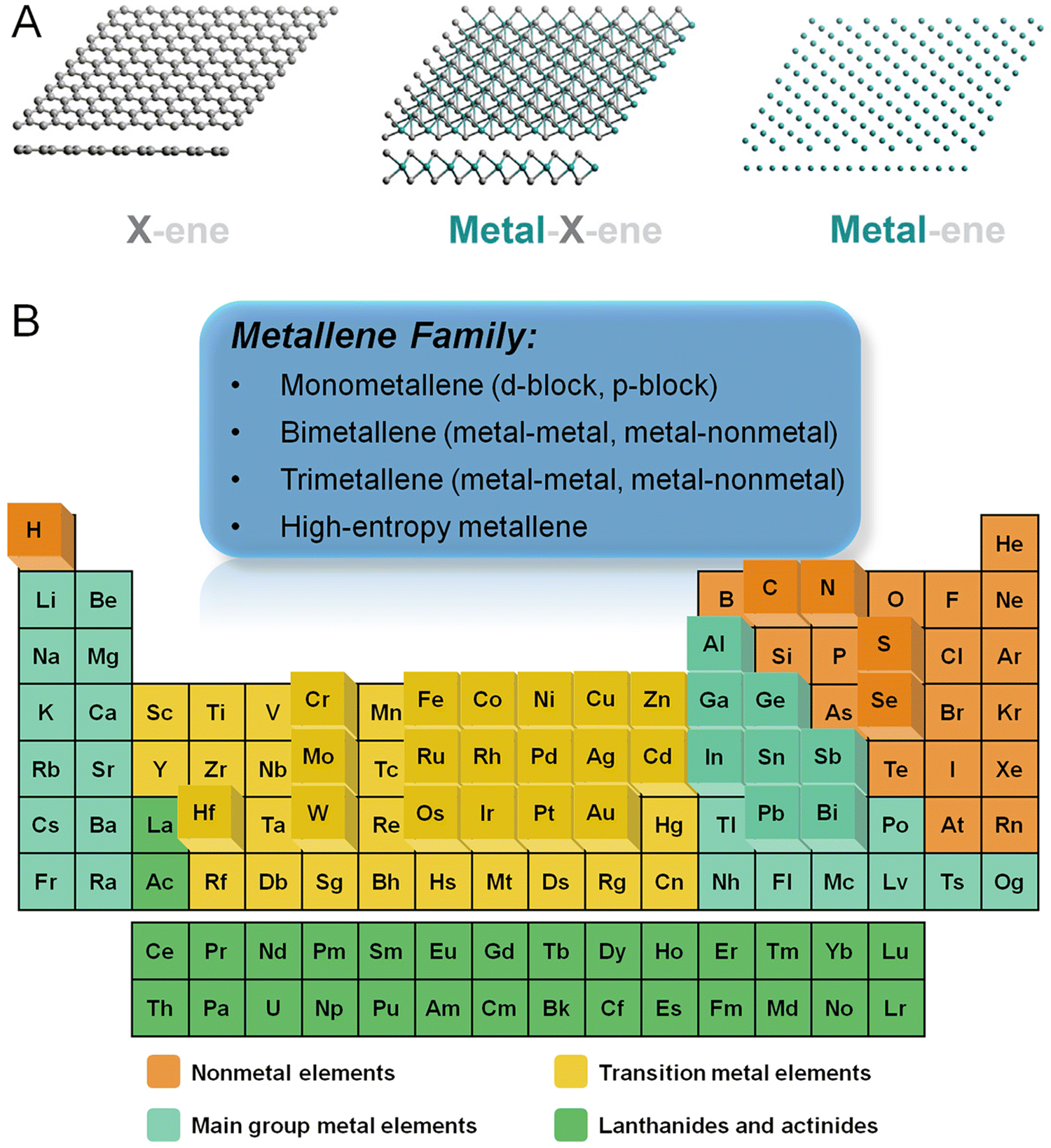 | ||
| Fig. 1 (A) Schematic illustration showing three-generational development of 2D atomically thin materials including metal-free (X-ene, X = B, C, N, P, etc.), transition metal compounds (metal-X-ene, X = C, N, O, S, etc.), and metallic materials (metal-ene). (B) Overview of the elements involved in metallenes in the periodic table achieved by either experiments or theoretical calculations. (A) Reproduced from ref. 8 with permeation from CellPress. Copyright 2019. | ||
As a newcomer of 2D materials, metallenes have garnered ever-increasing attention in recent years owing to their unique superiorities including the maximized exposure of active metal sites and high conductivity for catalysis, electronics, and energy-related applications.10,11 Particularly, the precisely tunable electronic structure, modifiable surface state, and high carrier mobility make metallenes competitive candidates for energy conversion devices. In essence, metallenes refer to a class of atomically thin 2D materials composed of metals and alloys. Fig. 1B instinctively demonstrates an overview of the classification of metallenes from the perspective of compositions and the metal elements reported so far. Metallenes composed of noble metals like Pd,12,13 Ir,14 and Rh15,16 which are commonly used in electrocatalysis for energy conversion delivered outstanding electrocatalytic performance for practical applications. In addition, several strategies were developed to boost their performance to a new limit, including atomic doping, lattice engineering, surface modification, etc.10 On top of that, the recent success of PdMo bimetallene with four atomic layers significantly proved the superior performance of metallenes in electrocatalysis of oxygen reduction, triggering substantial studies of metallenes as electrocatalysts for energy-related applications.17
In this minireview, we summarize some of the recent advancements and achievements in the fabrication, characterization, and electrocatalytic applications of metallenes. We begin with a brief introduction to general approaches to the synthesis and characterization of metallenes. We pay particular attention to the design principles of metallenes from the viewpoint of catalyst engineering with high performance. We then discuss the electrocatalytic properties of metallenes and showcase a set of energy-related reactions including oxygen reduction, hydrogen evolution, alcohol and acid oxidation, carbon dioxide reduction, and nitrogen reduction reaction, with extended discussion regarding photocatalysis. Finally, on the basis of the present progress, we highlight some potential prospects on the challenges and outlooks with respect to synthesis, characterization, modeling, and stability of metallenes for realistic energy application.
2. Definition, synthesis, and characterization of metallenes
The definition of metallene is adopted from that of graphene. In principle, a well-defined metallene refers to a single atomic layer composed of metal atoms. Similar to graphene, the monolayer structure is highly flexible which can feature atomical surface flatness when deposited on a substrate or surface curvature when it is freestanding due to the high surface free energy. The use of “ene” for metal is also due to the comparable electronic properties between metallenes and graphene when the thickness of metal is reduced to a monolayer.8 In reality, the high energy barrier to overcome and the thermodynamic instability of metal monolayers limits the synthesis approaches for obtaining this type of nanostructure either on a substrate or in an isolated state.11 In this Minireview, the definition of metallenes generally relates to atomically thin 2D metals with a thickness of around 1 nm (corresponding to atomic layers) with rare exceptions above 2 nm. Different from conventional 2D metal nanoplates typically with flat surface morphology, metallenes feature a lower thickness and much larger lateral size, which makes them favorable to form highly curved morphology in most cases.2.1. Synthesis of metallene: bottom-up, top-down, and topotactic metallization
The controlled synthesis of metallene enables the alteration of thickness, composition, and crystal structure to vary their electrochemical properties and thus catalytic performance. Thanks to the efforts of many groups, a number of approaches have been developed for the synthesis of 2D metal nanomaterials with controlled thickness, composition, and crystal structure.9–11,18,19 The typical synthesis methods for metallene are summarized in Table 1, which can be generally categorized into three major strategies including bottom-up wet-chemical methods, top-down exfoliation methods, and topotactic metallization approaches.| Synthesis approaches | Metals | Thickness | Applications | Ref. | |
|---|---|---|---|---|---|
| Bottom-up | Ligand-confined growth | Pd | 5 layers | CO2RR | 20 |
| 3–8 layers | ORR | 13 | |||
| 0.8 nm | Glycerol oxidation | 21 | |||
| 0.9 nm | ORR | 12 | |||
| Rh | 0.4 nm | Hydrogenation | 15 | ||
| ∼1.0 nm | Hydrogenation | 16 | |||
| Co | 0.84 nm | CO2RR | 22 | ||
| RuRh | 0.83 nm | HER | 23 | ||
| PdMo | 0.88 nm | ORR | 17 | ||
| PdIr | 1.0 nm | HER, FAOR | 24 | ||
| PdFe1 | 0.8–1 nm | NRR | 25 | ||
| RhPd-H | ∼7 layers | HER | 26 | ||
| PtPdM (M = Fe, Co, Ni) | 1.4 nm | ORR, EGOR, EOR | 27 | ||
| Space-confined growth | PdCo | Monolayer | ORR | 28 | |
| Pt | Monolayer | ORR | 29 | ||
| Template-directed growth | Fe | Monolayer | — | 30 | |
| Au | ∼2.4 nm | — | 31 | ||
| HEA | 0.8 nm | ORR | 32 | ||
| Top-down | Liquid-phase exfoliation | Bi | 1.2–1.5 nm | CO2RR | 33 |
| Sb | Monolayer | Perovskite solar cells | 34 | ||
| 1.5 nm | HER | 35 | |||
| Co | 1.3 nm | CO2RR | 36 | ||
| Mechanical exfoliation | Sb | Monolayer | Perovskite solar cells | 37 | |
| Solid-melt exfoliation | Ga | ∼4 nm | — | 38 | |
| Electron beam dealloying | Au | Monolayer | — | 39 | |
| Topotactic metallization | Chemical metallization | Bi | 0.65 nm | CO2RR | 40 |
| Rh | 1.0–1.1 nm | NRR | 41 | ||
| NiFe | 0.65 nm | NRR | 42 | ||
| Electrochemical metallization | Bi | 1.28–1.45 nm | CO2RR | 43 | |
| 1.23 nm | CO2RR | 44 | |||
| 1.21–1.55 nm | CO2RR | 45 | |||
| 1.02 nm | CO2RR | 46 | |||
In the bottom-up methods, the major concern for the generation of metallene is the introduction of anisotropic growth of metal at the nanoscale. According to the classic LaMer model, the anisotropic nucleation of metal atoms for the birth of 2D nuclei is critical to induce the subsequent production of an ultrathin nanostructure of metal. To confine the thickness of the 2D nanostructure, the growth perpendicular to the basal planes of the nanostructure needs to be passive, which can be achieved by well-selected ligands preferentially attached to the basal planes to make this ultrathin nanostructure thermodynamically favorable. As demonstrated in Fig. 2A and B, the ligands used for anisotropic confinement can be inorganic molecules such as CO or organic surfactants to produce ultrathin Pd metallenes.10,20,21 Similar to ligand-confined growth, the anisotropy can also be induced by laminar structures in which the growth of metals is well-confined within the interlayer space of the layered structures. As shown in Fig. 2C, the PdCo single atomic layers can be obtained by a space-confined growth of PdCo monolayers in the angstrom-sized interlamination of layered crystalline clay mineral montmorillonite.28 In addition to the confined growth approaches, the 2D nanostructure can be thermodynamically favored by template-mediated anisotropy. Starting from a template with an atomically flat 2D surface, metal atoms can be preferentially deposited on the surface of the template for the generation of ultrathin metallic layers. As an intuitively selected template, graphene has been used for the preparation of metallenes. As reported by Zhang and coworkers, Au metallene with an unconventional hexagonal close packed (hcp) crystal structure can be obtained by depositing Au atoms on graphene.31 It is worth noting that the thermodynamically unfavored metallene can also be stabilized in the pores of graphene, by which the free-standing Fe monolayer suspended in graphene pores was gained.30 Besides graphene, metallic templates are also widely used for the epitaxial growth of metal atoms by atomic layer-by-layer deposition. By using this strategy, a variety of metal atoms can be deposited on the surface of templates in a well-controlled way, which paves the way for the formation of metallene with higher complexity in terms of composition. For example, Guo and coworkers reported metallene composed of high-entropy alloys via galvanic replacement reaction and co-reduction of various metal ions on the surface of an Ag template followed by selective etching of the template.32 Beyond the aforementioned methods, metallene can also be synthesized via other unique bottom-up approaches including pulsed laser deposition, pyrolysis, electrodeposition, and photoreduction, etc.11
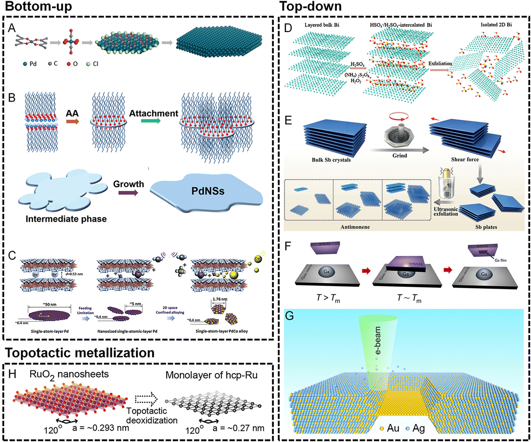 | ||
| Fig. 2 Synthesis techniques for metallenes. (A–C) Bottom-up approaches. (A) Schematic showing the synthesis mechanism of hexagonal Pd metallene by CO molecule-confined growth. Reproduced from ref. 20 with permission from Wiley-VCH. Copyright 2018. (B) Schematic illustration of the formation of Pd metallene by organic ligand-confined growth. Reproduced from ref. 21 with permission from the Royal Society of Chemistry. Copyright 2017. (C) Schematic illustrations of the synthesis of a Pd–Co monolayer by space-confined growth. Reproduced from ref. 28 with permission from Elsevier. Copyright 2020. (D–G) Top-down approaches. (D) Schematic of the H2SO4-assisted liquid exfoliation of bulk Bi into metallene. Reproduced from ref. 50 with permission from the Royal Society of Chemistry. Copyright 2018. (E) Schematic illustrations of the preparation of antimonene by grinding bulk Sb crystals into Sb plates followed by exfoliating the Sb plates into antimonene. Reproduced from ref. 37 with permission from Wiley-VCH. Copyright 2018. (F) Schematic of the solid-melt exfoliation technique to produce gallenene on the surface of Si/SiO2 substrates. Reproduced from ref. 38 with permission from AAAS. Copyright 2018. (G) Schematic of the fabrication of an Au monolayer by in situ electron beam-induced dealloying of an Au–Ag alloy. Reproduced from ref. 39 with permission from American Chemical Society. Copyright 2019. Topotactic metallization approaches. (H) Schematic of topological metallization of exfoliated RuO2 nanosheets to prepare the Ru monolayer. Reproduced from ref. 51 with permission from American Chemical Society. Copyright 2013. | ||
It is well known that laminar materials such as graphite, transition metal dichalcogenides, and layered double hydroxides feature strong in-plane covalent bonds and weak interlayer van der Waals interactions, providing possibility to exfoliate them into mono- or few layers.47–49 Likewise, metallenes composed of elements with layered structures (such as Ga, Sb, and Bi) can also be straightforwardly obtained from their bulk counterparts via various exfoliation techniques.11 Among them, liquid-phase exfoliation is widely used due to the high convenience and effectiveness of this method. As demonstrated in Fig. 2D, free-standing layers of Bi can be obtained by ion intercalation followed by exfoliation driven by the power of ultrasonication.50 In addition to liquid-phase exfoliation, 2D materials such as graphene can be fabricated by mechanical exfoliation from their bulk counterparts, which has been utilized in the synthesis of Sb metallenes. Using a mechanical exfoliation realized by pregrinding-induced shear force followed by ultrasonic exfoliation, Sb plates and Sb metallenes with mono- and few layers thickness can be subsequently produced (Fig. 2E).37 Furthermore, some other top-down approaches are also utilized in the synthesis of metallenes, including electrochemical exfoliation, solid-melt exfoliation, hot-pressing exfoliation, and dealloying. For instance, Ajayan and coworkers successfully prepared Ga metallenes from bulk Ga by solid-melt exfoliation.38 The low melting point (∼302.85 K) of bulk Ga provides the possibility to strip a few layers of Ga from liquid Ga on different substrates (Fig. 2F). In another typical example, a free-standing Au monolayer framed in bulk crystals can be obtained by in situ dealloying of a bulk Au–Ag alloy by electron beam in a transmission electron microscope (TEM) (Fig. 2G).39
The special morphology and composition of metallene make topotactic metallization of the layered metal compounds another important synthetic method. Specifically, ultrathin layers composed of pure metals can be obtained by the extraction of the in-plane/interlayered non-metallic groups from the laminar metal compounds under reductive conditions without compromising the original layered structures. For instance, as shown in Fig. 2H, Ru monolayer can be prepared via topotactic metallization of layered RuO2 under a H2 atmosphere.51 Moreover, non-noble metallenes composed of Co or Ni have been successfully synthesized from their hydroxide precursors under reductive conditions.52 The reductive conditions can be achieved by chemical or electrochemical methods, which have been applied in the synthesis of diverse Bi metallenes with different morphology and thickness.52
2.2. Characterization of metallene at the nanoscale: morphology, thickness, and composition
The atomic thin nature of metallenes requires special characterization techniques to confirm their morphology, thickness, and composition. In terms of the morphology characterization of metals, the TEM technique is usually used to show the phase and mass contrast generated by the presence of metal atoms. However, the thermodynamically unstable metallic layers often suffer from stability issues under an electron beam, leading to the morphology and/or phase evolution from thermodynamically unfavorable states to stable states. One typical example of the morphology change of metallene is observed in the TEM characterization of Rh metallene. As shown in Fig. 3A, an obvious increased porosity of Rh metallene can be induced after beam irradiation for 28 s, indicating the high sensitivity of the metallenes to external energy due to the atomic thin nature of Rh metallene.15 In another example, an electron beam-induced hcp to face-centered cubic (fcc) phase transformation of Au metallene was observed after irradiation for ∼20 s.31 Therefore, TEM characterization of ultrathin metallenes requires special attention with consideration of the morphology change under different exposure times under an electron beam.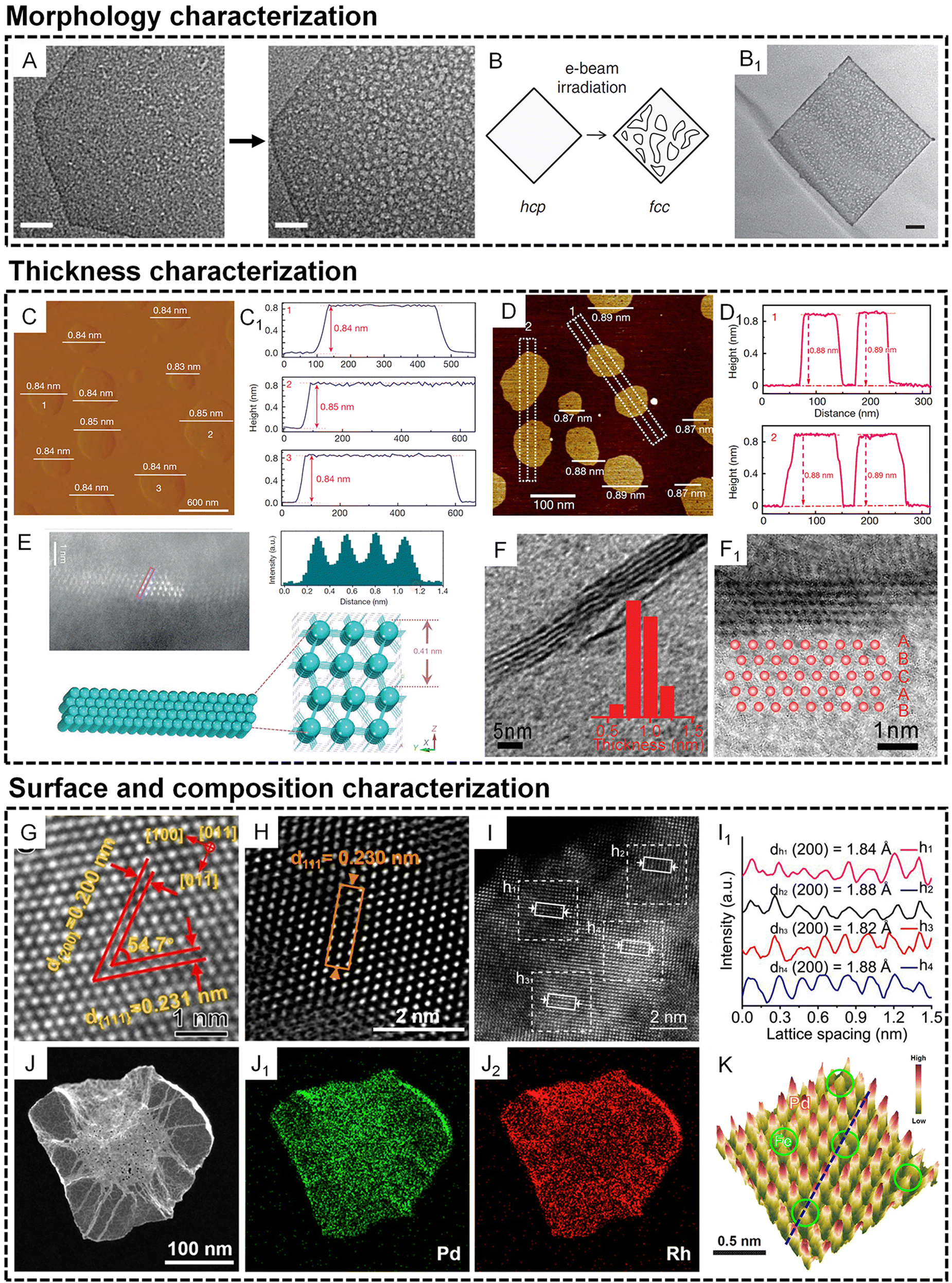 | ||
| Fig. 3 Characterization of metallenes at the nanoscale. (A and B) Morphology characterization. (A) TEM images of an individual Rh metallene after electron beam exposure for 28 s (scale bar, 20 nm). Reproduced from ref. 15 with permission from Springer Nature. Copyright 2014. (B) Scheme showing the electron beam-induced phase transformation of an Au metallene. (B1) TEM image of a porous Au metallene after electron beam irradiation for about 20 s (scale bar, 50 nm). Reproduced from ref. 31 with permission from Springer Nature. Copyright 2011. (C–F1) Thickness characterization. (C) AFM image and (C1) corresponding height profiles of Co metallene. Reproduced from ref. 22 with permission from Springer Nature. Copyright 2016. (D) AFM image and (D1) corresponding height profiles of PdMo bimetallene. Reproduced from ref. 17 with permission from Springer Nature. Copyright 2019. (E) lateral HAADF-STEM image of Co metallene and the corresponding intensity profile along the rectangle box, together with the corresponding crystal structures. Reproduced from ref. 22 with permission from Springer Nature. Copyright 2016. (F) Lateral TEM image of Rh metallene (inset shows the thickness distribution of the Rh nanosheets). (F1) HRTEM image of the cross-section of a single Rh metallene showing an ABCAB stacking sequence along the [111] axis. Reproduced from ref. 16 with permission from Wiley-VCH. Copyright 2015. (G–K) Surface and composition characterization. High-resolution high angle annular dark field scanning transmission electron microscope (HAADF-STEM) image of the surface atomic arrangement of (G) PdMo-C bimetallene, (H) RhPd-H bimetallene, and (I) high-entropy metallene. (I1) Intensity profile of the HEA phase taken from the white solid rectangles in (I). (G) Reproduced from ref. 53 with permission from American Chemical Society. Copyright 2022. (H) Reproduced from ref. 26 with permission from American Chemical Society. Copyright 2020. (I and I1) Reproduced from ref. 32 with permission from American Chemical Society. Copyright 2022. (J–J2) energy dispersive X-ray spectroscope (EDS) elemental mapping of RhPd-H bimetallene. Reproduced from ref. 26 with permission from American Chemical Society. Copyright 2020. (K) 3D topographic atom images of PdFe1 single-atom alloy metallene. Reproduced from ref. 25 with permission from Wiley-VCH. Copyright 2022. | ||
The subnanometer thickness of metallenes call for techniques with high sensitivity to the surface properties of materials. By flatly depositing metallenes on a substrate, their thickness can be directly reflected by the change of the height of the substrate surface, which can be detected by scanning probe microscopy such as atomic force microscopy (AFM). As shown in Fig. 3C and D1, partially oxidized Co metallene and PdMo metallenes with four atomic layers and a thickness below 9 angstroms can be clearly revealed by AFM.17,22 Moreover, the thickness of metallene can also be directly illustrated by their lateral view using atomic resolution scanning transmission electron microscopy (STEM)/TEM. Compared with AFM, the use of high resolution STEM/TEM not only confirms the thickness of metallenes but also clearly indicates the number of atomic layers and the corresponding atomic arrangement perpendicular to the basal planes of metallenes. As shown in Fig. 3E and F1, the lateral STEM and TEM images of Co and Rh metallenes provide evidence for the construction of the corresponding models showing the crystal structures and atomic arrangements in the metallenes.16,22
Besides morphology and thickness, other significant characteristics of metallenes are their surface properties and composition, which essentially determine their physicochemical properties. In general, the surface properties of metallenes relate to the coordination number of surface atoms which is highly dependent on surface atomic arrangement. Similar to the lateral view of metallene by atomic resolution STEM, the projection of metallene perpendicular to the basal plane can clearly indicate the atomic arrangement over the surface, which can be used for the analysis of lattice spacings along different crystallographic orientations. As demonstrated in Fig. 3G and H, the hexagonal arrangement of surface atoms was clearly observed for PdMo-C and RhPd-H metallenes. In metallenes composed of alloys, the divergence of mass contrast of surface atoms caused by different atomic numbers of involved metals can also be reflected in the STEM image, which can be analyzed by the corresponding integrated intensity profile. As shown in Fig. 3I and I1, the STEM image of pentamery metallene demonstrate square arrangement of surface atoms with distinguishable integrated pixel intensities over different regions.32 To quantitatively confirm the composition of metallene especially those consisting of solid solution alloys, typical metallic detection techniques are required, such as inductively coupled plasma mass spectrometry (ICP-MS) and inductively coupled plasma atomic emission spectrometry (ICP-AES). The distribution of different metals over the metallene can be revealed by energy dispersive X-ray spectroscopy (EDS). For example, Fig. 3J and J2 show the EDS elemental mapping of an individual metallene, clearly demonstrating the uniform distribution of Rh and Pd over the entire RhPd-H metallene. When a monometallene is doped with a trace amount of a secondary metal atoms, single atom alloy metallene can be acquired with an atomically distributed secondary metal on the surface. In this case, the detection of a single atom metal becomes much trickier, and requires characterization approaches that are usually used in the analysis of single atom alloys, such as topographic atom imaging analysis, X-ray absorption near-edge structure (XANES), and extended X-ray absorption fine structure (EXAFS). As a typical example, the presence of single Fe atoms on the surface of PdFe1 single atom alloy metallene was evidently illustrated by a well-performed 3D topographic atom imaging analysis (Fig. 3K).25 Taken together, the characterization of metallene is considerably complicated, and requires more attention relative to other metal-based nanomaterials.
3. Design of metallenes for electrocatalysis
The diversity of synthetic approaches provides the possibility to enable modification of the physicochemical properties of metallenes for electrocatalytic applications. According to the Sabatier principle, the activity of a heterogeneous catalyst is highly dependent on the interaction between its surface atoms and the intermediate(s) involved in the rate-determining step of the catalytic reaction.54 Fundamentally, the above interaction originates from the formation and occupancy of bonding and antibonding orbitals between the intermediate(s) and the catalytic site. According to this principle, the adsorption strength of intermediate species should be at a mediate value, neither too weak nor too strong, for the catalyst with an optimal activity. On the basis of the d-band theory, the change of electronic (d-band) structure can intrinsically alter the coupling strength between the adsorbate and the d-band of transition metals and thus result in the variation of their electrocatalytic activity.55 The electronic structure of metals is essentially determined by surface atomic arrangement, elemental composition, and lattice strain. In addition, the coordination number (CN) of active sites can also intrinsically alter the adsorption and dissociation energy of reactant species on a metal surface, varying the catalytic performance of electrocatalysts made of metals.56 In light of the above understanding, two major routes are adopted for the controlled synthesis of metallenes with respect to the design principles of catalyst engineering. One is modulation of electronic structure, including tuning the surface facet (facet effect), surface composition (ligand effect), and surface strain (strain effect). The other route is engineering the coordination environment of surface atoms. These general strategies are demonstrated in Fig. 4 and will be discussed in the following section.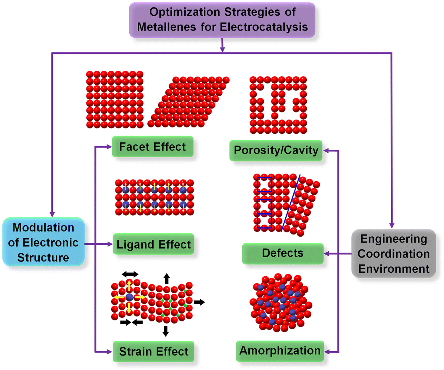 | ||
| Fig. 4 Schematic illustration of the design principle for optimizing electrocatalytic properties of metallenes. The optimization strategies are categorized into two major routes: (1) modulation of electronic structure via different routes including facet effect, ligand effect, and strain effect. (2) Engineering the coordination environment via inducing surface porosity/cavity, defects, or amorphization. | ||
3.1. Surface facet control
Since the electronic structure of transition metals is essentially determined by the atomic arrangement, designing their metallenes with well-controlled surface facets is an effective strategy to improve their electrocatalytic activity.55,57Fig. 5A clearly illustrates the three types of low-index facets, (111), (100), and (110), which are typically taken by the transition metal with an fcc structure. The difference in atomic arrangement not only changes the packing density of atoms but also varies the number of broken bonds per surface atoms, therefore leading to different specific surface free energy as well as catalytic activity of these facets.58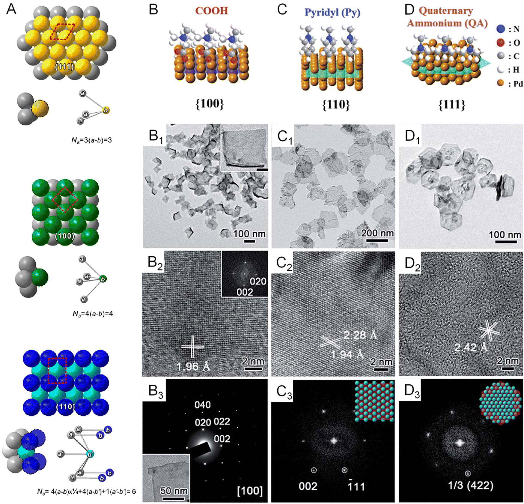 | ||
| Fig. 5 Variations in surface facets. (A) Atomic models of three major low-index planes in a metal with a fcc structure and the corresponding numbers of bonds per surface unit cell (NB) that have to be broken in creating a pair of new surfaces. The red dashed box represents the surface unit cell for each crystallographic plane. (B–D) Atomic models showing the surface binding behavior of COOH, pyridyl, and quaternary ammonium on the {100}, {110}, and {111} facets of Pd, respectively. (B1–D1) TEM images of Pd metallenes with {100}, {110}, and {111} facets exposed on the surface. (B2–D2) High resolution TEM images of Pd metallenes with {100}, {110}, and {111} facets exposed on the surface. (B3) Selected-area electron diffraction (SAED) of Pd metallenes with the {100} facet exposed on the surface. (C3 and D3) Fast Fourier transform (FFT) patterns of Pd metallenes with {110} and {111} facets exposed on the surface. (A) Reproduced from ref. 58 with permission from American Chemical Society. Copyright 2015. (B–D) Reproduced from ref. 60 with permission from the Royal Society of Chemistry. Copyright 2018. | ||
Generally, the exposed facets of metal nanocrystals synthesized by wet chemical methods can be controlled by using a well-selected capping agent which can be preferentially adsorbed on the desired planes to reduce their surface free energy and thus passivate their growth rate for exposure.59 In terms of metallenes, similar strategies can be adopted to control their surface atomic arrangement via ligand-assisted methods. For example, Liu and coworkers discovered that the selective adsorption of functional groups of COOH, pyridyl, and quaternary ammonium on different planes of Pd could induce the anisotropic growth of ultrathin Pd enclosed by {100}, {110}, and {111} facets, respectively (Fig. 5B–D).60 The length of the alkyl chain of the ligand needs to be controlled long enough to form stable lamellar mesophases for the confined growth of Pd. This tunability of surface atomic arrangement provides an opportunity to evaluate facet-dependent catalytic properties of Pd for various energy-related reactions.
3.2. Surface and subsurface composition control
Since the d-band structures varies over different transition metals, they intrinsically feature different activities on a specific catalytic reaction. For example, platinum group metals (PGMs) have been discovered as the prime catalysts for formic acid decomposition due to mediate values of heat for the formation of metal formate (ΔHf) on their surfaces and thus an optimal net reaction rate balanced by the rate of adsorption and desorption.61 Therefore, the synthesis of metallenes made of various single metals is important to study the 2D morphological effects of metals on electrocatalysis. Thanks to the synthetic capabilities developed over recent decades, a number of monometallenes, including Co, Rh, Pd, Ir, and Au, have been synthesized with well-controlled size, thickness, and surface facets (Fig. 6A–A5).13–15,31,36,62 The successful synthesis of monometallenes composed of diverse metals enables further development of bi-, tri-, and even high-entropy metallenes with improved electrocatalytic activity and selectivity.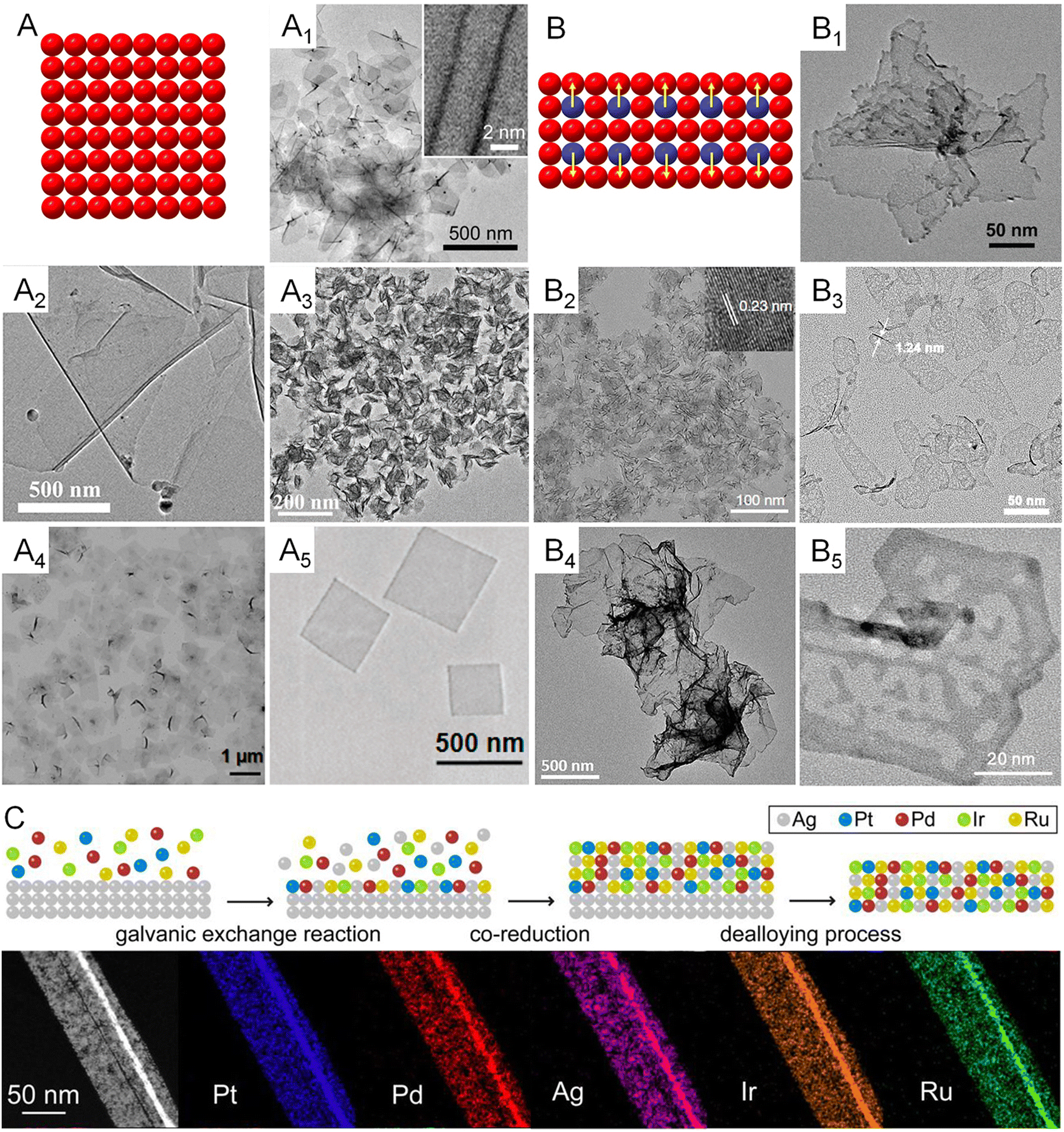 | ||
| Fig. 6 Monometallenes and metallenes composed of an alloy with expanded diversity through the incorporation of secondary metals. (A) Schematic illustration showing the atomic model of monometallenes. (A1) TEM image of Pd metallene with five-atomic-layer thickness. Reproduced from ref. 13 with permission from AAAS. Copyright 2019. (A2) TEM image of Co metallene with a thickness of 1.30 nm. Reproduced from ref. 36 with permission from American Chemical Society. Copyright 2012. (A3) TEM image of Ir metallene with a thickness of 1.05 nm. Reproduced from ref. 14 with permission from Wiley-VCH. Copyright 2022. (A4) TEM image of Rh metallene with a thickness of 0.4 nm. Reproduced from ref. 15 with permission from Springer Nature. Copyright 2014. (A5) TEM image of Au metallene with a thickness of ∼2.4 nm. Reproduced from ref. 31 with permission from Springer Nature. Copyright 2011. (B) Schematic illustration showing the atomic model of bimetallenes. (B1) TEM image of PdCu metallene with a thickness of 2.80 nm. Reproduced from ref. 65 with permission from Wiley-VCH. Copyright 2017. (B2) TEM image of PdMo metallene with a thickness of 0.88 nm. Reproduced from ref. 17 with permission from Springer Nature. Copyright 2019. (B3) TEM image of PdFe metallene with a thickness of 1.24 nm. Reproduced from ref. 64 with permission from American Chemical Society. Copyright 2022. (B4) TEM image of PdPt metallene with a thickness of 2.0 nm. Reproduced from ref. 66 with permission from the Royal Society of Chemistry. Copyright 2019. (B5) TEM image of PtPdNi trimetallene with a thickness of 1.4 nm. Reproduced from ref. 27 with permission from Wiley-VCH. Copyright 2019. (C) Schematic illustration showing galvanic exchange, co-reduction, and dealloying pathways in the synthesis of high-entropy metallene and HAADF-STEM images and EDS elemental mapping of one segment of a high-entropy PtPdIrRuAg metallene. Reproduced from ref. 32 with permission from American Chemical Society. Copyright 2022. | ||
As demonstrated in Fig. 2, the inclusion of a secondary metal element into the lattice of a transition metal can change the surrounding atoms of the surface catalytic sites and thus modify the electronic structure of the electrocatalyst, also known as the ligand effect.63 In terms of metallenes, atomic doping of the secondary metal can be controlled at either the top surface or subsurface, and both can intrinsically change the catalytic activity and selectivity of metallenes due to electron transfers between the primary and secondary metal elements. It is worth noting that the metallene structure features maximized surface area with a high surface free energy which is unfavorable for the stabilization of dopant. Therefore, sublayer doping of the secondary metals are usually adopted in the synthesis of bimetallenes, which prevents the leaching of dopant during electrocatalysis.17,64 Based on the requirements of compositions of alloys for various electrocatalytic reactions, a variety of bimetallenes and trimetallenes, including PdCu, PdMo, PdFe, PdPt, and PtPdNi, have been reported with remarkable catalytic properties (Fig. 6B–B5).17,27,64–66
When the number of metal elements increases above five in an alloy with an equant stoichiometry, the mix configuration entropy (S) of the system will pass a critical value (1.5R) which defines the concept of high-entropy alloys (HEAs). After the successful carbothermal shock synthesis of HEA nanoparticles and utilization in catalysis by the Hu group, increasing studies were conducted for the synthesis of HEA at the nanoscale with different structures for electrocatalysis.67–69 However, achieving 2D anisotropic growth of HEA remains a grand challenge owing to the distinct nucleation and growth kinetics of the composed metals and the intrinsic thermodynamic instability of 2D HEA. Very recently, Guo and coworkers proposed a general wet chemical method for generating up to an octonary HEA phase with a subnanometer ribbon structure using Ag nanowire as a template.32 As demonstrated in Fig. 6C, the production of this HEA 2D structure includes three major steps: (1) heterogeneous nucleation induced by the galvanic replacement reaction between metal ions and Ag template, (2) co-reduction of various metal ions on the Ag template, (3) removal of the Ag template by dealloying. The well-designed seed-mediated growth provided the possibility of incorporating diverse transition metals with catalytic properties into the 2D structure for the study of the effect of high-entropy alloys on electrocatalysis.
3.3. Surface strain control
Regarding the strain effect, the lattice distortion plays an essential role in shifting the d-band center of transition metals, changing the binding energy of an adsorbate on the surface of the electrocatalyst. Specifically, an expanded lattice reduces the overlap of d electrons between adjacent metal atoms, resulting in a narrowed bandwidth and the upshift of d states toward the Fermi level (EF) for the retention of d-band occupancy.70 According to the d-band center model, the upshifted d-band also lifts the antibonding state between the adsorbate and the d-band, decreasing the occupancy of the antibonding state and thus increasing the binding energy of the adsorbate.55 This fundamental correlation between surface strain and binding strength means that strain engineering is commonly used in designing electrocatalysts. In general, the lattice distortion of transition metals can be induced through four major routes: (1) epitaxial growth on a substrate with different lattice constants, (2) defect-induced lattice distortion such as vacancy, dislocation, and grain boundary, (3) the incorporation of secondary metal atoms with a different atomic radius in the lattice points, and (4) the intercalation of nonmetal atoms with small atomic radii at the interstitial sites of the lattice. With regard to metallenes, all of the routes have been reported for strain engineering. Specifically, the first route regards core-shell metal crystals with 2D morphology and a thickness of a few nanometers.9,71 The second route regards porous metallenes with a modified coordination environment of surface atoms which will be discussed in detail in Section 2.4. As discussed in Section 2.2, the third route results in bimetallenes and trimetallenes, in which the strain effect is coupled with the ligand effect for the engineering of electrocatalysts. Very recently, our group used the fourth route to synthesize Pd metallenes with controlled lattice strain.72 As demonstrated in Fig. 7A1–A4, the lattice expansion achieved by intercalations can be clearly demonstrated by an atomic resolution scanning transmission electron microscope image and X-ray diffraction pattern. A variety of nonmetal atoms, including H, C, and N, were inserted into the Pd lattice as the interstitial atoms, which offered a capability to study the difference of strain and ligand effect induced by various nonmetal elements.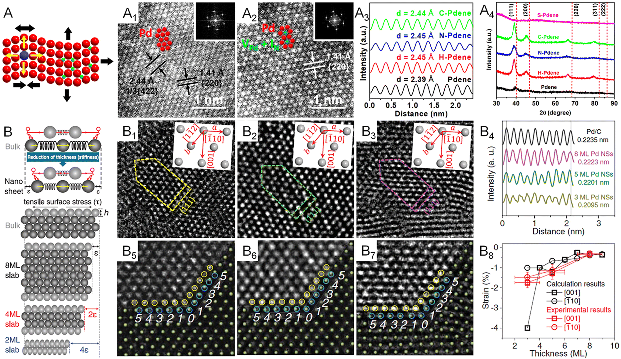 | ||
| Fig. 7 Lattice engineering of metallenes. (A) Schematic illustration showing the atomic model of metallene with lattice strain originating from curvature, doping or intercalation. (A1 and A2) Atomic-resolution HAADF-STEM images (the inset of the corresponding FFT patterns) of Pd metallene intercalated with N atoms. (A3) Integrated pixel intensity profiles and (A4) XRD patterns of Pd metallenes intercalated with H, N, and C atoms. (B) Mechanism for the generation of intrinsic strain in 2D transition metallenes. (B1–B3) high-resolution TEM images of Pd metallenes with an average thickness of (B1) three, (B2) five, and (B3) eight atomic layers on a carbon support. (B4) Intensity profiles of Pd metallenes with different thickness and Pd nanoparticles. (B5–B7) Illustration of the template-matching method used in the measurement of the lattice strain of Pd metallenes. (B8) The experimentally measured and theoretically calculated strain of Pd metallenes. (A1–A4) Reproduced from ref. 72 with permission from American Chemical Society. Copyright 2022. (B–B8) Reproduced from ref. 13 with permission from AAAS. Copyright 2019. | ||
The special 2D morphology of metallenes enables more approaches to strain engineering. The simplest way is downscaling the thickness, leading to the loss of nearby atoms and thus the reduced surface electron density. As a result, the attractive forces dominate on the surface and reduce the interatomic distance to equilibrate charge distributions. In contrast to bulk counterparts, the compressive strain caused by the contraction of surface atoms exhibit manifest effects on metallenes with a maximized ratio of surface atoms. A systematic study by the Greeley group offers a quantitative correlation between the lattice strain and the thickness of Pd metallenes.13 In this study, Pd metallenes of varying thickness were created by simply altering the CO source and the temperature environment involved in the synthesis. As shown in Fig. 7B1–B8, Pd metallenes with a compressive strain of 0.3, 1.2, and 1.5% were achieved on 8, 5, and 3 layers of Pd, respectively, demonstrating an inversely proportional correlation between intrinsic strain and thickness of Pd metallenes. In addition to the changed thickness, the curvature of metallenes caused by the minimization of surface free energy can also induce lattice distortion, leading to tensile strains generated on the surface of metallenes.17 The intrinsic tensile strains featured by highly curved metallenes have been proved to be favorable in electrocatalysis for specific reactions, which will be discussed in Section 3.1.17
3.4. Engineering of coordination environment
In addition to modulating the electronic structure of metallenes, another considerable way to regulate the adsorption behavior of adsorbates is adjusting the coordination environment of active sites. The essential descriptor of the coordination environment is CN which refers to the number of bonds formed between the atoms of interest and the neighboring atoms. For perfect crystalline materials, the CN of a surface atom is primarily determined by the lattice structure and the type of surface facet. Regarding metallenes with specific types of surface facet, inducing porosity on the surface is a specific way to modify the CN of active sites. Specifically, atoms situated at the edge of pores compose under coordinated surface sites with lower CN, greatly contributing to the catalytic activity of reactions that demand strong reaction species to active site bindings relative to saturated atoms located on the middle of the surface facet. In this regard, a variety of metallenes with a highly porous structure were reported for electrocatalysis (Fig. 8A–A3).12,14,64 Additionally, the presence of defects in imperfect crystals can also change the CN of atoms located around the defects (Fig. 8B). Therefore, altering the defect density on the surface of metallenes has also been utilized to improve the catalytic performance. As reported by Wang and coworkers, Pd metallenes with abundant Pd vacancies on the surface could provide active sites for reactant adsorption and accelerate charge transfer for the catalytic reaction (Fig. 8B1–B3).12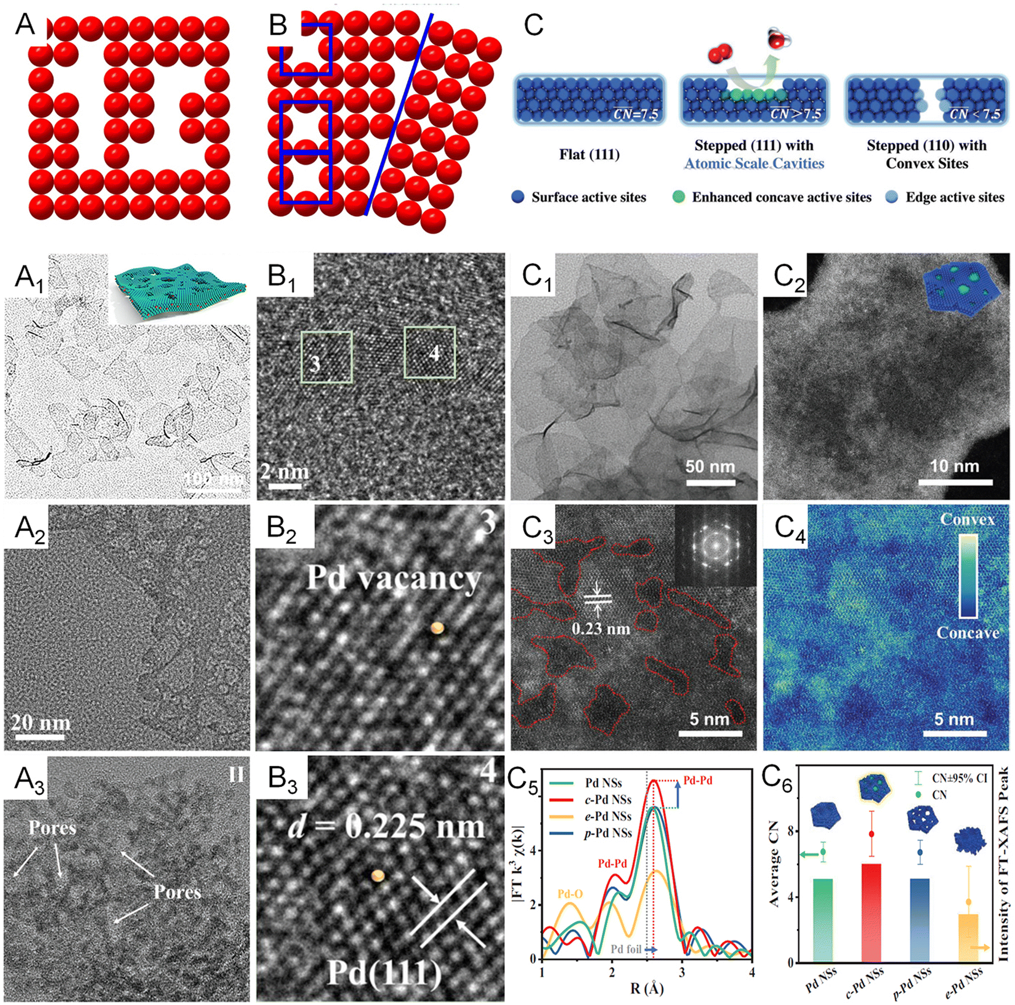 | ||
| Fig. 8 Coordination environment modulation of metallenes. (A) Schematic illustration showing the atomic model of metallene with surface porosity. (A1) TEM image of PdFe metallene with a porous and curved surface. (A2) TEM image of Pd metallene with a porous surface. (A3) TEM image of Ir metallene with a highly porous surface. (B) Schematic illustration showing the atomic model of metallene with defects. (B1–B3) High-resolution TEM image of Pd metallene with Pd vacancies on the surface. (C) Schematic illustration of the local coordination environment around flat sites, concave sites within (111) facets, and convex sites on the edges. (C1) TEM image and (C2–C4) HAADF-STEM images of Pd metallene with atomic scale cavities on the surface. (C5) Extended X-ray absorption fine structure (EXAFS) analysis of the Pd K edge of Pd metallenes with different average CN. (C6) Average CN and intensity of the FT-XAFS peak. (A1, B1–B3) Reproduced from ref. 64 with permission from American Chemical Society. Copyright 2022. (A2) Reproduced from ref. 12 with permission from Wiley-VCH. Copyright 2021. (A3) Reproduced from ref. 14 with permission from Wiley-VCH. Copyright 2022. (C–C6) Reproduced from ref. 74 with permission from Wiley-VCH. Copyright 2022. | ||
Apart from the first-nearest neighbor atoms, the coordination environment can also be affected by the extended scale of atoms. As a remarkable example, the Bandarenka group proposed the concept of “generalized” CN, which involved the effect from the adjacent atoms of first-nearest neighbor atoms on CN of active sites, to predict the electrocatalytic activity of Pt-based catalysts.73 The study concluded that Pt atoms on a concaved (111) surface with CN larger than 7.5 featured an optimal binding strength towards the adsorbates, delivering a greater catalytic performance relative to Pt atoms on a pristine (111) surface with CN of 7.5. On the basis of this generalized coordination number theory, Guo and coworkers reported local coordination regulated Pd metallenes with atomic scale surface cavities and systematically demonstrated the relationship between the CN and catalytic activity of metallenes, which will be discussed in detail in Section 3.1.74 Another important way to change the coordination environment of active sites is amorphization of metallenes by ligand exchange or intercalation of nonmetal atoms.72,75 As shown in Fig. 9A–A1, partially amorphous Pd metallene intercalated with S atoms can be obtained from crystalline Pd metallene via solvothermal sulphuration.72 Besides, Zhang and coworkers reported ligand-exchange-induced amorphization of Pd, in which an order to disorder phase transition of fcc Pd was achieved by a thiol molecule (1,3,4-thiadiazole-2,5-dithiol, C2H2N2S3), namely bismuthiol I, under ambient conditions without destroying their original morphologies (Fig. 9B–B5).75 The reduced crystallinity caused by amorphization not only increases the distance between metal atoms but also changes the coordination numbers of active sites on the surface, resulting in a large alteration of the electronic structure of metallenes for improved electrocatalytic performance.72,75
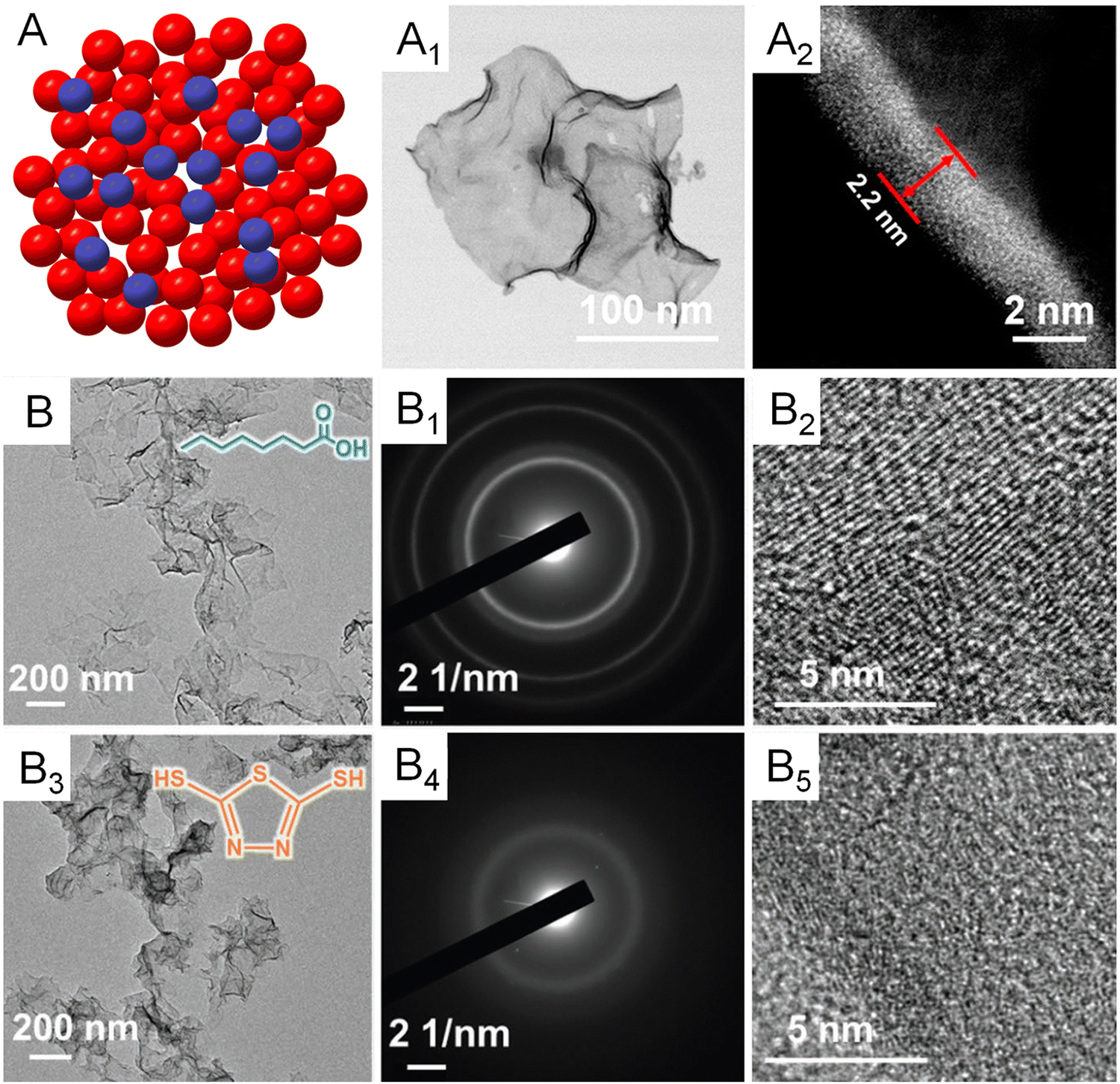 | ||
| Fig. 9 Amorphization of metallenes. (A) Schematic illustration showing the atomic model of amorphous metallene with a disordered surface atomic arrangement. (A1) TEM image and (A2) the lateral HAADF-STEM image of amorphous Pd metallene doped with S atoms. Reproduced from ref. 72 with permission from American Chemical Society. Copyright 2022. (B) TEM image, (B1) SAED pattern, and (B2) HRTEM image of crystalline Pd metallene (the inset shows the molecular structure of octanoic acid). (B3) TEM image, (B4) SAED pattern, and (B5) HRTEM image of amorphous Pd metallene. (The inset shows the molecular structure of bismuthiol I). Reproduced from ref. 75 with permission from Wiley-VCH. Copyright 2020. | ||
4. Electrocatalysis and photocatalytic energy conversion
Given the intriguing structural and electronic properties and the aforementioned design strategies, 2D metallenes, especially those made of noble metals, have attracted increasing attention in a wide range of electrocatalysis and devices for energy conversion, including water splitting, CO2 reduction, fuel cells, and metal-air batteries.11,19 Here we summarize the recent progress in utilizing metallenes as electrocatalysts for diverse catalytic reactions, including the oxygen reduction reaction (ORR), hydrogen evolution reaction (HER), alcohol and acid oxidation, CO2 reduction (CO2RR), and nitrogen reduction reaction (NRR), as well as photocatalysts for energy conversion.4.1. Oxygen reduction reaction
As the cathodic reaction in fuel cells, the ORR has sluggish kinetics and limits the commercialization of the device.76–78 Although state-of-the-art Pt-based catalysts can essentially accelerate the ORR kinetics, the high price of Pt greatly increases the cost of fuel cells and hinders the extensive application of this class of catalyst.79–81 Therefore, exploring catalysts with considerable activity relative to that of Pt is a considerable strategy for the commercialization of fuel cells. Recently, 2D Pd-based catalysts were identified as an alternative to Pt. With a structure of maximized AUE, Pd metallenes with atomic thickness feature abundant active sites on the surface for a superior ORR mass activity. As discussed in Section 2, the ORR activity of Pd metallenes can be further improved by dopants, thickness control, and modification of the coordination environment of surface atoms. For example, the PdMo metallenes reported by the Guo group delivered a mass activity of 16.37 A mgPd−1 at 0.9 V versus the reversible hydrogen electrode (RHE) in alkaline electrolytes, which was 78 and 327 times higher than those of commercial Pt/C and Pd/C catalysts, respectively.17 The enhanced ORR performance could be attributed to the significant ligand effect induced by the doping of Mo atoms into Pd metallene with intrinsic surface tensile strains, in which charge transfer downshifted the d-band center by 0.26 eV relative to the pure Pd metallene and moved the binding energy of oxygen (ΔEO) toward the optimal value for the ORR (Fig. 10A–A3).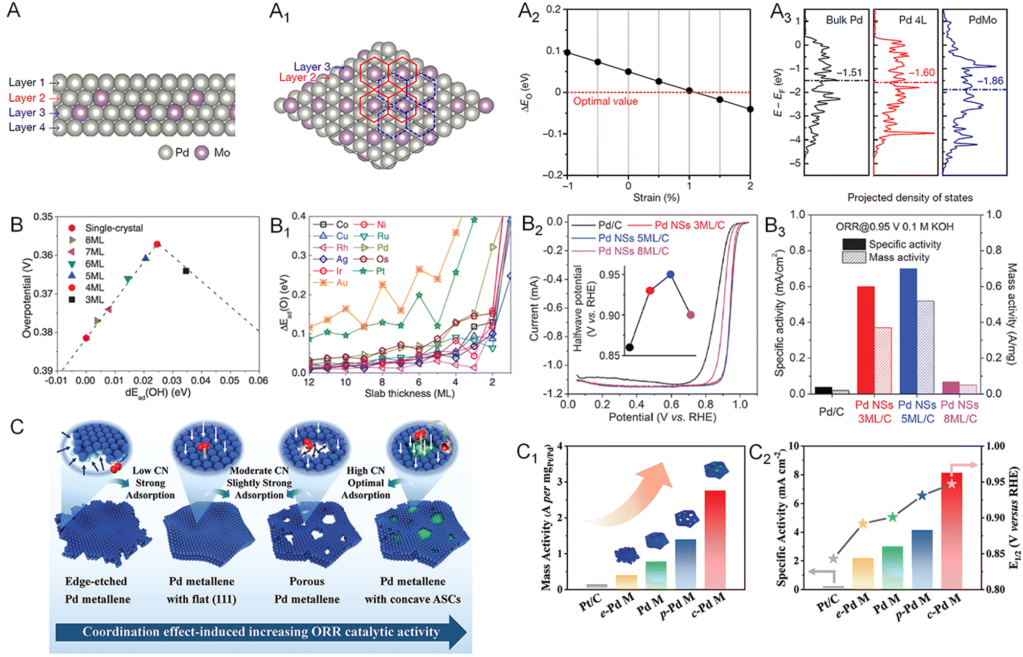 | ||
| Fig. 10 Utilization of metallenes in the ORR. (A) Side and (A1) top view of the atomic model of the four-layer PdMo bimetallene. (A2) ΔEO of PdMo bimetallene as a function of compressive (negative) and tensile (positive) strains. (A3) The projected electronic density of states of the d-band for the surface palladium atoms in bulk Pd, a four-layer Pd metallene (Pd 4L) and PdMo bimetallene. (B) Adsorption energy shift of atomic oxygen on strained fcc (111) and hcp (0001) slabs, compared with adsorption energies on the corresponding close-packed single-crystal surfaces. (B1) The predicted ORR overpotential of Pd(110) single-crystal and strained metallenes with various thicknesses. (B2) ORR polarization curves of Pd metallenes with different average thickness in 0.1 M KOH (the inset shows the halfwave potential). (B3) Specific activity and mass activity of the ORR at 0.95 V versus RHE in 0.1 M KOH and the corresponding improvement factors compared to those for Pd nanoparticles. (C) Schematic illustration of the coordination effect in ORR electrocatalysis based on Pd metallene samples with different active site structures. (C1) Mass activity, (C2) specific activity at 0.9 V versus RHE and half-wave potential of Pd metallenes with different average CN. (A1–A3) Reproduced from ref. 17 with permission from Springer Nature. Copyright 2019. (B–B3) Reproduced from ref. 13 with permission from AAAS. Copyright 2019. (C–C2) Reproduced from ref. 74 with permission from Wiley-VCH. Copyright 2022. | ||
The ORR performance of Pd metallene can also be finely tuned by altering their thickness. As demonstrated by the Wang group, the Pd metallene with a thickness of five monolayers delivered a higher ORR activity relative to those with three and eight monolayers in both acidic and alkaline electrolytes (Fig. 10B–B3).13 The optimal performance of five monolayer metallene arises from the optimal compressive surface strain, generating appropriate binding between the oxygen species and the surface atoms. Regarding the engineering of coordination environment, Guo and coworkers reported Pd metallenes with a series of average CN of surface atoms to systematically study the CN-dependent ORR activity of Pd.74 As shown in Fig. 10C–C3, the Pd metallene with an average CN of about 7.83 exhibited the highest activity and half-wave potential owing to the elevated CN and moderately downshifted d-band center.
4.2. Hydrogen evolution reaction
As a key half reaction for hydrogen production via water splitting, the HER is usually catalyzed by noble metals such as Pt, Pd, Ir, and Rh. Taking advantage of the 2D morphology, a variety of noble metallenes have been utilized in the HER with outstanding performance. For instance, Cheng and coworkers demonstrated that defective and porous Ir metallenes delivered a superior HER performance with an overpotential of 14 mV at a current density of 10 mA cm−2, a Tafel slope of 31.2 mV dec−1, and a double-layer capacitance of 4.30 mF cm−2.14 The HER activity of Ir metallene surpassed that of Pt/C due to the large specific surface area, high conductivity, and efficient mass transfer benefitting from the ultrathin 2D morphology. In addition, the partially hydroxylated surface achieved by polyallylamine (PAH) modification featured a modulated electronic structure and efficient proton carriers, which is favorable to the HER in acidic media. As discussed in Section 2.1, the exposed facet on the surface of metallenes can also alter their HER performance. The facet-dependent HER activity was investigated by Liu and coworkers, comparing the HER activity of Pd metallenes with (100), (111), and (110) facets.60 Due to the optimal balance between hydrogen adsorption and desorption on Pd(100) planes, the Pd metallene with a surface facet of (100) planes showed the lowest overpotentials at current densities of 10, 50, and 100 mA cm−2 in an acidic electrolyte relative to those exposed with (111) and (110) planes (Fig. 11A and A1). Moreover, the anisotropic 2D morphology could largely retard the electrochemical dissolution and ripening process of Pd metallene, realizing excellent HER durability with a slight degradation over 20 h (Fig. 11A2 and A3).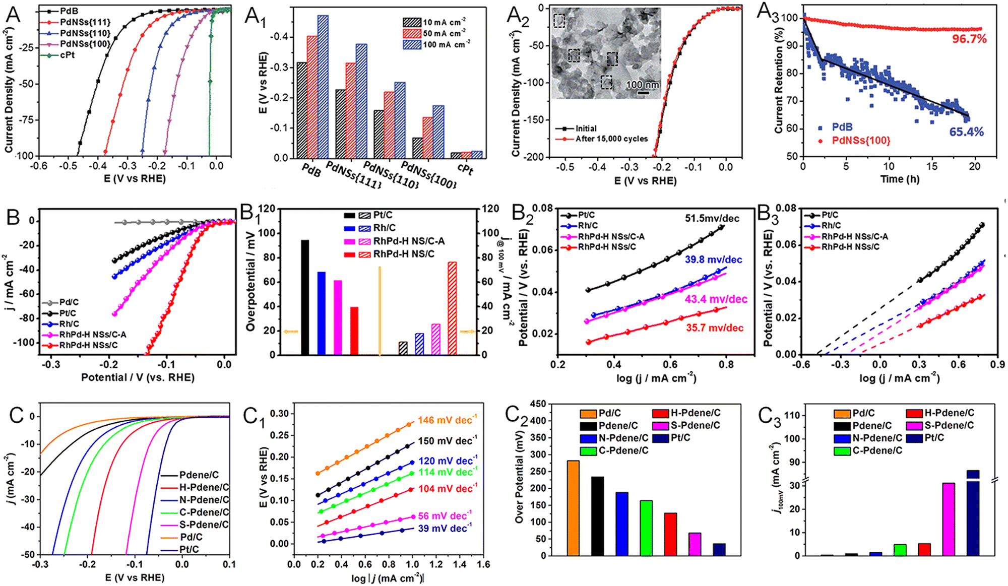 | ||
Fig. 11 Utilization of metallenes in the HER. (A) Polarization curves and (A1) overpotentials at current densities of 10, 50, and 100 mA cm−2 of Pd metallenes with different surface facets. (A2) Polarization curves of Pd metallenes with the (100) facet before and after repeating potential scans of 15![[thin space (1/6-em)]](https://www.rsc.org/images/entities/char_2009.gif) 000 cycles. (A3) Chronoamperometric curves of Pd metallenes with the (100) facet and commercial Pd black under a constant overpotential of 42 mV. (B) Polarization curves, (B1) overpotential at 10 mA cm−2 and current density at 100 mV, the corresponding (B2) Tafel plots and (B3) exchange current density of RhPd-H bimetallene compared with commercial Pt/C and Rh/C in 1.0 M H2SO4 electrolyte. (C) Polarization curves, (C1) corresponding Tafel plots, (C2) overpotentials at a current density of 10 mA cm−2, and (C3) current density at 100 mV of crystalline and amorphous Pd metallenes in 1.0 M KOH electrolyte. (A–A3) Reproduced from ref. 60 with permission from the Royal Society of Chemistry. Copyright 2018. (B–B3) Reproduced from ref. 26 with permission from American Chemical Society. Copyright 2020. (C–C3) Reproduced from ref. 72 with permission from American Chemical Society. Copyright 2022. 000 cycles. (A3) Chronoamperometric curves of Pd metallenes with the (100) facet and commercial Pd black under a constant overpotential of 42 mV. (B) Polarization curves, (B1) overpotential at 10 mA cm−2 and current density at 100 mV, the corresponding (B2) Tafel plots and (B3) exchange current density of RhPd-H bimetallene compared with commercial Pt/C and Rh/C in 1.0 M H2SO4 electrolyte. (C) Polarization curves, (C1) corresponding Tafel plots, (C2) overpotentials at a current density of 10 mA cm−2, and (C3) current density at 100 mV of crystalline and amorphous Pd metallenes in 1.0 M KOH electrolyte. (A–A3) Reproduced from ref. 60 with permission from the Royal Society of Chemistry. Copyright 2018. (B–B3) Reproduced from ref. 26 with permission from American Chemical Society. Copyright 2020. (C–C3) Reproduced from ref. 72 with permission from American Chemical Society. Copyright 2022. | ||
The HER activity of metallenes can be further improved via inducing a strain and ligand effect achieved by the incorporation of either metallic or nonmetallic elements. For example, bimetallenes such as RuRh and IrRh metallenes have been demonstrated as outstanding electrocatalysts towards the HER.82,83 In addition to forming alloys, intercalation of light atoms, defined as being within the third-row elements, has also been proved an effective way to modify the electronic structure of metallenes.84–88 Different from the secondary metal atoms located at the lattice point of metallenes, the much smaller atomic radii of light atoms enable them to permeate into the interstitial sites of the lattice, inducing lattice enlargement and charge transfer between the host and guest atoms. This strain and ligand effect caused by light atoms enhances the catalytic activity and selectivity of metallenes. As reported by the Zheng group, the RhPd bimetallene with interstitial H atoms (RhPd-H) exhibited the lowest overpotential at a current density of 10 mA cm−2, the highest current density at an overpotential of 100 mV versus RHE, and the lowest Tafel slope relative to those of Rh/C and Pt/C in alkaline media (Fig. 11B–B2).26 The enhanced HER activity could be ascribed to modulation of the surface electronic state, bond distance, and CN of Rh and Pd atoms achieved by the presence of interstitial H atoms, resulting in a desirable hydrogen adsorption energy and thus accelerating the rate of hydrogen gas production.84 The RhPd-H bimetallene also delivered an outstanding HER durability due to the ultrathin 2D sheet-like morphology with a faster electron and mass transfer rate on the open double-sided surfaces (Fig. 11B3). The amorphization of Pd metallene can also enhance the HER activity. As reported by our group, the sulphuration-induced Pd amorphization resulted in the greater HER performance of Pd–S metallene relative to those of the crystalline counterparts (Fig. 11C–C3).72 This improvement can be ascribed to the well-modified electronic structure caused by the ligand effect and amorphous structure. The elongated Pd–Pd bond length and increased d-band downshift in amorphous structure weakened the hydrogen bonding and thus improved the HER activity. The disordered surface and presence of S atoms also altered the coordination environment of surface Pd atoms, potentially providing abundant active sites on Pd–S metallene for the HER.
4.3. Alcohol and acid oxidation reaction
Chemical fuels, such as formic acid, ethanol, and ethylene glycol, are commonly used in the anodic reaction in direct liquid fuel cells.77,89 The oxidation reactions of these chemicals can be greatly promoted when using Pt- and Pd-based electrocatalysts.90–93 Owing to the largely exposed surface area, abundant active sites, and excellent poisoning resistance, Pd-based metallenes have been widely used in these oxidation reactions.65,66,94,95 Moreover, the electrocatalytic activity can be further improved when alloying Pd with other metal or nonmetal elements to modify the electronic structure and crystal phase. By alloying Pd with Cu, Zhang and coworkers reported ultrathin PdCu bimetallenes with a superior mass activity of 1.66 A mgPd−1 toward the formic acid oxidation reaction (FAOR), which was about 14 times higher than that of commercial Pd black (Fig. 12A–A3).65 The enhancement in FAOR activity could be attributed to the 2D morphology, the ligand effect between Pd and Cu, and the maximized exposure of surface active sites by the post-treatment with ethylenediamine (EN).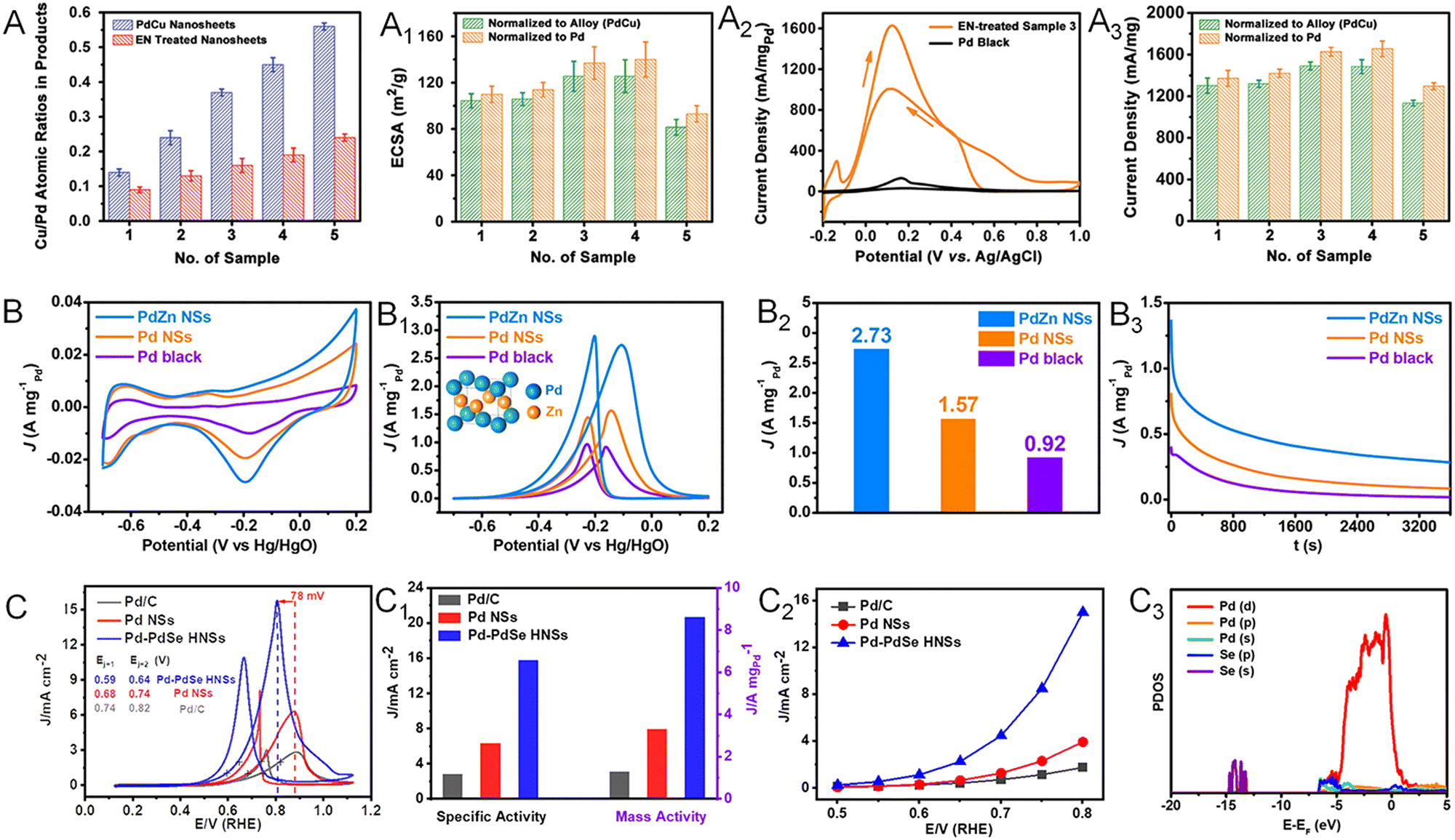 | ||
| Fig. 12 Utilization of metallenes in chemical fuel oxidation. (A) PdCu metallenes with different atomic ratios of Cu to Pd. (A1) ECSAs of PdCu metallenes recorded in 0.5 M H2SO4 aqueous solution. (A2) CV curves of EN-treated PdCu metallene with a Cu/Pd ratio of 0.45 (Sample 3) and Pd black. (A3) Peak current densities of PdCu metallenes in an electrocatalytic FAOR recorded in aqueous solution containing 0.5 M H2SO4 and 0.25 M HCOOH. (B) CV curves of PdZn bimetallene, Pd metallene, and Pd black tested in 1.0 M NaOH aqueous solution. (B1) CV curves of PdZn bimetallene, Pd metallene, and Pd black measured in a mixture of 1.0 M NaOH and 1.0 M ethanol. (B2) Mass activities of PdZn bimetallene, Pd metallene, and Pd black at their respective peak potentials in the CV profiles in (B1). (B3) EOR chronoamperometric stability profiles of PdZn bimetallene, Pd metallene, and Pd black tested at -0.2 V versus Hg/HgO. (C) Cyclic voltammogram curves, (C1) specific and mass activity, (C2) specific activity at the indicated potentials of Pd–PdSe metallene. (C3) The partial density of states (PDOS) of the Se-doped Pd(111) surface. (A–A3) Reproduced from ref. 65 with permission from Wiley-VCH. Copyright 2017. (B–B3) Reproduced from ref. 94 with permission from American Chemical Society. Copyright 2019. (C–C3) Reproduced from ref. 95 with permission from Wiley-VCH. Copyright 2020. | ||
Alloying Pd with another transition metal and basic metals such as Zn, Cd, and Pb can not only alter the electronic structure but also result in phase transition of Pd.94,96 For example, Zhang and coworkers demonstrated the successful synthesis of PdZn and PdCd bimetallenes with a face-centered tetragonal (fct) structure.94 The PdZn bimetallene displayed an improved mass activity of 2.73 A mgPd−1 toward the ethanol oxidation reaction (EOR), which was 1.74 and 2.97 fold higher than those of Pd metallene and commercial Pd black, respectively (Fig. 12B–B3). Apart from the 2D nature with plenty of undercoordinated active sites on the surface, the improved EOR performance of PdZn bimetallene might also result from the unique electronic and crystal structure caused by the incorporation of Zn into the Pd lattice, together with the polycrystalline structure of the metallene with extra active sites for the EOR. When alloying Pd with p-block nonmetal elements, the unconventional p–d hybridization interaction between the d orbital of Pd and p orbital of nonmetal elements can bring remarkable improvement of electrocatalytic properties of Pd.97 As reported by the Zhang group, Pd metallene doped with Se atoms (Pd–PdSe) could exhibit 6.6 and 2.6 fold enhancement in mass activity for the ethylene glycol oxidation reaction (EGOR) compared with those of Pd metallene and commercial Pd/C (Fig. 12C–C2).95 Both experimental results and theoretical calculations revealed the existence of strong p–d orbital hybridization and tensile train in Pd–PdSe bimetallene, which could reduce the activation energy of C–C bond cleavage and accelerate CO* oxidation and thus boost the complete oxidation of EG (Fig. 12C3).
4.4. Carbon dioxide reduction reaction
Converting CO2 into chemical fuels, such as methane, methanol, formate, ethylene, and ethanol, is one of the most considerable strategies for addressing the global energy crisis.98 To date, both noble (Pd, Ag, Au) and non-noble metals (Co, Cu, Zn, Bi) have been involved in the catalysis of the CO2RR.99 Remarkably, 2D non-noble metal-based electrocatalysts have attracted increasing research interest because of the maximized AUE and higher cost-effectiveness relative to noble metals.19 For instance, Xie and coworkers prepared partially oxidized Co metallene with four-atomic-layer thickness for highly selective electroreduction of CO2 to formate (Fig. 13A).22 As demonstrated in Fig. 13A1 and A2, a stable current density of 10.59 mA cm−2 and a high faradaic efficiency (FE) of 90.1% could be achieved at an overpotential of 0.24 V versus RHE, which were substantially remained over 40 h. The study suggests that regulation of the oxidation state of 2D metallenes plays a key role in improving the catalytic properties of the CO2RR, offering a design principle for the engineering of active sites at an atomic scale. In another example, ultrathin bismuthene with an average thickness of 1.28–1.45 nm was prepared by Xu and coworkers.43 When used as an CO2RR catalyst, a nearly 100% FE for formate and a partial current density up to 72 mA cm−2 were obtained in a wide potential window over 0.35 V (Fig. 13B). To further evaluate the feasibility of bismuthene in energy-related devices, the catalyst was also applied in a self-designed flow cell and a bipolar membrane separated fuel cell (Fig. 13B1). The bismuthene could deliver a steady current density of 100 and 200 mA cm−2 at −0.57 and −0.75 V versus RHE, respectively, with FE close to 100%, meeting the requirements for commercial application. Meanwhile, a new pathway with the direct involvement of HCO3− in the CO2RR process for formate production was proposed based on in situ attenuated total reflection-infrared (ATR-IR) spectroscopy analysis combined with theoretical calculation (Fig. 13B2 and B3).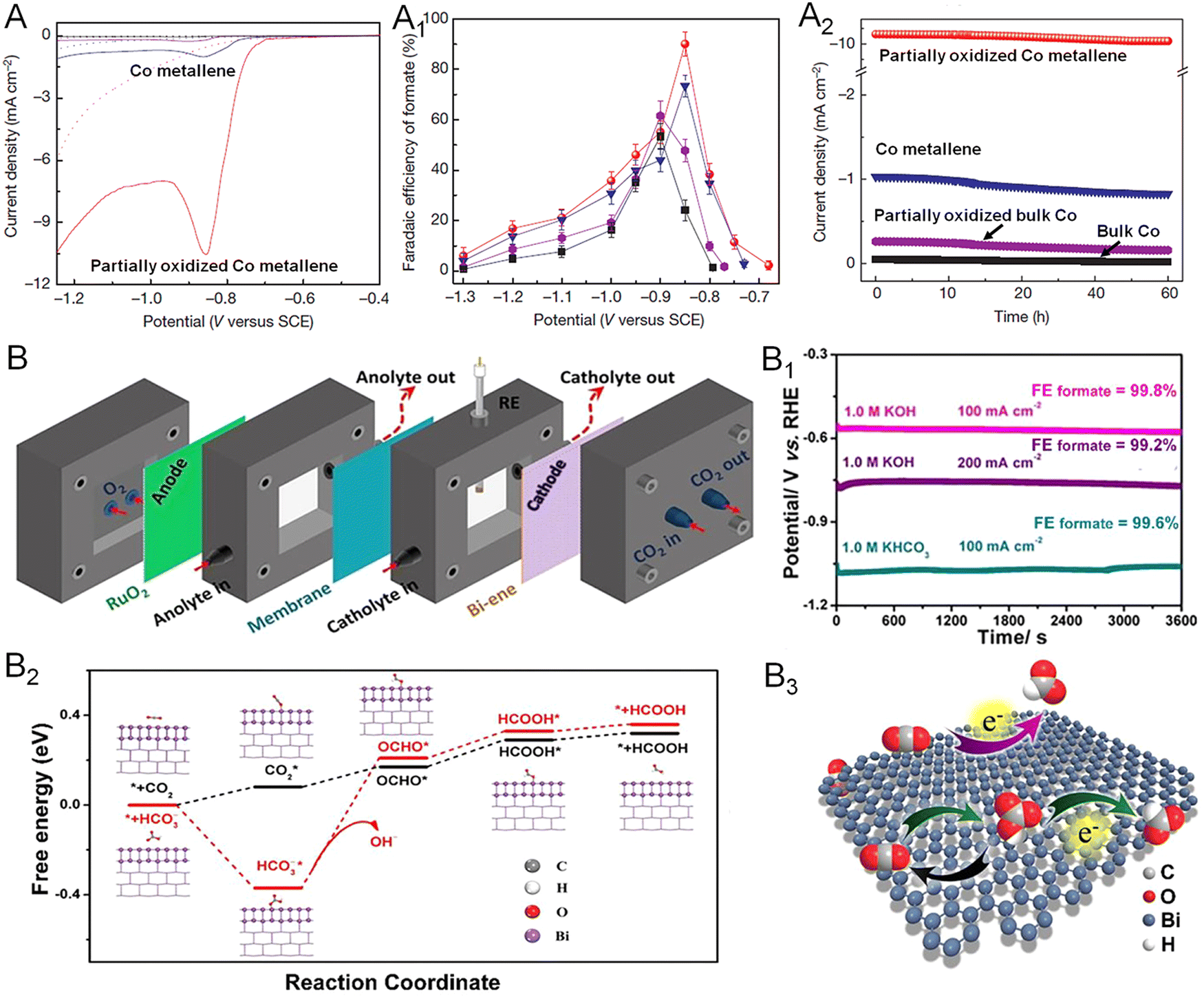 | ||
| Fig. 13 Utilization of metallenes in the CO2RR. (A) Linear sweep voltametric curves of Co metallenes in a CO2-saturated (solid line) and N2-saturated (dashed line) 0.1 M Na2SO4 aqueous solution. (A1) Faradaic efficiencies of formate at each given potential for 4 h. (A2) Chrono-amperometry results at the corresponding potentials (in A1) with the highest faradaic efficiencies. (B) Diagram of the self-designed flow cell. (B1) Chronopotentiometric curves of bismuthene at 100 and 200 mA cm−2 in 1.0 M KHCO3 and KOH. (B2) Free-energy diagrams for HCOOH over bismuthene. (B3) Proposed electrocatalytic CO2RR mechanism over bismuthene. (A–A2) Reproduced from ref. 22 with permission from Springer Nature. Copyright 2016. (B–B3) Reproduced from ref. 43 with permission from Wiley-VCH. Copyright 2020. | ||
4.5. Nitrogen reduction reaction
Production of ammonia by direct reduction of N2 under ambient conditions becomes a promising alternative way relative to the conventional Haber–Bosch process in the industrial production of fertilizer. However, the high bond energy of the N![[triple bond, length as m-dash]](https://www.rsc.org/images/entities/char_e002.gif) N triple bond and the competing HER lead to an unsatisfactory faradaic efficiency (FE) of NRR for NH3 production.100 Besides, the involved dissociative and associative mechanisms make the NRR process complicated and less understandable. Therefore, well-designed electrocatalysts are required to perform the experimental and theoretical studies and thus overcome these issues associated with the NRR. Among the catalysts reported, Pd-based nanomaterials have recently emerged as an excellent catalyst for the NRR with high activity and selectivity for NH3 production. The NRR performance can be fundamentally improved by facilitating the adsorption and activation of N2 on the surface of Pd, which can be realized by the intercalation of lattice hydrogen atoms as well as engineering lattice vacancies of Pd.101,102 As such, the synthesis of Pd-H metallene with surface vacancies serves as a promising strategy for the generation of a highly efficient NRR catalyst. As reported by Wang and coworkers, electrochemical conversion of N2 to NH3 can be performed and catalyzed by Pd-H metallene with Pd vacancies in a three-electrode H-cell under ambient conditions (Fig. 14A).103 The yield rate and FE of NH3 at different applied potentials is shown in Fig. 14A1, which can be well-maintained within 10 cycles (Fig. 14A2). The NRR mechanism on the surface of Pd-H metallene was studied by in situ Raman spectroscopy, indicating an association pathway of the NRR as demonstrated in Fig. 14A3 and A4. Doping Pd with another NRR active material such as Fe, Co, and Cu is another effective way to improve the intrinsic activity and selectivity of Pd metallene. As shown in Fig. 14B and B1, theoretical simulations were conducted to demonstrate the enhanced N2 adsorption preference to the Pd-coordinated isolated Fe atoms on the surface of PdFe1 single atom alloy metallene.25 The electron-deficient Fe atoms can act as a Lewis acid site to attract the lone pair electrons of Lewis base N2 with a hole-rich region, suggesting the activated N2 on PdFe1 metallene. As shown in Fig. 14B2, the PdFe1 metallene delivered the highest NH3 yield of 111.9 μg h−1 mg−1 and FE of 37.8% at −0.2 V, indicating the exceptional NRR activity and selectivity. The PdFe1 metallene also exhibited excellent electrochemical stability with a steady current density in the chronoamperometry test for 100 h continuous NRR electrolysis and no apparent degradation in NH3 yields and FEs during the cycling tests (Fig. 14B3).
N triple bond and the competing HER lead to an unsatisfactory faradaic efficiency (FE) of NRR for NH3 production.100 Besides, the involved dissociative and associative mechanisms make the NRR process complicated and less understandable. Therefore, well-designed electrocatalysts are required to perform the experimental and theoretical studies and thus overcome these issues associated with the NRR. Among the catalysts reported, Pd-based nanomaterials have recently emerged as an excellent catalyst for the NRR with high activity and selectivity for NH3 production. The NRR performance can be fundamentally improved by facilitating the adsorption and activation of N2 on the surface of Pd, which can be realized by the intercalation of lattice hydrogen atoms as well as engineering lattice vacancies of Pd.101,102 As such, the synthesis of Pd-H metallene with surface vacancies serves as a promising strategy for the generation of a highly efficient NRR catalyst. As reported by Wang and coworkers, electrochemical conversion of N2 to NH3 can be performed and catalyzed by Pd-H metallene with Pd vacancies in a three-electrode H-cell under ambient conditions (Fig. 14A).103 The yield rate and FE of NH3 at different applied potentials is shown in Fig. 14A1, which can be well-maintained within 10 cycles (Fig. 14A2). The NRR mechanism on the surface of Pd-H metallene was studied by in situ Raman spectroscopy, indicating an association pathway of the NRR as demonstrated in Fig. 14A3 and A4. Doping Pd with another NRR active material such as Fe, Co, and Cu is another effective way to improve the intrinsic activity and selectivity of Pd metallene. As shown in Fig. 14B and B1, theoretical simulations were conducted to demonstrate the enhanced N2 adsorption preference to the Pd-coordinated isolated Fe atoms on the surface of PdFe1 single atom alloy metallene.25 The electron-deficient Fe atoms can act as a Lewis acid site to attract the lone pair electrons of Lewis base N2 with a hole-rich region, suggesting the activated N2 on PdFe1 metallene. As shown in Fig. 14B2, the PdFe1 metallene delivered the highest NH3 yield of 111.9 μg h−1 mg−1 and FE of 37.8% at −0.2 V, indicating the exceptional NRR activity and selectivity. The PdFe1 metallene also exhibited excellent electrochemical stability with a steady current density in the chronoamperometry test for 100 h continuous NRR electrolysis and no apparent degradation in NH3 yields and FEs during the cycling tests (Fig. 14B3).
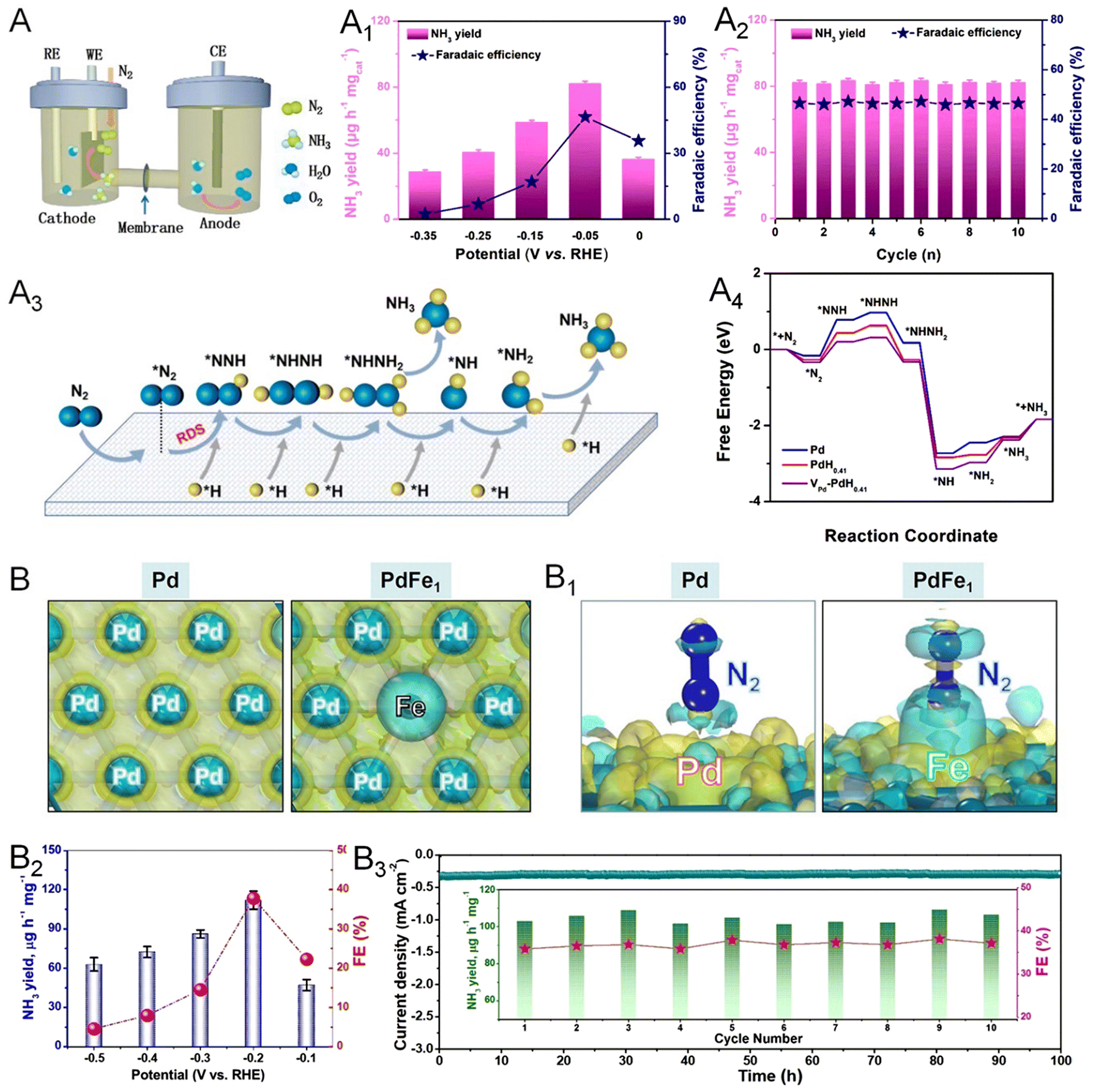 | ||
| Fig. 14 Utilization of metallenes in the NRR. (A) Diagram of the H-cell for NH3 production. (A1) NH3 yield and corresponding FEs of interstitial Pd-H metallene with vacancies at given potentials in N2-saturated electrolyte. (A2) Recycling test of the NRR for 10 times of Pd-H metallene at −0.05 V versus RHE. (A3) A simplified N2 generation mechanism on the surface of Pd-H metallene. (A4) Free-energy diagrams of the NRR on Pd nanosheets and Pd-H metallenes with and without vacancies. (B) NH3 yield and corresponding FEs of PdFe1 single-atom alloy metallene. (B1) Chronoamperometry test at −0.2 V for 100 h of PdFe1 single-atom alloy metallene (inset of the cycling test). (B2) Differential charge densities of Pd and PdFe1. Yellow: electron accumulation, cyan: electron depletion. (B3) Differential charge densities of absorbed N2 on Pd and PdFe1. (A–A4) Reproduced from ref. 102 with permission from Elsevier. Copyright 2022. (B–B3) Reproduced from ref. 25 with permission from Wiley-VCH. Copyright 2022. | ||
4.6. Photocatalysis
Beyond the electrochemical reactions mentioned above, some metallenes also performed well in photocatalytic reactions. For example, Sun and coworkers reported the defect engineering of two-dimensional oxidized Sb metallene to activate intrinsically inert Sb for efficient visible light-driven NRR to produce NH3.103 Compared with bulk Sb and Sb2O3, the Sb metallene delivered substantially enhanced N2 photofixation with remarkable NH3 yield rates, likely resulting from the plentiful surface catalytic sites associated with atomic thickness and a high density of active surface defects to greatly facilitate charge carrier migration and separation (Fig. 15A). The defective Sb metallene maintained good stability and thus reusability without apparent decays in activity after five cycling tests (Fig. 15A1). In another example of photocatalytic applications, Bi metallene served as an electron mediator in a 2D Z-scheme photocatalyst for the CO2RR.104 In the photoelectrochemical experiment, high cathode photocurrent densities were observed for the photocatalyst, indicating an enhanced charge utilization efficiency in either the oxidation or the reduction reaction (Fig. 15B and B1). Moreover, no significant photocurrent change was observed within 2000 s at a constant bias of 0.6 V versus RHE, confirming the satisfactory photoelectrochemical stability of the catalyst (Fig. 15B2).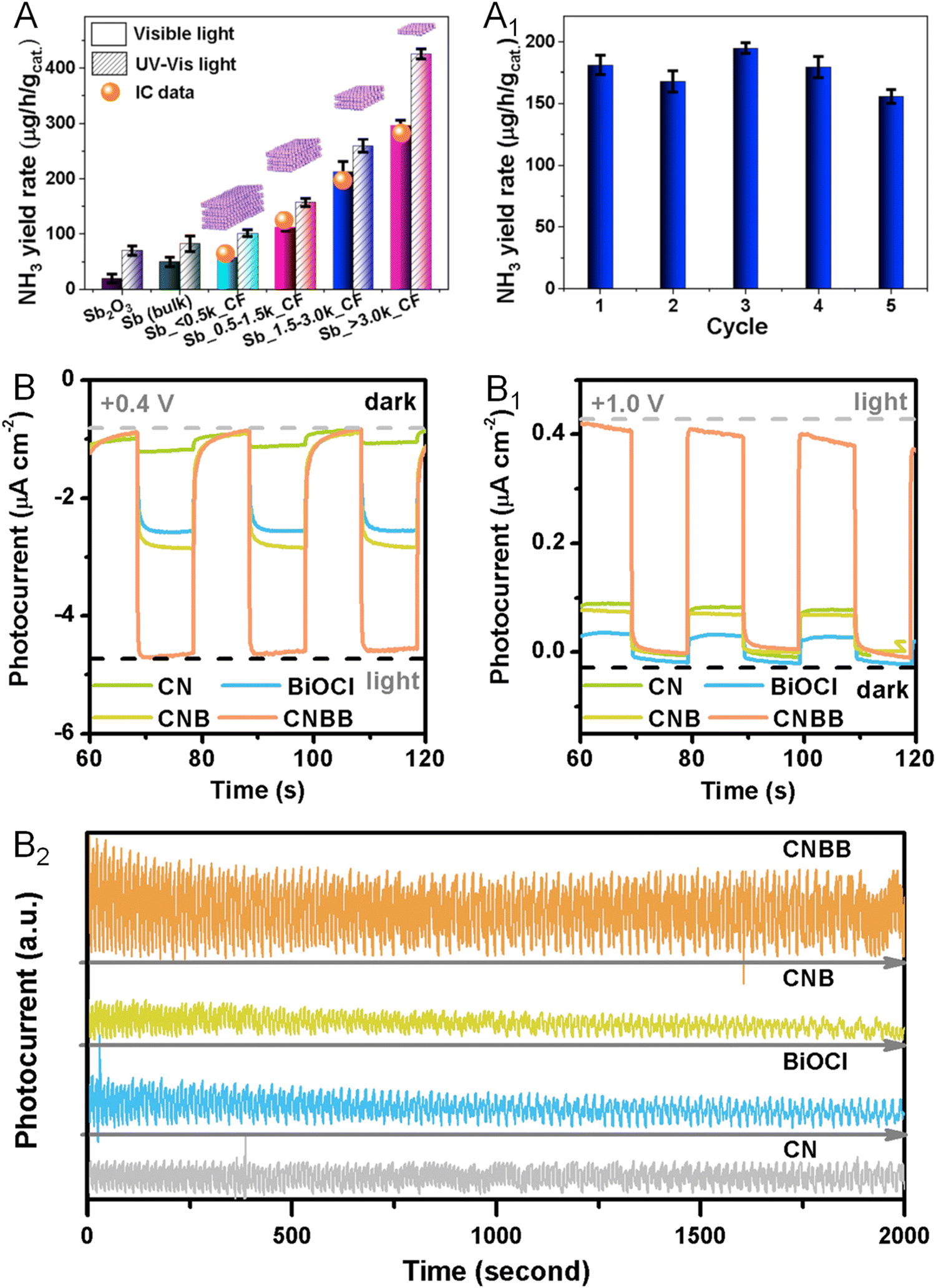 | ||
| Fig. 15 Utilization of metallenes in photocatalysis. (A) NH3 yield rates under UV-Vis or visible light irradiation over antimonene. (A1) NH3 yield rate of antimonene against recycling cycle. (B–B2) Transient photocurrent responses of bismuthene for the CO2RR at 0.4, 1.0, and 0.6 V versus RHE. (A and A1) Reproduced from ref. 103 with permission from Elsevier. Copyright 2020. (B–B2) Reproduced from ref. 104 with permission from American Chemical Society. Copyright 2021. | ||
5. Conclusions and perspectives
Taking advantage of the rapid advancement of synthetic techniques at the nanoscale, remarkable development has been made in the synthesis of metallenes. This minireview summarizes the recent progress in this domain, highlighting the synthesis, characterization, and design principles of metallenes with respect to electrocatalysis for energy conversion. Here we discuss some challenges and future research directions to motivate more significant works in this field (Fig. 16).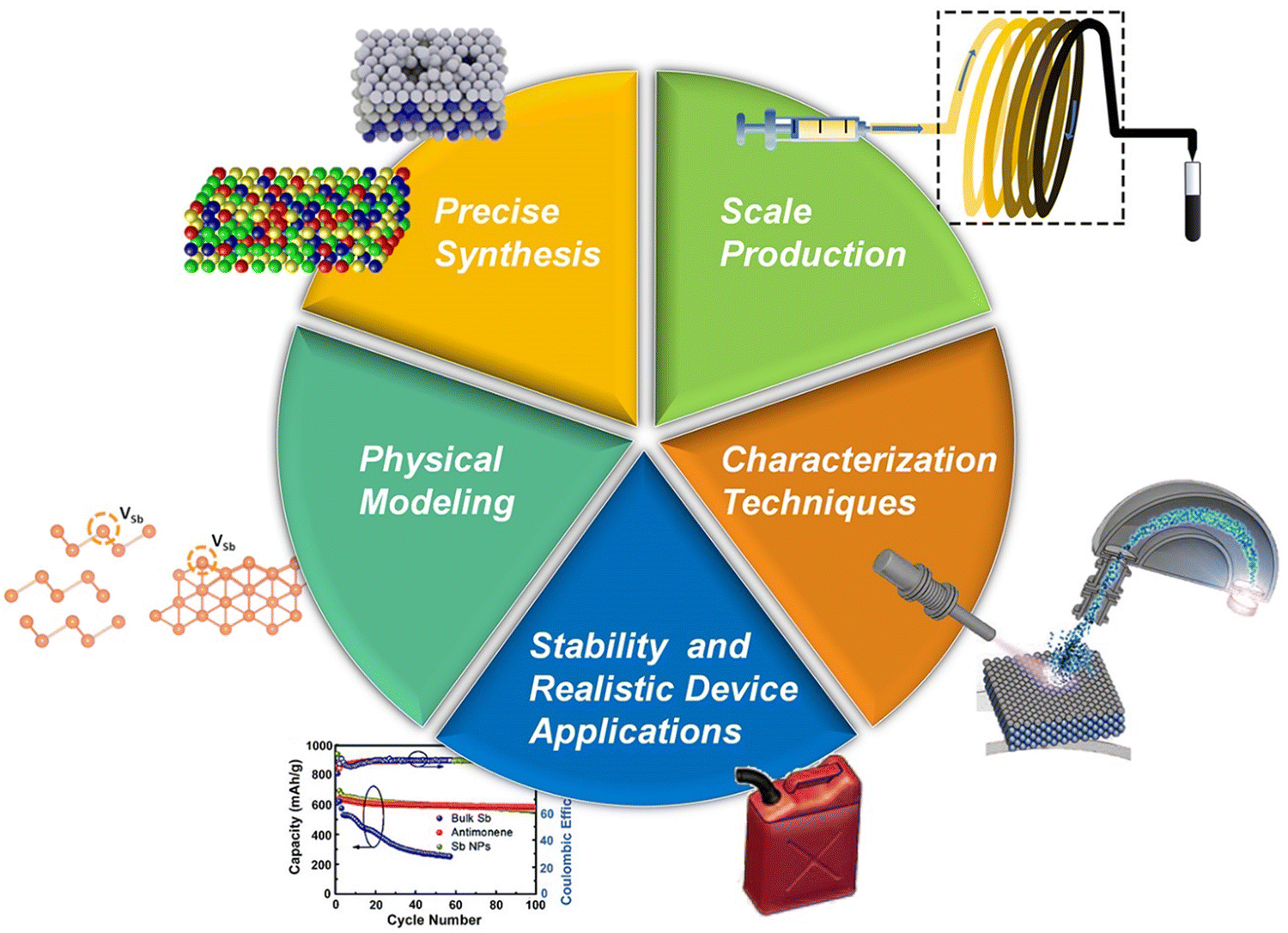 | ||
| Fig. 16 Outlook and potential research directions for metallene-related materials. Reproduced from ref. 80 with permission from AAAS. Copyright 2017. Reproduced from ref. 81 with permission from American Chemical Society. Copyright 2020. Reproduced from ref. 103 with permission from Elsevier. Copyright 2020. Reproduced from ref. 106 with permission from Wiley-VCH. Copyright 2019. Reproduced from ref. 107 with permission from the Royal Society of Chemistry. Copyright 2019. | ||
5.1. Precision synthesis control
Despite the successful synthesis of metallenes with different variations in terms of thickness, composition, lattice constants, and porosity, precise control over their synthesis at an atomic scale is still challenging due to the difficulty of high-level manipulation with the consideration of anisotropic growth of metals for maintaining the 2D morphology with atomic thickness. This precision in terms of synthesis control includes but is not limited to: (1) downscaling thickness to a new limit (sub-nanometer or even monolayer thickness) with a freestanding and stable structure, (2) generation of anisotropic strain over the surface, (3) precise elemental distribution in multielement metallenes, and (4) new crystal phases such as body-centered cubic (bcc) or orthorhombic structures with atomic thickness. In general, all the parameters associated with metallenes need to be precisely controlled and optimized in order to meet the requirements of electrocatalysis for various energy conversions.5.2. Characterization methods
Although great efforts have been made in the controlled synthesis of numerous metallenes by the bottom-up growth, the formation mechanism of these unique 2D metals still needs to be fully understood using both experimental tools and theoretical simulations. Given this, high-level characterization techniques are required for the in-depth investigation of the formation process from nucleation to anisotropic growth of metallenes. Thanks to the advancement of in situ characterization tools including in situ TEM, XRD, Raman, and XAS, different formation mechanisms will be revealed for the guidance and prediction of synthesis. Moreover, the delicate nature of metallenes typically leads to difficulties during characterization of the atomic structures by using conventional tools. For example, the high sensitivity of metallenes to the electron beams make them susceptible to falling apart when observed by TEM. This electron beam instability of metallenes needs to be taken into consideration especially when characterizing metallenes composed of solution alloys. In particular, to reveal the elemental distribution over the metallenes, their ultrathin nature requires an elongated time to collect a sufficient EDS signal, which leads to potentially aggravated electron beam-induced structural and even chemical deviation. This issue can be potentially addressed by using cryo-electron microscopy. In addition, the thermodynamic unfavorable structure is more susceptible to go through structural changes during their application in electrochemical and practical applications. Therefore, it is essentially important to develop new in situ characterization tools for observing these possible evolutions in different applications of metallenes.5.3. Scalable production
One challenge for most energy-related applications is to produce metallenes in large quantities without the compromise of control over thickness, composition, surface facets, and porosity. In the bottom-up synthesis by wet-chemical approaches, a typical strategy for increasing the productivity is to increase the volume of the reaction mixture. For example, by increasing the reaction volume from 5 mL to over 200 mL, the yield of PdMo metallene can also be increased by 40 times with a tight control over various parameters.17 However, the intrinsic thermal and compositional inhomogeneity over a large volume makes it highly challenging to obtain metallenes with high quality when the reaction volume is further scaled up. Therefore, other alternative approaches need to be developed to ensure the anisotropic growth of metallenes. For example, continuous-flow reactors have been used to address the inhomogeneity issue associated with the reaction volume by dividing the reaction mixture into droplets, plugs, or flow with a millimeter scale diameter for maintaining the homogeneity of the reaction solution.105,106 This new technique is able to achieve well-controlled reaction parameters for the scalable generation of nanomaterials without compromising their quality.5.4. Physical modeling
Physical modeling is fundamental for new structures to reveal their importance in various applications. However, relevant studies on metallene-related materials are still in the initial stage. As demonstrated in Fig. 1B, the elements involved in metallenes in the periodic table achieved by either experiments or theoretical calculations are still limited. So far, the expansion of theoretical modelling of 2D metal materials with atomic thickness is important to make this class of materials become more attractive to different communities for potential applications including electronics, optics, catalysis, and biomedicines.5.5. Stability and realistic device applications
Although progress in the synthesis and utilization of metallenes as electrocatalysts has recently been made, a number of challenges still need to be addressed before this class of nanomaterials can be used in real applications. Indeed, many of the electrocatalytic applications were merely proof-of-concept and performed in a laboratory. The cost, processability, and scale-up feasibility of metallenes all need to be taken into account for applications in realistic devices. Additionally, most of the metallenes might lack long-term stability and contamination resistance in these practical applications, which can be potentially addressed by oriented assembly of this class of materials to make them robust and functional in realistic devices. Therefore, there is still a long way to go before this unique class of 2D metals can be used in real-life energy conversion, especially when the operation conditions are harsh.Conflicts of interest
There are no conflicts to declare.Acknowledgements
This work was supported by the U.S. Department of Energy, Office of Science, Basic Energy Sciences under award DE-SC0019019, the Camille Dreyfus Teacher-Scholar Award, and the Norman Hackerman Award in Chemical Research by the Welch Foundation.Notes and references
- C. Tan, X. Cao, X.-J. Wu, Q. He, J. Yang, X. Zhang, J. Chen, W. Zhao, S. Han and G.-H. Nam, Chem. Rev., 2017, 117, 6225–6331 CrossRef CAS.
- H. Zhang, ACS Nano, 2015, 9, 9451–9469 CrossRef CAS.
- Z. Fang, Q. Xing, D. Fernandez, X. Zhang and G. Yu, Nano Res., 2020, 13, 1179–1190 CrossRef.
- Y. Zhu, L. Peng, Z. Fang, C. Yan, X. Zhang and G. Yu, Adv. Mater., 2018, 30, 1706347 CrossRef PubMed.
- F. Bonaccorso, L. Colombo, G. Yu, M. Stoller, V. Tozzini, A. C. Ferrari, R. S. Ruoff and V. Pellegrini, Science, 2015, 347, 1246501 CrossRef PubMed.
- L. Peng, Y. Zhu, H. Li and G. Yu, Small, 2016, 12, 6183–6199 CrossRef CAS PubMed.
- L. Peng, Y. Zhu, D. Chen, R. S. Ruoff and G. Yu, Adv. Energy Mater., 2016, 6, 1600025 CrossRef.
- C. Tang and S.-Z. Qiao, Matter, 2019, 1, 1454–1455 CrossRef.
- Y. Chen, Z. Fan, Z. Zhang, W. Niu, C. Li, N. Yang, B. Chen and H. Zhang, Chem. Rev., 2018, 118, 6409–6455 CrossRef CAS PubMed.
- P. Prabhu and J.-M. Lee, Chem. Soc. Rev., 2021, 50, 6700–6719 RSC.
- Y. Liu, K. N. Dinh, Z. Dai and Q. Yan, ACS Mater. Lett., 2020, 2, 1148–1172 CrossRef CAS.
- H. Yu, T. Zhou, Z. Wang, Y. Xu, X. Li, L. Wang and H. Wang, Angew. Chem., Int. Ed., 2021, 60, 12027–12031 CrossRef CAS.
- L. Wang, Z. Zeng, W. Gao, T. Maxson, D. Raciti, M. Giroux, X. Pan, C. Wang and J. Greeley, Science, 2019, 363, 870–874 CrossRef CAS.
- K. Deng, T. Zhou, Q. Mao, S. Wang, Z. Wang, Y. Xu, X. Li, H. Wang and L. Wang, Adv. Mater., 2022, 34, 2110680 CrossRef CAS.
- H. Duan, N. Yan, R. Yu, C.-R. Chang, G. Zhou, H.-S. Hu, H. Rong, Z. Niu, J. Mao, H. Asakura, T. Tanaka, P. Dyson, J. Li and Y. Li, Nat. Commun., 2014, 5, 1–8 Search PubMed.
- L. Zhao, C. Xu, H. Su, J. Liang, S. Lin, L. Gu, X. Wang, M. Chen and N. Zheng, Adv. Sci., 2015, 2, 1500100 CrossRef.
- M. Luo, Z. Zhao, Y. Zhang, Y. Sun, Y. Xing, F. Lv, Y. Yang, X. Zhang, S. Hwang, Y. Qin, J. Ma, F. Lin, D. Su, G. Lu and S. Guo, Nature, 2019, 574, 81–85 CrossRef CAS.
- A. Janssen, Q. N. Nguyen and Y. Xia, Angew. Chem., Int. Ed., 2021, 133, 12300–12311 CrossRef.
- Z. Li, L. Zhai, Y. Ge, Z. Huang, Z. Shi, J. Liu, W. Zhai, J. Liang and H. Zhang, Natl. Sci. Rev., 2022, 9, nwab142 CrossRef CAS.
- W. Zhu, L. Zhang, P. Yang, C. Hu, Z. Luo, X. Chang, Z. Zhao and J. Gong, Angew. Chem., Int. Ed., 2018, 57, 11544–11548 CrossRef CAS.
- D. Xu, Y. Liu, S. Zhao, Y. Lu, M. Han and J. Bao, Chem. Commun., 2017, 53, 1642–1645 RSC.
- S. Gao, Y. Lin, X. Jiao, Y. Sun, Q. Luo, W. Zhang, D. Li, J. Yang and Y. Xie, Nature, 2016, 529, 68–71 CrossRef CAS PubMed.
- X. Mu, J. Gu, F. Feng, Z. Xiao, C. Chen, S. Liu and S. Mu, Adv. Sci., 2021, 8, 2002341 CrossRef CAS.
- F. Lv, B. Huang, J. Feng, W. Zhang, K. Wang, N. Li, J. Zhou, P. Zhou, W. Yang, Y. Du, D. Su and S. Guo, Natl. Sci. Rev., 2021, 8, nwab019 CrossRef CAS PubMed.
- X. Li, P. Shen, Y. Luo, Y. Li, Y. Guo, H. Zhang and K. Chu, Angew. Chem., Int. Ed., 2022, 61, e202205923 CAS.
- J. Fan, J. Wu, X. Cui, L. Gu, Q. Zhang, F. Meng, B.-H. Lei, D. J. Singh and W. Zheng, J. Am. Chem. Soc., 2020, 142, 3645–3651 CrossRef CAS.
- J. Lai, F. Lin, Y. Tang, P. Zhou, Y. Chao, Y. Zhang and S. Guo, Adv. Energy Mater., 2019, 9, 1800684 CrossRef.
- J. Jiang, W. Ding, W. Li and Z. Wei, Chem, 2020, 6, 431–447 CAS.
- A. Funatsu, H. Tateishi, K. Hatakeyama, Y. Fukunaga, T. Taniguchi, M. Koinuma, H. Matsuura and Y. Matsumoto, Chem. Commun., 2014, 50, 8503–8506 RSC.
- J. Zhao, Q. Deng, A. Bachmatiuk, G. Sandeep, A. Popov, J. Eckert and M. H. Rümmeli, Science, 2014, 343, 1228–1232 CrossRef CAS.
- X. Huang, S. Li, Y. Huang, S. Wu, X. Zhou, S. Li, C. L. Gan, F. Boey, C. A. Mirkin and H. Zhang, Nat. Commun., 2011, 2, 1–6 Search PubMed.
- L. Tao, M. Sun, Y. Zhou, M. Luo, F. Lv, M. Li, Q. Zhang, L. Gu, B. Huang and S. Guo, J. Am. Chem. Soc., 2022, 144, 10582–10590 CrossRef CAS.
- W. Zhang, Y. Hu, L. Ma, G. Zhu, P. Zhao, X. Xue, R. Chen, S. Yang, J. Ma, J. Liu and Z. Jin, Nano Energy, 2018, 53, 808–816 CrossRef CAS.
- F. Zhang, J. He, Y. Xiang, K. Zheng, B. Xue, S. Ye, X. Peng, Y. Hao, J. Lian, P. Zeng, J. Qu and J. Song, Adv. Mater., 2018, 30, 1803244 CrossRef.
- Y. Li, J. Chen, J. Huang, Y. Hou, L. Lei, W. Lin, Y. Lian, X. Zhonghua, H. Yang and Z. Wen, Chem. Commun., 2019, 55, 10884–10887 RSC.
- J. Yin, Z. Yin, J. Jin, M. Sun, B. Huang, H. Lin, Z. Ma, M. Muzzio, M. Shen, C. Yu, H. Zhang, Y. Peng, P. Xi, C. Yan and S. Sun, J. Am. Chem. Soc., 2021, 143, 15335–15343 CrossRef CAS.
- X. Wang, J. He, B. Zhou, Y. Zhang, J. Wu, R. Hu, L. Liu, J. Song and J. Qu, Angew. Chem., Int. Ed., 2018, 57, 8668–8673 CrossRef CAS PubMed.
- V. Kochat, A. Samanta, Y. Zhang, S. Bhowmick, P. Manimunda, S. A. S. Asif, A. S. Stender, R. Vajtai, A. K. Singh, C. S. Tiwary and P. M. Ajayan, Sci. Adv., 2018, 4, e1701373 CrossRef.
- X. Wang, C. Wang, C. Chen, H. Duan and K. Du, Nano Lett., 2019, 19, 4560–4566 CrossRef CAS.
- F. Y. A. O. Elnabawy, R. Schimmenti, P. Song, J. Wang, Z. Peng, S. Yao, R. Deng, S. Song, Y. Lin, M. Mavrikakis and W. Xu, Nat. Commun., 2020, 11, 1–8 CrossRef.
- H. Liu, S. Han, Y. Zhao, Y. Zhu, X. Tian, J. Zeng, J. Jiang, B. Xia and Y. Chen, J. Mater. Chem. A, 2018, 6, 3211–3217 RSC.
- Y. Sun, T. Jiang, J. Duan, L. Jiang, X. Hu, H. Zhao, J. Zhu, S. Chen and X. Wang, ACS Catal., 2020, 10, 11371–11379 CrossRef CAS.
- C. Cao, D. D. Ma, J. F. Gu, X. Xie, G. Zeng, X. Li, S. G. Han, Q. L. Zhu, X. T. Wu and Q. Xu, Angew. Chem., Int. Ed., 2020, 59, 15014–15020 CrossRef CAS PubMed.
- M. Zhang, W. Wei, S. Zhou, D. Ma, A. Cao, X. Wu and Q. Zhu, Energy Environ. Sci., 2021, 14, 4998–5008 RSC.
- W. Ma, J. Bu, Z. Liu, C. Yan, Y. Yao, N. Chang, H. Zhang, T. Wang and J. Zhang, Adv. Funct. Mater., 2021, 31, 2006704 CrossRef CAS.
- C. Peng, X. Wu, G. Zeng and Q. Zhu, Chem. – Asian J., 2021, 16, 1539–1544 CrossRef CAS PubMed.
- V. Georgakilas, J. N. Tiwari, K. C. Kemp, J. A. Perman, A. B. Bourlinos, K. S. Kim and R. Zboril, Chem. Rev., 2016, 116, 5464–5519 CrossRef CAS.
- X. Chia, A. Y. S. Eng, A. Ambrosi, S. M. Tan and M. Pumera, Chem. Rev., 2015, 115, 11941–11966 CrossRef CAS PubMed.
- J. Yu, Q. Wang, D. O'Hare and L. Sun, Chem. Soc. Rev., 2017, 46, 5950–5974 RSC.
- Q.-Q. Yang, R.-T. Liu, C. Huang, Y.-F. Huang, L.-F. Gao, B. Sun, Z.-P. Huang, L. Zhang, C.-X. Hu and Z.-Q. Zhang, Nanoscale, 2018, 10, 21106–21115 RSC.
- K. Fukuda, J. Sato, T. Saida, W. Sugimoto, Y. Ebina, T. Shibata, M. Osada and T. Sasaki, Inorg. Chem., 2013, 52, 2280–2282 CrossRef CAS.
- C. Cao, Q. Xu and Q.-L. Zhu, Chem Cat., 2022, 2(4), 693–723 Search PubMed.
- K. Zhang, Y. He, R. Guo, W. Wang, Q. Zhan, R. Li, T. He, C. Wu and M. Jin, ACS Energy Lett., 2022, 7, 3329–3336 CrossRef CAS.
- M. Che, Cat. Today, 2013, 218, 162–171 CrossRef.
- B. Hammer and J. K. Nørskov, Advances in catalysis, Elsevier, 2000, vol. 45, pp. 71–129 Search PubMed.
- P. Liu, R. Qin, G. Fu and N. Zheng, J. Am. Chem. Soc., 2017, 139, 2122–2131 CrossRef CAS PubMed.
- V. R. Stamenkovic, B. Fowler, B. S. Mun, G. Wang, P. N. Ross, C. A. Lucas and N. M. Markovic, Science, 2007, 315, 493–497 CrossRef CAS PubMed.
- Y. Xia, X. Xia and H.-C. Peng, J. Am. Chem. Soc., 2015, 137, 7947–7966 CrossRef CAS PubMed.
- T. H. Yang, Y. Shi, A. Janssen and Y. Xia, Angew. Chem., Int. Ed., 2020, 59, 15378–15401 CrossRef CAS PubMed.
- D. Xu, X. Liu, H. Lv, Y. Liu, S. Zhao, M. Han, J. Bao, J. He and B. Liu, Chem. Sci., 2018, 9, 4451–4455 RSC.
- W. Rootsaert and W. Sachtler, Z. Phys. Chem., 1960, 26, 16–26 CrossRef CAS.
- A.-X. Yin, W.-C. Liu, J. Ke, W. Zhu, J. Gu, Y.-W. Zhang and C.-H. Yan, J. Am. Chem. Soc., 2012, 134, 20479–20489 CrossRef CAS PubMed.
- T. Bligaard and J. K. Nørskov, Electrochim. Acta, 2007, 52, 5512–5516 CrossRef CAS.
- S. Huang, S. Lu, S. Gong, Q. Zhang, F. Duan, H. Zhu, H. Gu, W. Dong and M. Du, ACS Nano, 2021, 16, 522–532 CrossRef PubMed.
- N. Yang, Z. Zhang, B. Chen, Y. Huang, J. Chen, Z. Lai, Y. Chen, M. Sindoro, A. L. Wang and H. Cheng, Adv. Mater., 2017, 29, 1700769 CrossRef.
- Q. Yang, L. Shi, B. Yu, J. Xu, C. Wei, Y. Wang and H. Chen, J. Mater. Chem. A, 2019, 7, 18846–18851 RSC.
- Y. Yao, Z. Huang, P. Xie, S. D. Lacey, R. J. Jacob, H. Xie, F. Chen, A. Nie, T. Pu and M. Rehwoldt, Science, 2018, 359, 1489–1494 CrossRef CAS.
- D. Wu, K. Kusada, T. Yamamoto, T. Toriyama, S. Matsumura, S. Kawaguchi, Y. Kubota and H. Kitagawa, J. Am. Chem. Soc., 2020, 142, 13833–13838 CrossRef CAS.
- G. Feng, F. Ning, J. Song, H. Shang, K. Zhang, Z. Ding, P. Gao, W. Chu and D. Xia, J. Am. Chem. Soc., 2021, 143, 17117–17127 CrossRef CAS PubMed.
- M. Mavrikakis, B. Hammer and J. K. Nørskov, Phys. Rev. Lett., 1998, 81, 2819 CrossRef.
- M. Luo, Y. Yang, Y. Sun, Y. Qin, C. Li, Y. Li, M. Li, S. Zhang, D. Su and S. Guo, Mater. Today, 2019, 23, 45–56 CrossRef CAS.
- M. Xie, B. Zhang, Z. Jin, P. Li and G. Yu, ACS Nano, 2022, 16, 13715–13727 CrossRef CAS.
- F. Calle-Vallejo, J. Tymoczko, V. Colic, Q. H. Vu, M. D. Pohl, K. Morgenstern, D. Loffreda, P. Sautet, W. Schuhmann and A. S. Bandarenka, Science, 2015, 350, 185–189 CrossRef CAS.
- F. Lin, F. Lv, Q. Zhang, H. Luo, K. Wang, J. Zhou, W. Zhang, W. Zhang, D. Wang, L. Gu and S. Guo, Adv. Mater., 2022, 2202084 CrossRef CAS.
- H. Cheng, N. Yang, G. Liu, Y. Ge, J. Huang, Q. Yun, Y. Du, C. Sun, B. Chen, J. Liu and H. Zhang, Adv. Mater., 2020, 32, 1902964 CrossRef CAS.
- B. C. Steele and A. Heinzel, Materials for sustainable energy: a collection of peer-reviewed research and review articles from Nature Publishing Group, World Scientific, 2011, pp. 224–231 Search PubMed.
- M. K. Debe, Nature, 2012, 486, 43–51 CrossRef CAS PubMed.
- C. Song and J. Zhang, PEM fuel cell electrocatalysts and catalyst layers: fundamentals and applications, Springer Science & Business Media, 2008 Search PubMed.
- M. Xie, Z. Lyu, R. Chen, M. Shen, Z. Cao and Y. Xia, J. Am. Chem. Soc., 2021, 143, 8509–8518 CrossRef CAS PubMed.
- Z. W. Seh, J. Kibsgaard, C. F. Dickens, I. Chorkendorff, J. K. Nørskov and T. F. Jaramillo, Science, 2017, 355, eaad4998 CrossRef PubMed.
- Z. Liu, Z. Zhao, B. Peng, X. Duan and Y. Huang, J. Am. Chem. Soc., 2020, 142, 17812–17827 CrossRef CAS.
- X. Mu, J. Gu, F. Feng, Z. Xiao, C. Chen, S. Liu and S. Mu, Adv. Sci., 2021, 8, 2002341 CrossRef CAS.
- C. Li, Y. Xu, S. Liu, S. Yin, H. Yu, Z. Wang, X. Li, L. Wang and H. Wang, ACS Sus. Chem. & Engi., 2019, 7, 15747–15754 Search PubMed.
- J. Fan, X. Cui, S. Yu, L. Gu, Q. Zhang, F. Meng, Z. Peng, L. Ma, J.-Y. Ma and K. Qi, ACS Nano, 2019, 13, 12987–12995 CrossRef CAS PubMed.
- C. W. A. Chan, A. H. Mahadi, M. M.-J. Li, E. C. Corbos, C. Tang, G. Jones, W. C. H. Kuo, J. Cookson, C. M. Brown and P. T. Bishop, Nat. Commun., 2014, 5, 1–10 Search PubMed.
- J. Li, J. Chen, Q. Wang, W.-B. Cai and S. Chen, Chem. Mater., 2017, 29, 10060–10067 CrossRef CAS.
- K. A. Kuttiyiel, K. Sasaki, Y. Choi, D. Su, P. Liu and R. R. Adzic, Nano Lett., 2012, 12, 6266–6271 CrossRef CAS.
- L. Chen, L. Lu, H. Zhu, Y. Chen, Y. Huang, Y. Li and L. Wang, Nat. Commun., 2017, 8, 1–9 CrossRef CAS.
- C. F. Shih, T. Zhang, J. Li and C. Bai, Joule, 2018, 2, 1925–1949 CrossRef CAS.
- Y. Kang, J. B. Pyo, X. Ye, T. R. Gordon and C. B. Murray, ACS Nano, 2012, 6, 5642–5647 CrossRef CAS PubMed.
- M. K. Kabiraz, J. Kim, W.-J. Lee, B. Ruqia, H. C. Kim, S.-U. Lee, J.-R. Kim, S.-M. Paek, J. W. Hong and S.-I. Choi, Chem. Mater., 2019, 31, 5663–5673 CrossRef CAS.
- Y. Shi, Z. Lyu, Z. Cao, M. Xie and Y. Xia, Angew. Chem., Int. Ed., 2020, 59, 19129–19135 CrossRef CAS.
- R. Guo, K. Zhang, Y. Liu, Y. He, C. Wu and M. Jin, J. Mater. Chem. A, 2021, 9, 6196–6204 RSC.
- Q. Yun, Q. Lu, C. Li, B. Chen, Q. Zhang, Q. He, Z. Hu, Z. Zhang, Y. Ge and N. Yang, ACS Nano, 2019, 13, 14329–14336 CrossRef CAS PubMed.
- Y. Qin, W. Zhang, F. Wang, J. Li, J. Ye, X. Sheng, C. Li, X. Liang, P. Liu and X. Wang, Angew. Chem., Int. Ed., 2022, 134, e202200899 Search PubMed.
- C. Tang, N. Zhang, Y. Ji, Q. Shao, Y. Li, X. Xiao and X. Huang, Nano Lett., 2019, 19, 1336–1342 CrossRef CAS PubMed.
- X. Ai, X. Zou, H. Chen, Y. Su, X. Feng, Q. Li, Y. Liu, Y. Zhang and X. Zou, Angew. Chem., Int. Ed., 2020, 59, 3961–3965 CrossRef CAS PubMed.
- D. Gao, R. M. Arán-Ais, H. S. Jeon and B. Roldan Cuenya, Nat. Cat., 2019, 2, 198–210 CrossRef CAS.
- G. Wang, J. Chen, Y. Ding, P. Cai, L. Yi, Y. Li, C. Tu, Y. Hou, Z. Wen and L. Dai, Chem. Soc. Rev., 2021, 50, 4993–5061 RSC.
- B. H. R. Suryanto, H. Du, D. Wang, J. Chen, A. N. Simonov and D. R. MacFarlane, Nat. Cat., 2019, 2, 290–296 CrossRef CAS.
- W. Xu, G. Fan, J. Chen, J. Li, L. Zhang, S. Zhu, X. Su, F. Cheng and J. Chen, Angew. Chem., Int. Ed., 2020, 59, 3511–3516 CrossRef CAS.
- Z. Wang, H. Zhao, J. Liu, D. Zhang, X. Wu, N. Nie, D. Wu, W. Xu, J. Lai and L. Wang, Chem. Eng. J., 2022, 450, 137951 CrossRef CAS.
- Z. Zhao, C. Choi, S. Hong, H. Shen, C. Yan, J. Masa, Y. Jung, J. Qiu and Z. Sun, Nano Energy, 2020, 78, 105368 CrossRef CAS.
- D. Zhang, X. Cui, L. Liu, Y. Xu, J. Zhao, J. Han and W. Zheng, ACS Appl. Mater. Interfaces, 2021, 13, 21582–21592 CrossRef CAS.
- G. Niu, A. Ruditskiy, M. Vara and Y. Xia, Chem. Soc. Rev., 2015, 44, 5806–5820 RSC.
- R. Chen, Z. Cao, Z. Lyu, M. Xie, Y. Shi and Y. Xia, ChemNanoMat, 2019, 5, 599–605 CrossRef CAS.
- Y. Gao, W. Tian, C. Huo, K. Zhang, S. Guo, S. Zhang, X. Song, L. Jiang, K. Huo and H. Zeng, J. Mater. Chem. A, 2019, 7, 3238–3243 RSC.
| This journal is © The Royal Society of Chemistry 2023 |