
 Open Access Article
 This Open Access Article is licensed under a Creative Commons Attribution-Non Commercial 3.0 Unported Licence
A comprehensive insight into deep-level defect engineering in antimony chalcogenide solar cells†
Swapnil
Barthwal
,
Siddhant
Singh
,
Abhishek K.
Chauhan
,
Nimitha S.
Prabhu
,
Akila G.
Prabhudessai
 and
K.
Ramesh
*
and
K.
Ramesh
*
Department of Physics, Indian Institute of Science, Bengaluru-560012, Karnataka, India. E-mail: kramesh@iisc.ac.in
First published on 13th October 2023
Abstract
Antimony chalcogenides (Sb2X3, X = S and Se) are intriguing materials for the fabrication of next-generation, flexible/wearable, lightweight, and tandem photovoltaic (PV) devices. Recently, the power conversion efficiency (PCE) of 10.75% and 11.66% has been demonstrated in (single junction) Sb2X3 and Sb2X3/Si (tandem) solar cells, respectively. However, the inevitable presence (>1016 cm−3) of deep-level defects (especially SbS and SbSe antisites) induces Fermi-level (EF) pinning, accelerates Shockley–Read–Hall (SRH) recombination, and shortens the carrier lifetime. Unambiguously, these defects result in sluggish charge transport and high open-circuit voltage (VOC) deficits in the corresponding Sb2X3 solar cells. Therefore, a comprehensive understanding of the deep-level defects and their passivation strategies can be instrumental in reducing the VOC deficits and boosting the PCE values. In this regard, the present review highlights the expanding toolbox of defect-engineering strategies for Sb2X3 films, laying a solid foundation for improving the PCE of Sb2X3 solar cells.
 Swapnil Barthwal | Swapnil Barthwal completed his MTech (Solid State Materials) from the Indian Institute of Technology, Delhi, in 2019. Currently, he is working as a Project Fellow in the Department of Physics, Indian Institute of Science, Bengaluru. His research work is focused on understanding and regulating the point defects in Antimony Chalcogenide (Sb2X3) thin films to exercise greater control of the carrier-transport dynamics and PV performance in Sb2X3 solar cells. |
 Siddhant Singh | Siddhant Singh graduated in Physical Sciences from University of Delhi, in 2018. He completed his Master's in Physics, from the National Institute of Technology Surathkal, Karnataka in 2021. Subsequently, he joined the Photovoltaics Group for his doctoral research under the supervision of Dr K. Ramesh (Principal Research Scientist) at the Indian Institute of Science, Bengaluru. His research interests include the fabrication and investigation of optoelectronic devices based on solution-processed perovskite single crystals and thin films. |
 Abhishek K. Chauhan | Abhishek Kumar Chauhan is currently working as a Research Associate at the Department of Physics, Indian Institute of Science, Bengaluru, India. He earned his PhD in 2022 under the guidance of Dr Pankaj Kumar (Principal Scientist, National Physical Laboratory, New Delhi, India). His doctoral work was focused on the development of perovskite-based solar cells and involved an in-depth study of their degradation mechanisms. In his current role, he continues to explore and advance the field of perovskite-chalcogenide-based solar cells. |
 Nimitha S. Prabhu | Nimitha S. Prabhu gained her PhD at the Manipal Institute of Technology, Manipal, India in 2023, working on the effects of gamma-irradiation on rare-earth-doped oxide glasses. Subsequently, he joined the Amorphous Semiconductors Group of Dr K. Ramesh (Principal Research Scientist) at the Indian Institute of Science, Bengaluru, India as a Research Associate. Her research interests include rare-earth-doped oxide and chalcogenide glasses, gamma dosimetry, and thin-film solar cells. |
 Akila G. Prabhudessai | Akila G. Prabhudessai earned her PhD from Jadavpur University, Kolkata in 2022, working on the synthesis of multi-component chalcogenide glasses for mid-infrared and electrical applications. Currently, she is working as a Research Associate in Dr K. Ramesh's group, Department of Physics, Indian Institute of Science, Bengaluru. Her research interests include the synthesis, purification and impedance and optical spectroscopy of chalcogenide glasses. |
 K. Ramesh | Dr Ramesh Karuppannan is working as a Principal Research Scientist at the Indian Institute of Science, Bangalore, India. He completed his BSc (Physics) and MSc (Physics) at the Bharathidasan University, Trichy, India. He obtained his Doctorate in 1999 from the Indian Institute of Science, Bengaluru, India. His main research areas are structural relaxation in chalcogenide glasses, IR-transmitting materials, phase-change memory materials, carbon nitrides, pressure-induced phase transitions, and photovoltaic materials based on SnS and perovskites. |
1. Introduction
The unique quasi-one-dimensional (Q-1D) crystal structure, economical fabrication, and power conversion efficiency (PCE) evolution have stimulated significant scientific and industrial interest towards antimony chalcogenide (Sb2X3, X= S, Se) photovoltaics (PV). Furthermore, Sb2X3 has the advantages of earth-abundance, low eco-toxicity, high absorption coefficient (>105 cm−1), low Urbach energy (∼30 meV), low exciton binding energy, readily tunable bandgap (Eg ∼ 1.1–1.7 eV, depending on the Se/S ratio), superior physicochemical stability, balanced (ambipolar) charge transport, and ultra-flexibility, satisfying most of the requirements of an ideal PV material.1–7 Due to the rapid progress in film deposition strategies and composition and device engineering, PCE values of 8.00%,8 10.57%,9 and 10.75%10 have been reported for Sb2S3, Sb2Se3, and Sb2(S,Se)3 solar cells, respectively. Recently, a PCE of 11.66% was demonstrated in an Sb2(S,Se)3/Si tandem solar cell.11 Sb2S3 (Eg ∼ 1.7 eV) and Sb2Se3 (Eg ∼ 1.1 eV) are promising materials for the fabrication of the top-cell and bottom-cell in tandem solar cells, respectively.12–15 In addition to generic power production (terawatt levels), Sb2X3 solar cells are well suited for integration in futuristic, lightweight, flexible, and wearable electronic devices.15–18A comprehensive understanding of the defect-formation mechanism and control of defects via passivation strategies has been a cornerstone in the successful technological deployment of established semiconductor technologies. However, this profound understanding is limited in the case of Sb2X3 solar cells, which severely suffer from large open circuit voltage (VOC) deficits (>0.6 eV) owing to their high density of (electrically active) deep defects. These defects are localized in real space, dictate the carrier transport, and restrict the PCE of the corresponding devices from reaching the theoretical limit (∼30%).18,19
To date, various reviews have covered different critical aspects of Sb2X3 PV, with particular emphasis on presenting either a generic overview (of anisotropy, crystal-structure, band-structure, photophysical properties, deposition techniques, and recent advances),18,20–26 doping,27 device and interfacial engineering,19,28,29 or commercialization prospects,30 while the defect engineering aspect has largely remained unexplored. Recently, Wijesinghe et al.31 published a review emphasizing defect engineering in Sb2Se3 solar cells. However, to the best of our knowledge, the present review is unique, highlighting the origin of deep-level defects in Sb2X3 (covering Sb2S3, Sb2Se3, and Sb2(S,Se)3), their passivation strategies, and strategies for boosting their PCE beyond the state-of-the-art. This work is organized into five main sections. Firstly, we briefly elucidate the charge transport properties of Sb2X3 materials. Next, we summarize the defect engineering investigations, discussing the origin of deep-level defects and their influence on the performance of Sb2X3 solar cells. Subsequently, we present the engineering strategies for defect passivation and PCE improvement in Sb2X3 solar cells. Finally, we present a summary and technological outlook, outlining potential challenges and future research directions. We anticipate that this work will inspire the development of novel strategies for defect regulation in Sb2X3 films and solar cells, laying a solid foundation for improving their PCE.
2. Charge carrier dynamics in Sb2X3
Although the anisotropic structural and optoelectronic properties of Sb2X3 have been investigated comprehensively, there is no consensus on its charge-carrier dynamics, which critically affects the performance of Sb2X3 solar cells. Specifically, the nature of the carrier transport remains ambiguous, regarding if it is band-like or thermally activated hopping. Moon's group performed several time-resolved studies to understand the carrier dynamics involved in Sb2Se3 nanostructures.32 Time-resolved terahertz (tr-THz) spectroscopy revealed that the photoexcited carriers in Sb2Se3 undergo effective mobility loss within 30 ps owing to the carrier localization, while time-resolved photoluminescence (TRPL) suggested the recombination of photogenerated carriers in a lengthier (ns) time scale. Furthermore, the carrier localization was attributed to the soft/deformable and anharmonic crystal structure, strong electron–phonon coupling and carrier interaction with crystal distortions in Sb2Se3.33 Zhu's group conducted an in-depth investigation on the carrier dynamics in Sb2S3 single crystals and thin films via transient absorption spectroscopy (TAS).34 They concluded that the red-shifted PL (Stokes shift of 0.6 eV), picosecond carrier trapping, polarized trap emission, and hopping transport were strongly correlated with the intrinsic self-trapping of photogenerated carriers by lattice deformations in Sb2S3. The self-trapping model rationalizes the high VOC-deficits in Sb2S3 solar cells, pinning the upper limit of the VOC at 0.8 V and PCE at 16%. Grad et al.35 performed time-resolved two-photon photoemission experiments to study the photoexcited carrier dynamics in single-crystal Sb2S3. They proposed a model of self-trapping of free charge carriers by optical phonons and the formation of intrinsic traps. Consistent with the above-mentioned hypothesis, Tao et al. reported a Stokes-shifted (≈0.5 eV) broadband emission and (barrierless) ultrafast (≈20 ps) carrier self-trapping in Sb2Se3 and Sb2(S,Se)3, regardless of their crystallinity and stoichiometry.36To counter the proposed intrinsic self-trapping model, various studies revealed that carriers are localized by extrinsic (bulk and interface) defects. Yang's group investigated the anisotropic photoconductivity in Sb2Se3 single crystals via tr-THz spectroscopy.37 The temporal evolution of photoconductivity revealed that electron trapping resulted in a variation in photoconductivity anisotropy, which was accompanied by a decline in the photoconductivity magnitude, while electron–hole recombination only reduced the magnitude but did not affect the anisotropy. Photoconductivity decay and the accompanying anisotropy reversal revealed that at low pump intensities (relevant to the solar insolation), electron trapping outpaced charge recombination and dictated the photoconductivity dynamics. Leng's group investigated the charge carrier transfer and trap state localization process in Sb2Se3 films and heterostructures (CdS/Sb2Se3 and SnO2/Sb2Se3) via visible-pump terahertz-probe spectroscopy (VPTPS).38 In the case of the CdS/Sb2Se3 heterostructure, the band edge electron transfer time (∼50 ps) was almost double that for the trapping process (∼30 ps), revealing that the intrinsic trap-assisted carrier recombination dominates the loss mechanisms.
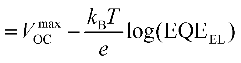
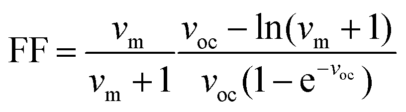
Walsh's group investigated the tendency of polaron-trapping and its effect on the charge-carrier transport in Sb2X3 using density functional theory (DFT) and Boltzmann transport calculations.6 The modeling of electron and hole polarons in Sb2X3 indicated the intrinsic formation of large polarons, in contrast to prior suggestions of small polarons (i.e., self-trapped carriers). As illustrated in Fig. 1(a), the isotopically averaged mobilities (for both electrons and holes) exceeded 10 cm2 V−1 s−1 at room temperature and declined with an increase in temperature, confirming the band-like transport in Sb2S3 and Sb2Se3. It was also revealed that the intrinsic mobility is limited by scattering from polar optical phonons at low and moderate defect densities. In the case of high charge defect concentrations (>1018 cm−3), impurity scattering dominated. Yang's group employed Tr-THz and TAS to investigate both the free and trapped carrier dynamics in Sb2Se3 films.39 The results revealed that the trapped carriers remain mobile and reach charge-collecting interfaces prior to recombination. Interestingly, in addition to free carriers, trapped carriers were also found to contribute to the photocurrent in Sb2Se3 solar cells, as schematically depicted in Fig. 1(d).
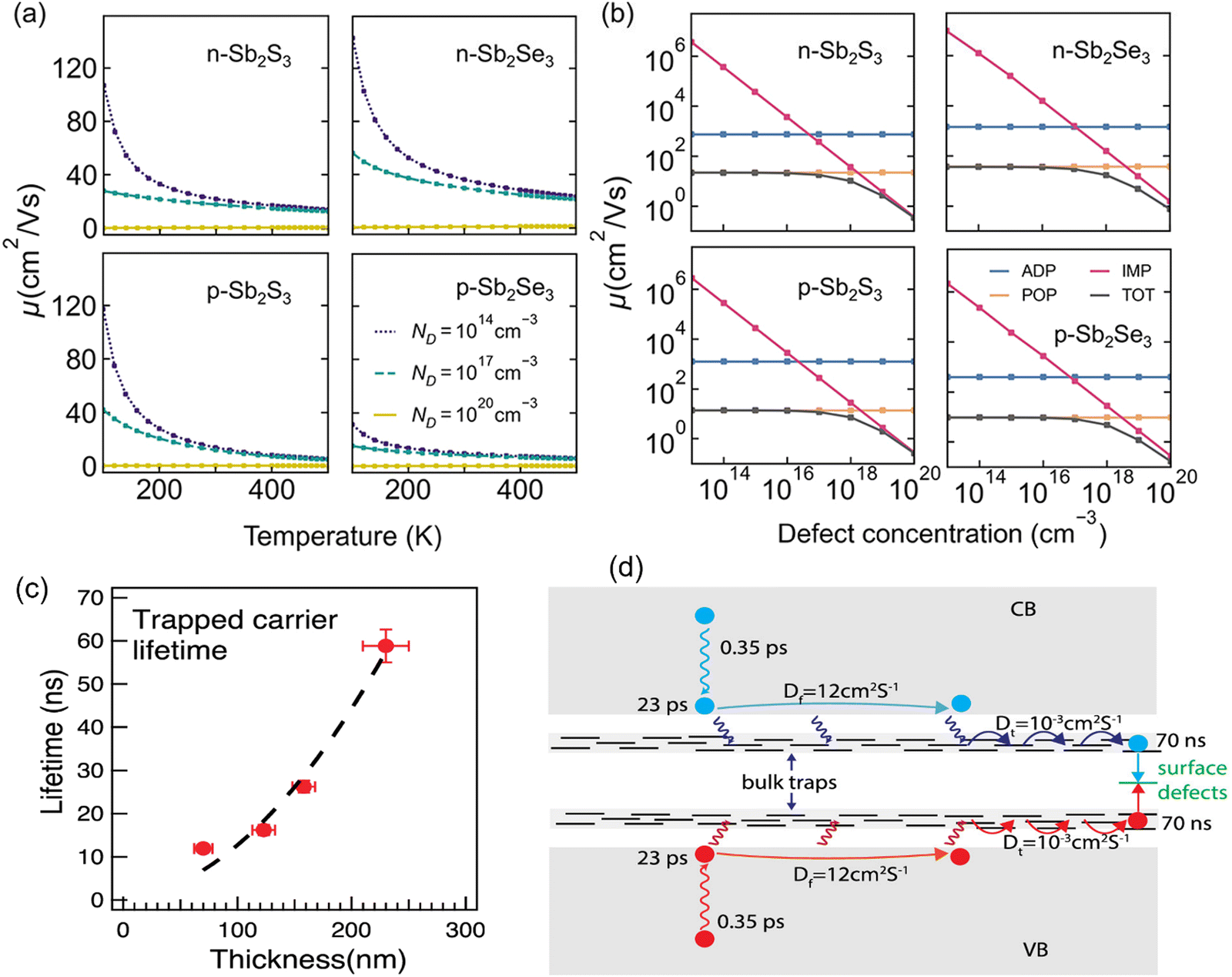 | ||
| Fig. 1 Calculated average mobility (μ) values for electrons and holes in Sb2S3 and Sb2Se3 as a function of (a) temperature and (b) defect concentration (ND). Calculated total (TOT) and component mobilities as a function of bulk defect concentration at 300 K. ADP, acoustic deformation potential; POP, polar optical phonon; and IMP, ionized impurity. Adapted under the guidelines of the Creative Commons CC BY license from ref. 6 Copyright 2022, the American Chemical Society. (c) Dependence of trapped carrier lifetime (τt) on film thickness. (d) Schematic illustration of the free and trapped charge carrier transport. The free carrier cooling (0.35 ps) and subsequent trapping (23 ps) time constants are shown. The trapped carriers hop among the bulk trap sites with a narrow energy distribution. Surface recombination leads to the depopulation of the trapped carriers. Adapted with permission from ref. 39 Copyright 2019, the American Chemical Society. | ||
Although Sb2S3 and Sb2Se3 are isomorphous and exhibit similar material properties, they exhibit minor differences in their electronic properties. Generally, Sb2S3 exhibits intrinsic to weakly n-type conductivity, in contrast to weakly p-type conductivity in Sb2Se3. Strong electron–phonon coupling-induced (intrinsic) self-trapping is prominent in Sb2S3, limiting the VOC and FF values in Sb2S3 solar cells. However, it is conceivable that there is ambiguity regarding the self-trapping in Sb2Se3 and Sb2(S,Se)3 and the extent to which it impedes carrier transport in these materials.35,40 The suppressed or non-existent self-trapping in Sb2Se3 and Sb2(S,Se)3 facilitates improved charge transport, which is reflected in their better device performance than their Sb2S3 counterparts (Table S1, ESI†). Notably, the upper limit of the VOC (∼0.8 eV) projected by the self-trapping model for Sb2S3 solar cells was experimentally reported by Maity et al.41 and Peng et al.42 In this regard, any further improvement in VOC will provide evidence for the validity and efficacy of this model. Engineering strategies to suppress electron–phonon coupling (such as stiffening the elastic properties by strain) can counter the ultrafast self-trapping in Sb2X3 films.
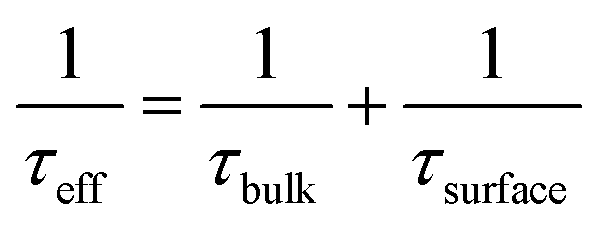
3. Defects in Sb2X3 materials and their implication in the performance of solar cells
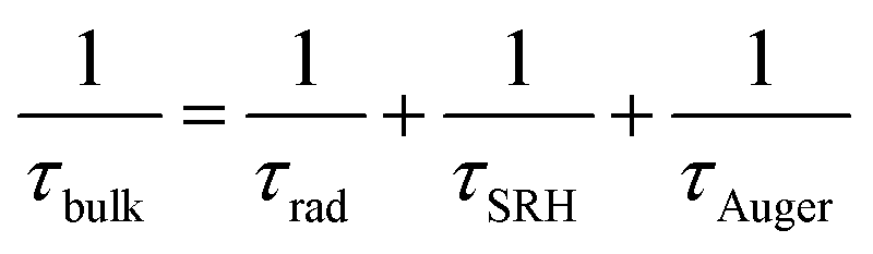
Computational and experimental studies on Sb2X3 thin films revealed the highly complicated and sensitive (to film deposition conditions) nature of defects. The following defects in Sb2X3 films dictate the performance of Sb2X3 solar cells: (1) intrinsic zero-dimensional (0D) defects, including vacancies, interstitials and antisites; (2) 0D defects caused by impurities (doped or permeable ions); and (3) 2D defects (grain boundaries, interfaces, and surface defects). In addition, defects in the transport layer and poor contact between the transport layer and electrodes also affect charge extraction, resulting in a higher series resistance (RS). Moreover, severe defects such as microcracks and scratches on the surface cause a rough surface topography, lowering the FF in devices. However, in this review, we focus on the point (0D) defects in the absorber layers. Point defects can be classified as deep or shallow, depending on whether the thermal activation energies for the electrons (Eth) are higher or lower than kBT (kB is the Boltzmann constant and T is the absolute temperature). Point defects with deep-energy levels are prone to tightly trapping free electrons and holes, resulting in defect-mediated Shockley–Read–Hall (SRH) recombination, and thus curtaining the average lifetime (τeff) of the charge carriers and VOC of PV devices. In contrast, shallow defects are benign and instrumental tools for regulating the carrier density and electrical conductivity. Solar energy conversion requires the photoinduced generation of long-lived charge carriers, which necessitate their separation and collection at the respective electrodes to generate a discernible VOC and JSC. Thus, mitigating all the possible charge carrier loss channels is indispensable for attaining excellent PCE values.38Suppressing the rate of trap-assisted SRH recombination enables devices to achieve higher VOC values before the JSC is canceled completely by recombination. The VOC can be formulated in terms of non-radiative voltage loss (ΔVNROC) from the maximum achievable voltage (ΔVNROC),43 as follows:
| VOC = VmaxOC − ΔVNROC | (1) |
 | (2) |
V OC and FF are closely related to the defect-assisted recombination losses caused by bulk traps and interface defects (improper energy-level alignment, lattice-mismatching, and dangling bonds). The FF of a solar cell is defined as the product of its current and voltage values at the maximum power output relative to the product of JSC and VOC. Therefore, the FF is strongly affected not only by the series and shunt resistance but also by carrier recombination (at the maximum power point conditions). The latter effect is well illustrated by the semiempirical expression, showing the dependency of FF on the diode ideality factor (η) and VOC,44 as follows:
 | (3) |
 | (4) |
vm = voc − ln(voc + 1 − ln![[thin space (1/6-em)]](https://www.rsc.org/images/entities/char_2009.gif) voc) voc) | (5) |
 | (6) |
 | (7) |
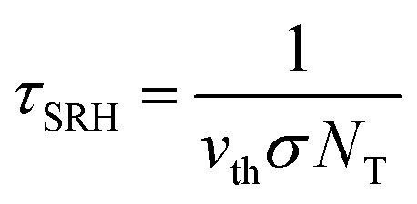
To intuitively assess the influence of individual types of deep-level defects on the device performance, the (σ·NT)−1 values are evaluated and compared. According to the trap-assisted-SRH recombination model, the τSRH value associated with a specific defect depends on the carrier thermal velocity (vth), capture cross section (σ), and trap density (NT), as follows:49,50
 | (8) |
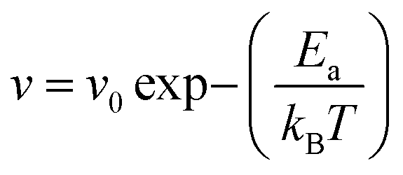
However, conventional DLTS has the major limitation of unreliable minority-carrier trap detection. In this regard, a novel optical-DLTS (O-DLTS) technique has emerged, which can effectively probe the majority and minority-carrier traps simultaneously. Deconvolution of DLTS spectra reveals distinctive (positive) peaks and (negative) valleys, which correspond to the majority and minority carrier traps, respectively. As a standard procedure, the defect activation energy (Ea) and capture cross-section (σ) are calculated using the Arrhenius plot line-fitting (APL) method. The Shockley–Read–Hall emission of carriers from the trap states is a thermal activation process. The emission rate (v) of carriers from the defect is essentially the Arrhenius equation, as follows:
 | (9) |
The distinctive Q-1D crystal structure and low structural symmetry in Sb2X3 induce unconventional and complicated defect physics. When defects are formed on non-equivalent sites (two non-equivalent Sb sites, i.e., Sb1 and Sb2, and three non-equivalent X sites, i.e., X1, X2, and X3), the formation energies and charge-state transition levels are different, resulting in multiple inherent defects.68,69 Unambiguously, the defect types are closely related to the growth conditions, in which VS/VSe (S/Se-vacancy) and SbS/SbSe (Sb-antisites) defects are formed under Sb-rich conditions, whereas VSb (Sb-vacancy) and SeSb/SSb (Se/S-antisites) are dominant under Se- or S-rich conditions.25,26 Interestingly, these defects are located at around the mid-gap with densities (NT) in the range of 1015–1017 cm−3, and τeff is measured to be in the range of 1.3–67 ns.70,71 Huang et al.68 performed an in-depth study on the defects in Sb2Se3via first principles calculations. Owing to presence of two non-equivalent Sb sites (Sb1 and Sb2), and three Se sites (Se1, Se2 and Se3), there are two Sb vacancies (VSb1 and VSb2), three Se vacancies (VSe1, VSe2 and VSe3), two SeSb antisites (SeSb1 and SeSb2), and three SbSe antisites (SbSe1, SbSe2 and SbSe3). The cation-replace-anion (SbSe) and anion-replace-cation (SeSb) antisite defects can have high concentrations and be dominant in Sb2Se3. Interestingly, two Se replacing one Sb (2SeSb) antisite defect can also have a high concentration under Se-rich conditions owing to the large space between different [Sb4Se6]n ribbons and produce a shallow acceptor level. Computational studies revealed that cation–anion antisite defects have low formation energies and are located near the middle of the bandgap, acting as recombination centers.6,29,72,73
Lian et al.74 conducted an O-DLTS study to probe the deep-level defects in Sb-rich and S-rich Sb2S3 films and solar cells. The results showed that the Sb-rich film displayed three donor defects (E1, E2 and E3, acting as electron traps), with the energy level of 0.31, 0.60, and 0.69 eV below the CBM, respectively (Fig. 2e). In contrast, the S-rich film exhibited only two acceptor defects (H1 and H2, acting as hole traps) with the energy levels of 0.64 and 0.71 eV above the VBM, respectively (Fig. 2h). The E1, E2, E3, H1, and H2 carrier traps were attributed to the Sb-interstitial (Sbi), S-vacancy (VS), SbS antisite, Sb-vacancy (VSb), and SSb antisite defects, respectively. The E2 (VS) and E3 (SbS) traps in the Sb-rich Sb2S3 films had a larger capture cross-section, higher trap density, and located closer to the Fermi energy level (EF) compared to H1(VSb) and H2 (SSb) in the S-rich Sb2S3. There is a high possibility that the electron quasi-EF is pinned near the E2 and E3 traps in Sb-rich Sb2S3. In contrast, S-rich Sb2S3 displayed a reduced capture cross section and defect density, resulting in suppressed recombination and prolonged carrier lifetimes. The trap state distribution is schematically shown in Fig. 2d–h and the parameters are listed in Table 1. The TAS decay profile (Fig. 2c) revealed that the S-rich Sb2S3 films exhibit much longer carrier lifetimes (18.7 ns) than the Sb-rich Sb2S3 films (3.8 ns). The reduced defect type (and density) contributed to the prolonged carrier lifetimes, improved VOC and PCE. The S-deficit in the Sb-rich Sb2S3 resulted in the inevitable formation of VS. Subsequently, the excess Sb preferentially filled the VS, rather than entering the interstitial site, given that the formation energy for SbS was lower than that for Sbi. Therefore, the E2 (VS) and E3 (SbS) defects were predominant in the Sb-rich Sb2S3. However, in the S-rich Sb2S3, initially, the S atoms entered the crystal structure to passivate VS. Under the S-rich conditions, the formation of SbS and Sbi defects was suppressed due to their increased formation energy, while the formation of a large amount of H1 (VSb) was induced due to its low formation energy. Furthermore, some S atoms may even occupy the VSb and form the H2 (SSb) antisite to maintain structural stability. It was also revealed that the Sbi defect did not have a critical influence on the carrier lifetimes, indicating the high tolerance of the Q-1D crystal structure. The space in (Sb4S6)n ribbons can easily accommodate impurities/defects to a certain extent. Cai et al.75 performed a first principles study on Sb2S3 and concluded that the formation energies of the dominant acceptor defects (VSb2, SbS2, and SSb2) and donor defect (VS2) in intrinsic Sb2S3 are similar. This results in EF level pinning near the middle of the band gap. These results are consistent with the experimentally observed high resistivity values (∼108 Ω cm) in undoped Sb2S3 thin films. It is widely accepted that the high resistivity in Sb2S3 originates from the compensation between its intrinsic donor (VS) and acceptors (VSb, SbS, and SSb), which have comparably high densities and low formation energies. This compensation also limits the improvement in conductivity through direct extrinsic doping.
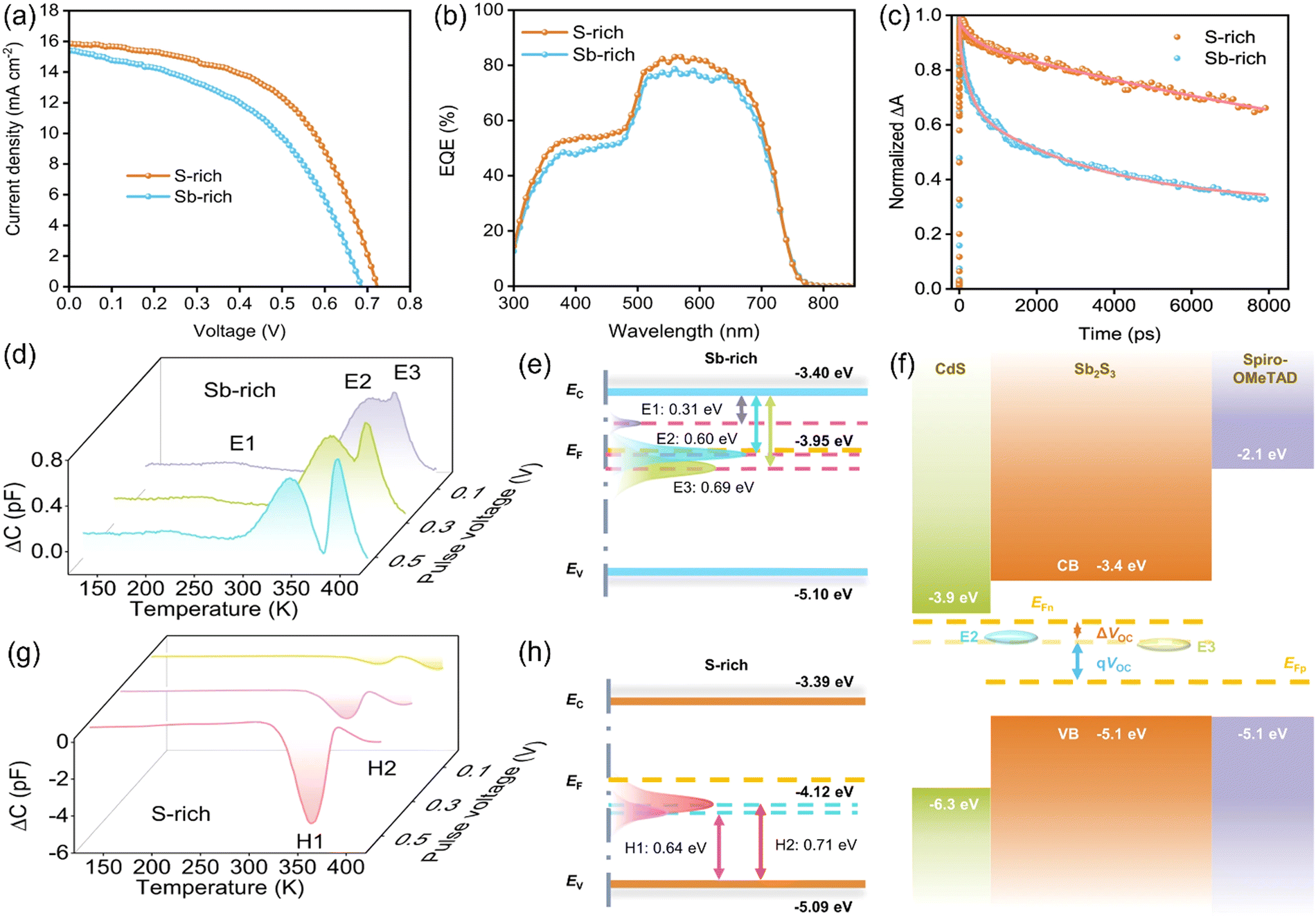 | ||
| Fig. 2 (a) J–V characteristics and (b) EQE spectra of the fabricated Sb2S3 solar cells. (c) Transient kinetic decay (scatter) and fittings according to biexponential decay function (solid lines) monitored at 545 nm of Sb-rich and S-rich films. (d) DLTS signals of Sb-rich and (g) S-rich Sb2S3 films at different pulse voltages ranging from 0.1 to 0.5 V, synergized with an identical pulse-width optical pulse. (d) Conduction band (EC), valence band (EV), Fermi level (EF), and trap energy level (ET) of Sb-rich and (h) S-rich Sb2S3 films. (f) Schematic diagram of VOC derived from splitting of the electron and hole quasi-Fermi levels. Adapted under the guidelines of the Creative Commons CC BY license from ref. 74 Copyright 2019, Nature Springer. | ||
| Material | Deposition technique | Defect characterization technique | Trap | Type | E T (eV) | σ (cm2) | N T (cm−3) | Ref. |
|---|---|---|---|---|---|---|---|---|
| Sb2S3 | Chemical bath deposition (CBD) | O-DLTS | H1 | SSb2 | E V + 0.500 | 1.24 × 10⁻¹⁷ | 1.85 × 10¹³ | 8 |
| H3 | SSb1 | E V + 0.776 | 6.59 × 10⁻¹⁶ | 1.57 × 10¹⁴ | ||||
| Hydrothermal | H1 | VSb | E c − 0.572 | 2.98 × 10⁻¹⁷ | 4.22 × 10¹³ | 82 | ||
| H2 | SbS2 | E c − 0.671 | 3.81 × 10⁻¹⁶ | 2.69 × 10¹⁴ | ||||
| H1 | VSb | E V + 0.576 | 2.52 × 10⁻¹⁷ | 6.67 × 10¹³ | 81 | |||
| H2 | SSb | E V + 0.701 | 4.37 × 10⁻¹⁶ | 1.08 × 10¹⁴ | ||||
| DLTS | H1 | VSb | E V + 0.536 | 2.39 × 10⁻¹⁶ | 3.71 × 10¹⁵ | 5 | ||
| H2 | SbS | E V + 0.709 | 4.49 × 10⁻¹⁴ | 3.67 × 10¹⁵ | ||||
| Thiourea-treated Sb2S3 | H1 | VSb | E V + 0.537 | 1.68 × 10⁻¹⁶ | 3.52 × 10¹⁵ | |||
| H2 | SbS | E V + 0.697 | 2.62 × 10⁻¹⁴ | 4.50 × 10¹⁴ | ||||
| E1 | Si | E C − 0.325 | 1.12 × 10⁻¹⁷ | 1.16 × 10¹⁴ | ||||
| Sb2S3 | H1 | SbS | E V + 0.445 | 6.14 × 10⁻¹⁵ | 2.16 × 10¹³ | 77 | ||
| H2 | E V + 0.698 | 2.31 × 10⁻¹⁶ | 4.25 × 10¹⁴ | |||||
| (NH4)2S-treated Sb2S3 | H2 | E V + 0.708 | 6.85 × 10⁻¹⁶ | 6.29 × 10¹³ | ||||
| Sb2S3 | E1 | VS | E C − 0.325 | 6.90 × 10⁻¹⁷ | 6.57 × 10¹⁴ | 83 | ||
| H1 | SbS | E V + 0.546 | 8.33 × 10⁻¹⁷ | 1.20 × 10¹⁵ | ||||
| H2 | E V + 0.673 | 1.14 × 10⁻¹⁶ | 2.26 × 10¹⁵ | |||||
| E1 | VS | E C − 0.255 | 6.39 × 10⁻¹⁸ | 1.02 × 10¹⁶ | 84 | |||
| H1 | VSb | E V + 0.321 | 2.15 × 10⁻¹⁶ | 1.15 × 10¹⁴ | ||||
| H2 | SbS2 | E V + 0.467 | 5.08 × 10⁻¹⁶ | 1.55 × 10¹⁴ | ||||
| H3 | SbS1 | E V + 0.579 | 7.15 × 10⁻¹⁷ | 3.14 × 10¹⁶ | ||||
| H4 | SbS3 | E V + 0.781 | 8.42 × 10⁻¹⁵ | 2.10 × 10¹⁶ | ||||
| O-DLTS | H1 | Sbs | E V + 0.664 | 4.05 × 10⁻¹⁶ | 1.26 × 10¹⁴ | 76 | ||
| H2 | E V + 0.713 | 4.47 × 10⁻¹⁵ | 1.19 × 10¹⁴ | |||||
| H3 | E V + 0.741 | 2.39 × 10⁻¹⁴ | 7.30 × 10¹³ | |||||
| H1 | SbS2 | E V + 0.507 | 1.27 × 10⁻¹⁵ | 1.46 × 10¹⁵ | 80 | |||
| H2 | SbS1 | E V + 0.689 | 4.95 × 10⁻¹⁷ | 3.42 × 10¹⁵ | ||||
| H3 | SbS3 | E V + 0.762 | 4.45 × 10⁻¹⁴ | 7.62 × 10¹⁵ | ||||
| Sb2(S,Se)3 | H1 | SbS2 | E V + 0.502 | 1.05 × 10⁻¹⁷ | 2.24 × 10¹⁴ | |||
| H3 | SbS3 | E V + 0.766 | 1.28 × 10⁻¹⁵ | 1.21 × 10¹⁵ | ||||
| DLTS O-DLTS | E1 | SbSe2 | E C − 0.57 | 2.48 × 10⁻¹² | 1.45 × 10¹⁵ | 85 | ||
| E2 | SbSe1 | E C − 0.71 | 4.39 × 10⁻¹² | 4.78 × 10¹⁵ | ||||
| H1 | SbS | E V + 0.761 | 3.97 × 10⁻¹⁵ | 6.45 × 10¹⁵ | ||||
| KI-treated Sb2(S,Se)3 | E1 | SbSe2 | E C − 0.584 | 1.99 × 10⁻¹³ | 6.49 × 10¹⁴ | |||
| H1 | SbS | E V + 0.784 | 1.6 × 10⁻¹⁴ | 2.97 × 10¹⁵ | ||||
| Sb2(S,Se)3 | H1 | SbS1 | E V + 0.500 | 1.99 × 10⁻¹⁷ | 6.28 × 10¹² | 10 | ||
| H2 | SbS2 | E V + 0.671 | 5.91 × 10⁻¹⁷ | 1.88 × 10¹³ | ||||
| E1 | VS2 | E c − 0.747 | 1.60 × 10⁻¹⁶ | 2.47 × 10¹³ | 49 | |||
| H1 | SeSb | E V + 0.290 | 6.61 × 10⁻¹⁷ | 6.55 × 10¹² | ||||
| H2 | SbS1 | E V + 0.638 | 3.18 × 10⁻¹⁵ | 4.15 × 10¹² | ||||
| H3 | SbS2 | E V + 0.483 | 1.48 × 10⁻¹⁶ | 4.64 × 10¹⁴ | ||||
| H4 | SbSe2 | E V + 0.682 | 3.67 × 10⁻¹⁴ | 8.63 × 10¹⁴ | ||||
| H5 | SbS3 | E V + 0.790 | 4.87 × 10⁻¹⁴ | 9.75 × 10¹⁴ | ||||
| DLTS | H1 | SbS | E V + 0.560 | 5.98 × 10⁻¹⁸ | 4.97 × 10¹⁵ | 86 | ||
| H2 | E V + 0.770 | 2.68 × 10⁻¹⁶ | 6.40 × 10¹⁵ | |||||
| E1 | SSb | E c − 0.563 | 1.40 × 10⁻¹⁶ | 1.97 × 10¹⁵ | ||||
| Admittance Spectroscopy | H1 | VSe | E V + 0.203 | 2.43 × 10⁻¹⁹ | 5.37 × 10¹⁴ | 87 | ||
| H2 | SbSe | E V + 0.364 | 3.85 × 10⁻¹⁶ | 1.27 × 10¹⁵ | ||||
| Sb2Se3 | CBD | O-DLTS | H1 | SeSb1 | E V + 0.609 | 3.23 × 10⁻¹⁷ | 1.01 × 10¹³ | 9 |
| H2 | SeSb2 | E V + 0.691 | 3.30 × 10⁻¹⁵ | 4.27 × 10¹² | ||||
| Vapor transport deposition (VTD) | Admittance spectroscopy | H1 | Bulk trap | E V + 0.286 | 3.2 × 10⁻¹⁷ | 2.46 × 10¹⁴ | 88 | |
| H2 | E V + 0.188 | 9.9 × 10⁻²¹ | 1.36 × 10¹⁵ | |||||
| H3 | Interface trap | E V + 0.570 | 4.1 × 10⁻¹⁶ | 1.15 × 10¹⁶ | ||||
| Rapid thermal evaporation (RTE) | Temperature-dependent (dark) conductivity and admittance spectroscopy | H1 | SeSb | E V + 0.111 | — | 1.3 × 10¹⁵ | 89 | |
| H2 | — | E V + 0.578 | — | — | ||||
| VTD | DLTS | H1 | VSb | E V + 0.48 | 1.5 × 10⁻¹⁷ | 1.2 × 10¹⁵ | 90 | |
| H2 | SeSb | E V + 0.71 | 4.9 × 10⁻¹³ | 1.1 × 10¹⁴ | ||||
| E1 | SbSe | E C − 0.61 | 4.0 × 10⁻¹³ | 2.6 × 10¹⁴ | ||||
| Injection vapor deposition (IVD) | E1 | VSe | E C − 0.206 | 5.34 × 10⁻²¹ | 2.74 × 10¹⁴ | 91 | ||
| E2 | SeSb2 | E C − 0.569 | 1.24 × 10⁻¹⁶ | 8.02 × 10¹⁴ | ||||
| H1 | SeSb2 | E V + 0.531 | 3.79 × 10⁻¹⁸ | 3.48 × 10¹⁴ | ||||
| Closed-space sublimation (CSS) | E1 | VSe2 | E C – 0.359 | 1.03 × 10⁻¹⁸ | 2.70 × 10¹⁴ | 15 | ||
| E2 | SbSb2 | E C – 0.609 | 1.54 × 10⁻¹⁶ | 1.73 × 10¹⁵ | ||||
| H1 | SeSb2 | E V + 0.691 | 1.37 × 10⁻¹⁶ | 8.76 × 10¹⁴ | ||||
| Spin coating | H1 | VSb | E V + 0.479 | 2.07 × 10⁻¹⁶ | 6.10 × 10¹⁴ | 92 | ||
| H2 | SeSb | E V + 0.713 | 1.53 × 10⁻¹⁴ | 1.00 × 10¹⁵ | ||||
| E1 | SbSe | E c − 0.628 | 7.05 × 10⁻¹⁷ | 6.49 × 10¹⁴ | ||||
| (2.21%) Te-doped Sb2Se3 | H1 | Vsb | E V + 478 | 2.71 × 10⁻¹⁵ | 5.34 × 10¹³ | |||
| E1 | SbSe | E c − 0.637 | 9.48 × 10⁻¹⁶ | 3.32 × 10¹⁴ | ||||
| (5.23%) S-doped Sb2Se3 | H1 | VSb | E V + 0.500 | 6.80 × 10⁻¹⁴ | 6.93 × 10¹⁴ | |||
| H2 | SeSb | E V + 0.721 | 8.19 × 10⁻¹⁴ | 1.43 × 10¹⁵ | ||||
| E1 | SbSe | E c − 0.633 | 2.54 × 10⁻¹⁶ | 6.60 × 10¹⁴ |
Wang et al.8 fabricated Sb2S3 solar cells via chemical bath deposition (CBD) employing six different routes. It was demonstrated that using multiple S-sources (sodium thiosulfate and thioacetamide) accelerated the release of S2− ions, leading to the formation of S-rich Sb2S3 films with better morphology (average grain size ∼2.8 μm), crystallographic orientation, prolonged carrier lifetimes and less defects. Energy dispersive X-ray (EDX) analysis revealed atomic ratios of S/Sb of >1.5 for all the Sb2S3 films, indicating the (desirable) S-richness in the films. The defects in the n-Sb2S3 films were characterized via O-DLTS. The O-DLTS signal revealed only negative peaks, suggesting the presence of minority traps (holes), i.e., H1, H2 and H3, with Ea of ≈0.51, 0.66, and 0.77 eV, respectively (Fig. 3). H1 and H3 were attributed to the antisite defects (SSb2 and SSb1, respectively), while H2 to VSb2. All three traps were found to be located below the intrinsic EF. Compared to the H2 and H3 traps, the H1 trap was located further away from EF, which was generally submerged in electrons and remained passive. The H1 trap exhibited a lower trap density and smaller capture cross-section, and thus a less detrimental effect on carrier trapping. On the contrary, the deep-level H3 (SSb1) trap was located closer to EF and exhibited a larger capture cross-section than the other traps, and thus was the most active in charge trapping. The devices fabricated using the modified recipe were free from the H2 deep-level defect (VSb2) and demonstrated a record PCE of 8.0% in Sb2S3 solar cells. Furthermore, bi-exponential fitting of the TAS curve revealed a prolonged carrier lifetime of 9298 ps in the FTO/CdS/Sb2S3 stack, indicating efficient transport and reduced recombination. Furthermore, an excellent diode ideality factor of 1.31 and low reverse saturation current were obtained, suggesting the substantial suppression of non-radiative (SRH) recombination in the device.
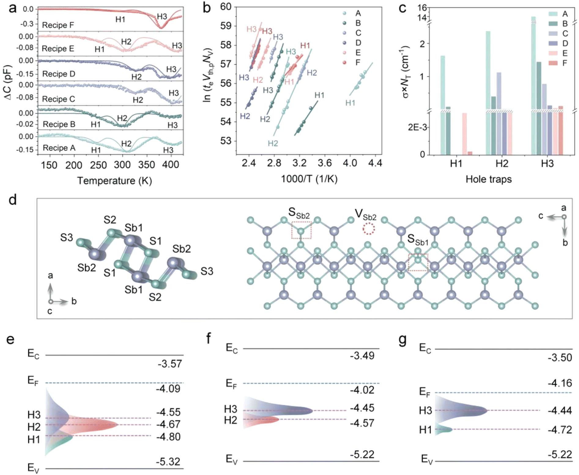 | ||
| Fig. 3 (a) O-DLTS signals and high-resolution evaluation simulations for Sb2S3 solar cells based on recipes A–F. (b) Corresponding Arrhenius plots obtained from the O-DLTS signals. (c) Histogram of the calculated σ × NT values of different hole traps in Sb2S3 solar cells based on recipes A–F. (d) Schematic diagram of an Sb4S6 ribbon with five nonequivalent atomic sites and SSb1, SSb2, and VSb2 defects in the Sb2S3 lattice. (e)–(g) Energy levels and defect levels of the devices based on recipes B, D, and F, respectively. Adapted with permission from ref. 8 Copyright 2022, Wiley-VCH. | ||
Huang et al.76 demonstrated in situ sulfurization by introducing tartaric acid (TTA) additive in the hydrothermal deposition process of Sb2S3. The consensus is that reducing the density of SbS defect is one key aspect to enhance the PCE of Sb2S3 solar cells. S atoms easily volatilized from the Sb2S3 thin films during annealing to form VS. Given that the formation energy of Sbi is much higher than that of SbS, excess Sb preferentially filled the VS voids, thus forming SbS antisite defects. In situ sulfurization induced S-richness in the annealed Sb2S3 films. Consequently, this increased the formation energy of SbS defects. To accommodate the stability of the structure in S-rich Sb2S3 films, some of the S atoms occupied VSb to form SSb defects. In situ sulfurization successfully compensated the S-loss occurring during annealing and suppressed the formation of SbS. Three hole traps (H1, H2 and H3) were obtained for the control Sb2S3 sample, which are attributed to SbS defects. In the case of the sulfurized sample, only H1 and H3 traps were obtained. The passivation of the SbS defects and improvement in crystallinity led to an improved PCE (6.31%) in the in situ-sulfurized device, outperforming the control device (PCE of 5.46%).
Huang et al.77 demonstrated a novel (NH4)2S-induced hydrothermal sulfurization process for the fabrication of Sb2S3 solar cells. (NH4)2S undergoes hydrolysis to produce H2S, a strong sulfurization agent. The XRD patterns revealed improvements in crystallinity, while the SEM micrographs suggested no improvement in morphology on adopting the sulfurization strategy. DLTS analysis revealed the presence of two minority carrier (hole) traps, i.e., H1 and H2, in the control films, with the activation energy of 445 and 698 meV, respectively, which were both attributed to SbS antisite defects. The sulfurization process annihilated H1, given that only H2 was detected in the sulfurized films. The PCE of the solar cell (FTO/CdS/Sb2S3/spiro-OMeTAD/Au) improved from 6.01% to 6.92% on adopting the sulfurization strategy. The reverse (leakage) current density (Jo) value decreased from 4.85 × 10⁻² mA cm−2 to 2.07 × 10⁻⁵ mA cm−2 in the respective devices, indicating a significant improvement in diode quality and rectification characteristics. Choi et al.78 investigated the trap-state distribution in CBD-deposited and post-deposition thioacetamide (TA, CH3CSNH2)-treated Sb2S3 films using capacitance transient-based DLTS, where Sb2S3/Au-based Schottky diodes (500 mm diameter) were fabricated for the measurement. TA decomposed into volatile acetonitrile (CH3CN) and hydrogen sulfide (H2S) gas on annealing at temperatures exceeding 150 °C in an inert atmosphere. The released H2S readily reacted with the surface of the Sb2S3 film, passivating the VS defects and reducing the oxide phase (oxidized sulfur, sulfates, and Sb2O3). Interestingly, the untreated sample demonstrated a single hole trap with an activation energy of Ev +0.52 eV, capture cross-section of 1.34 × 10⁻¹⁷ cm2 and density of (2–5) ×1014 cm−3, while no trap was found for the TA-treated sample. TA treatment was found to be instrumental in boosting the VOC and PCE values from 570.5 meV and 5.5% (in the control device) to 645.7 meV and 7.5% (in champion device), respectively. This spectacular improvement was attributed to the annihilation of Vs defects (near the Sb2S3/HTL) by H2S-assisted sulfurization. H2S-assisted sulfurization has also been found to be instrumental in passivating VS/Se defects, reducing the (detrimental) Sb2O3 phase (at the surface) and boosting the carrier lifetimes and mobility in Sb2Se3 films.79
Similar to TA, thiourea (TU, SC(NH2)2) treatment has also been used as an effective sulfurization strategy (by releasing H2S during decomposition at temperatures of >150 °C) for passivating VS/Se defects in Sb2X3 films. Qi et al.5 performed an investigation on the trap physics in hydrothermally deposited Sb2S3 films using DLTS. The as-deposited films exhibited two minority (hole) traps, i.e., H1 and H2 (attributed to VSb and SbS, respectively). These defects possessed high ionization energies of 0.536 and 0.709 eV, respectively, and served as severe recombination centers. H2 was highly effective in charge trapping and VOC loss (owing to its high density and large capture cross-section), while H1 was less effective (low capture cross section of ∼10−16 cm2). TU treatment on Sb2S3 films led to the suppression of the H2 (SbS) defect density by one order, suggesting the alleviation of S-deficiency at the surface.
Liang et al.15 fabricated flexible Sb2Se3 solar cells (Mo/Sb2Se3/CdS/ZnO/Al:ZO/Ag) on a polyimide (PI) substrate and investigated the influence of an ultra-thin PbSe layer (at the Mo/Sb2Se3 interface) on the device performance. The control device (without a PbSe interlayer), i.e., C–Sb2Se3, was found to underperform (PCE of 3.04%) compared to the device with a PbSe interlayer, i.e., Pb–Sb2Se3 (PCE of 8.43%). The improved performance of the latter was attributed to the synergistic influence of the PbSe layer in suppressing the unfavorable [hk0]-orientated grains, alleviating the Schottky barrier height (at the Mo/Sb2Se3 interface) and mitigating the bulk-defects in the absorber layer. The TPV study revealed longer carrier lifetimes (∼0.78 ms) in the Pb–Sb2Se3 devices in comparison to the C–Sb2Se3 devices (∼0.02 ms). The defect dynamics in both devices were investigated using DLTS (Fig. 4c–f). The Arrhenius plots (Fig. 4d) were found to be straight lines, suggesting that the activation energy Ea (slope of the plots) and capture cross-sections (calculated from the Y-intercept) were strictly independent of temperature. Two electron traps (E1 and E2) and one hole trap (H2) were identified from the DLTS signal in both devices (Fig. 4c). Trap E1 was attributed to the VSe2 vacancy defect. VSe exhibited a low formation energy under both Se-rich and Se-poor conditions and acted as shallow-level electron traps. Also, VSe exhibited a lower density and capture cross-section (listed in Table 1), and thus ruled out as a stringent recombination center. E2 and H1 were found to be located close and deeper in the forbidden gap, resulting in ambiguous interpretations. These traps could be either attributed to the donor–acceptor pair of the same (amphoteric) defect (SbSe) or [SbSe + SeSb] antisite complexes. The E2 and H1 defects in the Pb–Sb2Se3 solar cells were attributed to VSe3 and PbSb, respectively. H1 was found to be located much shallower and with (one order) lower capture cross-section in Pb–Sb2Se3 than in C–Sb2Se3, suggesting its impact in alleviating the carrier lifetimes, and the VOC was limited in the Pb–Sb2Se3 device.
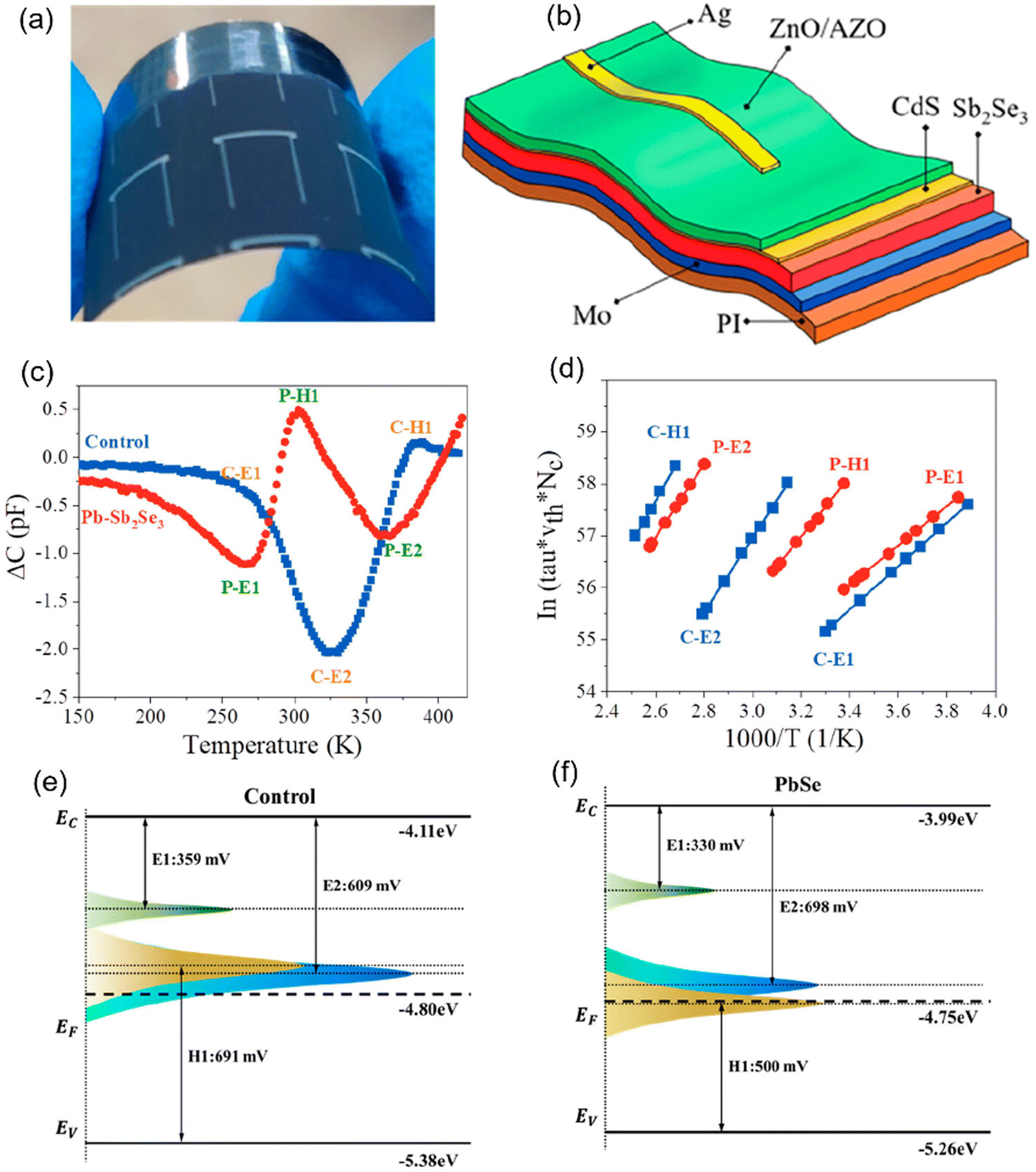 | ||
| Fig. 4 (a) Photograph and (b) schematic device structure of flexible Sb2Se3 solar cells fabricated on PI in a substrate configuration of PI/Mo/Sb2Se3(Pb–Sb2Se3)/CdS/ZnO/AZO/Ag. (c) DLTS signals of Pb–Sb2Se3 and the control devices. (d) Arrhenius plots obtained from DLTS signals. (e) and (f) Energy states and defect levels of the control device and Pb–Sb2Se3 solar cells. Adapted with permission from ref. 15 Copyright 2023, the American Chemical Society. | ||
Che et al.49 investigated the influence of the annealing process on the defect formation mechanism in hydrothermally deposited n-type Sb2(S,Se)3 films. High-temperature annealing (200–425 °C) led to a two-step defect transformation process, i.e., the formation of VSe/VS vacancy defects (with high formation energies), followed by the migration of Sb ions to fill the vacancy defects (forming antisite defects with low formation energies). O-DLTS analysis revealed the presence of one electron trap (E1) and five-hole traps (H1, H2, H3, H4, and H5) in the samples. The former was assigned to S-vacancy (VS2), while the latter to antisite defects (SeSb, SbS1, SbS2, SbSe2, and SbS3, respectively). H2–H5 acted as amphoteric defects. E1 (VS2), H1 (SeSb) and H2 (SbS1) defects with high formation energies appeared in the as-deposited (unannealed) film (Fig. 5c). After post-annealing, these traps gradually decreased and transformed into H3–H5 antisite defects (i.e., SbS2, SbSe2, and SbS3), respectively, with lower formation energies. It was concluded that post-annealing provided a driving force for the formation of relatively low-energy defects. S-volatilization left sulfur vacancies (E1, VS), which were subsequently occupied by the Sb atoms, as depicted by the P3 process (Fig. 5e), thus creating Sb-substituted S (H3, SbS2) anti-site defect. Furthermore, owing to the instability (high formation energy) of the SeSb (H1) defect, the Se atoms (in SeSb) migrate to occupy neighboring VS(e) under the thermal driving force, leading to the mitigation of H1, as shown by the P1 process. Se-volatilization forms VSe, which gets occupied by the neighboring Sb atoms, forming Sb-antisite defect (H4, SbSe2), as shown by the P4 process (Fig. 5e). Concurrently, the further loss of S (during annealing) creates more VS, which prompts the Sb atoms to occupy these unstable VS3 (P5 process in Fig. 5e), leading to the creation of a new low-formation energy defect, i.e., SbS3 (H5). Interestingly, the elevated annealing temperature propelled the Sb atoms in the high-formation energy defect H2 (SbS1) to migrate to the surrounding VS(e) and form defects SbS(e) (depicted by the P2 process). VS2, SbS1, SbSe2, and SbS3 are all located near the EF-level, which significantly influenced the carrier lifetimes and VOC. The transient absorption spectroscopy (TAS) results revealed that the Sb2(S,Se)3 film annealed at 350 °C for 10 min exhibited the longest carrier lifetime (7.0 ns) compared to the films annealed at other temperatures and for higher durations. It was concluded that the Sb2(S,Se)3 films annealed at 350 °C exhibited the lowest defect concentrations and longest carrier lifetimes, thus leading to a high photovoltaic performance (PCE of 9.7%).
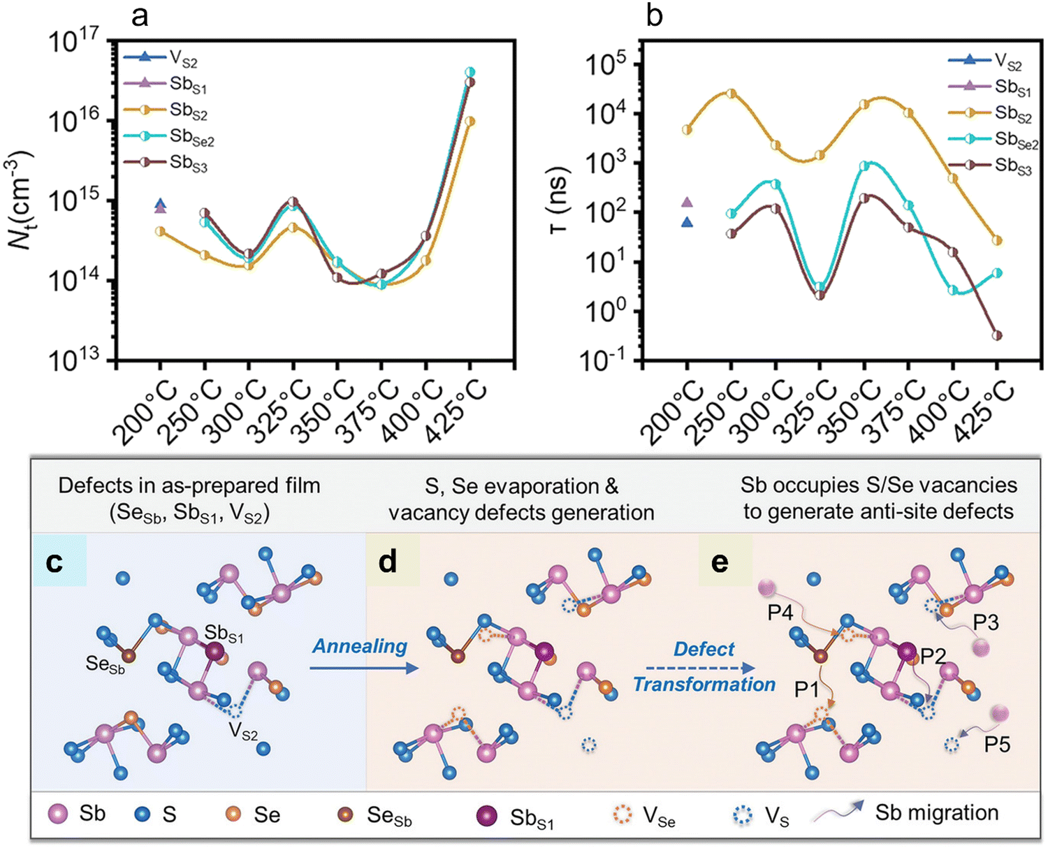 | ||
| Fig. 5 (a) Dependence of defect density (NT) on annealing temperature and (b) lifetime associated with specific defects obtained from the O-DLTS signals of the devices. Schematic of (c) three types of point defects in the as-deposited films (without post-annealing). (d) Loss of S and Se atoms to generate vacancy defects during annealing and (e) formation mechanism of antisite defects in the Sb2(S,Se)3 films. Adapted with permission from ref. 49 Copyright 2022, Wiley-VCH. | ||
Tang et al.80 investigated the defect properties in hydrothermally deposited Sb2S3 and Sb2(S,Se)3 films using O-DLTS. Three-hole traps (H1, H2 and H3) were detected in all the samples. Also, similar Ea values were obtained for the traps in all the samples, suggesting similar origins for each type of defect. Specifically, H1, H2 and H3 were located at about 0.50 eV, 0.68 eV and 0.76 eV above the valence band and assigned to antisite defects (SbS2, SbS1, and SbS3), respectively. Notably, the capture cross section exhibited a decreasing trend (up to two orders) with an increase in the Se-content in the films. Also, the H2 defect disappeared in the films with a higher Se-content, indicating that the defect properties are strongly correlated with the elemental composition and stoichiometry. An increase in Se-content not only induced preferred [hk1]-oriented growth, but also favored efficient carrier transport by alleviating the defect density and capture cross-section, leading to a PCE of 10.10% in the device employing the Sb2(S,Se)3 thin-film (with 29% Se-content), outperforming the Sb2S3-based device (PCE of 6.02%).
Zhao et al.9 conducted O-DLTS measurements in Se-rich Sb2Se3 films, which were synthesized using the CBD technique. Antimony potassium tartrate (APT) and sodium selenosulfate (SSS) were used as the Sb and Se sources, respectively, while thiourea (TU) and selenourea (SU) were used as additives. The films were synthesized via three routes, i.e., APT + SSS (no additive), APT + SSS +TU (additive) and APT + SSS + SU (additive). The additives were found to be instrumental in regulating the reaction kinetics and defect properties of the Sb2Se3 films (Fig. 6d). The detailed defect parameters extracted from the Arrhenius curves (Fig. 6e) and DLTS signals are summarized in Table 1. Two types of hole traps (H1 and H2) were detected in all the samples, which are attributed to Se-antisites (SeSb1 and SeSb2, respectively). Under Se-rich conditions, the SeSb1 and SeSb2 antisite defects have relatively low formation energies (<1 eV), making the replacement of Sb with Se feasible. The Se-antisite defects form deep-level defects, inducing EF-level pinning and serving as proactive SRH-recombination centers. Furthermore, the Se-antisite defects are specifically amphoteric defects with similar carrier capture cross-sections for both electrons and holes, thus severely impeding the carrier transport and limiting the final PV performance. The H2 trap level is located deeper in the band gap than H1, implying that H2 is the dominant defect in these films. The control Sb2Se3 device had a higher trap density (6.65 × 1013 cm−3) of H2, which is consistent with its poor film quality. After regulating the CBD reaction in the deposition processes, the values of NT significantly decreased. Particularly, the H2 defect density of the SU-Sb2Se3 device was reduced by one order of magnitude, alleviating the SRH recombination. The mitigation of the non-radiative recombination pathways is consistent with the J–V measurements in the dark and at different light intensities. It was concluded that the sensitive manipulation of the reaction kinetics via the additive-assisted CBD technique offers an effective route for the fabrication of high-quality Sb2Se3 films and high-PCE (10.57%) solar cells.
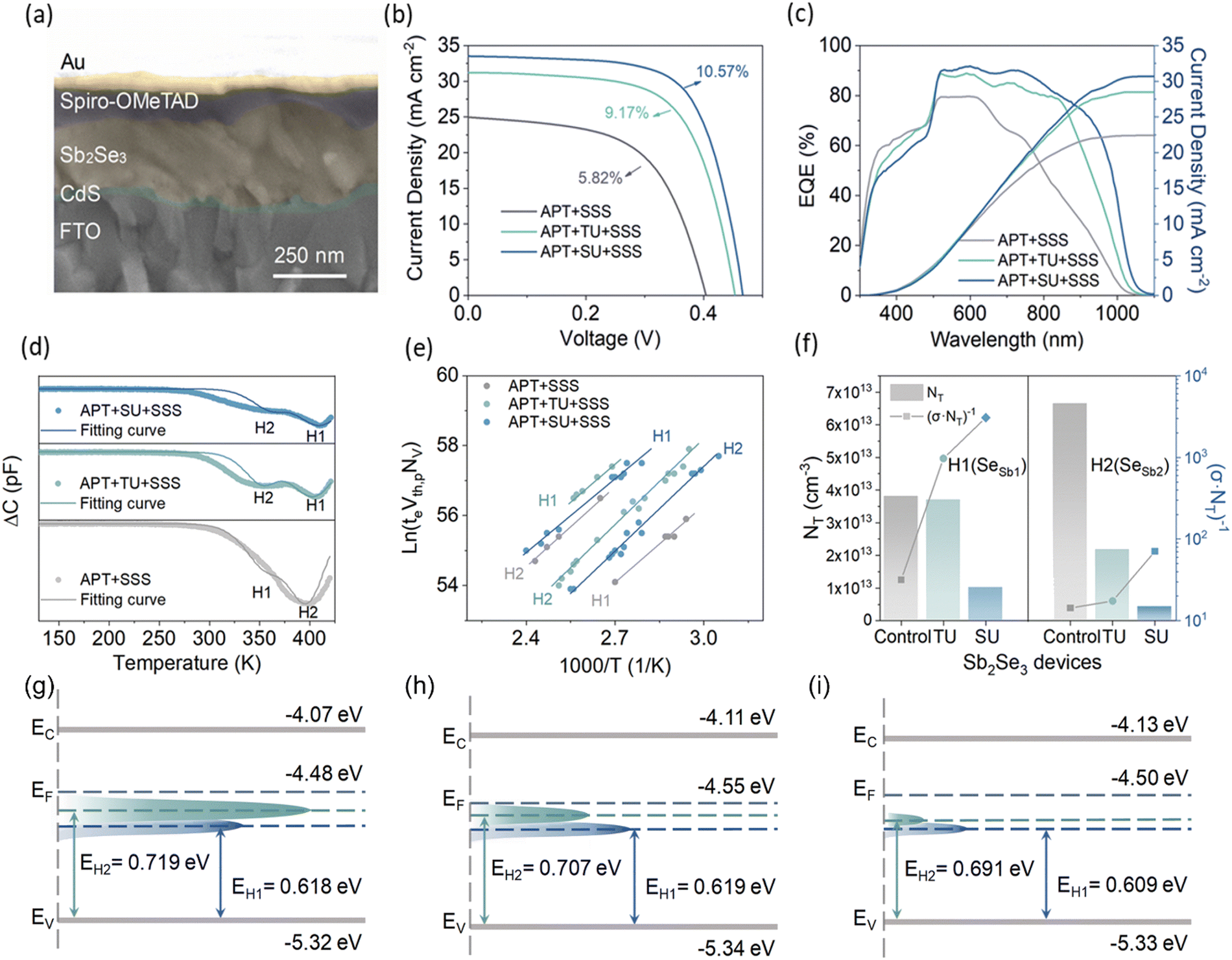 | ||
| Fig. 6 (a) Cross-sectional SEM image of Sb2Se3 planar heterojunction solar cell. (b) J–V curves and (c) EQE spectra of the Sb2Se3 solar cells fabricated via three different routes. Plots (d)–(i) show the deep-level defect profile in the Sb2Se3 films. (d) O-DLTS signals from Sb2Se3 devices. (e) Arrhenius plots obtained from O-DLTS signals. (f) Values of NT (left) and (σ·NT)−1 (right) for all the Sb2Se3 samples at the H1 (SeSb1) and H2 (SeSb2) defects. Deep-level defect profile of (g) control-Sb2Se3 film, (h) TU-Sb2Se3 film and (i) SU-Sb2Se3 film. Adapted with permission from ref. 9 Copyright 2022, The Royal Society of Chemistry Publishing. | ||
Wu et al.81 investigated the structure–property–performance relationship in Sb2S3 thin-film solar cells via the in-depth characterization of the crystal orientation, carrier transport and device performance. The study revealed that by merely controlling the post-annealing process, the grain growth, orientation and defect physics can be regulated. Normal grain growth occurred when the Sb2S3 film was subjected to a low-temperature treatment process, yielding [hk1]-oriented films. Alternatively, direct annealing at high temperature promoted abnormal grain growth and favored [hk0]-oriented Sb2S3 film growth. The device using the [hk1]-oriented Sb2S3 thin-film demonstrated a PCE of 6.82%, outperforming the devices based on an [hk0]-oriented absorber (6.27%). The O-DLTS results suggested that the [hk1]-oriented Sb2S3 film (with normal grain growth) exhibited only one type of hole trap (SSb), while the [hk0]-oriented film (with abnormal grain growth) demonstrated two types of hole traps (SSb and VSb). The dark J–V measurements revealed a higher leakage current in the latter device. Furthermore, the TAS analysis suggested a shorter average lifetime (tavg of ∼3924 ps) in the device with [hk1]-oriented Sb2S3 films than that with the [hk0]-oriented films (tavg of ∼4818 ps). The shorter lifetime and better performance were attributed to the rapid electron extraction by the ETL (CdS) layer and lower density of deep traps in the devices with the [hk1]-oriented Sb2S3 films than their [hk0] counterparts.
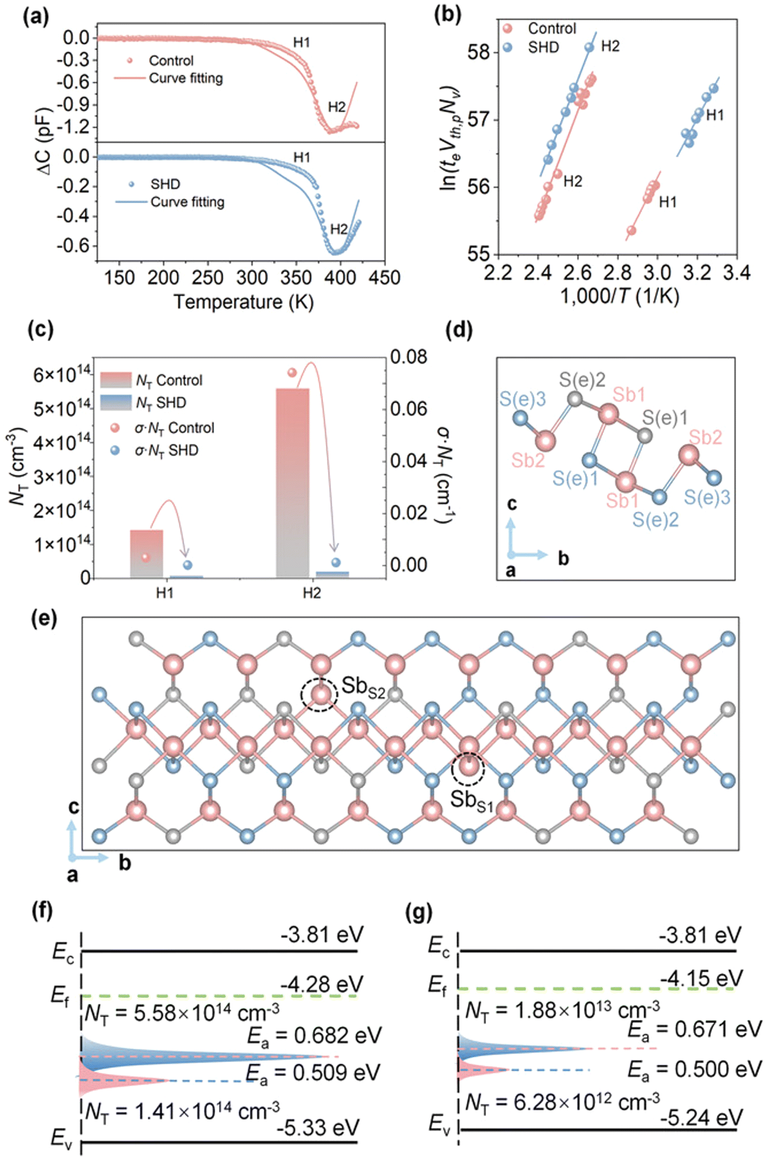
Chen et al.10 demonstrated a solvent-assisted hydrothermal deposition (SHD) technique for the deposition of high-quality Sb2(S,Se)3 films. Ethanol was used as an additive and found to be instrumental in regulating the reaction kinetics during the deposition procedure and stoichiometry in Sb2(S,Se)3 films. The devices fabricated using the ethanol-SHD technique demonstrated a substantial reduction in trap density and dark current density and higher recombination resistance (Rrec) than the control devices (Fig. 7c). The FTO/Sb2(S,Se)3/Au structure was adopted to measure the conductivity of the Sb2(S,Se)3 films, revealing an improvement in conductivity from 1.65 × 10⁻⁴ S cm−1 to 4.07 × 10⁻⁴ S cm−1 on adopting the novel route. The deep level defects in the films were probed using O-DLTS. Two-hole traps (H1 and H2) were obtained in the control films, which were attributed to SbS2 and SbS1 defects, respectively (Fig. 7a). The films synthesized using the SHD protocol exhibited one order of suppression in trap density of H1 and H2 defects, greatly benefiting the carrier transport. Consequently, the fabricated device (FTO/CdS/Sb2(S,Se)3/spiro-OMeTAD/Au) delivered a PCE of 10.75%, a record for Sb2X3 solar cells.
 | ||
| Fig. 7 Deep-level defect analysis. (a) O-DLTS signals and high-resolution evaluation simulations for Sb2(S,Se)3 solar cells without and with ethanol additive and (b) corresponding Arrhenius plots. (c) Values of NT and (σ·NT) at the H1 (SbS2) and H2 (SbS1) defects. (d) Schematic diagram of an Sb4S6 ribbon with five non-equivalent atomic sites. (e) SbS2 and SbS1 defects in Sb2(S,Se)3 lattice. Energy states and defect levels of the devices (f) without and (g) with ethanol. Adapted with permission from ref. 10 Copyright 2023, Wiley-VCH. | ||
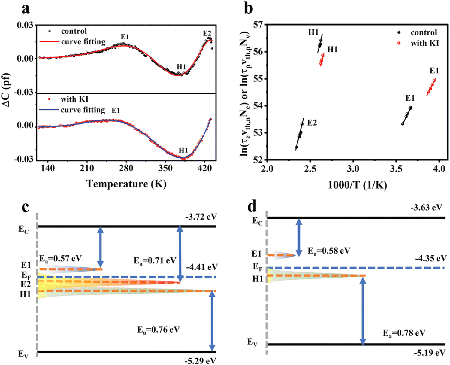
Li et al.85 investigated the role of potassium iodide (KI) surface treatment on Sb2(S,Se)3 thin films and solar cells. KI treatment was found to successfully improve the crystallinity and morphology of the Sb2(S,Se)3 films, inhibit the deep-level defects and improve the band alignment for efficient charge transport. It was revealed that I diffused into the Sb2(S,Se)3 crystal and induced the benign [211]-crystal orientation. The as-deposited films were Sb-rich, with SbS and SbSe antisites as the two dominant defects. The diffused I interacted strongly with the Sb atoms, forming Sb–I bonding. Therefore, I passivated the VS/Se defects, and thus inhibited the formation of the detrimental SbS and SbSe antisite defects. Fig. 8(a) illustrates the DLTS signal from the control and KI-treated device. Two majority (electron) traps and one minority (hole) trap were identified for the control device, which were denoted as E1 (SbSe2) and E2 (SbSe1) and H1 (SbS), respectively. KI treatment suppressed the density of E1 and H1, while annihilating the E2 defect (defect parameters summarized in Table 1). Furthermore, the KI-treated device exhibited a lower dark (reverse) current density and higher PCE (9.22%) than its untreated counterpart (PCE of 8.19%).
 | ||
| Fig. 8 (a) DLTS signals for the device without and with KI post-treatment. (b) Corresponding Arrhenius plots obtained from the DLTS signals. Position distribution of CBM (Ec), VBM (Ev), Fermi level (EF) and defect energy level for Sb2(S,Se)3 films (c) without and (d) with KI post-treatment. Adapted with permission from ref. 85 Copyright 2022, Wiley-VCH. | ||
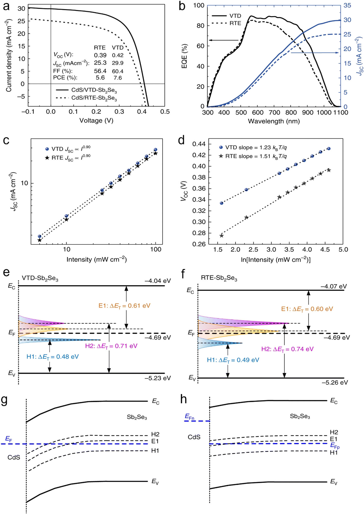
Wen et al.90 demonstrated a vapor transport deposition (VTD) technique to deposit Sb2Se3 thin films with improved film crystallinity, lengthier carrier lifetimes, and reduced bulk and interfacial defects. The champion device (ITO/CdS/Sb2Se3/Au) demonstrated a PCE of 7.6%, outperforming the device fabricated via RTE (PCE of 5.6%). As envisaged in Fig. 9(c), the power value (α) for both the devices was ∼0.9, i.e., closer to unity (first-order), suggesting that trap-assisted SRH recombination is the dominant loss mechanism. The diode ideality factor (η) decreased from 1.51 (for RTE-fabricated device) to 1.23 (for VTD-fabricated device), suggesting the mitigation of SRH recombination on switching the film deposition route (Fig. 9d). The CdS/Sb2Se3 interfacial defect density was quantitatively characterized via the capacitance–voltage (C–V) profiling and deep-level capacitance profiling (DLCP) techniques. The interfacial defect density of the RTE-fabricated and VTD-fabricated devices was calculated to be 2.1 × 1011cm−2 and 2.8 × 1010cm−2, respectively. Interestingly, during VTD deposition, Cd diffusion into the Sb2Se3 film transformed p-type Sb2Se3 into n-type, forming a buried homojunction at the CdS/Sb2Se3 interface. This led to suppressed interfacial defects, benefitting the device performance. The DLTS study revealed one electron trap (E1) and two hole traps (H1 and H2) in the Sb2Se3 films. The E1, H1 and H2 defects were attributed to the SbSe, VSb and SeSb defects, respectively. The VTD deposition process suppressed the density of the [SbSe + SeSb] antisite defect pair by more than an order of magnitude. As envisaged in Fig. 9(h), the H1 state was under EF and submerged in electrons, and thus the H1 defects always remained inert. In contrast, the H2 and E1 traps were above the EF and active in trapping holes and electrons, respectively. Moreover, owing to the higher defect density of H2 and E1 than the carrier concentration (∼1013cm−3) in the Sb2Se3 layer, the (hole) quasi EF-level (EFp) would be more likely to be pinned near the E1 and H2 levels.
 | ||
| Fig. 9 (a) J–V characteristics and (b) EQE plots of the VTD- and RTE-fabricated Sb2Se3 solar cells. Light intensity-dependent (c) JSC and (d) VOC of the devices. Energy states and defect level of (e) VTD-fabricated and (f) RTE-fabricated devices. Energy band diagrams at CdS/Sb2Se3 interface (g) in the dark and (h) under illumination. Reproduced under the guidelines of the Creative Commons CC-BY license from ref. 90 Copyright 2018, Springer Nature. | ||
Ma et al.92 investigated the influence of (0–4%) Te and S doping on Sb2Se3 films and investigated their deep-defect profiles using DLTS. It was revealed that the incorporation of Te was decisive in regulating the atomic ratio of Se/Sb, given that a sustained decline in Se content was observed with an increase in Te doping. Different crystal structures of Sb2Se3 and Sb2Te3 inhibited the formation of the alloy-Sb2(Se,Te)3 film, and therefore instead of going into the lattice, Te settled at the grain boundaries and surface. Se-rich Sb2Se3 favored the formation of SeSb and VSb defects, while the Sb-rich films benefited the formation of SbSe and VSe defects. The undoped Sb2Se3 demonstrated two-hole traps (H1 and H2) and one-electron trap (E1), acting as acceptor and donor defects, respectively. These defects were attributed to the antimony vacancy (VSb), selenium antisite (SeSb) and antimony antisite (SbSe) defects, respectively. Te-doping suppressed the hole-trap densities by eliminating the SeSb defects (H2) and mitigating the VSb defects (H1). However, for a high Te doping (∼4%), SbSe (E1) exhibited an order of increment in magnitude, and a new electron trap (E2, VSe) also started to appear in the DLTS signal. Interestingly, S-doping was found to have detrimental effects on the Sb2Se3 film and solar cell performance, given that S-incorporation could not emulate Te in suppressing the defect-formation process.
Duan et al.91 demonstrated a novel injection vapor deposition (IVD) technique for the deposition of high crystallinity, [001]-oriented Sb2Se3 films, with a minimal deep-level defect density. The Sb2Se3-based devices fabricated via IVD demonstrated a lower trap density, suppressed recombination losses and better performance (PCE of 10.12%) than the devices fabricated via close-spaced sublimation (CSS) and co-evaporation (CoE) method (PCE of 9.31% and 3.96%, respectively). Capacitance–voltage (C–V) profiling, deep-level capacitance profiling (DLCP) measurements, and minority carrier injection DLTS measurements were carried out to probe the interface and deep traps in the Sb2Se3 solar cells. Subsequently, bulk trap density (NT) values of 2.3 × 10¹⁶, 1.5 × 10¹⁶, and 5 × 1016 cm−3 were obtained for the devices with IVD-Sb2Se3, CSS-Sb2Se3 and CoE-Sb2S3 films, respectively. The corresponding devices exhibited an interface defect density of 1.32 × 10¹², 9.30 × 10¹² and 1.20 × 1012 cm−2, respectively. Furthermore, the DLTS analysis revealed one (type) electron trap (E1), two electron traps (E1 and E2), and two electron traps and one hole trap (E1, E2, and H1) in the CSS-Sb2Se3, IVD-Sb2Se3, and CoE-Sb2Se3 films (Fig. 10a–c), respectively. The IVD-E2, CSS-E1, and CoE-E2 defects were attributed to SeSb2, while CoE-H1 to the SeSb1 antisite traps. The capture cross section for the IVD-E1 trap was only ∼10−21 cm2, which was more than two orders of magnitude smaller than that for the other traps. It also exhibited a lower trap density of 2.74 × 1014 cm−3, thus having a less detrimental effect on the charge transport and device parameters. Interestingly, it was observed that during the CSS deposition of the Sb2Se3 absorber layers, the actual temperature of the substrate reached as high as 370–380 °C. The contribution of source radiative heating to the surface thermal energy became significant and [001]-oriented Sb2Se3 nanorods could be obtained in tens of seconds owing to the strong anisotropy in chemical-bonding. In contrast to CSS, the surface thermal energy in IVD is mainly attributed to the heating of the substrate. According to the terrace-ledge-kink (TLK) growth model, an increase in the growth temperature and surface thermal energy increases the critical radius for crystal growth and mitigates the density of stable nuclei, resulting in the formation of compact, [001]-oriented Sb2Se3 films with reduced donor–acceptor defect complexes.
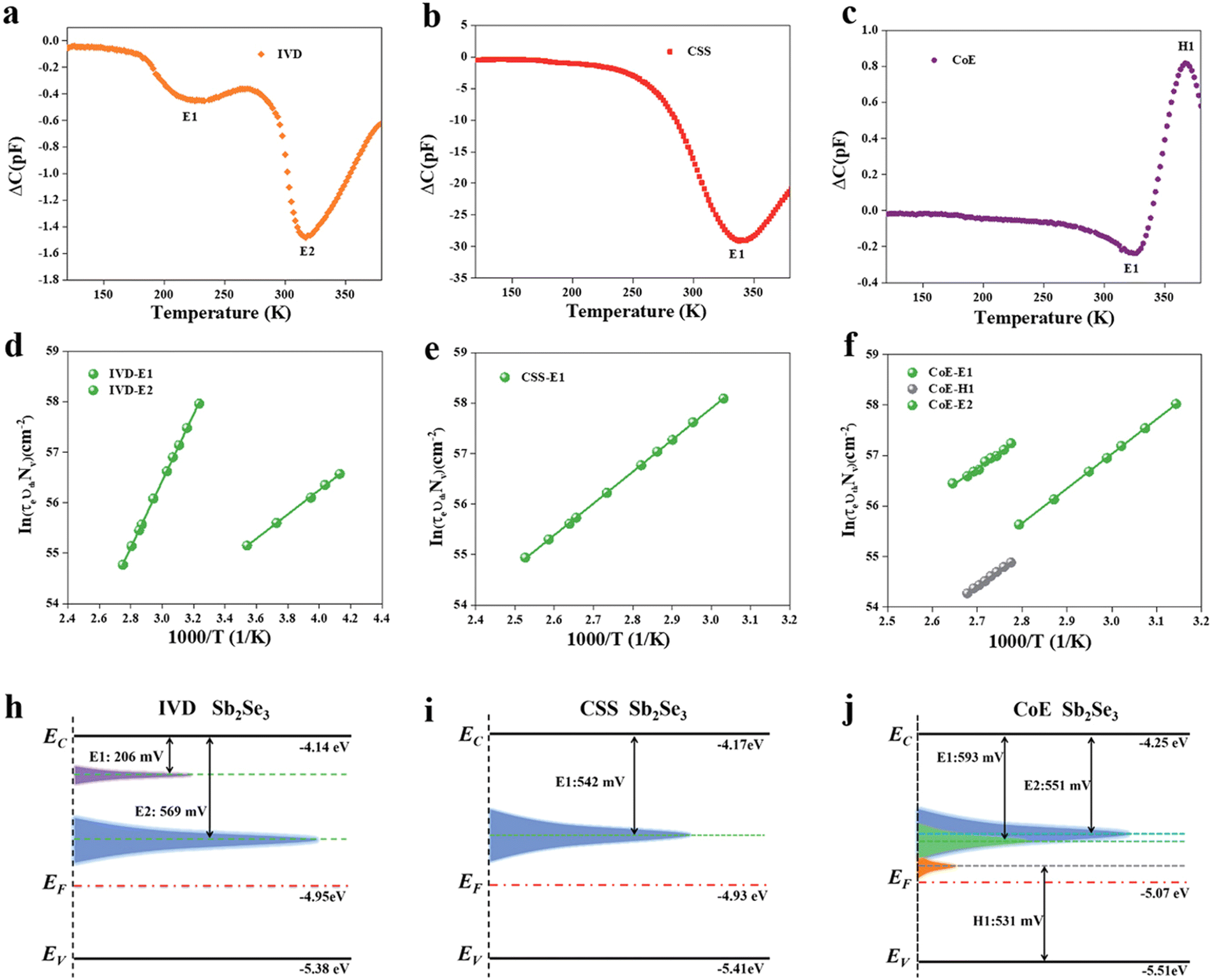 | ||
| Fig. 10 DLTS analysis of solar cells based on IVD-, CSS-, and CoE-Sb2Se3 absorbers. DLTS signals of (a) IVD-Sb2Se3, (b) CSS-Sb2Se3, and (c) CoE-Sb2Se3 solar cells. Arrhenius plots obtained from DLTS signals for (d) IVD-Sb2Se3, (e) CSS-Sb2Se3, and (f) CoE-Sb2Se3 solar cells. Deep-level defect profile of (g) IVD-Sb2Se3, (i) CSS-Sb2Se3, and (j) CoE-Sb2Se3 solar cells. Adapted with permission from ref. 91 Copyright 2022, Wiley-VCH. | ||
Liu et al.86 employed the controlled co-sublimation of mixed Sb2Se3 and Sb2S3 powders to deposit Sb2(S,Se)3 films, with a V-shape (graded) bandgap. In contrast to the most widely used hydrothermal deposition method for Sb2X3 films, CSS deposition offers the key advantages of fast deposition rates (≈μm min−1), large-area film uniformity, high throughput, and scalability for commercial manufacturing. In this work, instead of the toxic CdS, compact TiO2 was used as the ETL and record PCE value of 9.02% was obtained for the CdS-free Sb2X3 solar cells. An increment in the S/Se ratio was found to be successful in improving the grain size and favorable [hk1]-orientations, simultaneously suppressing the detrimental bulk defects in the Sb2(S,Se)3 films. The incorporation of S in Sb2(S,Se)3 enlarged the band gap and Vbi, both contributing to the enhancement in VOC. The TPV decay measurement revealed carrier recombination lifetimes of 5.47 ms, 6.24 ms, and 3.27 ms in the devices employing Sb2Se3, Sb2(S,Se)3-47%, and Sb2(S,Se)3-76% films, respectively. The electron-only devices were fabricated with the architecture of FTO/TiO2/Sb2(S,Se)3/PCBM/Ag, and lower VTFL (and NT) was obtained in the Sb2(S,Se)3-47% based device than its counterparts. The capacitance-frequency analysis revealed NT values of 8.49 × 10¹⁵ and 1.08 × 1016 cm−3 in the Sb2(S,Se)3-47% and Sb2(S,Se)3-76% films, respectively. The DLTS signal for the Sb2(S,Se)3-47% device revealed two negative peaks, which were attributed to two minority (hole) traps, i.e., H1 and H2 (both assigned to SbS antisite defects) (Fig. 11d). Alternatively, the Sb2(S,Se)3-76% device exhibited one electron trap (E1, SSb) and one hole trap (H2, SbS) (Fig. 11g). Particularly, the E1 and H2 traps were located close to the EF-level, and thus highly effective in EF-level pinning and concomitant VOC deficit. It was speculated that an increase in S-content induced SSb antisite defects. Furthermore, a lower S-content passivated the VSe defects and inhibited the SbS defect density in the Sb2(S,Se)3 absorber films.
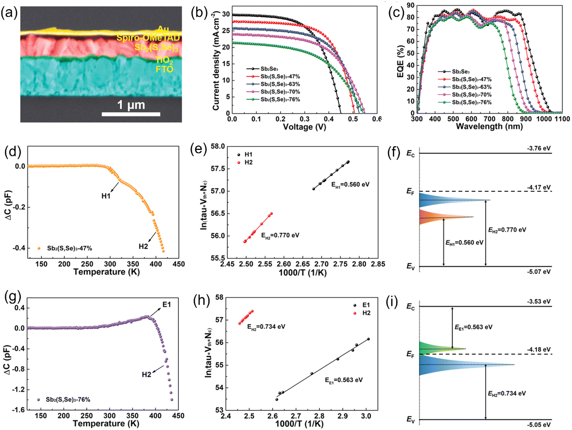 | ||
| Fig. 11 (a) Cross-sectional SEM image of the Sb2(S,Se)3 solar cells. (b) Current density–voltage (J–V) curves and (c) external quantum efficiency (EQE) spectra of the Sb2(S,Se)3 solar cells with different S-contents. (d) and (g) DLTS signals and (e) and (h) Arrhenius plots obtained from the DLTS signals. (f) and (i) Conduction (EC), valence (EV) band edges, Fermi (EF), and defect energy levels of the Sb2(S,Se)3 films with 47% and 76% S-content, respectively. Adapted with permission from ref. 86 Copyright 2022, Wiley-VCH. | ||
Han et al.93 investigated the role of post-annealing SbCl3 treatment on Sb2S3 thin films and the corresponding solar cells (FTO/TiO2/Sb2S3/spiro-OMeTAD/Au). The hole trap density was investigated by analyzing the dark J–V characteristics of the hole-only device (FTO/PEDOT:PSS/Sb2S3/spiro-OMeTAD/Au). Fig. 12(e) indicates the linear response of all the hole-only devices at low voltages treated with different concentrations of SbCl3. On exceeding the kink point (referred to as trap field limit voltage, VTFL), the current demonstrated a non-linear increase, suggesting that the trap states were filled by the injected carriers. The trap density (NT) depends linearly on VTFL (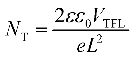 , where e is the elementary charge of the electron, L is the Sb2S3 film thickness, ε (= 6.67) is the relative permittivity of Sb2S3, and ε0 is the vacuum permittivity). The VTFL of the control device was 0.75 V, corresponding to a trap-state density of 2.81 × 1016 cm−3. An increase in the SbCl3 concentration from 15 to 30 mg mL−1 led to a decrease in VTFL from 0.57 to 0.40 V, and NT from 2.13 × 10¹⁶ to 1.50 × 1016 cm−3. A further increase in SbCl3 concentration to 60 mg mL−1 led to an increase in VTFL to 0.65 V and NT to 2.43 × 1016 cm−3. The TPC and TPV decay were analyzed under short-circuit conditions and open-circuit voltage to reveal the influence of SbCl3 treatment on the charge transfer and recombination lifetimes, respectively. Compared to the control device (1.03 μs), the devices treated with 30 mg mL−1 SbCl3 demonstrated the most efficient charge transfer (0.31 μs). The same device also exhibited a lengthier carrier recombination lifetime (89.34 μs) than the control devices (28.35 μs). The ideality factor (η) for the control device (1.71) dropped to the lowest value of 1.59 in the case of 30 mg mL−1 SbCl3 treatment. All these results unambiguously suggest inhibited SRH recombination in the device with 30 mg mL−1 SbCl3 treatment, delivering a PCE of 7.10% (outperforming the control device with a PCE of 4.37%). Li et al.94 fabricated electron-only devices (FTO/buffer layer/CdS/Sb2S3/PCBM/Ag) to estimate the (electron) trap density in the Sb2S3 layer. VTFL values of 0.69, 0.39, and 0.29 V were calculated for the devices without, with SnO2, and with Mg-doped SnO2 as the buffer layers, respectively. Estimated trap densities of 5.66 × 10¹⁵, 3.2 × 10¹⁵ and 2.38 × 1015 cm−3 were obtained in the corresponding devices, respectively. The reduction in trap states was attributed to the lowering of the lattice mismatch at CdS/Sb2S3 on introducing the buffer layers and suppression of the grain boundary defects.
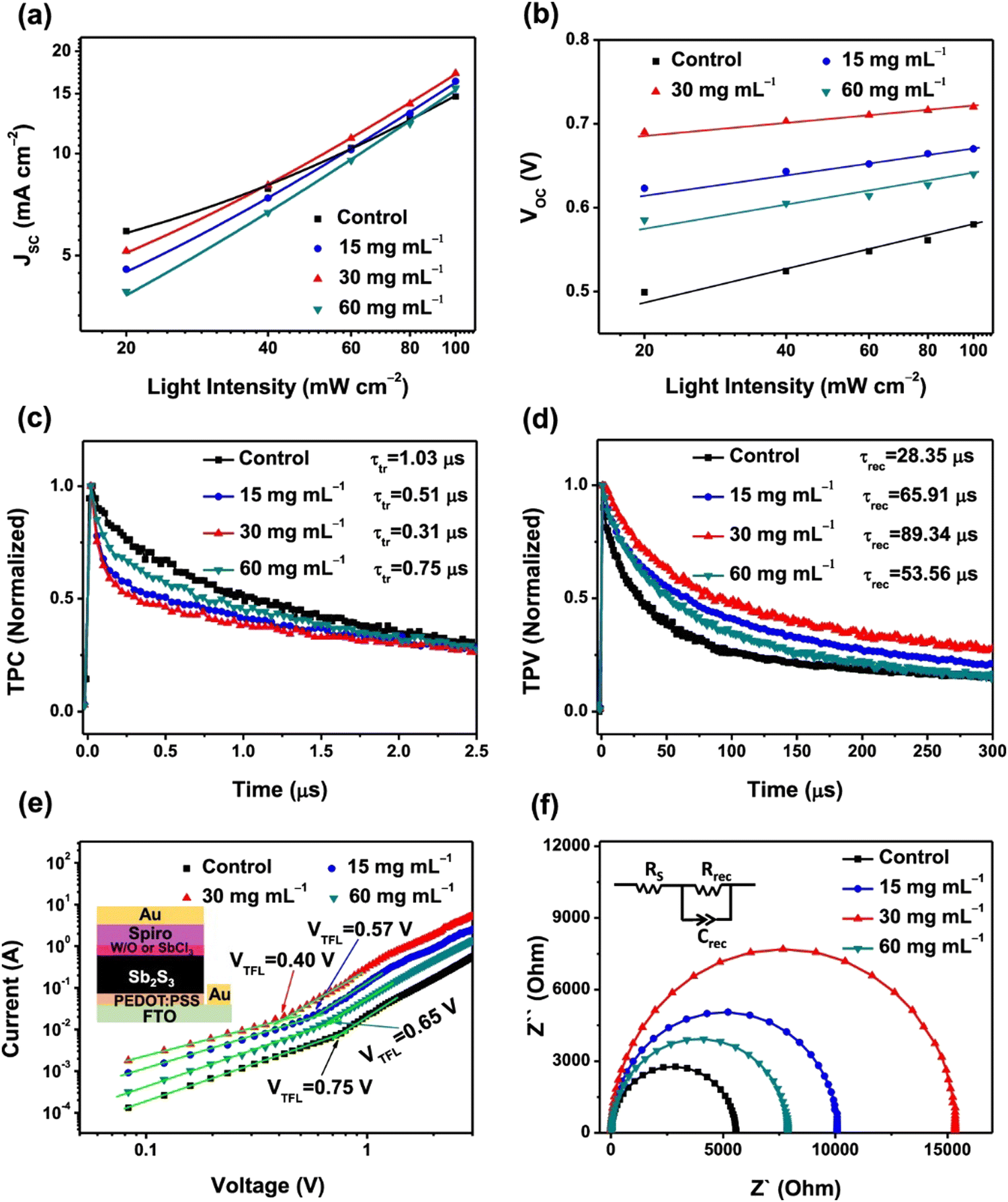 | ||
| Fig. 12 (a) JSC and (b) VOC as a function of light intensity in the control Sb2S3 and SbCl3-treated Sb2S3 devices with different SbCl3 concentrations. (c) TPC and (d) TPV decay characteristics of the control Sb2S3 and SbCl3-treated Sb2S3 devices. (e) Dark J–V measurements of the hole-only devices, revealing VTFL kink point behavior. (f) Nyquist plots for the devices measured in the dark at an applied voltage close to the VOC (inset: equivalent circuit diagram employed to fit the Nyquist plots). Adapted with permission from ref. 93 Copyright 2020, the American Chemical Society. | ||
Hu et al.88 systematically identified and characterized the defects in Sb2Se3 solar cells using temperature-dependent admittance spectroscopy measurements. DC reverse bias-dependent admittance measurements (in the frequency range 20–105 Hz) revealed the presence of three types of defects with energy levels varying in the range of 0.3–0.4, 0.2–0.6 and 0.5–0.6 eV above the VBM, which were denoted as D1, D2, and D3, respectively. D1 and D2 were identified as bulk defects, while D3 as an interface or near-interface defect. D1 exhibited a large cross-section, but low trap density, leading to moderate (∼μs) carrier lifetimes for holes. D2 was assigned as a shallow acceptor level, with an insignificant capture cross-section (10−20 cm2) and lengthier (∼ms) carrier-lifetimes for holes. D3 exhibited a large cross-section for holes, in conjugation with high defect density, leading to short lifetimes for holes (∼ns), thus serving as a prominent recombination center. Pan et al.87 performed quantitative investigation of the majority carrier defect density in all vacuum-deposited Sb2(S,Se)3 solar cells via the admittance spectroscopy technique. The Ea values of the devices with CSS- and CBD-CdS were 203 and 364 meV, respectively. Two-hole traps (H1 and H2) were identified, which were attributed to VSe and SbSe defects, respectively. The Sb2(S,Se)3 device with CBD-CdS (PCE of 5.05%) exhibited a higher defect density, capture cross-section and shorter capture lifetime than its CSS-CdS counterpart (PCE of 7.12%). According to this study, it was concluded that the PCE of state-of-the-art Sb2X3 solar cells can be improved by adopting higher crystallinity CSS-CdS films as the ETL instead of the widely used CBD-CdS films.
Li et al.95 fabricated an Sb2Se3/CdS core–shell structured nano-array solar cell, with a record FF of 70.3% and PCE of 9.2% (Fig. 13d). Briefly, [001]-oriented Sb2Se3 nano-arrays were deposited using CSS and a four-step model was proposed for the growth of Sb2Se3 nanorods on an Mo/MoSe2 substrate including surface absorption, film growth, splitting, and nanorod array growth stage. DLCP measurements suggested that the Sb2Se3 films deposited using CSS had a lower bulk-defect density (Nd of ∼ 2 × 1015 cm−3) than the thermally evaporated films (Nd of ∼ 2 × 1017 cm−3). Capacitance–voltage (C–V) profiling suggested that the Sb2Se3/CdS core–shell interface was much more defective (interface defect density of ∼ 3 × 1012 cm−2) than the planar CdS/Sb2Se3, ZnO/Sb2Se3 or TiO2/Sb2Se3 interfaces in the superstrate configurations. An ultrathin ALD-grown TiO2 layer was used at the Sb2Se3/CdS interface to passivate the surface defects in the Sb2Se3 layer and suppress the detrimental current-leakage paths. Furthermore, as illustrated in Fig. 13(e), the champion device exhibited an excellent EQE (>85%, between 550 and 900 nm), suggesting efficient long-range carrier transport along the [001]-direction.
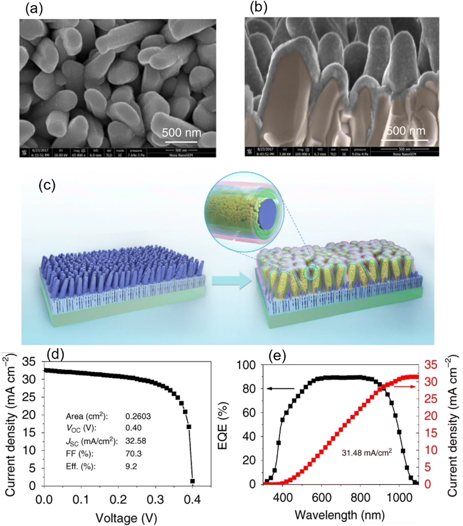 | ||
| Fig. 13 (a) Top-view and (b) cross-sectional SEM images of CdS buffer deposited on Sb2Se3 nanorod arrays. (c) Schematic of the Sb2Se3 nanorod arrays on Mo-coated glass and fabricated Sb2Se3/CdS (core/shell) nanorod array solar cells. (d) J–V curve and (e) EQE spectrum and integrated JSC curve of the champion device. Adapted under the guidelines of the Creative Commons BB CY license from ref. 95 Copyright 2019, Springer Nature. | ||
4. Strategies toward high PCE Sb2X3 solar cells
4.1. Deep-level defect passivation and EF-level depinning in photoactive Sb2X3 films
Mitigating deep-defects (particularly that with a large capture cross section) is a crucial strategy to elevate the minority carrier lifetime and boost the VOC (and PCE) of fabricated Sb2X3 solar cells. A short lifetime (∼0.01–1 ns) and long lifetime (∼5–60 ns) are commonly observed in Sb2X3 solar cells.29 The former is attributed to interface recombination, while the latter to bulk recombination. Yang et al.34 studied the (longer) carrier lifetimes in an Sb2S3 thin film and single crystal using TAS and concluded that the longer lifetime originates from the self-trapped exciton (STE) owing to the soft lattice in Q-1D-structured Sb2X3. The device PCE (and VOC) was constrained by the shortest lifetimes. The simulation results revealed that 2 orders of magnitude improvement in carrier lifetime can gain an ∼150 mV increase in VOC in Sb2X3 solar cells, as illustrated in Fig. 14.29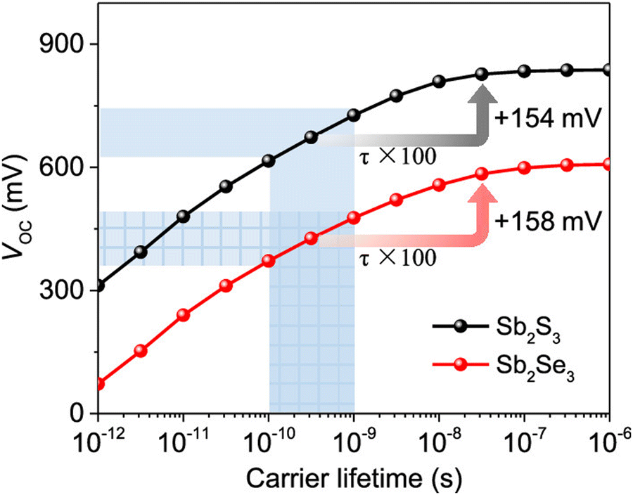 | ||
| Fig. 14 Simulated VOC of Sb2S3 and Sb2Se3 solar cells as a function of carrier lifetime by SCAPS. The shadow area exhibits the generally accepted lifetimes and VOC of the Sb2S3 and Sb2Se3 solar cells. Adapted with permission from ref. 29 Copyright 2020, the American Chemical Society. | ||
As shown in Fig. 15(a), a high density of multiple types of deep traps exists in Sb2X3 thin films. These traps serve as scavengers for photogenerated carriers and accelerate trap-assisted SRH recombination, and thus detrimental to the performance of Sb2X3 solar cells. Solution-processed Sb2X3 films usually contain a minuscule amount of oxide impurities (mainly Sb2O3). These oxide impurities form deep traps, and thus limit the VOC values. In this case, given that Sb2O3 is recognized as a center of electron–hole pair recombination, Sb2O3-free, Sb2X3 films are advantageous for achieving high-performance Sb2X3 solar cells. The Sb2X3 films synthesized using vacuum-assisted techniques are relatively oxide free and exhibit a higher degree of phase purity.96 However, recent studies suggest that controlled O2-incorporation can help in passivating bulk and interface defects, improving the device performance.97 In addition, in situ sulfurization,98,99 post-deposition thioacetamide (TA) treatment,78 ammonium sulfide ((NH4)2S) treatment,77 thiourea (TU) treatment,5 selenization,100–102 alkali-metal doping,103–105 and alcohol-vapor annealing106 are key strategies to passivate deep-defects and boost the PCE of Sb2X3 solar cells.
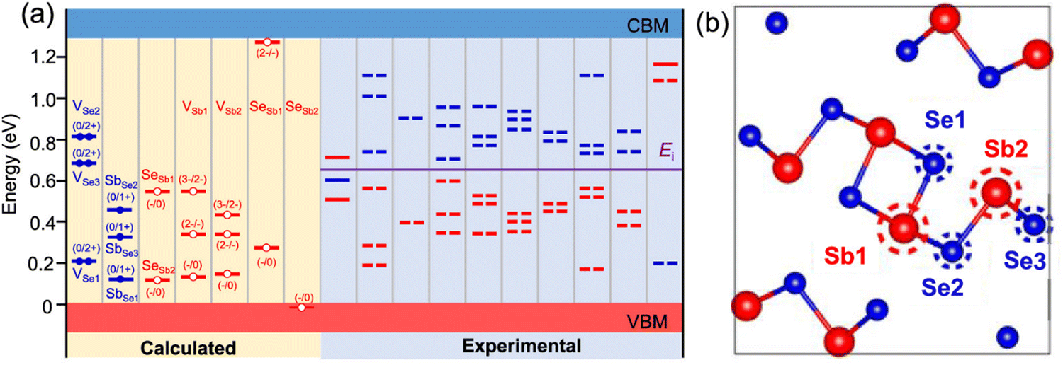 | ||
| Fig. 15 (a) Defects in Sb2Se3 calculated by DFT (left) and probed by DLTS and admittance spectroscopy (right). The middle of the bandgap is denoted as Ei. The red and blue levels represent the acceptor and donor levels, respectively. The defects measured by admittance spectroscopy have no clear acceptor/donor type, and thus two defect levels that are symmetric about the Ei are represented by dashed lines. Adapted with permission from ref. 29 Copyright 2020, the American Chemical Society. (b) Non-equivalent two-Sb and three-Se atomic sites in each (Sb4Se6)n atomic chains. Reproduced with permission from ref. 56 Copyright 2019, the American Chemical Society. | ||
Another issue with Sb2X3 solar cells is Fermi level (EF) pinning by the traps located near the mid-bandgap. Lian et al.74 investigated the deep-level defects in Sb-rich and S-rich Sb2S3 films via O-DLTS. It was revealed that S-vacancy (VS) and Sb-antisite (SbS) are the two main electron traps in S-deficient films. These traps have a high density and capture cross-section and contribute to EF-level pinning. The electron quasi-EF level is pinned by these traps, resulting in the inefficient extraction of trapped photo-exited carriers. S-rich films have two main hole traps, which have been identified as Sb-vacancy (VSb) and S-antisite (SSb). These traps are not electrically active compared to that in S-deficient films. Based on a first principles study, Cai et al.75 and Jiang et al.107 concluded that the formation energies of the dominant acceptor defects (VSb2, SbS2, and SSb2) and donor defect (VS2) in intrinsic Sb2S3 are similar. This results in EF-level pinning at the near-middle of the band gap. These results are in agreement with the experimentally observed high resistivity in undoped Sb2S3 thin films.108 Wen et al.90 attributed the hole quasi EF-level pinning in Sb2Se3 to the [SbSe + SeSb] anti-site complex. In general, these defects exhibit a higher density than the carrier density (∼1013 cm−3) in Sb2Se3 films. These defects are located slightly above the intrinsic EF-level, and thus highly active trap centers; in contrast, the traps below the intrinsic EF-level are occupied, and thus inactive. The VTD process has been found to be more effective in depositing Sb2X3 films with an improved density of [SbSe + SeSb] anti-site pairs, thus depinning the hole quasi EF-level and inducing greater splitting of the quasi- EF-levels during illumination. Sb2X3 films should be made anion (S,Se) rich to passivate the bulk defects and promote the charge transport efficiency.
4.2. Crystallographic orientation engineering
Owing to their unique quasi-1D crystal structure and the associated anisotropy in carrier mobility, the orientation of crystallites/ribbons (schematically illustrated in Fig. 16) plays a decisive role in the device performance. In this case, [hk1]-oriented Sb2X3 films offer excellent carrier transport, suppressed bulk recombination, and trap-free grain boundaries, facilitating high-PCE devices. In this regard, the growth of Sb2X3 should be regulated from the 2D (layer-like) mode to 3D (island-like) mode. Liang et al.109 demonstrated the growth of highly [hk1]-oriented Sb2Se3 nanorod arrays perpendicular to a selenized tungsten (W) back-contact in substrate-structured solar cells. The resulting ultrathin film of tungsten selenide (WSe2) also acted as the HTL, promoting efficient hole extraction, and consequently leading to a PCE of 8.46%. Wang et al.110 reported the preparation of highly [221]-oriented Sb2Se3 films on a randomly oriented ZnO buffer layer. The ZnO layer was deposited via a green and scalable spray pyrolysis technique, and the device demonstrated a low density of interface defects and highly improved efficiency and stability. Zhou et al.111 employed a simple and fast (∼1 μm min−1) RTE process to orient the crystal growth perpendicular to the substrate and produced an Sb2Se3 thin-film solar with a certified PCE of 5.6%. Li et al.112 introduced a seed screening strategy to deposit [211]- and [221]-oriented Sb2Se3 films on a TiO2 film. It was revealed that lying seeds (with [hk0]-orientation) bonded with the substrate through weak vdW forces, while the standing seeds ([hk1]-orientation) bonded with the substrate by covalent bonds. The [hk0]-oriented seeds easily re-evaporated from the TiO2 surface at high substrate temperature, leaving tightly bonded [hk1]-oriented seeds and assisting the growth of [221]- and [211]-oriented Sb2Se3 grains. Liu et al.113 revealed that devices based on thermally deposited hexagonal-CdS outperformed that with solution-processed cubic-CdS. The former was found to be more conducive to the growth of [221]-oriented, compact, and less-defective Sb2X3 films.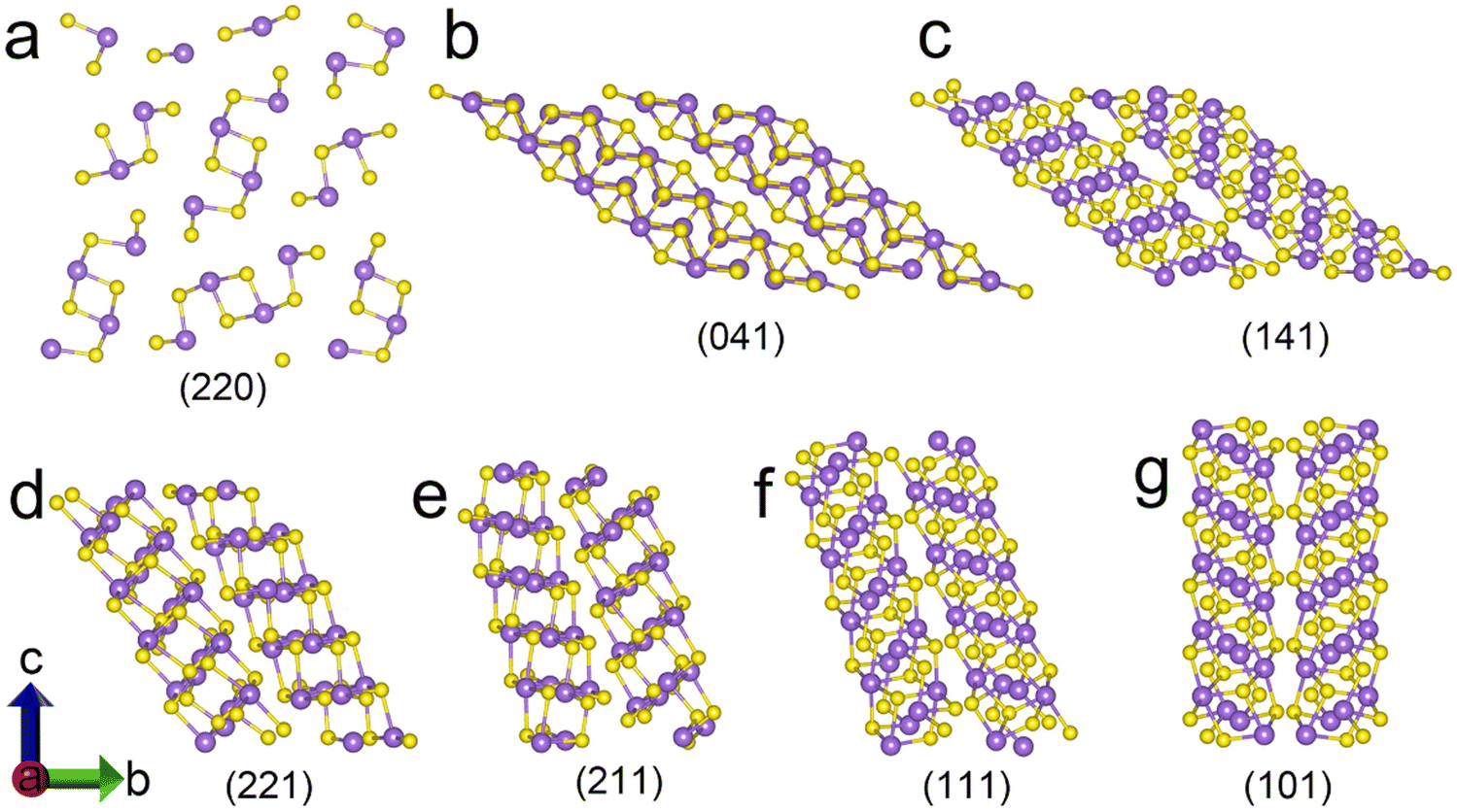 | ||
| Fig. 16 Schematic of the (Sb4S6)n ribbons with different crystal planes (Sb3+ = purple dots and S2+ = yellow dots). Adapted with permission from ref. 1 Copyright 2022, Elsevier Ltd. | ||
Park et al.114 manipulated the microstructure (morphology and crystallite orientation) of the Sb2Se3 absorber layer by regulating the substrate temperature during co-evaporation. Consequently, [hk1]-oriented Sb2Se3 nanopillar arrays were obtained at 315 °C. According to this study, it was concluded that a narrow window exists for the substrate temperature, where vertical [hk1]-oriented Sb2Se3 rod arrays can be grown. The [hk1]-oriented crystallites assist in maximizing the carrier transport characteristics. The dependence of Sb2Se3 microstructures on the substrate temperature was explained using the Terrace-Ledge-Kink model and the nucleation and growth theory. Kondrotas et al.115 studied the growth process of Sb2Se3 on Mo, MoSe2, CdS, ZnO and TiO2 substrates. It was revealed that the slow growth rates on the Mo-substrate led to the deposition of [hk0]-oriented Sb2Se3 layers. In contrast, [hk1]-oriented layers were obtained at high growth rates. Accordingly, it was concluded that for all the vapor-deposited Sb2X3 films, a compact morphology with the desired [hk1]-orientation can be achieved on all the substrates while working in the high growth rate regime window, which is governed by the evolution selection principle. Zhou et al.116 demonstrated that with an increase in the substrate temperature and decrease in the substrate-surface bonding energy, the orientation of Sb2Se3 films can be tailored from [hk0] to [hk1], and ultimately [002]. The change in the orientation from [hk0] to [hk1] modifies the carrier transport from the inter-ribbon (hopping) to intra-ribbon (band-like) mode, improving the carrier collection efficiency. Notably, the [hk1]-oriented Sb2X3 films not only ensured better charge transport, but also bonded strongly with the substrate below (via covalent bonds), in contrast to the [hk0]-oriented films (where ribbons lie flat on the substrate surface and weak van der Waals bonding links the substrate and Sb2X3).
4.3. Grain boundary engineering
Zhao et al.9 demonstrated an outstanding improvement in average grain size in CBD Sb2Se3 films (from 170 to 435 nm) by using additives to manipulate the reaction kinetics and deposition process. Wang et al.117 developed a fast chemical approach (FCA) for spin coating Sb2S3 films with an average grain size exceeding 12 μm. Han et al.106 revealed that alcohol vapor (ethanol, methanol, and isopropanol) post-annealing induces a significant enhancement in the crystallinity, morphology and carrier lifetimes of Sb2S3 films (as illustrated in Fig. 17). This annealing strategy improved the charge collection efficiency and PCE of Sb2S3 solar cells. Alcohol vapor induced solvent stitching via partial dissolution of the GBs, creating a melt phase, which acted as a “stitching adhesive” for enhanced grain growth.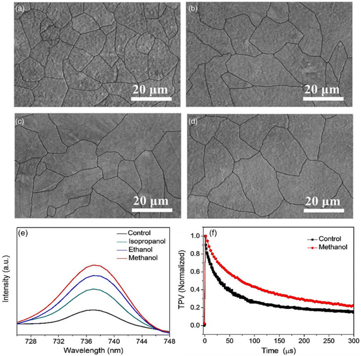 | ||
| Fig. 17 SEM micrographs of (a) control Sb2S3 film, (b) iso-annealed Sb2S3 film, (c) eth-annealed Sb2S3 film, and (d) meth-annealed Sb2S3 film. (e) PL spectra of the control, iso-annealed, eth-annealed, and meth-annealed Sb2S3 films and (f) TPV decay characteristics of the control and meth-annealed Sb2S3 solar cells. Adapted with permission from ref. 106 Copyright 2019, Wiley-VCH. | ||
4.4. Selection of ETL and HTL materials and (ETL/Sb2X3, Sb2X3/HTL) interface engineering
All the high-PCE-Sb2X3 solar cells exclusively use the toxic CdS as the ETL and expensive and long-term unstable Spiro-OMeTAD as the HTL (Table S1, ESI†). In this regard, there have been serious attempts to either substitute CdS and Spiro-OMeTAD completely or reduce their usage. The devices based on an oxide ETL (TiO2, SnO2, and ZnO) underperform (showing an inferior PCE) than their CdS-based counterparts. Doping O118 and Al92 in the CdS layers effectively modifies the band alignment at CdS/Sb2Se3 from a “cliff-like” to “spike-like” alignment, which is well suited for efficient electron extraction. Double buffer layers, e.g., TiO2/CdS,119,120 SnO2/CdS,120,121 Zn(O,S)/CdS,103,122,123 ZnSnO3/CdS,5 Mg:SnO2/CdS,94 and ZnO/TiO2,124 successfully suppresses the shunt paths and improve the cascaded band-alignment for efficient carrier transport. Han et al.125 demonstrated the synergistic role of zinc halide (ZnCl2, ZnBr2, and ZnI2) treatment of TiO2 in modifying the TiO2 layer and TiO2/Sb2S3 interface. In particular, ZnCl2 treatment curtailed the roughness and trap density in a TiO2 film, simultaneously increasing the electron concentration and mobility in the layer. The improvement in the TiO2/Sb2S3 interface quality and device performance on ZnCl2 treatment were mainly attributed to the passivation of undercoordinated Ti4+ and O2− (on TiO2 surface) by coordinating with Cl− and Zn2+, respectively, and improved crystallinity of Sb2S3 film (with enlarged grains and diminished trap states). Zn(O,S) has emerged as a promising ETL for Sb2X3 solar cells, given that the S-atoms (at the surface of Zn(O,S)) serve as chemical bridge to facilitate the quasi-epitaxial growth of Sb2X3 films.50,126 The quasi-vertical growth of [211]- and [121]- oriented Sb2S3 films has been found to be conducive on CdS substrates, whereas the S-deficit on the CdS surface creates a beneficial bonding environment between the exposed undercoordinated Cd2+ and S atoms in the Sb2S3 molecules.127 Also, the [101]-facet grains of TiO2 has been found to be effective in inducing the quasi-epitaxial growth of [hk1]-oriented Sb2S3 films.128 Solution processing has been found to be successful in the growth of Sb2S3 monolayers (with preferentially oriented, single-crystalline cuboids) on TiO2 nanoparticle films (schematically presented in Fig. 18).129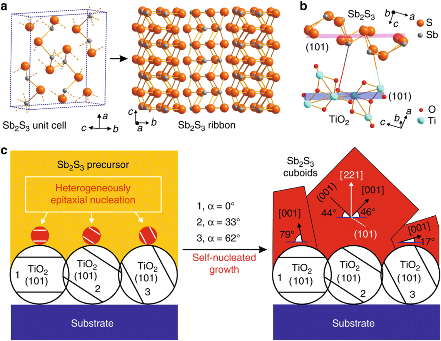 | ||
| Fig. 18 Schematic illustrations of (a) orthorhombic crystal structure of Sb2S3, consisting of (Sb4S6)n ribbons stacked parallel to the [001] direction. (b) Atomic configuration at the Sb2S3/TiO2 interface. (101) planes of Sb2S3 grow epitaxially over anatase TiO2 template. (c) Nucleation/growth model for the growth of Sb2S3 single-crystalline cuboids on TiO2 nanoparticle film. The most competitive TiO2 nanoparticle orientation for the Sb2S3 single-crystals to nucleate/grow features its (101) plane tilting at an angle (α) on the substrate plane close to α = 33° (particle 2), but the nucleation/growth at the other sites around (e.g., particle 1 of α = 0° and particle 3 of α = 62°) is relatively much slower or suppressed due to their unfavorable TiO2 (101) plane orientations. Adapted under the guidelines of the Creative Commons CC BY license from ref. 129 Copyright 2019, Springer Nature. | ||
Li et al.130 skillfully utilized Cu-diffusion (from CuSCN) in the Sb2Se3 absorber layer. This diffusion not only inverted the GBs (in Sb2Se3) but also increased p-type doping in CuSCN (owing to the increment in VCu, which acts as shallow acceptors). CuSCN has been found to successfully improve the built-in potential and carrier collection efficiency and alleviate the back surface recombination losses. CuSCN and CuSbSe2 have emerged as the top choice as the HTL in Sb2X3 solar cells, owing to the negligible lattice mismatch and lower trap density at the CuSCN/Sb2X3 and CuSbSe2/Sb2X3 interfaces. MnS has shown promising results as the HTL in Sb2X3 solar cells, with a better performance compared to its spiro-OMeTAD-based counterparts in terms of PCE and stability. Furthermore, owing to the better band-alignment (with Sb2X3), physicochemical robustness, and low price (4$ per g) of MnS, it seems to be a better alternative to Spiro-OMeTAD powder (500$ per g) in Sb2X3 solar cells.131 Liu et al.132 employed an ultrathin poly(methyl methacrylate) (PMMA) film as a hole-selective tunneling layer to modify the Sb2S3/spiro-OMeTAD interface in Sb2S3-based nano-array solar cells. As illustrated in Fig. 19, the PMMA layer was found to be effective in blocking the interfacial recombination channels and boosting the overall device performance.
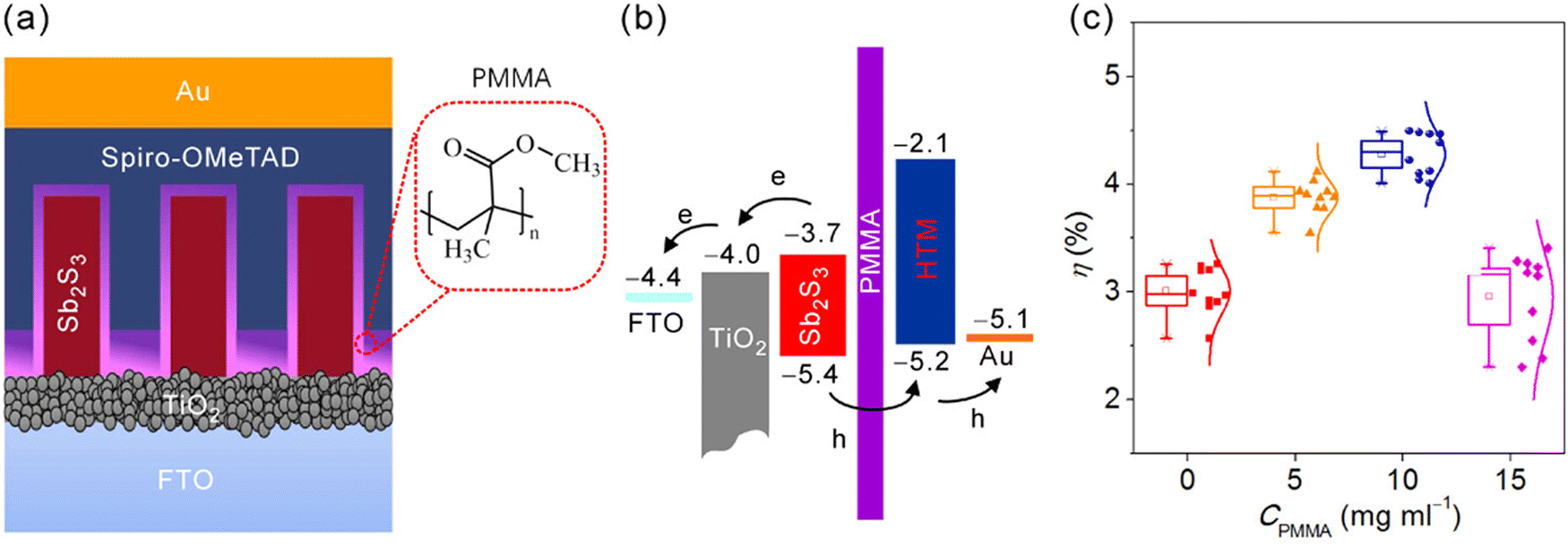 | ||
| Fig. 19 Schematic of (a) configuration of the Sb2S3/TiO2 nano-array solar cell with PMMA interfacial layer and (b) its energy level diagram. (c) Statistical distribution of PCE (η) without (CPMMA = 0 mg mL−1) and with (CPMMA = 5, 10 and 15 mg mL−1) PMMA interfacial layer, illustrating the dependence of the device performance on PMMA concentration. Adapted with permission from ref. 132 Copyright 2023, the American Chemical Society. | ||
SbCl3 treatment has been used in the fabrication of Sb2S393 and Sb2Se3133 solar cells. SbCl3 treatment of Sb2S3 films was found to be highly effective in mitigating the trap states (at the interface and grain boundaries) and suppressing the non-radiative recombination. This strategy was successful in simultaneously improving the PCE and stability of Sb2S3 solar cells. In the case of Sb2Se3 solar cells, SbCl3 treatment (on the CdS layer) improved the morphology of the CdS layer, transformed the band-offset at CdS/Sb2Se3 from cliff-like to spike-like, and induced [hk1]-oriented growth in Sb2Se3 films. It was found that 1 nm thick (and sputtered) Si3N4134 and 2 nm thick (and evaporated) CeO2135 ultrathin interface layers (sandwiched between CdS and Sb2Se3) showed promising results in inducing columnar [hk1]-oriented growth, ameliorating the crystallinity and surface evenness of Sb2Se3 thin films. Controlled oxygen doping in CdS (O:CdS) has been found to be successful in suppressing parasitic absorption (by CdS layer), improving the CdS/Sb2Se3 band-alignment, mitigating the interface recombination and improving electron transport.136 Potassium doping in CdS (K:CdS) has been reported to simultaneously improve the crystallinity of CdS and Sb2S3 films, decreasing the surface roughness of Sb2S3 films and improving all the device parameters of Sb2S3 solar cells. An ultrathin PbS interface layer successfully formed an Sb–S–Pb bonding bridge and cascaded band alignment, accelerating the hole transport and inhibiting carrier recombination at the Sb2(S,Se)3/carbon interface.137
4.5. Doping strategies
The low built-in potential caused by a low intrinsic doping density (∼1012 cm−3) and poor carrier collection efficiency due to sluggish carrier mobility lead to a mediocre performance in Sb2X3 solar cells. However, efficient doping in Sb2X3 is very challenging. Owing to the distinctive Q-1D structure, the dopant atoms commonly settle in the inter-ribbon space or at the GBs and become electrically inactive. Ti138 and Zn139 doping has been shown to be successful in improving the crystallinity and absorbance of Sb2S3 thin films, leading to a higher Jsc in Sb2S3 solar cells. Particularly, Zn doping was found to successfully boost the carrier (electron) concentration in Sb2S3 films and solar cell performance. Zn was found to coordinate with S at the grain boundaries. The low hole mobility in the pristine Sb2S3 film was elevated from 1.0 cm2 V−1 s−1 to 205 cm2 V−1 s−1 on Sn-doping.140 Ni-doped Sb2S3 films demonstrated better photon harvesting than pristine Sb2S3 films. Ag,141 Co,142 Mn,143 Sm,144 Fe,142 Cu,145 Sn,146 Bi,147 Se,148 and alkali metal (Li, Na, K, Rb, and Cs)149 doping has also been found to successfully enhance the carrier density and conductivity in Sb2S3 films.150–152 Ni settled at the grain boundaries and formed NixSy at lower temperatures, which provided nucleation centers for the [hk1]-oriented growth of Sb2S3 ribbons.153 An improvement of up to six orders in p-type conductivity (from 10−8 to 10−2 S cm−1) was demonstrated in Sb2S3 films on C doping.154 The increased electrical conductivity was attributed to the formation of CS substitutional defects in the Sb2S3 crystal structure. C doping has also been used to implement p+ doping in Sb2(S,Se)3 films.155Pb doping has been shown to successfully enhance the carrier (hole) concentration and conductivity of Sb2Se3 films by four and three orders, respectively.156 The Sb3+ in the Sb2Se3 crystal was partially replaced by Pb2+, forming acceptor energy levels for effective hole-doping. I doping induced n-doping in Sb2Se3via substitution of Se by the I atoms, leading to a one order increase in conductivity.157 An improvement of three orders in p-type conductivity and four orders in hole density in Sb2Se3 films was obtained on Sn doping.157 The conductivity of Sb2Se3 films slightly improved upon doping with transition metals and lanthanides (Lu3+, Ho3+, Nd3+, Sm3+, and Gd3+) and co-doping with Lu3+/Yb3+ and Lu3+/Er3+.158,159 Fe doping in Sb2Se3 was found to improve the carrier concentrations and mobility of the majority carriers. Costa et al.160 reported that Fe:Sb2Se3 films exhibit p-type conductivity, while Li et al.161 reported that these films have n-type conductivity. Te doping has been implemented to introduce n-type doping in Sb2Se3 films. Te:Sb2Se3 films were deposited via thermal evaporation,162 sputtering,163 and spin coating.92 However, three independent studies suggested the Te-dopant settled at the lattice in the inter ribbon spacing and in the grain boundaries, respectively. S,92 Na164 and Mg161 doping has also been implemented in Sb2Se3 thin films. S substitutes Se in the lattice, while Na and Mg prefer to settle in the grain boundaries or inter-ribbon space (where they are electrically inert).
5. Concluding remarks
Considering the overall assessment, the expanding toolbox of defect-engineering strategies is anticipated to play a pivotal role in the foreseeable development of Sb2X3 PV. The dominant deep-level defects in Sb2X3 solar cells are anion-vacancies (VS and VSe) and cation anti-sites (SbS and SbSe). It seems conceivable that the regulation of S/Se volatilization (especially during the annealing step) is the key to controlling the deep defects. The high formation energy of VS/Se induces (thermally driven) the migration of neighboring Sb atoms to form SbS/Se defects. Therefore, controlled annealing of as-deposited (amorphous) films under an S/Se-rich environment or in an H2S/CS2 environment can be a straightforward strategy to passivate VS/Se before they transform into detrimental SbS/Se defects. Exploring novel low-temperature synthesis protocols for the synthesis of Sb2X3 films can also be instrumental in curtaining the anti-site defects. Nanocrystal seed- and seed-layer assisted growth has also been found to successfully deposit Sb2X3 films with desirable characteristics. Vapor transport deposition techniques have been found to be more effective in depositing Sb2X3 films with diminished anti-site defects compared to the conventional thermal evaporation and solution processing methods. A slight S/Se-rich stoichiometry and [hk1]-oriented growth are crucial for obtaining Sb2X3 films with a low-defect density, better photoconductivity and adhesion with the substrates than S/Se-deficient and [hk0]-oriented films. In addition, doping strategies, and halide salt treatment of ETL/Sb2X3 and Sb2X3/HTL interfaces have also been found to be instrumental in regulating the defect dynamics and PV performance. This work is anticipated to spur greater control of the engineering of deep defects in Sb2X3 thin films, eliminating their adverse effects on the device performance and fabrication of efficient Sb2X3 solar cells.Author contributions
S. B. – conceptualization, drafting original manuscript. S. S. – visualization, methodology. A. K. C. – writing, editing. N. S. P. – reviewing, editing, formatting. A. G. P. – methodology, editing, K. R. – funding acquisition, supervision.Conflicts of interest
There are no conflicts to declare.Acknowledgements
S. B. acknowledges Dr Ramashanker Gupta for his valuable insights and constructive feedback that led to the drafting of the final manuscript. This work received no specific grant from any funding agency in the public, commercial, or not-for-profit sectors.References
- L. Q. Yao, L. M. Lin, Z. P. Huang, Y. Mao, H. Li, W. W. Lin, S. Y. Chen, Z. G. Huang, J. M. Li and G. L. Chen, A Liquid Medium Annealing Strategy for Highly [041]/[141]-Oriented Planar Antimony Sulfide Solar Cells with 7.23% Efficiency, Nano Energy, 2023, 106, 108064, DOI:10.1016/j.nanoen.2022.108064
.
- K. C. Gödel, Y. C. Choi, B. Roose, A. Sadhanala, H. J. Snaith, S. Il Seok, U. Steiner and S. K. Pathak, Efficient Room Temperature Aqueous Sb2S3 Synthesis for Inorganic–Organic Sensitized Solar Cells with 5.1% Efficiencies, Chem. Commun., 2015, 51(41), 8640–8643, 10.1039/C5CC01966D
- K. C. Gödel, B. Roose, A. Sadhanala, Y. Vaynzof, S. K. Pathak and U. Steiner, Partial Oxidation of the Absorber Layer Reduces Charge Carrier Recombination in Antimony Sulfide Solar Cells, Phys. Chem. Chem. Phys., 2017, 19(2), 1425–1430, 10.1039/C6CP07559B
- S. Rijal, A. Adhikari, R. A. Awni, C. Xiao, D.-B. Li, B. Dokken, A. Ellingson, E. Flores, S. S. Bista, D. Pokhrel, S. Neupane, R. E. Irving, A. B. Phillips, K. Jungjohann, C.-S. Jiang, M. Al-Jassim, R. J. Ellingson, Z. Song and Y. Yan, Post-Annealing Treatment on Hydrothermally Grown Antimony Sulfoselenide Thin Films for Efficient Solar Cells, Sol. RRL, 2022, 2201009, DOI:10.1002/solr.202201009
- Y. Qi, Y. Li and Q. Lin, Engineering the Charge Extraction and Trap States of Sb2S3 Solar Cells, Appl. Phys. Lett., 2022, 120(22), 221102, DOI:10.1063/5.0094091
- X. Wang, A. M. Ganose, S. R. Kavanagh and A. Walsh, Band versus Polaron: Charge Transport in Antimony Chalcogenides, ACS Energy Lett., 2022, 7(9), 2954–2960, DOI:10.1021/acsenergylett.2c01464
- Z. Jia, M. Righetto, Y. Yang, C. Q. Xia, Y. Li, R. Li, Y. Li, B. Yu, Y. Liu, H. Huang, M. B. Johnston, L. M. Herz and Q. Lin, Charge-Carrier Dynamics of Solution-Processed Antimony- and Bismuth-Based Chalcogenide Thin Films, ACS Energy Lett., 2023, 8(3), 1485–1492, DOI:10.1021/acsenergylett.3c00140
- S. Wang, Y. Zhao, B. Che, C. Li, X. Chen, R. Tang, J. Gong, X. Wang, G. Chen, T. Chen, J. Li and X. Xiao, A Novel Multi-Sulfur Source Collaborative Chemical Bath Deposition Technology Enables 8%-Efficiency Sb2S3 Planar Solar Cells, Adv. Mater., 2022, 34(41), 2206242, DOI:10.1002/adma.202206242
- Y. Zhao, S. Wang, C. Li, B. Che, X. Chen, H. Chen, R. Tang, X. Wang, G. Chen, T. Wang, J. Gong, T. Chen, X. Xiao and J. Li, Regulating Deposition Kinetics via a Novel Additive-Assisted Chemical Bath Deposition Technology Enables Fabrication of 10.57%-Efficiency Sb2Se3 Solar Cells, Energy Environ. Sci., 2022, 15(12), 5118–5128, 10.1039/D2EE02261C
- X. Chen, B. Che, Y. Zhao, S. Wang, H. Li, J. Gong, G. Chen, T. Chen, X. Xiao and J. Li, Solvent-Assisted Hydrothermal Deposition Approach for Highly-Efficient Sb2(S,Se)3 Thin-Film Solar Cells, Adv. Energy Mater., 2023, 13(21), 2300391, DOI:10.1002/aenm.202300391
- C. Qian, K. Sun, J. Cong, H. Cai, J. Huang, C. Li, R. Cao, Z. Liu, M. Green, B. Hoex, T. Chen and X. Hao, Bifacial And Semitransparent Sb2(S,Se)3 Solar Cells for Single-Junction And Tandem Photovoltaic Applications, Adv. Mater., 2023, 35(42), 2303936, DOI:10.1002/adma.202303936
- J. Zhang, W. Lian, Y. Yin, X. Wang, R. Tang, C. Qian, X. Hao, C. Zhu and T. Chen, All Antimony Chalcogenide Tandem Solar Cell, Sol. RRL, 2020, 4(4), 2000048, DOI:10.1002/solr.202000048
- C. Wang, S. Lu, S. Li, S. Wang, X. Lin, J. Zhang, R. Kondrotas, K. Li, C. Chen and J. Tang, Efficiency Improvement of Flexible Sb2Se3 Solar Cells with Non-Toxic Buffer Layer via Interface Engineering, Nano Energy, 2020, 71, 104577, DOI:10.1016/j.nanoen.2020.104577
- K. Li, F. Li, C. Chen, P. Jiang, S. Lu, S. Wang, Y. Lu, G. Tu, J. Guo, L. Shui, Z. Liu, B. Song and J. Tang, One-Dimensional Sb2Se3 Enabling Ultra-Flexible Solar Cells and Mini-Modules for IoT Applications, Nano Energy, 2021, 86, 106101, DOI:10.1016/j.nanoen.2021.106101
- X. Liang, Y. Feng, W. Dang, H. Huang, X. Wang, Y. Guo, K. Shen, R. E. I. Schropp, Z. Li and Y. Mai, High-Efficiency Flexible Sb2Se3 Solar Cells by Back Interface and Absorber Bulk Deep-Level Trap Engineering, ACS Energy Lett., 2023, 8(1), 213–221, DOI:10.1021/acsenergylett.2c02066
- Z. Su, J. M. R. Tan, X. Li, X. Zeng, S. K. Batabyal and L. H. Wong, Cation Substitution of Solution-Processed Cu2ZnSnS4 Thin Film Solar Cell with over 9% Efficiency, Adv. Energy Mater., 2015, 5(19), 1500682, DOI:10.1002/aenm.201500682
- H. Deng, Y. Cheng, Z. Chen, X. Lin, J. Wu, Q. Zheng, C. Zhang and S. Cheng, Flexible Substrate-Structured Sb2S3 Solar Cells with Back Interface Selenization, Adv. Funct. Mater., 2023, 2212627, DOI:10.1002/adfm.202212627
- S. Barthwal, R. Kumar and S. Pathak, Present Status and Future Perspective of Antimony Chalcogenide (Sb2 × 3) Photovoltaics, ACS Appl. Energy Mater., 2022, 5(6), 6545–6585, DOI:10.1021/acsaem.2c00420
- J. Dong, Y. Liu, Z. Wang and Y. Zhang, Boosting VOC of Antimony Chalcogenide Solar Cells: A Review on Interfaces and Defects, Nano Select, 2021, 2(10), 1818–1848, DOI:10.1002/nano.202000288
- R. Kondrotas, C. Chen and J. Tang, Sb2S3 Solar Cells, Joule, 2018, 2(5), 857–878, DOI:10.1016/j.joule.2018.04.003
- U. A. Shah, S. Chen, G. M. G. Khalaf, Z. Jin and H. Song, Wide Bandgap Sb2S3 Solar Cells, Adv. Funct. Mater., 2021, 31(27), 2100265, DOI:10.1002/adfm.202100265
- M. A. Farhana, A. Manjceevan and J. Bandara, Recent Advances and New Research Trends in Sb2S3 Thin Film Based Solar Cells, J. Sci.: Adv. Mater. Devices, 2023, 8(1), 100533, DOI:10.1016/j.jsamd.2023.100533
- H. Lei, J. Chen, Z. Tan and G. Fang, Review of Recent Progress in Antimony Chalcogenide-Based Solar Cells: Materials and Devices, Sol. RRL, 2019, 3(6), 1900026, DOI:10.1002/solr.201900026
- C. Chen, K. Li and J. Tang, Ten Years of Sb2Se3 Thin Film Solar Cells, Sol. RRL, 2022, 6(7), 2200094, DOI:10.1002/solr.202200094
- A. Mavlonov, T. Razykov, F. Raziq, J. Gan, J. Chantana, Y. Kawano, T. Nishimura, H. Wei, A. Zakutayev, T. Minemoto, X. Zu, S. Li and L. Qiao, A Review of Sb2Se3 Photovoltaic Absorber Materials and Thin-Film Solar Cells, Sol. Energy, 2020, 201, 227–246, DOI:10.1016/j.solener.2020.03.009
- M. M. Nicolás-Marín, J. R. González-Castillo, O. Vigil-Galán and M. Courel, The State of the Art of Sb2(S,Se)3 Thin Film Solar Cells: Current Progress and Future Prospect, J. Phys. D: Appl. Phys., 2022, 55(30), 303001, DOI:10.1088/1361-6463/ac5f32
- P. Myagmarsereejid, M. Ingram, M. Batmunkh and Y. L. Zhong, Doping Strategies in Sb2S3 Thin Films for Solar Cells, Small, 2021, 17(39), 2100241, DOI:10.1002/smll.202100241
- Y. Wang, S. Ji and B. Shin, Interface Engineering of Antimony Selenide Solar Cells: A Review on the Optimization of Energy Band Alignments, J. Phys.: Energy, 2022, 4(4), 044002, DOI:10.1088/2515-7655/ac8578
- C. Chen and J. Tang, Open-Circuit Voltage Loss of Antimony Chalcogenide Solar Cells: Status, Origin, and Possible Solutions, ACS Energy Lett., 2020, 5(7), 2294–2304, DOI:10.1021/acsenergylett.0c00940
- J. Wang, K. Li, J. Tang and C. Chen, A Perspective of Antimony Chalcogenide Photovoltaics toward Commercialization, Sol. RRL, 2023, 7(17), 2300436, DOI:10.1002/solr.202300436
- U. Wijesinghe, G. Longo and O. S. Hutter, Defect Engineering in Antimony Selenide Thin Film Solar Cells, Energy Adv., 2023, 2(1), 12–33, 10.1039/D2YA00232A
- W. Yang, S. Lee, H.-C. Kwon, J. Tan, H. Lee, J. Park, Y. Oh, H. Choi and J. Moon, Time-Resolved Observations of Photo-Generated Charge-Carrier Dynamics in Sb2Se3 Photocathodes for Photoelectrochemical Water Splitting, ACS Nano, 2018, 12(11), 11088–11097, DOI:10.1021/acsnano.8b05446
- W. K. Chong, G. Xing, Y. Liu, E. L. Gui, Q. Zhang, Q. Xiong, N. Mathews, C. K. Gan and T. C. Sum, Direct Measurement of Coherent Phonon Dynamics in Solution-Processed Stibnite Thin Films, Phys. Rev. B: Condens. Matter Mater. Phys., 2014, 90(3), 035208, DOI:10.1103/PhysRevB.90.035208
- Z. Yang, X. Wang, Y. Chen, Z. Zheng, Z. Chen, W. Xu, W. Liu, Y. (Michael) Yang, J. Zhao, T. Chen and H. Zhu, Ultrafast Self-Trapping of Photoexcited Carriers Sets the Upper Limit on Antimony Trisulfide Photovoltaic Devices, Nat. Commun., 2019, 10(1), 4540, DOI:10.1038/s41467-019-12445-6
- L. Grad, F. O. von Rohr, M. Hengsberger and J. Osterwalder, Charge Carrier Dynamics and Self-Trapping on Sb2S3(100), Phys. Rev. Mater., 2021, 5(7), 075401, DOI:10.1103/PhysRevMaterials.5.075401
- W. Tao, L. Zhu, K. Li, C. Chen, Y. Chen, Y. Li, X. Li, J. Tang, H. Shang and H. Zhu, Coupled Electronic and Anharmonic Structural Dynamics for Carrier Self-Trapping in Photovoltaic Antimony Chalcogenides, Adv. Sci., 2022, 9(25), 2202154, DOI:10.1002/advs.202202154
- H. Liu, G. Luo, H. Cheng, Z. Yang, Z. Xie, K. H. L. Zhang and Y. Yang, Ultrafast Anisotropic Evolution of Photoconductivity in Sb2Se3 Single Crystals, J. Phys. Chem. Lett., 2022, 13(22), 4988–4994, DOI:10.1021/acs.jpclett.2c01346
- Z. Zhang, M. Hu, T. Jia, J. Du, C. Chen, C. Wang, Z. Liu, T. Shi, J. Tang and Y. Leng, Suppressing the Trapping Process by Interfacial Charge Extraction in Antimony Selenide Heterojunctions, ACS Energy Lett., 2021, 6(5), 1740–1748, DOI:10.1021/acsenergylett.0c02660
- K. Wang, C. Chen, H. Liao, S. Wang, J. Tang, M. C. Beard and Y. Yang, Both Free and Trapped Carriers Contribute to Photocurrent of Sb2Se3 Solar Cells, J. Phys. Chem. Lett., 2019, 10(17), 4881–4887, DOI:10.1021/acs.jpclett.9b01817
- W. Tao, L. Zhu, K. Li, C. Chen, Y. Chen, Y. Li, X. Li, J. Tang, H. Shang and H. Zhu, Coupled Electronic and Anharmonic Structural Dynamics for Carrier Self-Trapping in Photovoltaic Antimony Chalcogenides, Adv. Sci., 2022, 9(25), 2202154, DOI:10.1002/advs.202202154
- A. Maiti, S. Chatterjee and A. J. Pal, Sulfur-Vacancy Passivation in Solution-Processed Sb2S3 Thin Films: Influence on Photovoltaic Interfaces, ACS Appl. Energy Mater., 2020, 3(1), 810–821, DOI:10.1021/acsaem.9b01951
- X. Peng, J. Yang, Q. Zhao, H. Gao, Y. Huang, H. Wang, C. Zhu, R. Tang and T. Chen, Negative-Pressure Sulfurization of Antimony Sulfide Thin Films for Generating Record Open-Circuit Voltage of 805 MV in Solar Cell Applications, J. Mater. Chem. A, 2023, 11(36), 19298–19307, 10.1039/D3TA04604D
- F. Wang, S. Bai, W. Tress, A. Hagfeldt and F. Gao, Defects Engineering for High-Performance Perovskite Solar Cells, npj Flexible Electron., 2018, 2(1), 22, DOI:10.1038/s41528-018-0035-z
- E. Aydin, M. Bastiani and S. Wolf, Defect and Contact Passivation for Perovskite Solar Cells, Adv. Mater., 2019, 31(25), 1900428, DOI:10.1002/adma.201900428
- K. Wu, Y. Chen, J. Cheng and K. Xu, Use of Carrier Injection Engineering to Increase the Light Intensity of a Polycrystalline Silicon Avalanche Mode Light-Emitting Device, J. Appl. Phys., 2020, 128(17), 173104, DOI:10.1063/5.0020113
- K. Xu, Silicon Electro-Optic Micro-Modulator Fabricated in Standard CMOS Technology as Components for All Silicon Monolithic Integrated Optoelectronic Systems, J. Micromech. Microeng., 2021, 31(5), 054001, DOI:10.1088/1361-6439/abf333
- R. L. Milot, R. J. Sutton, G. E. Eperon, A. A. Haghighirad, J. Martinez Hardigree, L. Miranda, H. J. Snaith, M. B. Johnston and L. M. Herz, Charge-Carrier Dynamics in 2D Hybrid Metal–Halide Perovskites, Nano Lett., 2016, 16(11), 7001–7007, DOI:10.1021/acs.nanolett.6b03114
- F. Staub, H. Hempel, J.-C. Hebig, J. Mock, U. W. Paetzold, U. Rau, T. Unold and T. Kirchartz, Beyond Bulk Lifetimes: Insights into Lead Halide Perovskite Films from Time-Resolved Photoluminescence, Phys. Rev. Appl., 2016, 6(4), 044017, DOI:10.1103/PhysRevApplied.6.044017
- B. Che, Z. Cai, P. Xiao, G. Li, Y. Huang, R. Tang, C. Zhu, S. Yang and T. Chen, Thermally Driven Point Defect Transformation in Antimony Selenosulfide Photovoltaic Materials, Adv. Mater., 2022, 2208564, DOI:10.1002/adma.202208564
- S. Barthwal, R. Gupta, A. Kumar, K. Ramesh, S. Pathak and S. Karak, Band Offset Engineering in Antimony Sulfide (Sb2S3) Solar Cells, Using SCAPS Simulation: A Route toward PCE > 10%, Optik, 2023, 282, 170868, DOI:10.1016/j.ijleo.2023.170868
- W. Lian, R. Tang, Y. Ma, C. Wu, C. Chen, X. Wang, F. Fang, J. Zhang, Z. Wang, H. Ju, C. Zhu and T. Chen, Probing the Trap States in N–i–P Sb2(S,Se)3 Solar Cells by Deep-Level Transient Spectroscopy, J. Chem. Phys., 2020, 153(12), 124703, DOI:10.1063/5.0020244
- M. R. Khan, J. A. Schwenzer, J. Lehr, U. W. Paetzold and U. Lemmer, Emergence of Deep Traps in Long-Term Thermally Stressed CH 3 NH 3 PbI 3 Perovskite Revealed by Thermally Stimulated Currents, J. Phys. Chem. Lett., 2022, 13(2), 552–558, DOI:10.1021/acs.jpclett.1c03522
- J. A. Peters, Z. Liu, M. C. De Siena, M. G. Kanatzidis and B. W. Wessels, Defect Levels in CsPbCl 3 Single Crystals Determined by Thermally Stimulated Current Spectroscopy, J. Appl. Phys., 2022, 132(3), 035101, DOI:10.1063/5.0091519
- C. Leon, S. Le Gall, M.-E. Gueunier-Farret and J.-P. Kleider, How to Perform Admittance Spectroscopy and DLTS in Multijunction Solar Cells, Sol. Energy Mater. Sol. Cells, 2022, 240, 111699, DOI:10.1016/j.solmat.2022.111699
- T. P. Weiss, S. Nishiwaki, B. Bissig, S. Buecheler and A. N. Tiwari, Voltage Dependent Admittance Spectroscopy for the Detection of near Interface Defect States for Thin Film Solar Cells, Phys. Chem. Chem. Phys., 2017, 19(45), 30410–30417, 10.1039/C7CP05236G
- H. S. Reehal, M. P. Lesniak and A. E. Hughes, Application of DLTS to Silicon Solar Cell Processing, J. Phys. D: Appl. Phys., 1996, 29(3), 934–938, DOI:10.1088/0022-3727/29/3/063
- M. M. Sobolev, F. Yu Soldatenkov and V. A. Kozlov, Study of Deep Levels in GaAs p–i–n Structures, Semiconductors, 2016, 50(7), 924–928, DOI:10.1134/S1063782616070241
- S. T. Neild, M. Skowronski and J. Lagowski, Signature of the Gallium-oxygen-gallium Defect in GaAs by Deep Level Transient Spectroscopy Measurements, Appl. Phys. Lett., 1991, 58(8), 859–861, DOI:10.1063/1.104513
- T. Helder, A. Kanevce, A. Bauer, M. Zinßer, S. Paetel, T. M. Friedlmeier and M. Powalla, DLTS Investigations on CIGS Solar Cells from an Inline Co-Evaporation System with RbF Post-Deposition Treatment, EPJ Photovoltaics, 2022, 13, 7, DOI:10.1051/epjpv/2022003
- W. Zhao, L. Bing, Z. Xu, X. Jing, H. Zheng, L. Cai, F. Liang-Huan and Z. Jia-Gui, Deep Level Transient Spectroscopy Investigation of Deep Levels in CdS/CdTe Thin Film Solar Cells with Te:Cu Back Contact, Chin. Phys. B, 2010, 19(2), 027303, DOI:10.1088/1674-1056/19/2/027303
- J. Versluys, P. Clauws, P. Nollet, S. Degrave and M. Burgelman, DLTS and Admittance Measurements on CdS/CdTe Solar Cells, Thin Solid Films, 2003, 431–432, 148–152, DOI:10.1016/S0040-6090(03)00202-5
- S. Reichert, Q. An, Y.-W. Woo, A. Walsh, Y. Vaynzof and C. Deibel, Probing the Ionic Defect Landscape in Halide Perovskite Solar Cells, Nat. Commun., 2020, 11(1), 6098, DOI:10.1038/s41467-020-19769-8
- X. Ren, B. Zhang, L. Zhang, J. Wen, B. Che, D. Bai, J. You, T. Chen and S. Liu, (Frank). Deep-Level Transient Spectroscopy for Effective Passivator Selection in Perovskite Solar Cells to Attain High Efficiency over 23%, ChemSusChem, 2021, 14(15), 3182–3189, DOI:10.1002/cssc.202100980
- S. Heo, G. Seo, Y. Lee, D. Lee, M. Seol, J. Lee, J.-B. Park, K. Kim, D.-J. Yun, Y. S. Kim, J. K. Shin, T. K. Ahn and M. K. Nazeeruddin, Deep Level Trapped Defect Analysis in CH 3 NH 3 PbI 3 Perovskite Solar Cells by Deep Level Transient Spectroscopy, Energy Environ. Sci., 2017, 10(5), 1128–1133, 10.1039/C7EE00303J
- J. V. Li, Deep Level
Transient Spectroscopy Characterization without the Arrhenius Plot, Rev. Sci. Instrum., 2021, 92(2), 023902, DOI:10.1063/5.0039555
- P. G. Whiting, K. S. Jones, K. D. Hirschman, J. Senawiratne, J. Moll, R. G. Manley, J. G. Couillard and C. A. Kosik Williams, Peak Shape Analysis of Deep Level Transient Spectra: An Alternative to the Arrhenius Plot, J. Mater. Res., 2019, 34(10), 1654–1668, DOI:10.1557/jmr.2019.70
- S. Majdi, M. Gabrysch, N. Suntornwipat, F. Burmeister, R. Jonsson, K. K. Kovi and A. Hallén, High-Temperature Deep-Level Transient Spectroscopy System for Defect Studies in Wide-Bandgap Semiconductors, Rev. Sci. Instrum., 2019, 90(6), 063903, DOI:10.1063/1.5097755
- M. Huang, P. Xu, D. Han, J. Tang and S. Chen, Complicated and Unconventional Defect Properties of the Quasi-One-Dimensional Photovoltaic Semiconductor Sb2Se3, ACS Appl. Mater. Interfaces, 2019, 11(17), 15564–15572, DOI:10.1021/acsami.9b01220
- R. Zhao, X. Yang, H. Shi and M.-H. Du, Intrinsic and Complex Defect Engineering of Quasi-One-Dimensional Ribbons Sb2S3 for Photovoltaics Performance, Phys. Rev. Mater., 2021, 5(5), 054605, DOI:10.1103/PhysRevMaterials.5.054605
- X. Chen, Z. Li, H. Zhu, Y. Wang, B. Liang, J. Chen, Y. Xu and Y. Mai, CdS/Sb2S3 Heterojunction Thin Film Solar Cells with a Thermally Evaporated Absorber, J. Mater. Chem. C, 2017, 5(36), 9421–9428, 10.1039/c7tc02460f
- A. Wang, X. Wang and Y. Chen, Investigation of the Fundamental Working Mechanism for High-Performance Sb2(S1−xSex)3 Solar Cells, Eur. Phys. J. Plus, 2022, 137(9), 1085, DOI:10.1140/epjp/s13360-022-03291-5
- C. N. Savory and D. O. Scanlon, The Complex Defect Chemistry of Antimony Selenide, J. Mater. Chem. A, 2019, 7(17), 10739–10744, 10.1039/C9TA02022E
- C. Chen, K. Li, S. Chen, L. Wang, S. Lu, Y. Liu, D. Li, H. Song and J. Tang, Efficiency Improvement of Sb2Se3 Solar Cells via Grain Boundary Inversion, ACS Energy Lett., 2018, 3(10), 2335–2341, DOI:10.1021/acsenergylett.8b01456
- W. Lian, C. Jiang, Y. Yin, R. Tang, G. Li, L. Zhang, B. Che and T. Chen, Revealing Composition and Structure Dependent Deep-Level Defect in Antimony Trisulfide Photovoltaics, Nat. Commun., 2021, 12(1), 3260, DOI:10.1038/s41467-021-23592-0
- Z. Cai, C. M. Dai and S. Chen, Intrinsic Defect Limit to the Electrical Conductivity and a Two-Step P-Type Doping Strategy for Overcoming the Efficiency Bottleneck of Sb2S3-Based Solar Cells, Sol. RRL, 2020, 4(4), 1900503, DOI:10.1002/solr.201900503
- Y. Huang, R. Tang, P. Xiao, B. Che, Y. Wang, H. Gao, G. Wang, C. Zhu and T. Chen, Efficient In Situ Sulfuration Process in Hydrothermally Deposited Sb2S3 Absorber Layers, ACS Appl. Mater. Interfaces, 2022, 14(49), 54822–54829, DOI:10.1021/acsami.2c17912
- Y. Huang, H. Gao, X. Peng, G. Wang, P. Xiao, B. Che, R. Tang, C. Zhu and T. Chen, A Robust Hydrothermal Sulfuration Strategy toward Effective Defect Passivation Enabling 6.92% Efficiency Sb2S3 Solar Cells, Sol. RRL, 2023, 7(6), 2201115, DOI:10.1002/solr.202201115
- Y. C. Choi, D. U. Lee, J. H. Noh, E. K. Kim and S. Seok, Il. Highly Improved Sb2S3 Sensitized-Inorganic-Organic Heterojunction Solar Cells and Quantification of Traps by Deep-Level Transient Spectroscopy, Adv. Funct. Mater., 2014, 24(23), 3587–3592, DOI:10.1002/adfm.201304238
- S. Yao, J. Wang, J. Cheng, L. Fu, F. Xie, Y. Zhang and L. Li, Improved Performance of Thermally Evaporated Sb2Se3 Thin-Film Solar Cells via Substrate-Cooling-Speed Control and Hydrogen-Sulfide Treatment, ACS Appl. Mater. Interfaces, 2020, 12(21), 24112–24124, DOI:10.1021/acsami.0c03674
- R. Tang, X. Wang, W. Lian, J. Huang, Q. Wei, M. Huang, Y. Yin, C. Jiang, S. Yang, G. Xing, S. Chen, C. Zhu, X. Hao, M. A. Green and T. Chen, Hydrothermal Deposition of Antimony Selenosulfide Thin Films Enables Solar Cells with 10% Efficiency, Nat. Energy, 2020, 5(8), 587–595, DOI:10.1038/s41560-020-0652-3
- C. Wu, L. Zhang, B. Che, P. Xiao, J. Yang, H. Wang, L. Chu, W. Yan and T. Chen, The Role of Grain Growth in Controlling the Crystal Orientation of Sb2S3 Films for Efficient Solar Cells, J. Mater. Chem. A, 2023, 11(15), 8184–8191, 10.1039/D3TA00678F
- L. Zhang, P. Xiao, B. Che, J. Yang, Z. Cai, H. Wang, J. Gao, W. Liang, C. Wu and T. Chen, Mechanistic Study of the Transition from Antimony Oxide to Antimony Sulfide in the Hydrothermal Process to Obtain Highly Efficient Solar Cells, ChemSusChem, 2023, 16(7), e202202049, DOI:10.1002/cssc.202202049
- X. Zhao, R. Tang, L. Zhang, C. Jiang, W. Lian, X. Wang, W. Han, C. Wu, H. Ju, T. Chen and C. Zhu, Efficient Coaxial N-i-p Heterojunction Sb2S3 Solar Cells, J. Phys. D: Appl. Phys., 2021, 54(13), 134001, DOI:10.1088/1361-6463/abd3cc
- L. Zhang, W. Lian, X. Zhao, Y. Yin, T. Chen and C. Zhu, Sb2S3 Seed-Mediated Growth of Low-Defect Sb2S3 on a TiO2 Substrate for Efficient Solar Cells, ACS Appl. Energy Mater., 2020, 3(12), 12417–12422, DOI:10.1021/acsaem.0c02400
- J. Li, Z. Gao, X. Hu, S. Wang, Y. Liu, C. Wang, K. Dong, Z. Zeng, C. Tao and G. Fang, Defects Passivation via Potassium Iodide Post-Treatment for Antimony Selenosulfide Solar Cells with Improved Performance, Adv. Funct. Mater., 2023, 33(10), 2211657, DOI:10.1002/adfm.202211657
- C. Liu, S. Wu, Y. Gao, Y. Feng, X. Wang, Y. Xie, J. Zheng, H. Zhu, Z. Li, R. E. I. Schropp, K. Shen and Y. Mai, Band Gap and Defect Engineering for High-Performance Cadmium-free Sb2(S,Se)3 Solar Cells and Modules, Adv. Funct. Mater., 2022, 32(49), 2209601, DOI:10.1002/adfm.202209601
- X. Pan, Y. Pan, L. Shen, L. Wang, R. Wang, G. Weng, J. Jiang, X. Hu, S. Chen, P. Yang, J. Chu and J. Tao, All-Vacuum-Processed Sb2(S,Se)3 Thin Film Photovoltaic Devices via Controllable Tuning Seed Orientation, Adv. Funct. Mater., 2023, 2214511, DOI:10.1002/adfm.202214511
- X. Hu, J. Tao, G. Weng, J. Jiang, S. Chen, Z. Zhu and J. Chu, Investigation of Electrically-Active Defects in Sb2Se3 Thin-Film Solar Cells with up to 5.91% Efficiency via Admittance Spectroscopy, Sol. Energy Mater. Sol. Cells, 2018, 186, 324–329, DOI:10.1016/j.solmat.2018.07.004
- C. Chen, D. C. Bobela, Y. Yang, S. Lu, K. Zeng, C. Ge, B. Yang, L. Gao, Y. Zhao, M. C. Beard and J. Tang, Characterization of Basic Physical Properties of Sb2Se3 and Its Relevance for Photovoltaics, Front. Optoelectron., 2017, 10(1), 18–30, DOI:10.1007/s12200-017-0702-z
- X. Wen, C. Chen, S. Lu, K. Li, R. Kondrotas, Y. Zhao, W. Chen, L. Gao, C. Wang, J. Zhang, G. Niu and J. Tang, Vapor Transport Deposition of Antimony Selenide Thin Film Solar Cells with 7.6% Efficiency, Nat. Commun., 2018, 9(1), 2179, DOI:10.1038/s41467-018-04634-6
- Z. Duan, X. Liang, Y. Feng, H. Ma, B. Liang, Y. Wang, S. Luo, S. Wang, R. E. I. Schropp, Y. Mai and Z. Li, Sb2Se3 Thin-Film Solar Cells Exceeding 10% Power Conversion Efficiency Enabled by Injection Vapor Deposition Technology, Adv. Mater., 2022, 34(30), 2202969, DOI:10.1002/adma.202202969
- Y. Ma, B. Tang, W. Lian, C. Wu, X. Wang, H. Ju, C. Zhu, F. Fan and T. Chen, Efficient Defect Passivation of Sb2Se3 Film by Tellurium Doping for High Performance Solar Cells, J. Mater. Chem. A, 2020, 8(14), 6510–6516, 10.1039/D0TA00443J
- J. Han, S. Wang, J. Yang, S. Guo, Q. Cao, H. Tang, X. Pu, B. Gao and X. Li, Solution-Processed Sb2S3 Planar Thin Film Solar Cells with a Conversion Efficiency of 6.9% at an Open Circuit Voltage of 0.7 V Achieved via Surface Passivation by a SbCl3 Interface Layer, ACS Appl. Mater. Interfaces, 2020, 12(4), 4970–4979, DOI:10.1021/acsami.9b15148
- J. Li, L. Xiong, X. Hu, J. Liang, C. Chen, F. Ye, J. Li, Y. Liu, W. Shao, T. Wang, C. Tao and G. Fang, Manipulating the Morphology of CdS/Sb2S3 Heterojunction Using a Mg-Doped Tin Oxide Buffer Layer for Highly Efficient Solar Cells, J. Energy Chem., 2022, 66, 374–381, DOI:10.1016/j.jechem.2021.08.029
- Z. Li, X. Liang, G. Li, H. Liu, H. Zhang, J. Guo, J. Chen, K. Shen, X. San, W. Yu, R. E. I. Schropp and Y. Mai, 9.2%-Efficient Core-Shell Structured Antimony Selenide Nanorod Array Solar Cells, Nat. Commun., 2019, 10(1), 125, DOI:10.1038/s41467-018-07903-6
- D. H. Kim, S. J. Lee, M. S. Park, J. K. Kang, J. H. Heo, S. H. Im and S. J. Sung, Highly Reproducible Planar Sb2S3-Sensitized Solar Cells Based on Atomic Layer Deposition, Nanoscale, 2014, 6(23), 14549–14554, 10.1039/C4NR04148H
- X. Liu, C. Chen, L. Wang, J. Zhong, M. Luo, J. Chen, D. J. Xue, D. Li, Y. Zhou and J. Tang, Improving the Performance of Sb2Se3 Thin Film Solar Cells over 4% by Controlled Addition of Oxygen during Film Deposition, Prog. Photovoltaics, 2015, 23(12), 1828–1836, DOI:10.1002/pip.2627
- A. Maiti, S. Chatterjee and A. J. Pal, Sulfur-Vacancy Passivation in Solution-Processed Sb2S3 Thin Films: Influence on Photovoltaic Interfaces, ACS Appl. Energy Mater., 2020, 3(1), 810–821, DOI:10.1021/acsaem.9b01951
- B. Yang, S. Qin, D. Xue, C. Chen, Y. He, D. Niu, H. Huang and J. Tang, In Situ Sulfurization to Generate Sb2 (Se 1 − x S x) 3 Alloyed Films and Their Application for Photovoltaics, Prog. Photovoltaics, 2017, 25(1), 113–122, DOI:10.1002/pip.2819
- G.-X. Liang, Y.-D. Luo, S. Chen, R. Tang, Z.-H. Zheng, X.-J. Li, X.-S. Liu, Y.-K. Liu, Y.-F. Li, X.-Y. Chen, Z.-H. Su, X.-H. Zhang, H.-L. Ma and P. Fan, Sputtered and Selenized Sb2Se3 Thin-Film Solar Cells with Open-Circuit Voltage Exceeding 500 MV, Nano Energy, 2020, 73, 104806, DOI:10.1016/j.nanoen.2020.104806
- S. Rijal, D.-B. Li, R. A. Awni, S. S. Bista, Z. Song and Y. Yan, Influence of Post-Selenization Temperature on the Performance of Substrate-Type Sb2Se3 Solar Cells, ACS Appl. Energy Mater., 2021, 4(5), 4313–4318, DOI:10.1021/acsaem.1c00657
- S. Yuan, H. Deng, X. Yang, C. Hu, J. Khan, W. Ye, J. Tang and H. Song, Postsurface Selenization for High Performance Sb2S3 Planar Thin Film Solar Cells, ACS Photonics, 2017, 4(11), 2862–2870, DOI:10.1021/acsphotonics.7b00858
- Y. Zhao, S. Wang, C. Jiang, C. Li, P. Xiao, R. Tang, J. Gong, G. Chen, T. Chen, J. Li and X. Xiao, Regulating Energy Band Alignment via Alkaline Metal Fluoride Assisted Solution Post-Treatment Enabling Sb2(S,Se)3 Solar Cells with 10.7% Efficiency, Adv. Energy Mater., 2022, 12(1), 2103015, DOI:10.1002/aenm.202103015
- C. Jiang, R. Tang, X. Wang, H. Ju, G. Chen and T. Chen, Alkali Metals Doping for High-Performance Planar Heterojunction Sb2S3 Solar Cells, Sol. RRL, 2019, 3(1), 1800272, DOI:10.1002/solr.201800272
- H. Ning, H. Guo, J. Zhang, X. Wang, X. Jia, J. Qiu, N. Yuan and J. Ding, Enhancing the Efficiency of Sb2S3 Solar Cells Using Dual-Functional Potassium Doping, Sol. Energy Mater. Sol. Cells, 2021, 221, 110816, DOI:10.1016/j.solmat.2020.110816
- J. Han, S. Wang, X. Li, H. Tang, Q. Cao, J. Yang, J. Zhu, X. Liu, Z. Li and W. Liu, Alcohol Vapor Post-Annealing for Highly Efficient Sb2S3 Planar Heterojunction Solar Cells, Sol. RRL, 2019, 3(8), 1900133, DOI:10.1002/solr.201900133
- X. Jiang, Z. Xu, Y. Zheng, J. Zeng, K.-Q. Chen and Y. Feng, Origin of Broadband Emission and Large Stokes Shift in Antimony Trisulfide, J. Phys. Chem. Lett., 2022, 13(34), 8026–8032, DOI:10.1021/acs.jpclett.2c01971
- L. Guo, B. Zhang, S. Li, Q. Zhang, M. Buettner, L. Li, X. Qian and F. Yan, Scalable and Efficient Sb2S3 Thin-Film Solar Cells Fabricated by Close Space Sublimation, APL Mater., 2019, 7(4), 041105, DOI:10.1063/1.5090773
- X. Liang, C. Guo, T. Liu, Y. Liu, L. Yang, D. Song, K. Shen, R. E. I. Schropp, Z. Li and Y. Mai, Crystallographic Orientation Control of 1D Sb2Se3 Nanorod Arrays for Photovoltaic Application by In Situ Back-Contact Engineering, Sol. RRL, 2020, 4(10), 2000294, DOI:10.1002/solr.202000294
- L. Wang, D. B. Li, K. Li, C. Chen, H. X. Deng, L. Gao, Y. Zhao, F. Jiang, L. Li, F. Huang, Y. He, H. Song, G. Niu and J. Tang, Stable 6%-Efficient Sb2Se3 Solar Cells with a ZnO Buffer Layer, Nat. Energy, 2017, 2(4), 17046, DOI:10.1038/nenergy.2017.46
- Y. Zhou, L. Wang, S. Chen, S. Qin, X. Liu, J. Chen, D.-J. J. Xue, M. Luo, Y. Cao, Y. Cheng, E. H. Sargent and J. Tang, Thin-Film Sb2Se3 Photovoltaics with Oriented One-Dimensional Ribbons and Benign Grain Boundaries, Nat. Photonics, 2015, 9(6), 409–415, DOI:10.1038/nphoton.2015.78
- K. Li, C. Chen, S. Lu, C. Wang, S. Wang, Y. Lu and J. Tang, Orientation Engineering in Low-Dimensional Crystal-Structural Materials via Seed Screening, Adv. Mater., 2019, 31(44), 1903914, DOI:10.1002/adma.201903914
- J. Liu, M. Cao, Z. Feng, X. Ni, J. Zhang, J. Qiu, S. Zhang, H. Guo, N. Yuan and J. Ding, Thermal Evaporation–Deposited Hexagonal CdS Buffer Layer with Improved Quality, Enlarged Band Gap, and Reduced Band Gap Offset to Boost Performance of Sb2(S,Se)3 Solar Cells, J. Alloys Compd., 2022, 920, 165885, DOI:10.1016/j.jallcom.2022.165885
- S.-N. Park, S.-Y. Kim, S.-J. Lee, S.-J. Sung, K.-J. Yang, J.-K. Kang and D.-H. Kim, Controlled Synthesis of (Hk 1) Preferentially Oriented Sb2Se3 Rod Arrays by Co-Evaporation for Photovoltaic Applications, J. Mater. Chem. A, 2019, 7(45), 25900–25907, 10.1039/C9TA08289A
- R. Kondrotas, J. Zhang, C. Wang and J. Tang, Growth Mechanism of Sb2Se3 Thin Films for Photovoltaic Application by Vapor Transport Deposition, Sol. Energy Mater. Sol. Cells, 2019, 199, 16–23, DOI:10.1016/j.solmat.2019.04.024
- J. Zhou, J. Zhu, W. He, Y. Cao, J. Pang, J. Ni and J. Zhang, Selective Preferred Orientation for High-Performance Antimony Selenide Thin-Film Solar Cells via Substrate Surface Modulation, J. Alloys Compd., 2023, 938, 168593, DOI:10.1016/j.jallcom.2022.168593
- X. Wang, J. Li, W. Liu, S. Yang, C. Zhu and T. Chen, A Fast Chemical Approach towards Sb2S3 Film with a Large Grain Size for High-Performance Planar Heterojunction Solar Cells, Nanoscale, 2017, 9(10), 3386–3390, 10.1039/c7nr00154a
- Y. Liu, B. Li, X. Liang, T. Liu, S. Wang and Z. Li, Reactively Sputtered CdS:O Buffer Layers for Substrate Sb2Se3 Solar Cells, J. Alloys Compd., 2023, 932, 167313, DOI:10.1016/j.jallcom.2022.167313
- W. Wang, X. Wang, G. Chen, B. Chen, H. Cai, T. Chen, S. Chen, Z. Huang, C. Zhu and Y. Zhang, Promising Sb2(S,Se)3 Solar Cells with High Open Voltage by Application of a TiO2/CdS Double Buffer Layer, Sol. RRL, 2018, 2(11), 1–9, DOI:10.1002/solr.201800208
- P. S. Pawar, R. Nandi, K. Rao Eswar Neerugatti, I. Sharma, R. Kumar Yadav, Y. Tae Kim, J. Yu Cho and J. Heo, Atomic-Layer-Deposited TiO2 and SnO2 Coupled with CdS as Double Buffer Layers for HTL-Free Sb2S3 Thin-Film Solar Cells, Sol. Energy, 2022, 246, 141–151, DOI:10.1016/j.solener.2022.09.044
- M. Su, Z. Feng, Z. Feng, H. Chen, X. Liu, J. Wen and H. Liu, Efficient SnO2/CdS Double Electron Transport Layer for Sb2S3 Film Solar Cell, J. Alloys Compd., 2021, 882, 160707, DOI:10.1016/j.jallcom.2021.160707
- Y. Zhao, C. Li, J. Niu, Z. Zhi, G. Chen, J. Gong, J. Li and X. Xiao, Zinc-Based Electron Transport Materials for over 9.6%-Efficient S-Rich Sb2(S,Se)3 Solar Cells, J. Mater. Chem. A, 2021, 9(21), 12644–12651, 10.1039/D1TA02356J
- I. Gharibshahian, A. A. Orouji and S. Sharbati, Effect of the Junction Barrier on Current–Voltage Distortions in the Sb2Se3/Zn(O,S) Solar Cells, Opt. Mater., 2021, 116, 111098, DOI:10.1016/j.optmat.2021.111098
- R. Parize, A. Katerski, I. Gromyko, L. Rapenne, H. Roussel, E. Kärber, E. Appert, M. Krunks and V. Consonni, ZnO/TiO 2/Sb2S3 Core–Shell Nanowire Heterostructure for Extremely Thin Absorber Solar Cells, J. Phys. Chem. C, 2017, 121(18), 9672–9680, DOI:10.1021/acs.jpcc.7b00178
- J. Han, X. Pu, H. Zhou, Q. Cao, S. Wang, Z. He, B. Gao, T. Li, J. Zhao and X. Li, Synergistic Effect through the Introduction of Inorganic Zinc Halides at the Interface of TiO 2 and Sb2S3 for High-Performance Sb2S3 Planar Thin-Film Solar Cells, ACS Appl. Mater. Interfaces, 2020, 12(39), 44297–44306, DOI:10.1021/acsami.0c11550
- W. Lin, W.-T. Guo, L. Yao, J. Li, L. Lin, J.-M. Zhang, S. Chen and G. Chen, Zn(O,S) Buffer Layer for in Situ Hydrothermal Sb2S3 Planar Solar Cells, ACS Appl. Mater. Interfaces, 2021, 13(38), 45726–45735, DOI:10.1021/acsami.1c12501
- Y. Zeng, K. Sun, J. Huang, M. P. Nielsen, F. Ji, C. Sha, S. Yuan, X. Zhang, C. Yan, X. Liu, H. Deng, Y. Lai, J. Seidel, N. Ekins-Daukes, F. Liu, H. Song, M. Green and X. Hao, Quasi-Vertically-Orientated Antimony Sulfide Inorganic Thin-Film Solar Cells Achieved by Vapor Transport Deposition, ACS Appl. Mater. Interfaces, 2020, 12(20), 22825–22834, DOI:10.1021/acsami.0c02697
- H. Deng, Y. Zeng, M. Ishaq, S. Yuan, H. Zhang, X. Yang, M. Hou, U. Farooq, J. Huang, K. Sun, R. Webster, H. Wu, Z. Chen, F. Yi, H. Song, X. Hao and J. Tang, Quasiepitaxy Strategy for Efficient Full-Inorganic Sb2S3 Solar Cells, Adv. Funct. Mater., 2019, 29(31), 1901720, DOI:10.1002/adfm.201901720
- J. Chen, J. Qi, R. Liu, X. Zhu, Z. Wan, Q. Zhao, S. Tao, C. Dong, G. Y. Ashebir, W. Chen, R. Peng, F. Zhang, S. Yang, X. Tian and M. Wang, Preferentially Oriented Large Antimony Trisulfide Single-Crystalline Cuboids Grown on Polycrystalline Titania Film for Solar Cells, Commun. Chem., 2019, 2(1), 121, DOI:10.1038/s42004-019-0225-1
- K. Li, S. Wang, C. Chen, R. Kondrotas, M. Hu, S. Lu, C. Wang, W. Chen and J. Tang, 7.5% n–i–p Sb2Se3 Solar Cells with CuSCN as a Hole-Transport Layer, J. Mater. Chem. A, 2019, 7(16), 9665–9672, 10.1039/C9TA01773A
- X. Li, J. Yang, Q. Jiang, H. Lai, S. Li, Y. Tan, Y. Chen and S. Li, Perovskite Solar Cells Employing an Eco-Friendly and Low-Cost Inorganic Hole Transport Layer for Enhanced Photovoltaic Performance and Operational Stability, J. Mater. Chem. A, 2019, 7(12), 7065–7073, 10.1039/C9TA01499C
- R. Liu, L. Zhu, C. Ge, W. Cao, J. Kuang, C. Dong, J. Chen and M. Wang, Improved Sb2S3/TiO 2 Nanoarray Heterojunction Solar Cells by an Insulating Hole-Selective Tunneling Layer, ACS Appl. Energy Mater., 2023, 6(3), 1926–1932, DOI:10.1021/acsaem.2c03863
- H. Cai, R. Cao, J. Gao, C. Qian, B. Che, R. Tang, C. Zhu and T. Chen, Interfacial Engineering towards Enhanced Photovoltaic Performance of Sb2Se3 Solar Cell, Adv. Funct. Mater., 2022, 32(46), 2208243, DOI:10.1002/adfm.202208243
- Z. Feng, J. Liu, J. Su, H. Tian, H. Guo, S. Zhang, J. Qiu, N. Yuan and J. Ding, Efficiency Enhancement of a Sb2Se3 Solar Cell after Adding a Si3N4 Interface Layer, Mater. Lett., 2022, 314, 131796, DOI:10.1016/j.matlet.2022.131796
- X. Wang, H. Guo, Z. Chen, C. Ma, X. Fang, X. Jia, N. Yuan and J. Ding, Enhancement of Sb2Se3 Thin-Film Solar Cell Photoelectric Properties by Addition of Interlayer CeO2, Sol. Energy, 2019, 188, 218–223, DOI:10.1016/j.solener.2019.05.028
- C. Ou, K. Shen, Z. Li, H. Zhu, T. Huang and Y. Mai, Bandgap Tunable CdS:O as Efficient Electron Buffer Layer for High-Performance Sb2Se3 Thin Film Solar Cells, Sol. Energy Mater. Sol. Cells, 2019, 194, 47–53, DOI:10.1016/j.solmat.2019.01.043
- F. Wu, Y. Zhao, L. Yao, H. Li, Z. Huang, L. Lin, Y. Ma, S. Chen, J. Li and G. Chen, Manipulating Back Contact Enables over 8%-Efficient Carbon-Based Sb2(S,Se)3 Solar Cells, Chem. Eng. J., 2022, 440, 135872, DOI:10.1016/j.cej.2022.135872
- G. Ma, C. Wang, Q. Zheng, M. Jin, S. Cheng, Y. Lai, J. Yu and H. Jia, Ti Doped Sb2S3 Thin Film for Improved Performance of Inorganic-Organic Hybrid Solar Cells, Mater. Lett., 2020, 260, 126879, DOI:10.1016/j.matlet.2019.126879
- R. Tang, X. Wang, C. Jiang, S. Li, W. Liu, H. Ju, S. Yang, C. Zhu and T. Chen, N-Type Doping of Sb2S3 Light-Harvesting Films Enabling High-Efficiency Planar Heterojunction Solar Cells, ACS Appl. Mater. Interfaces, 2018, 10(36), 30314–30321, DOI:10.1021/acsami.8b08965
- U. Chalapathi, B. Poornaprakash, C.-H. Ahn and S.-H. Park, Large-Grained Sb2S3 Thin Films with Sn-Doping by Chemical Bath Deposition for Planar Heterojunction Solar Cells, Mater. Sci. Semicond. Process., 2018, 84, 138–143, DOI:10.1016/j.mssp.2018.05.017
- C. J. Diliegros-Godines, J. Santos Cruz, N. R. Mathews and M. Pal, Effect of Ag Doping on Structural, Optical and Electrical Properties of Antimony Sulfide Thin Films, J. Mater. Sci., 2018, 53(16), 11562–11573, DOI:10.1007/s10853-018-2420-3
- S. Nar, O. Sahin and S. Horoz, Determination of the Optimum Co Concentration in Co:Sb2S3 Thin Films, J. Mater. Sci.: Mater. Electron., 2018, 29(20), 17853–17858, DOI:10.1007/s10854-018-9899-x
- S. Horoz and O. Sahin, Synthesis, Characterization and Photovoltaic Properties of Mn-Doped Sb2S3 Thin Film, Mater. Sci.-Pol., 2017, 35(4), 861–867, DOI:10.1515/msp-2017-0107
- B. Frumarová, M. Bílková, M. Frumar, M. Repka and J. Jedelský, Thin Films of Sb2S3 Doped by Sm3+ Ions, J. Non-Cryst. Solids, 2003, 326–327, 348–352, DOI:10.1016/S0022-3093(03)00432-0
- H. Lei, T. Lin, X. Wang, P. Dai, Y. Guo, Y. Gao, D. Hou, J. Chen and Z. Tan, Copper Doping of Sb2S3: Fabrication, Properties, and Photovoltaic
Application, J. Mater. Sci.: Mater. Electron., 2019, 30(24), 21106–21116, DOI:10.1007/s10854-019-02481-9
- U. Chalapathi, B. Poornaprakash, C.-H. Ahn and S.-H. Park, Large-Grained Sb2S3 Thin Films with Sn-Doping by Chemical Bath Deposition for Planar Heterojunction Solar Cells, Mater. Sci. Semicond. Process., 2018, 84, 138–143, DOI:10.1016/j.mssp.2018.05.017
- Y. Mao, L. Huang, W.-G. Zeng, F.-Y. Wu, L.-Q. Yao, L.-M. Lin, J.-M. Zhang, J.-M. Li and G.-L. Chen, Bi Doping of Sb2S3 Light-Harvesting Films: Toward Suitable Energy Level Alignment and Broad Absorption for Solar Cells, Chem. Eng. J., 2022, 446, 137400, DOI:10.1016/j.cej.2022.137400
- V. Janošević, M. Mitrić, N. Bundaleski, Z. Rakočević and I. L. Validžić, High-Efficiency Sb2S3 -Based Hybrid Solar Cell at Low Light Intensity: Cell Made of Synthesized Cu and Se-Doped Sb2S3, Prog. Photovoltaics, 2016, 24(5), 704–715, DOI:10.1002/pip.2724
- C. Jiang, R. Tang, X. Wang, H. Ju, G. Chen and T. Chen, Alkali Metals Doping for High-Performance Planar Heterojunction Sb2S3 Solar Cells, Sol. RRL, 2019, 3(1), 1800272, DOI:10.1002/solr.201800272
- A. Radzwan, A. Lawal, A. Shaari, I. M. Chiromawa, S. T. Ahams and R. Ahmed, First-Principles Calculations of Structural, Electronic, and Optical Properties for Ni-Doped Sb2S3, Comput. Condens. Matter., 2020, 24, e00477, DOI:10.1016/j.cocom.2020.e00477
- P. A. Nwofe and J. N. Chukwu, Optimisation of Doped Antimony Sulphide (Sb2S3) Thin Films for Enhanced Device Applications, J. Nano-Electron. Phys., 2017, 9(5), 05007, DOI:10.21272/jnep.9(5).05007
- S. Mushtaq, B. Ismail, M. Raheel and A. Zeb, Nickel Antimony Sulphide Thin Films for Solar Cell Application: Study of Optical Constants, Nat. Sci., 2016, 08(02), 33–40, DOI:10.4236/ns.2016.82004
- M. Zhang, D. Yoo, Y. Kang, W. Park, J. In Lee, Y. Kim, Y.-H. Hwang and D. Lee, Ni Addition Effects on Physical Properties of Spin-Coated Sb2S3 Semiconducting Compound Thin Films, Appl. Surf. Sci., 2023, 607, 155022, DOI:10.1016/j.apsusc.2022.155022
- E. Cárdenas, A. Arato, E. Perez-Tijerina, T. K. Das Roy, G. Alan Castillo and B. Krishnan, Carbon-Doped Sb2S3 Thin Films: Structural, Optical and Electrical Properties, Sol. Energy Mater. Sol. Cells, 2009, 93(1), 33–36, DOI:10.1016/j.solmat.2008.02.026
- B. Ríos-Ramirez and P. K. Nair, On the Stability of Operation of Antimony Sulfide Selenide Thin Film Solar Cells Under Solar Radiation, Phys. Status Solidi A, 2018, 215(24), 1800479, DOI:10.1002/pssa.201800479
- W.-H. Li, M. Li, Y.-J. Hu, C.-H. Cheng, Z.-M. Kan, D. Yu, J. Leng, S. Jin and S. Cong, Enhanced Performance of Antimony Selenide Thin Film Solar Cell Using PbI 2 as a Dopant, Appl. Phys. Lett., 2021, 118(9), 093903, DOI:10.1063/5.0040940
- G. Liang, X. Chen, D. Ren, X. Jiang, R. Tang, Z. Zheng, Z. Su, P. Fan, X. Zhang, Y. Zhang and S. Chen, Ion Doping Simultaneously Increased the Carrier Density and Modified the Conduction Type of Sb2Se3 Thin Films towards Quasi-Homojunction Solar Cell, J. Materiomics, 2021, 7(6), 1324–1334, DOI:10.1016/j.jmat.2021.02.009
- A. Mavlonov, T. Razykov, F. Raziq, J. Gan, J. Chantana, Y. Kawano, T. Nishimura, H. Wei, A. Zakutayev, T. Minemoto, X. Zu, S. Li and L. Qiao, A Review of Sb2Se3 Photovoltaic Absorber Materials and Thin-Film Solar Cells, Sol. Energy, 2020, 201, 227–246, DOI:10.1016/j.solener.2020.03.009
- A. Alemi, Y. Hanifehpour, S. W. Joo and B.-K. Min, Synthesis of Novel Ln Sb2–Se3 (Ln: Lu3+, Ho3+, Nd3+) Nanomaterials via Co-Reduction Method and Investigation of Their Physical Properties, Colloids Surf., A, 2011, 390(1–3), 142–148, DOI:10.1016/j.colsurfa.2011.09.018
- M. B. Costa, F. W. de Souza Lucas and L. H. Mascaro, Electrodeposition of Fe-Doped Sb2Se3 Thin Films for Photoelectrochemical Applications and Study of the Doping Effects on Their Properties, J. Solid State Electrochem., 2018, 22(5), 1557–1562, DOI:10.1007/s10008-017-3768-z
- Y. Li, Y. Zhou, Y. Zhu, C. Chen, J. Luo, J. Ma, B. Yang, X. Wang, Z. Xia and J. Tang, Characterization of Mg and Fe Doped Sb2Se3 Thin Films for Photovoltaic Application, Appl. Phys. Lett., 2016, 109(23), 232104, DOI:10.1063/1.4971388
- R. S. Rahman, K. Asokan and M. Zulfequar, Mitigation of Surface Oxidation in Sb2Se3 Thin Films Via Te Doping: An Effective Strategy Towards Realization of Efficient Electronic Devices, J. Phys. Chem. C, 2022, 126(13), 6065–6074, DOI:10.1021/acs.jpcc.2c00336
- D. Ren, X. Luo, S. Chen, Z. Zheng, M. Cathelinaud, G. Liang, H. Ma, X. Qiao, X. Fan and X. Zhang, Structure, Morphology, and Photoelectric Performances of Te-Sb2Se3 Thin Film Prepared via Magnetron Sputtering, Nanomaterials, 2020, 10(7), 1358, DOI:10.3390/nano10071358
- Y. Li, Y. Zhou, J. Luo, W. Chen, B. Yang, X. Wen, S. Lu, C. Chen, K. Zeng, H. Song and J. Tang, The Effect of Sodium on Antimony Selenide Thin Film Solar Cells, RSC Adv., 2016, 6(90), 87288–87293, 10.1039/C6RA20690E
Footnote |
| † Electronic supplementary information (ESI) available. See DOI: https://doi.org/10.1039/d3ma00479a |
| This journal is © The Royal Society of Chemistry 2023 |