
 Open Access Article
 This Open Access Article is licensed under a
 Creative Commons Attribution 3.0 Unported Licence
Research progress on topological material-based photodetectors
Kewen
Wu
 ,
Xiaoqi
Liao
,
Muhammad Ahsan
Iqbal
and
Yu-Jia
Zeng
*
,
Xiaoqi
Liao
,
Muhammad Ahsan
Iqbal
and
Yu-Jia
Zeng
*
Key Laboratory of Optoelectronic Devices and Systems of Ministry of Education and Guangdong Province, College of Physics and Optoelectronic Engineering, Shenzhen University, Shenzhen 518060, China. E-mail: yjzeng@szu.edu.cn
First published on 4th October 2023
Abstract
Topological materials (TMs), namely topological insulators and semimetals, have unique physical properties, such as non-trivial surface states, linear electron dispersion, and high carrier mobility. Therefore, TMs appear promising in low-power and broad-spectrum photodetectors. This review provides an in-depth look at the current research in TM-based photodetectors. We critically discuss the growth methods and heterostructure fabrication of these emerging photodetectors. We also summarize the photodetecting performances of TMs, which allows us to better understand their strengths and weaknesses. Finally, challenges and perspectives on these emerging photodetectors are given, providing a foundation for further exploration of their great potential.
 Kewen Wu | Kewen Wu is a master's student at Shenzhen University. He received his bachelor's degree in Engineering from Xiamen University. His research interest is 2D semiconductor materials for optoelectronics. |
 Yu-Jia Zeng | Yu-Jia Zeng is a professor at Shenzhen University. He received his bachelor's degree in Materials Science and Engineering from Zhejiang University and his PhD degree in Materials Physics and Chemistry from Zhejiang University. After graduation, he worked at the Department of Physics of KU Leuven as a postdoctoral fellow and a research associate. His research interests include low-dimensional materials, in particular 2D materials, for optoelectronics and spintronics. |
1 Introduction
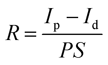
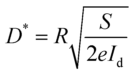
Photodetectors utilize the photoelectric effect of semiconductors to convert optical signals into electrical signals, which find extensive applications in diverse fields, such as optical communications, image capturing, and optical testing.1–6 The photoelectric effect is the phenomenon in which photons transfer their energy to the electrons of a material when they strike its surface, causing the electrons to be emitted from atoms or molecules and forming electron–hole pairs. The generation of these charge carriers (electrons and holes) leads to the current flow, thereby producing an electrical signal proportional to the intensity of the incident light.Photodetectors are characterized by several key parameters that are crucial for their performance.7 One important parameter is responsivity (R), which indicates the ability of the photodetector to convert incident light into an electrical signal. R can usually be calculated using
 | (1) |
 | (2) |
Currently, the photodetectors available on the market are mainly made of inorganic semiconductor materials, such as Si, Ge, GaAs, HgCdTe, and others.8–11 However, these materials have limitations, including their high cost and complicated fabrication process. In addition, due to band gap limitations, the photodetecting ability of these materials often only covers a specific wavelength range, with almost no optical response in the mid-to-far infrared and terahertz bands. To meet the growing demands, researchers are seeking new materials to develop photodetectors with more broad applications. Topological materials (TMs), with their unique physical properties such as non-trivial surface states, the quantum spin Hall effect,12 three-dimensional quantum Hall effect,13 zero bandgap topological structures,14 and extremely high carrier mobility, have entered the field of photodetection. These characteristics enable TMs photodetectors to surpass the performance limitations of traditional inorganic semiconductor photodetectors, particularly in wide-spectrum photodetection and low-energy consumption devices. The detection range of some TM photodetectors can even reach THz, which far exceeds the detection limit of traditional semiconductor photodetectors. As TMs continue to advance, many researchers are exploring their applications in photodetectors. However, comprehensive reviews on this emerging topic are still very limited.
This review summarizes the current research status of several widely studied TMs in photodetectors, focusing on device fabrication methods and structures. Finally, the prospects of TMs in photodetectors are discussed based on the current development status.
2 Topological materials
TMs possess topological properties, with non-linear topological invariants in the bandgap region of their electronic structure. In TMs, the behavior of electrons is constrained and guided by spatial topology, giving rise to a range of unique physical phenomena and properties.15–17 The electronic band structure of TMs is a crucial feature. For example, the energy ordering of the conduction and valence bands in regular insulator materials can be inverted by strong spin–orbit coupling (SOC), forming topological insulators (TIs).18,19 In the case of TIs, as the strength of SOC gradually decreases, the bulk energy gap reduces until it reaches zero and then gradually increases. At the phase transition point, the conduction band minimum and valence band maximum intersect simultaneously in momentum space,20 known as a topological semimetal (TSM)21–23 (Fig. 1). Compared to ordinary materials, the band structure of TMs contains unconventional levels, such as band inversions, Dirac points, Weyl points, and so on. The presence of these unconventional levels is closely related to the topological invariants, resulting in unconventional physical properties. For example, the surface states of some TMs exhibit strong topological protection, making them highly stable against external disturbances and holding significant value for applications.24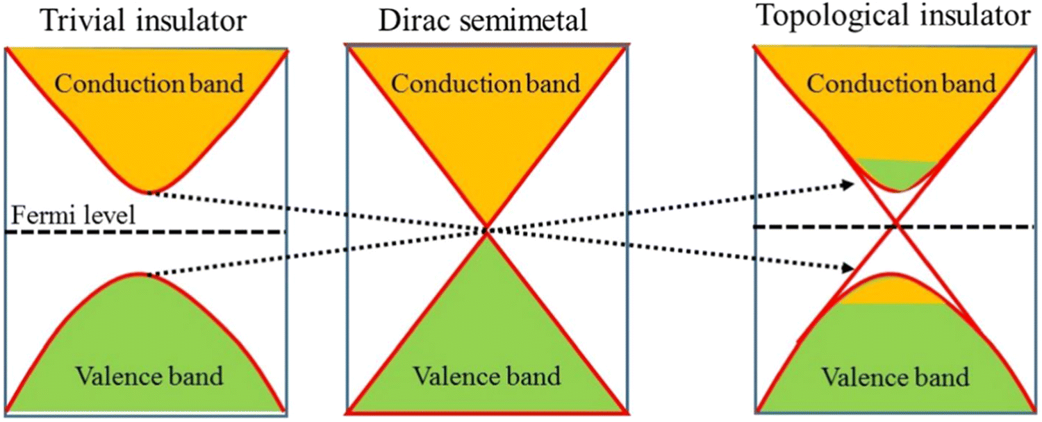 | ||
| Fig. 1 The topological insulator (TI) and Dirac semimetal (DSM). Reprinted with permission from ref. 27. Copyright 2020, Springer Link. | ||
TIs are unique materials that exhibit bulk insulating properties while conducting on their surfaces. Within a TIs, an electronic energy gap exists similar to that of a semiconductor. However, unlike semiconductors, TIs possess unique electronic states on their surfaces or edges. These particular surface states confine electrons to moving only along the material's surface or edge without penetrating the interior.25,26 The surface states of TIs are safeguarded by time-reversal symmetry and spin-momentum locking, leading to enhanced carrier mobility and reduced energy losses. This feature makes TIs suitable for photodetectors, in which low power consumption and high response times are crucial factors. The highly unique electronic properties of the topologically protected boundary states make TIs promising in the energy sector in the future.
TSMs can be classified as Dirac semimetals (DSMs) and Weyl semimetals (WSMs).28 In particular, this semimetal is a DSM if the conduction and valence bands meet at a single point and behave like massless Dirac fermions. When DSMs break the time or crystal symmetry, the corresponding Dirac fermion splits into two Weyl fermions29 of opposite chirality, thus transforming into WSMs.30–33 TSMs exhibit various exciting properties, such as extremely high carrier mobility, peculiar magnetic transport characteristics, and chiral edge modes.32 Due to the linear dispersion and spin (pseudo-spin) momentum locking, low-energy electrons in TSMs exhibit strong robustness against crystal disorder and defects, resulting in very high electron mobility.34,35 TSMs also exhibit significantly enhanced optical and photoelectric properties, such as the generation of large photocurrents,36–39 second-harmonic generation,40,41 optical activity, and gyrotopy.42,43
It is worth noting that the distinction between TIs and TSMs is not always straightforward, as some materials can exhibit characteristics of both.44 For example, some TIs may exhibit metallic behavior in their surface states, while others may have a small but finite bandgap, making them similar to TSMs. The research on TMs is still rapidly evolving, and it is interesting to see what new materials and phenomena will be discovered in the coming years.
3. Photodetectors based on topological materials
The research of TM-based photodetectors has been an active field in recent years. The distinctive electronic band structure and topological properties of TMs have introduced entirely new possibilities for optoelectronic detection technology. Compared to traditional materials, TMs exhibit an array of unique characteristics, providing them with pronounced advantages in various specialized application domains. For instance, conventional photodetectors face limitations regarding high-speed response, low noise levels, and quantum effects. TM photodetectors achieve ultrahigh charge carrier mobility thanks to their specialized electron structure. As a result, they demonstrate considerable potential in high-speed detection. This attribute offers solutions for high-speed signal detection in fields such as optical communication and radar systems. Moreover, the distinctive distribution of electron states in TMs grants them exceptional low-noise properties, giving them an advantage in weak signal detection and precision measurement applications. In domains such as astronomical observation and biomedical imaging, TM photodetectors promise to achieve higher signal-to-noise ratios and more accurate measurements. TM photodetectors exhibit broad spectral absorption properties, enabling efficient photoelectric conversion across multiple wavelength ranges. This versatility makes them suitable for various applications, including spectroscopic analysis and imaging. Additionally, certain TMs display improved sensitivity to environmental changes. This feature opens up new possibilities in environmental monitoring, chemical sensing, and related fields.Currently, TM photodetectors are mainly divided into two categories: TIs-based photodetectors, such as Bi2Se3-based photodetectors, and TSMs-based photodetectors, such as Cd3As2-based photodetectors. The preparation methods for TMs are diverse. Currently, standard fabrication methods are generally classified into bottom-up and top-down approaches. The bottom-up approaches mainly include van der Waals epitaxy, physical vapor deposition (PVD), chemical vapor deposition (CVD), molecular beam epitaxy (MBE), and pulsed laser deposition (PLD). The top-down approaches mainly include mechanical exfoliation and liquid-phase exfoliation. Each method has its advantages and disadvantages, leading to variations in the performance of the prepared photodetectors.45 Also, two-dimensional (2D) forms of TMs have unique optical and electrical properties that make them uniquely advantageous in photodetection. For example, 2D TMs have a high surface electron density and strong interlayer resonance, which leads to strong optical absorption and efficient photoelectric conversion efficiency. In addition, 2D TMs have good optical linear and non-linear properties, which make them effective as optical detectors. In addition, the thin-film form of 2D TMs is easy to prepare and package, allowing for low-cost and high-efficiency photodetection. Therefore, many researchers have focused on 2D TMs for their photodetection properties.46 Moreover, the construction of heterostructure can enhance the photodetecting performance of photodetectors. Consequently, many researchers have explored the photoelectric properties of heterostructures that combine TMs.
The research on TM photodetectors has achieved considerable results, for example, a significant improvement in photodetection efficiency, response speed, responsivity, etc. However, several challenges remain, such as growth quality control and stability issues. Therefore, there is still plenty of room for research on TM photodetectors.
3.1 Topological insulator photodetectors
The primary reason for the attention and development of TIs in photodetectors is their distinctive electronic structure. The topological surface states of these materials, constrained by both spin-coupling effects and time-reversal symmetry, exhibit small energy losses and high charge mobility. This makes them an ideal choice for developing low-power, high-response-rate electronic and optoelectronic devices.In the photodetector domain, TIs primarily include Bi2Se3, Bi2Te3, Sb2Te3, and SnTe. Hence, this section will be centered around these core materials, providing a comprehensive summary of the research progress. Among these materials, Bi2Se3 is the pioneer to enter the field of photodetecting owing to its unique properties, such as high carrier mobility and a narrow 0.3 eV band gap. Bi2Se3 is a typical TI layered material with spin-locked Dirac cones in the outer layer and insulating band gaps in the inner layer. Observing along the c-axis (Fig. 2a),47 the crystal structure of Bi2Se3 can be described as a layered compound composed of five atomic layers arranged in a repeating pattern. The stacking order is Se1–Bi–Se2–Bi–Se1, where “1” and “2” represent two distinct chemical states of the selenium anion.
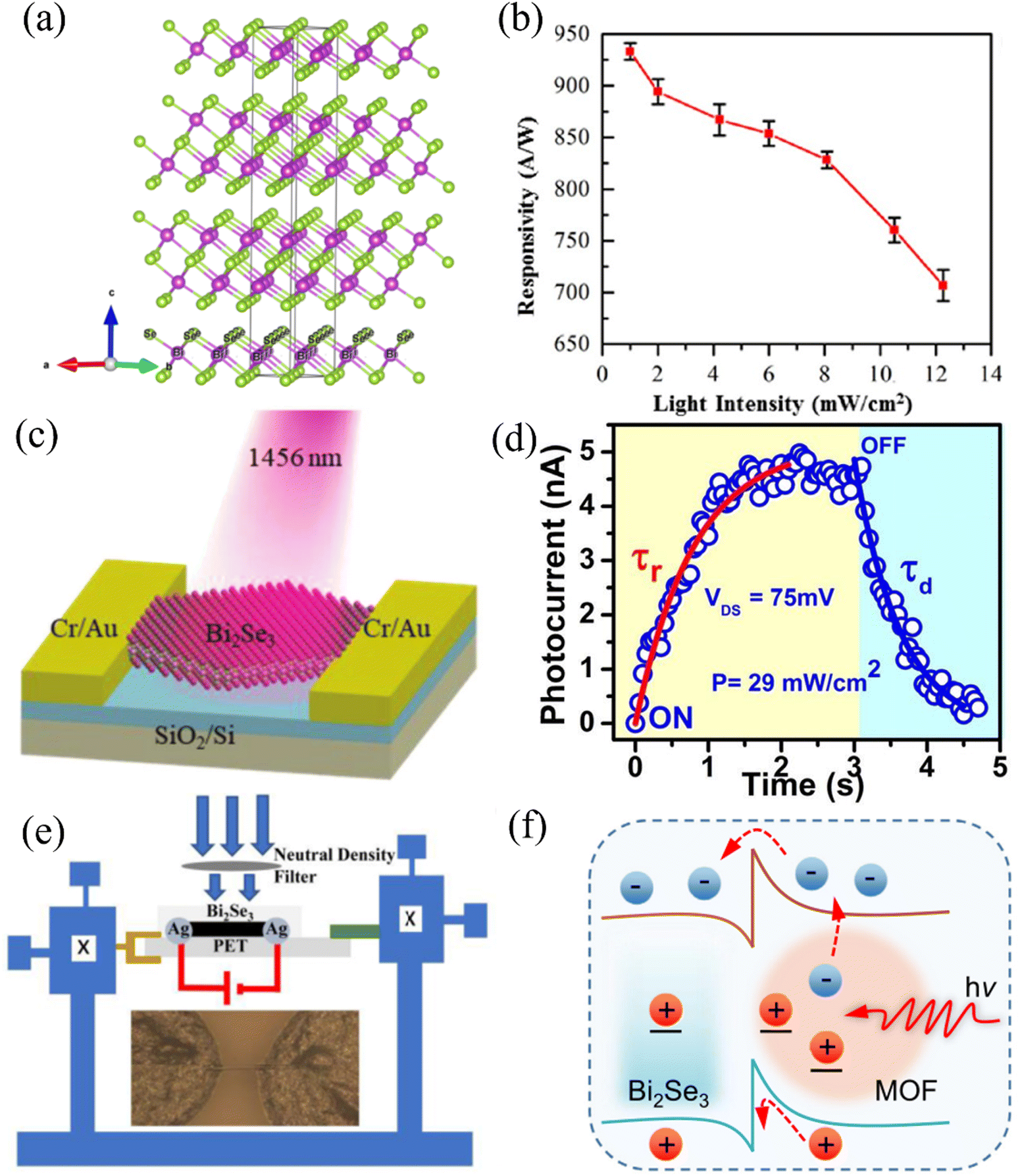 | ||
| Fig. 2 (a) The schematic depiction showcases the crystal structures of Bi2Se3, where weak van der Waals interaction connects the quintuple layers. In the illustration, purple represents Bi atoms, while green represents Se atoms. Reprinted with permission from ref. 47. Copyright 2021, Elsevier. (b) Responsivities of Bi2Se3/Si nanowire near-infrared photodetector under different NIR intensities. Reprinted with permission from ref. 48. Copyright 2017, American Chemical Society. (c) Bi2Se3 photodetector on Si/SiO2 substrate. Reprinted with permission from ref. 49. Copyright 2018, Wiley. (d) The response and decay times of the Bi2Se3 nanowire device. Reprinted with permission from ref. 50. Copyright 2014, Nature. (e) The experimental arrangement used to investigate the strain modulation effect in Bi2Se3 NWs. The inset within the figure displays an optical microscope image of the PD. Reprinted with permission from ref. 51. Copyright 2019, Elsevier. (f) Schematic band diagram of the Bi2Se3/MOF hybrid heterojunction under illumination. Reprinted with permission from ref. 52. Copyright 2022, Springer Nature. | ||
Biswajit Das et al.48 have prepared a Bi2Se3 nanosheet/Si nanowire heterojunction near-infrared detector using green, environmentally friendly, and cost-effective chemical technology. Fig. 2b shows the variation of R with light intensity in Bi2Se3 heterojunction devices. The maximum R and D* are 934.1 A W−1 and 2.30 × 10¹³ Jones (at ±0.5 V). Wang et al.49 successfully prepared Bi2Se3 thin films using van der Waals epitaxy (VDWE) on graphene and investigated the optical properties of photoconductive detectors based on these thin films. As shown in Fig. 2c, under the illumination of 1456 nm light, the switching ratio, R, and external quantum efficiency (EQE) are as high as 972.5, 23.8 A W−1 (at 1.0 V), and 2035%, respectively. Although the R is lower than that of the nano-heterojunction device,48 its detection range is larger. The research on Bi2Se3 thin film devices for photodetecting has been successful, and the study of its nanowire devices in photodetecting has also garnered much attention. Sharma et al.50 obtained nanowires (NWs) by micromechanical exfoliation (ME) of the Bi2Se3 film, followed by further processing using a focused ion beam (FIB). The fabricated NW device shown in Fig. 2d exhibited photoelectric response across the visible to infrared light range. Under 1064 nm light, the Bi2Se3 nanowire device had a R up to 300 A W−1 at a bias voltage of 0.075 V, with a rapid rise/decay in response time and good photocurrent repeatability. In addition to the influence of preparation methods on the photodetecting performance of devices, the performance of the devices can also be controlled through defects, applied strain, and doping. Wang et al.51 utilized CVD to fabricate Bi2Se3 NWs. The device exhibited a R of 191.75 mA W−1 and a D* of 6.6 × 10¹⁰ Jones under 442 nm illumination at the bias voltage of 2.0 V. They observed that upon introducing external compressive strain (Fig. 2e), the Ip and R of the device increased by 97% and 503%, respectively. According to their study, the strain modulation effect under compressive strain reduces the Schottky barrier height (SBH) and junction resistance, facilitating the transfer of photoexcited charge carriers and enhancing the photodetecting performance of the device. Therefore, strain modulation of nanoscale photodetectors through applied strain is a promising direction for future development. In another study, Zhai et al.52 prepared a Bi2Se3/MOF heterojunction thin film high-performance infrared photodetector by hybridizing MOF with Bi2Se3 sheets. The MOF serves a dual role in the system. First, it functions as a photosensitive material, absorbing incident light. Additionally, it acts as a photogate layer, allowing it to control the conductance of the Bi2Se3 channel (Fig. 2f). The strong light absorption of MOF and the high carrier mobility of 2D Bi2Se3 sheets led to excellent photo response performance in the 500–2000 nm wavelength range. The R and D* at 1500 nm found to be 4725 A W−1 and 3.5 × 10¹³ Jones at the bias voltage of 1.0 V, respectively, two to three orders of magnitude higher than those of the original Bi2Se3-based photodetectors. These studies have demonstrated the significant potential of Bi2Se3-based material for high-performance photodetectors. These findings indicate that Bi2Se3 heterojunction photodetectors show significant improvements in terms of R and D* compared to previous single Bi2Se3 photodetectors.
Bi2Te3 is also a famous TM with high carrier mobility and a narrow band gap,59 which has a broad development prospect in photodetection. Bi2Te3 is a well-studied thermoelectric material.60–62 It was not until recently, though, that its photodetecting capabilities were noticed. Like Bi2Se3, Bi2Te3 also has a layered structure bound by van der Waals forces, with five layers of atoms arranged along the c-axis and periodically stacked (Fig. 3a). Compared with Bi2Se3, Bi2Te3 has a smaller bulk band gap of 0.17 eV. Fig. 3b shows the energy band of Bi2Te3. Therefore, Bi2Te3 has attracted extensive attention in the field of long-wavelength photodetection. Liu et al.54 fabricated single-crystal Bi2Te3 photodetectors on silicon by MBE, which showed a response from 1064–1550 nm. When the laser wavelength is 1550 nm, the R and internal quantum efficiency are 3.32 × 10⁻² A W−1 and 7.4% at a bias voltage of 1.0 V, respectively. Under the irradiation of 1064 nm light, the R and internal quantum efficiency are 3.64 × 10⁻³ A W−1 and 0.9%, respectively.
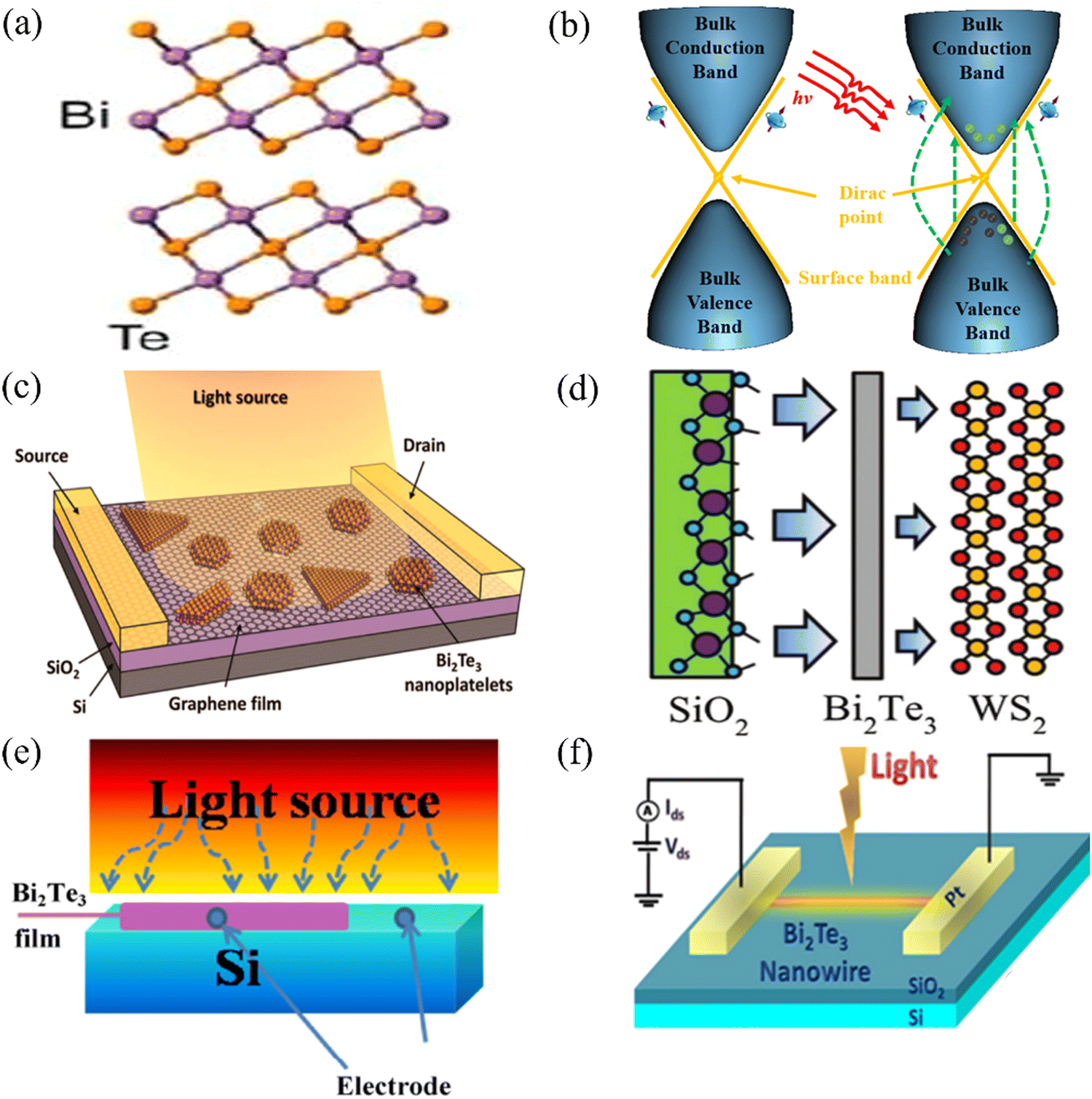 | ||
| Fig. 3 (a) Schematic illustration of the Bi2Te3 crystal structures. Reprinted with permission from ref. 53. Copyright 2022, American Chemical Society. (b) Optical transition channels between Bi2Te3 bands. Reprinted with permission from ref. 54. Copyright 2017, Amer Inst Physcis. (c) Schematic of the graphene/Bi2Te3 heterostructure phototransistor device. Reprinted with permission from ref. 55. Copyright 2015, American Chemical Society. (d) The operational principle underlying the WS2/Bi2Te3 photodetectors. Reprinted with permission from ref. 56. Copyright 2016, Royal Society of Chemistry. (e) Schematic of the n-Bi2Te3/p-Si junction structure. Reprinted with permission from ref. 57. Copyright 2017, Springer Nature. (f) Represents the schematics used for the photoelectric characterization. Reprinted with permission from ref. 58. Copyright 2017, American Chemical Society. | ||
Heterojunction devices composed of Bi2Te3 and other materials also exhibit good photoelectric properties. Qiao et al.55 prepared a graphene/Bi2Te3 heterojunction-efficient photodetector by combining the ultrafine and broadband photoresponse properties of graphene with the excellent properties of Bi2Te3 in photodetecting (Fig. 3c). The device's R at 532 nm can reach 35 A W−1 at the bias voltage of 1.0 V, and the photoconductance gain is up to 83. Yao et al.56 prepared a WS2/Bi2Te3 heterojunction photodetector to study the photodetecting performance of WS2. As shown in Fig. 3d, the Bi2Te3 layer acts as a passivation layer. It shields the interference of SiO2 on WS2. Consequently, the device achieves an optical response range of 370–1550 nm with an R of 30.7 A W−1 and a D* of 2.3 × 10¹¹ Jones at the bias voltage of 4.0 V. Wang et al.57 prepared n-type Bi2Te3 films on p-type Si substrates by CVD (Fig. 3e). This heterojunction device showed good photoelectric properties. The material demonstrates a strong photovoltaic effect across a broad spectrum, from ultraviolet (UV) to near-infrared (NIR) wavelengths. Remarkably, it attained a short-circuit current of 19.2 μA and an open-circuit voltage of 235 mV when subjected to a 1000 nm wavelength. Additionally, the material exhibited rapid response times of only a few milliseconds. Yao et al.63 prepared Bi2Te3–SnSe–Bi2Te3 photodetectors by combining 2D Bi2Te3 and SnSe. Because the energy band between Bi2Te3 and SnSe can be perfectly matched, the device has a good optical response in the range of UV to NIR (370–808 nm). After optimization, the R is 5.5 A W−1, and the D* is 6 × 10¹⁰ Jones at a bias voltage of 20.0 V. Sharma et al.58 further investigated the photoelectric properties of Bi2Te3 NWs devices (Fig. 3f). They fabricated nanowire devices by FIB milling. Under near-infrared laser irradiation, the optical R of the NWs device is 780 A W−1 and D* is 1.2 × 10⁹ Jones at the bias voltage of 0.3 V. In addition, Sharma et al. also confirmed that the photodetecting performance of the device was hardly affected after 4 months in ambient conditions, which showed the superior stability of the Bi2Te3 NWs device.
Unlike other TIs, SnTe has a highly symmetrical crystal structure thus called a topological crystal insulator (TCI).68 There is evidence that mirror symmetry protects the singular surface states of topological crystal insulators.69,70 In addition, compared with other TMs, SnTe is easier to synthesize. These unique properties make SnTe a good research prospect in photodetection. In 2017, Gu et al.64 prepared SnTe/Si photovoltaic detectors (Fig. 4a) by CVD for the first time. The detector can realize light response in the wide spectral range of 254–1550 nm. Under 808 nm laser irradiation, the device exhibited the best light response, with a D* of 8.4 × 10¹² Jones and a switching ratio of 5 × 10⁶ at a bias voltage of 0 V. Moreover, it has a fast response time, with a rise time of 8 μs and a fall time of 0.39 ms. However, this device requires high light intensity, and the light intensity significantly affects the photocurrent. Jiang et al.65 fabricated the inaugural SnTe thin-film photodetector by MBE (Fig. 4b). The photodetector has a wide spectral response ranging from 405 nm–3.8 μm, with a R of 3.75 A W−1 at 2003 nm at a bias voltage of 2.0 V. Yang et al.66 fabricated SnTe nanocrystal photodetectors directly on polyethylene terephthalate (PET) films in 2018 (Fig. 4c). The device has a broad spectral response (254–4650 nm). The R can reach 71.11 A W−1 under 254 nm at a bias voltage of 1 V. This detector can also exhibit the same light response on the flexible substrate. Therefore, it is expected to be well-developed in wearable devices. In 2022, Song et al.67 prepared heterogeneous structures of SnTe and Ge using magnetron sputtering technology (Fig. 4d). The detector exhibits diode and photovoltaic characteristics in the visible to NIR band (400–2050 nm). Under 850 nm NIR illumination, the R and D* of the photodetector reached a value of 0.62 A W−1 and 2.33 × 10¹¹ Jones at a bias voltage of −0.5 V, respectively.
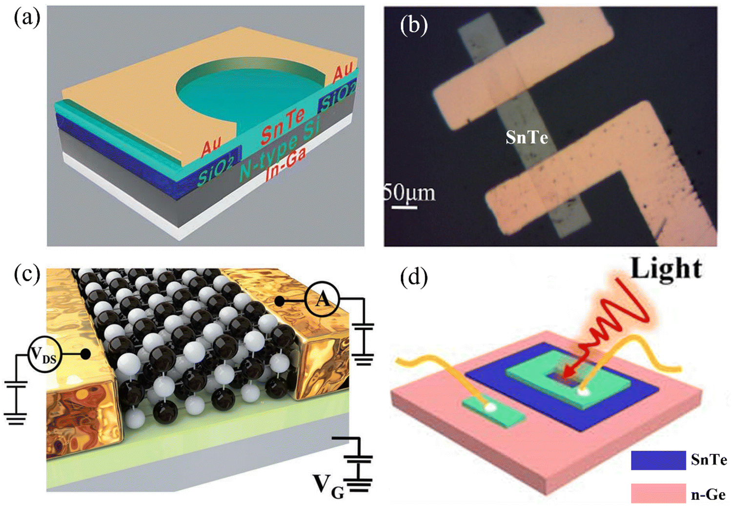 | ||
| Fig. 4 (a) Photovoltaic detectors based on a heterostructure of SnTe/Si. Reprinted with permission from ref. 64. Copyright 2017, Royal Society of Chemistry. (b) OM image of the SnTe thin-film photodetector. Reprinted with permission from ref. 65. Copyright 2017, Wiley. (c) Schematic of the SnTe-based photodetector. Reprinted with permission from ref. 66. Copyright 2018, Wiley. (d) SnTe/n-Ge photovoltaic detector. Reprinted with permission from ref. 67. Copyright 2022, Institute of Physics Publishing. | ||
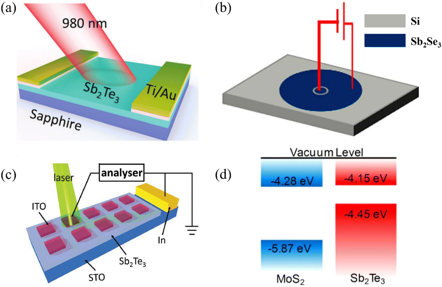
Sb2Te3 is also a typical TI. The band gap of Sb2Te3 is only 0.3 eV, and its carrier concentration and mobility are very high, at 1019–1020 cm−3 and 200 cm2 V−1 s−1, respectively.75 Because of these characteristics, Sb2Te3 has broad applications in photodetection. In 2015, Zheng et al.71 studied the related performance of Sb2Te3 thin-film photodetectors (Fig. 5a). They successfully fabricated thin-film photodetectors through MBE. The bias voltage is set to be 1 V under 980 nm light, the R is 21.7 A W−1, the photoconductance gain is 27.4, and the switching ratio is 2.36. 2D p–n heterostructures are an essential research direction in integrated electronics and optoelectronics due to their unique physical, optical, and electrical properties.76 Sb2Te3 is a p-type semiconductor, and finding a suitable n-type material in combination with Sb2Te3 could improve its photoelectric response. Si is an easily obtained n-type semiconductor, Yu et al.72 fabricated a broadband self-powered photodetector based on Sb2Te3 and Si using photolithography and thermal evaporation technology. This detector has a fast response speed (<40 ms) and can realize photodetecting at 365–940 nm. By setting up an asymmetrical electrode structure, as shown in Fig. 5b, the detector can be self-powered for a broader range of applications. Zhang et al.77 also prepared the Sb2Te3/n-Si heterojunction. They adopted the magnetron sputtering technology because of its lower cost and easier operation. After annealing, the detector can achieve a broad spectral response of 250–2400 nm, and the R and D* can reach 270 A W−1 and 1.28 × 10¹³ Jones at 2400 nm at a bias voltage of 0.5 V. These performances are better than those of other reports, probably because annealing changes the crystallinity of the thin film. Sun et al.73 prepared Sb2Te3 thin films on n-type SrTiO3 (STO) substrates using MBE to constitute p–n heterojunction photodetectors (Fig. 5c). The detector can detect a wide spectrum from 405–1550 nm, and the switching ratio of the heterojunction device is 1.58 × 10⁶ at 405 nm. Also, the rise time is only 30 μs, and the fall time is 95 μs, faster than most other TI photodetectors. Liu et al.74 successfully synthesized vertically stacked Sb2Te3/MoS2 heterostructures by van der Waals epitaxial growth using the n-type material MoS2. As shown in Fig. 5d, Sb2Te3/MoS2 forms a type-II band alignment at the interface. The type-II band alignment effectively separates photoexcited charge carriers, enhancing the device's performance. Due to the distinctive band structure of the type-II band alignment heterojunction, it enables wide-band photoelectric response. This heterojunction has excellent photodetecting performance, with up to 106 ultra-high current rectification rates and 4.5% photoelectric conversion efficiency. The R reaches 330 A W−1 by applying a negative voltage bias (−1 V) on the drain electrode, and the D* is 1012 Jones. This is one of the highest values of TI p–n junction photodetectors.
 | ||
| Fig. 5 (a) The schematic illustration of the Sb2Te3 film photodetector. Reprinted with permission from ref. 71. Copyright 2015, Royal Society of Chemistry. (b) Schematic representation of Sb2Te3 electrodes on a silicon substrate. Reprinted with permission from ref. 72. Copyright 2019, Institute of Physics Publishing. (c) The schematic diagram of the Sb2Te3 array photodetector and the measurement setup. Reprinted with permission from ref. 73. Copyright 2017, Royal Society of Chemistry. (d) Band structures of the achieved Sb2Te3/MoS2 heterostructures. Reprinted with permission from ref. 74. Copyright 2019, Elsevier. | ||
In addition to the aforementioned binary photodetectors, Bi2Te2Se and Sb2SeTe2 and other ternary TMs have also entered the research scope. However, it is still in its infant stage. A few photodetectors with ternary topologies have been reported. In 2017, Huang et al.78 studied the photodetecting performance of the Sb2SeTe2 nanoflake. In this study, Sb2SeTe2 showed remarkable performance. Under 532 nm wavelength illumination and a 1 V bias voltage, the R and photoconductance gains reached 2293 A W−1 and 5344, respectively. This is several orders of magnitude more responsive than previously reported TI photodetectors, suggesting that Sb2SeTe2 has great potential in the field of photodetectors. In 2021, G. K. Maurya et al.79 integrated Bi2Te2Se films and a silicon substrate to form a transverse heterojunction photodetector. Studies have shown that the Bi2Te2Se/Si heterojunction has a good photoelectric response in the range of visible light to near-infrared, and under 900 nm light, the R is 19.06 A W−1 under positive bias (+2 V), the D* is 8 × 10¹¹ Jones. The R is 12.64 A W−1 under reverse bias (−2 V), and the D* is 7.72 × 10¹¹ Jones. Bi2Te2Se has now also been found to have promising applications in THz detection.80
Table 1 summarizes the key parameters and preparation methods of TI photodetectors in recent years. It can be seen that the long wave detection limit of TI photodetectors is approximately 5 μm away from the NIR band. Thin film and nanowire devices typically have better photodetecting performance owing to the advantages of nanoscale materials. In addition, the preparation method also has a significant impact on the photodetecting performance. For example, the R of Bi2Se3 NW prepared by ME is three orders of magnitude higher than that prepared by CVD. Therefore, optimized nanostructures and preparation processes are crucial to improving photodetecting performances.
| Material | Synthesis method | Responsivity (A W−1) | Detectivity (Jones) | Detection range (nm) | Ref. |
|---|---|---|---|---|---|
| Bi2Se3 NS/Si | — | 9.34 × 10² | 2.30 × 10¹³ | NIR | 48 |
| Bi2Se3 film | VDWE | 23.8 | — | 1456 | 49 |
| Bi2Se3 NW | ME | 3 × 10² | — | Visible-infrared | 50 |
| Bi2Se3 NW | CVD | 1.92 × 10⁻¹ | 6.6 × 10¹⁰ | 325–1064 | 51 |
| Bi2Se3/MOF | — | 4.725 × 10³ | 3.5 × 10¹³ | 500–2000 | 47 |
| Bi2Te3 | MBE | 3.32 × 10⁻² | — | 1064–1550 | 54 |
| Graphene/Bi2Te3 | — | 0.35 × 10² | 83 | UV-NIR | 55 |
| WS2/Bi2Te3 | — | 0.307 × 10² | 2.3 × 10¹¹ | 370–1550 | 56 |
| Bi2Te3/Si | CVD | — | — | UV-NIR | 57 |
| Bi2Te3/SnSe/Bi2Te3 | — | 5.5 | 6 × 10¹⁰ | 370–808 | 63 |
| Bi2Te3 NW | FIB | 7.8 × 10² | — | NIR | 58 |
| SnTe/Si | CVD | — | 8.4 × 10¹² | 254–1550 | 64 |
| SnTe film | MBE | 3.75 | — | 405–3.8 μm | 65 |
| SnTe/PET | — | 0.71 × 10² | — | 254–4650 | 66 |
| SnTe/Ge | PVD | 0.62 | 2.33 × 10¹¹ | 400–2050 | 67 |
| Sb2Te3 film | MBE | 0.22 × 10² | 1.22 × 10¹¹ | NIR | 71 |
| Sb2Te3/Si | PEP | — | — | 365–940 | 72 |
| Sb2Te3/Si | PVD | 2.7 × 10² | 1.28 × 10¹³ | 250–2400 | 77 |
| Sb2Te3/STO | MBE | 4.8 × 10⁻³ | 8.6 × 10¹⁰ | 405–1550 | 73 |
| Sb2Te3/MoS2 | CVD | 3.3 × 10² | 1012 | — | 74 |
| Sb2SeTe2 nanoflake | — | 2.29 × 10³ | 4.5 × 10⁸ | 532 | 78 |
| Bi2Te2Se/Si | — | 0.19 × 10² | 8 × 10¹¹ | Visible-infrared | 79 |
In photodetector application and development, the unique electronic structure of TIs gives them significant competitive edges compared to conventional materials. TIs demonstrate notably low energy losses and high charge mobility, laying a robust foundation for developing high-performance photodetectors. Additionally, the bandgap of TIs plays a crucial role in mitigating carrier recombination, further enhancing the sensitivity and response speed of detectors. Nevertheless, certain traditional materials may showcase superior optoelectronic performance within specific wavelength ranges. Hence, when selecting materials, it is essential to comprehensively consider the characteristics of different materials according to the specific requirements of the intended applications.
3.2 Topological semimetal photodetectors
With the progress of TMs, more TMs in the photodetecting field. In addition to the TIs discussed above, TSMs have gained attention recently. TSMs display a linear energy dispersion in their bulk state, where the conduction and valence bands intersect at topologically protected Dirac or Weyl nodes.81 TSMs have many attractive physical properties, such as ultra-high electron mobility,82 zero band gap, a topological Fermi arc, and the quantum Hall effect.83–85 These physical properties extend the detectable spectral range of TSMs even to THz.86 Cd3As2, PtSe2, PtTe2, MoTe2 and TaIrTe4 are the most studied TSMs. Other materials, such as WTe2 and TaAs, also appear promising, even in their initial stages of research.To date, the study of topological DSM photodetectors has mainly focused on Cd3As2. Cd3As2 is one of the first identified TSMs,87 with a centrally symmetric tetragonal crystal structure.88 Electronic structure calculations show that Cd3As2 is a 3D electronic analog of 3D DSM and graphene without spin splitting.89 As early as 2013, Wang et al.90 demonstrated through first-principle calculation and practical model analysis that Cd3As2 is a symmetrically protected TSM, paving the way for further studies. In a subsequent study, Liu et al.91 confirmed this conclusion by directly observing a pair of 3D Dirac Fermions in Cd3As2 using angle-resolved photoelectron spectroscopy. Mosca Conte et al.92 used density functional theory to study the electronic and optical properties of Cd3As2 and provided theoretical evidence for its potential use in wide-spectrum photodetecting. For their research on photodetectors, Wang et al.93 employed CVD to synthesize Cd3As2 NWs and nanoplate devices. The nanoplate devices exhibited enhanced photoelectric response characterized by relatively low resistance and high carrier mobility. With a R of 5.9 mA W−1, it was shown that the response capabilities could span the wavelength range of 532 nm to 10.6 μm. These findings highlight the promising potential of Cd3As2 in photodetector components. Compared to submicron-structured photodetectors, their thin-film-based counterparts typically offer a higher photocurrent response owing to their larger photosensitive area, affording more pronounced detection advantages. In 2021, Yao et al.94 employed the MBE technique to fabricate Cd3As2 thin films, extending the Cd3As2 photodetecting range into the THz frequency regime. They successfully realized room-temperature detection of THz waves utilizing Cd3As2, exhibiting high sensitivity, low energy requirements, and rapid response characteristics.
However, semimetal has an intrinsic ultra-high charge transfer rate and low resistance. Thus, even a small external bias can cause significant dark current, thereby limiting the device's performance, particular switch ratio and D*. Building heterojunction photodetectors can effectively improve the photoelectric detector's performance. In 2018, Yang et al.95 reported a broadband photodetector based on a Cd3As2 thin film/pentacene heterojunction. As shown in Fig. 6c, this photodetector can detect radiation wavelengths ranging from 450–10![[thin space (1/6-em)]](https://www.rsc.org/images/entities/char_2009.gif) 600 nm at room temperature. Under illumination at 650 nm, it achieves a R of 36.15 mA W−1 at a bias of 0.5 mV. The outstanding performance of this photodetector in the long infrared wavelength range makes it promising in information communication. The combination of organic matter and thin film provides a new direction for studying Cd3As2 photodetection. Building upon this work, they substituted pentacene with small molecules and polymers,96 expanding the detection range of Cd3As2-based photodetectors to 365–10600 nm at bias zero. Moreover, the R was significantly improved to 729 mA W−1. In 2022, Yang et al.97 realized the light response from the visible to the infrared band by constructing a double heterojunction. They prepared a wideband photodetector with Cd3As2/ZnxCd1−xTe/GaSb vertical heterostructure through simple and controllable magnetron sputtering and photolithography technology. They further demonstrated its imaging application, which makes the Cd3As2 heterostructure promising for practical devices.
600 nm at room temperature. Under illumination at 650 nm, it achieves a R of 36.15 mA W−1 at a bias of 0.5 mV. The outstanding performance of this photodetector in the long infrared wavelength range makes it promising in information communication. The combination of organic matter and thin film provides a new direction for studying Cd3As2 photodetection. Building upon this work, they substituted pentacene with small molecules and polymers,96 expanding the detection range of Cd3As2-based photodetectors to 365–10600 nm at bias zero. Moreover, the R was significantly improved to 729 mA W−1. In 2022, Yang et al.97 realized the light response from the visible to the infrared band by constructing a double heterojunction. They prepared a wideband photodetector with Cd3As2/ZnxCd1−xTe/GaSb vertical heterostructure through simple and controllable magnetron sputtering and photolithography technology. They further demonstrated its imaging application, which makes the Cd3As2 heterostructure promising for practical devices.
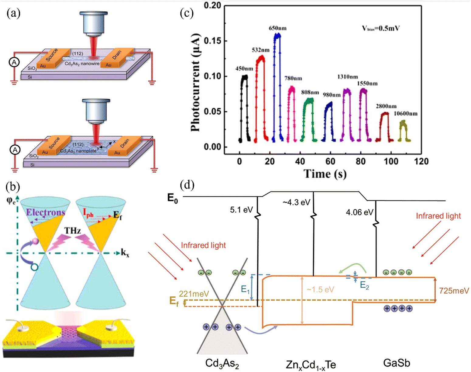 | ||
| Fig. 6 (a) The diagram illustrates the scanning photocurrent measurement setup used for Cd3As2 nanowire and nanoplate devices. Reprinted with permission from ref. 93. Copyright 2017, American Chemical Society. (b) Schematic of the Cd3As2-based THz detector and photoconduction process of THz-excited Dirac fermions. Reprinted with permission from ref. 94. Copyright 2021, American Chemical Society. (c) Photocurrent curves of the Cd3As2 thin film/pentacene heterojunction photodetector with 0.5 V bias voltage. Reprinted with permission from ref. 95. Copyright 2018, American Chemical Society. (d) Band bending diagram with zero bias. Here, E0, Ef, E1, and E2 represent the vacuum, Fermi, and the barrier heights between ZnxCd1−xTe and Cd3As2 or GaSb, respectively. The electron affinity of the three layers and the bandgaps of ZnxCd1−xTe and GaSb are also indicated. Upon illumination, the heterostructures experience photogeneration, generating electrons in GaSb and holes in Cd3As2. These photogenerated carriers migrate into the buffer layer, driven by the built-in electric field at the interfaces. The band diagram illustrates the direction of carrier movement, with the purple/green arrow indicating the direction of photogenerated holes/electrons. Reprinted with permission from ref. 97. Copyright 2022, American Chemical Society. | ||
PtTe2 is a DSM with a CdI2-type triangular (1T) structure, with six Te atoms surrounding each Pt atom.98,99 In 2018, Xu et al.100 reported a THz photodetector based on 2D PtTe2. The device can be operated in self-powered mode. At zero bias, the R is as large as 1.6 A W−1 with a response time of less than 20 μs. At a bias of −100 mV, the R can reach 3.8 A W−1. In addition, they also constructed photodetectors based on graphene/PtTe2 heterojunction, which can achieve a response time of less than 9 μs. In 2020, Tong et al.101 reported successfully fabricating large-area PtTe2 thin films through direct telluration of platinum. They developed PtTe2/Si-based near-infrared photodetectors and image sensors based on these films. As shown in Fig. 7b, the photodetector exhibited a broadband response ranging from 200–1650 nm, with a maximum R at 980 nm. Under illumination at 980 nm, the photodetector exhibited a R and D* of 0.406 A W−1 and 3.62 × 10¹² Jones, respectively, with an EQE of up to 32.1% at zero bias.
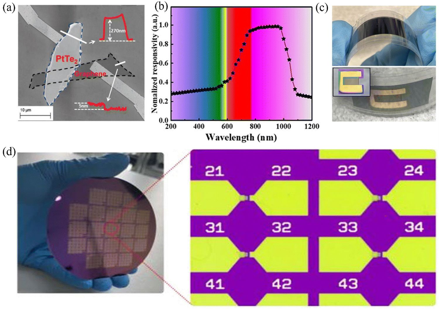 | ||
| Fig. 7 (a)The SEM diagram of the device. Reprinted with permission from ref. 100. Copyright 2019, Wiley. (b) Normalized responsivity of the PtTe2/Si NIRPD at zero bias. Reprinted with permission from ref. 101. Copyright 2022, American Chemical Society. (c) The top image showcases a thin Si wafer subjected to bending, while the bottom image displays a flexible 2D PtTe2/Si photodetector. Reprinted with permission from ref. 102. Copyright 2021, American Chemical Society. (d) Large-scale PtTe2/graphene photodetectors on a 4-in. wafer. Reprinted with permission from ref. 103. Copyright 2022, American Chemical Society. | ||
Additionally, it demonstrated a very high response speed, with a rise time of only 7.51 μs and a fall time of 36.7 μs. The PtTe2-based image sensor also exhibited excellent performance in infrared imaging. Wearable photodetectors have significant potential for diverse applications in imaging, sensing, optical communication, and environmental monitoring as photodetecting technology advances in the Internet of Things era.104 Similar to the work of Tong, Shawkat et al.102 directly fabricated a 2D PtTe2 layer on a thin silicon wafer (Fig. 7c), enabling the fabrication of flexible 2D PtTe2 photodetectors in the spectral range of 1–7 μm. This flexible detector demonstrated excellent photodetecting performance through extensive bending experiments, validating its potential for use in wearable photodetectors. This work significantly broadens the multifunctionality of Si-based photodetectors. In 2022, Yu et al.103 successfully fabricated highly controllable wafer-scale PtTe2/graphene 2D Dirac heterostructure photodetectors using CVD and photolithography techniques. The thickness and size of the devices can be adjusted, and they are compatible with complementary metal–oxide–semiconductor (CMOS) technology (Fig. 7d). This fabrication method holds practical significance in integrated multifunctional photodetectors. The R of the photodetector can reach 0.52 A W−1 without bias, and D* can reach 2.58 × 10¹⁰ Jones.
PtSe2 is a class DSM,105 widely studied in photodetecting. Yu et al.106 synthesized PtSe2 by chemical vapor phase transport (CVT) and then prepared 2D PtSe2 photodetectors by mechanical exfoliation. They found that the bilayer PtSe2 devices were suitable for broadband mid-infrared photodetectors. The broadband range extends from visible to mid-infrared, with fast response and high sensitivity. In 2020, Feng et al.107 studied the photoelectric properties of PtSe2 and perovskite CsPbX3 (X = Cl, Br, I) heterostructures. It showed through first-principle calculations that such heterostructures could improve the photoelectric carrier separation ability, broaden the absorption spectrum, and improve their photodetecting ability. Yang et al.108 employed few-layer PtSe2 to fabricate photodetector devices, with the primary mechanism for photocurrent generation being the photogating effect. This device exhibited an extremely high photoresponsivity and photocurrent, reaching a R of 5 × 10⁴ A W−1 at a bias voltage of 0.2 V. Moreover, they showed that the gate voltage can determine whether the device exhibits positive or negative photoconductance. Like PtTe2 mentioned earlier, PtSe2 can also be produced on a large scale through the direct sulfurization of Pt. Zeng et al.109 utilized this method to construct a PtSe2/Si NW. This device exhibited a R of 12.65 A W−1 at a bias voltage of −5 V, a D* of 2.5 × 10¹³ Jones, and an exceptionally high response speed. This array photodetector holds significant potential for future applications in optoelectronic and electronic devices.
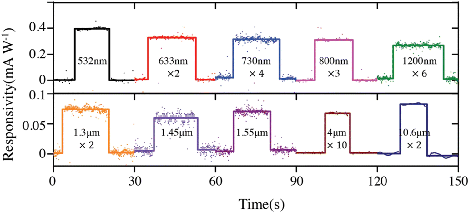
Owing to its unique material properties, the WSM photodetector has an excellent sensitivity, broadband range, and self-powered operation performance. MoTe2 is considered to be a possible WSM. Typically, MoTe2 has three crystal structures: 2H, 1T′, and Td phases, in which 1T′ and 2H phases are trivial, Td phase is non-trivial.111,112 Lai et al.110 prepared a Td-MoTe2 broadband self-powered photodetector based on WSM's special unique material properties. The detector can not only achieve a broadband response of 532–10600 nm (Fig. 8). Under 532 nm light irradiation, the device's R can reach 0.40 mA W−1, the D* is 1.07 × 10⁸ Jones at zero bias voltage, and the response time is 43 μs. However, despite the potential of WSMs in broadband photodetection, achieving large-scale synthesis for flexible devices remains a challenge. Notably, a significant breakthrough has recently been achieved in this regard. Through MBE techniques, Yang et al.113 successfully grew centimeter-scale Td-MoTe2 films on flexible mica substrates. This result has introduced fresh possibilities for the application of MoTe2 in the field of photodetection. It is worth emphasizing that the antenna-less, self-powered flexible photodetectors based on Td-MoTe2 exhibit outstanding performance. At room temperature, these detectors demonstrate remarkable electromagnetic radiation detection capabilities from ultraviolet to sub-millimeter wave regions and a rapid response time of approximately 20 microseconds. More notably, the detector's responsivity reaches 0.53 mA W−1 (2.52 THz), with a NEP of 2.65 nW Hz−0.5 (2.52 THz). These remarkable performance characteristics set MoTe2 materials apart in photodetection, establishing a solid foundation for their application in wearable technology and other related domains.
 | ||
| Fig. 8 Photocurrent response of the MoTe2 device at different excitation wavelengths. Reprinted with permission from ref. 110. Copyright 2018, Wiley. | ||
Polarization-sensitive photodetecting has attracted much attention because of its unique applications. WSM also has a good development prospect in polarization-sensitive photodetecting. For example, the MoTe2 broad spectrum self-powered photodetector110 mentioned earlier also has an anisotropic response sensitive to the polarization angle. It exhibits an anisotropic response in the 532–10600 nm range, with an anisotropic ellipse ratio up to 2.72 in the 10600 nm band. Nevertheless, the intrinsic in-plane symmetry of the materials and the single structure of the detector impede the advancement of polarization detectors with high anisotropy ratios. TaIrTe4 is a type-II WSM with an orthogonal structure and strong in-plane asymmetry. Therefore, TaIrTe4 has attracted extensive attention in developing polarization-sensitive photodetectors. In 2018, Lai et al.114 took the lead in constructing a photodetector based on TaIrTe4, which could achieve a photoelectric response of 532–10600 nm. Under the irradiation of 10.6 μm light, the R is 20 μA W−1, and the D* is 1.8 × 10⁶ Jones at zero bias voltage. In addition, they demonstrated the anisotropic response of the TaIrTe4 photodetector with polarized light. Its anisotropy ratios are 1.13, 1.56, and 1.88 at 633 nm, 4 μm, and 10.6 μm, respectively. It is not difficult to see that as the wavelength increases, the anisotropy becomes stronger. Han et al.115 further constructed a WSe2/TaIrTe4/MoS2 heterojunction photodetector in 2021. This heterojunction photodetector could achieve a wide spectral photoelectric response ranging from 405–1550 nm. At 635 nm wavelength, the device has a R of 1.48 A W−1 and a D* of 1011 Jones at zero bias. Its anisotropy ratio can be as large as 9.1, which is much improved compared to that of previously reported TaIrTe4 photodetector.114
Table 2 summarizes the preparation methods and critical parameters of the TSM photodetectors. Compared with TI photodetectors, the detection limit of TSM photodetectors can reach 10 μm due to the zero gap and ultra-high carrier mobility of TSMs. Like TI photodetectors, the structure and preparation method significantly impact their performances.
| Material | Synthesis method | Responsivity (A W−1) | Detectivity (Jones) | Detection range (nm) | Ref. |
|---|---|---|---|---|---|
| Cd3As2 nanoplate | CVD | 5.9 × 10⁻³ | — | 532–10600 |
93 |
| Cd3As2 | MBE | 4 × 10⁻² | — | THz | 94 |
| Cd3As2/pentacene | MBE | 3.6 × 10⁻² | — | 450–10600 |
95 |
| Cd3As2/organic | MBE | 0.729 | — | 365–10600 |
96 |
| Cd3As2/ZnxCd1−xTe/GaSb | CVD | 0.216 | — | 520–2000 | 97 |
| PtTe2 | — | 1.6 | — | — | 100 |
| PtTe2/Si | CVD | 0.406 | 3.62 × 10¹² | 200–1650 | 101 |
| PtTe2/Si wafer | CVD | — | — | 1000–7000 | 102 |
| PtTe2/graphene | CVD | 0.52 | 2.58 × 10¹⁰ | 405–1850 | 103 |
| PtSe2 | CVT | — | Visible-MIR | 106 | |
| PtSe2 | — | 5 × 10⁴ | — | — | 108 |
| PtSe2/Si | — | 0.126 × 10² | 2.5 × 10¹³ | 200–1550 | 109 |
| MoTe2 | — | 0.40 × 10⁻³ | 1.07 × 10⁸ | 532–10600 |
110 |
| MoTe2 | MBE | 5.3 × 10⁻⁵ | — | UV-submm | 113 |
| TaIrTe4 | — | 2 × 10⁻⁵ | 1.8 × 10⁶ | 532–10600 |
114 |
| WSe2/TaIrTe4/MoS2 | — | 1.48 | 1011 | 405–1550 | 115 |
TSMs, a distinctive class of functional materials, have demonstrated exciting potential. Their unique electronic band structure confers distinct advantages in photodetection. First, the electronic band structure of TSMs features peculiar band-crossing points between energy bands, generating highly sensitive band valleys that effectively enhance photovoltaic efficiency. Second, the fact that TSMs have different transport mechanisms, such as 0D, 1D, and 2D channels, makes it easier to separate and send carriers, which speeds up the photoresponse. Finally, TSMs exhibit a wide spectral response range, enabling them to detect a broader spectrum from ultraviolet to infrared wavelengths. Overall, TSMs present a remarkable outlook in photodetection, leveraging their distinctive electronic band structure and transport characteristics to forge new pathways for efficient photovoltaic conversion. Nevertheless, more in-depth research and work is needed to overcome the current issues with material synthesis and performance limitations. With these progresses, TSMs can be used in a wide range of optoelectronic devices.
4 Summary and outlook
In summary, we review the research progress of photodetectors based on TIs and TSMs. We summarize the performances of these emerging photodetectors, including responsivity, detectivity, response time, and detection wavelength. The aim is to provide researchers with a comprehensive understanding of the latest experimental advances in TMs for photodetection.TMs have several advantages as photodetectors in many key performance aspects, such as high carrier mobility, excellent optical properties, and unique band structures. They show promising prospects in room temperature and wide-spectrum detection, particularly in the mid-to-far-infrared and THz regions. On the other hand, there are also certain limitations to TM-based photodetectors. One limitation is that the TM photodetector has a large dark current caused by the intrinsic band structure or surface states. The dark current will become even larger if impurities are present. The high dark current significantly restricts the application of TM-based photodetectors, as it can lead to high power consumption and noise.116 Another limitation is the difficulty in producing high-quality TMs, especially for large-scale and low-cost synthesis.24 Further research and technological advancements are needed to achieve controlled synthesis of high-quality, large-scale TMs at a low cost.
The research on TMs in photodetectors is still in its infant stage. Several research directions and prospects are outlined.
(1) Optimizing material quality and growth processes are of great importance to reduce the dark current. In particular, strict control of the stoichiometric ratio of TMs can suppress the generation of impurities and defects, thus reducing the dark current and noise. Also, selecting suitable materials and designing rational heterostructure and device structure can help to minimize the unintended current flow paths and improve the device's performance.
(2) Although progress has been made in synthesizing 2D TMs, achieving low-cost and large-scale fabrication still poses challenges. Therefore, further development of low-cost and reliable fabrication techniques, particularly for wafer-scale devices, is needed to drive the application of TMs in photodetection.
(3) Further study of interactions between photodetecting performances and different physical mechanisms will provide unprecedented opportunities to this field. First, TMs typically exhibit strong SOC, which is believed to play a critical role in polarization-sensitive photodetection and thus deserves further investigation. Second, introducing magnetism into the TI can break the time-reversal symmetry (TRS), thus creating a band gap in the surface state.117,118 Therefore, magnetic doping or proximity with other magnetic materials, particularly 2D magnets,119 should significantly impact the photodetecting performance. Finally, ferroelectric modulation of the photoelectric effect is one of the current research hotspots. The FE field effect can regulate carrier transport, increasing R and D*. It can also adjust the bandgap of 2D materials, increase the range of photodetecting, and effectively reduce the power consumption of photodetectors.120,121
In short, TMs possess numerous unique properties for applying novel photodetecting techniques. More advances and opportunities are expected in this emerging field.
Conflicts of interest
There are no conflicts to declare.Acknowledgements
This work was supported by the National Natural Science Foundation of China (52273298 and 62250410366), the Guangdong Basic and Applied Basic Research Foundation (2022A1515010649) and the Shenzhen Science and Technology Program (JCYJ20210324095611032 and JCYJ20220818100008016).References
- X. Lu, P. Jiang and X. Bao, Nat. Commun., 2019, 10, 138 CrossRef PubMed.
- Y.-C. Chen, Y.-J. Lu, C.-N. Lin, Y.-Z. Tian, C.-J. Gao, L. Dong and C.-X. Shan, J. Mater. Chem. C, 2018, 6, 5727–5732 RSC.
- Y. Guo, Z. Xu, A. G. Curto, Y.-J. Zeng and D. Van Thourhout, Prog. Mater. Sci., 2023, 138, 101158 CrossRef CAS.
- M. Li, F. Yang, Y. Hsiao, C. Lin, H. Wu, S. Yang, H. Li, C. Lien, C. Ho, H. Liu, W. Li, Y. Lin and Y. Lai, Adv. Funct. Mater., 2019, 29, 1809119 CrossRef.
- Y. Xin, J. Jiang, Y. Lu, H. Liang, Y. Zeng and Z. Ye, Adv. Mater. Interfaces, 2021, 8, 2100058 CrossRef CAS.
- L. Hu, Q. Liao, Z. Xu, J. Yuan, Y. Ke, Y. Zhang, W. Zhang, G. P. Wang, S. Ruan, Y.-J. Zeng and S.-T. Han, ACS Photonics, 2019, 6, 886–894 CrossRef CAS.
- J. Wang, J. Han, X. Chen and X. Wang, InfoMat, 2019, 1, 33–53 CrossRef CAS.
- B. Cheng, C. Li, Z. Liu and C. Xue, J. Semicond., 2016, 37, 081001 CrossRef.
- D. Marris-Morini, V. Vakarin, J. M. Ramirez, Q. Liu, A. Ballabio, J. Frigerio, M. Montesinos, C. Alonso-Ramos, X. Le Roux, S. Serna, D. Benedikovic, D. Chrastina, L. Vivien and G. Isella, Nanophotonics, 2018, 7, 1781–1793 CrossRef CAS.
- N. Huo and G. Konstantatos, Adv. Mater., 2018, 30, 1801164 CrossRef PubMed.
- J. Yuan, L. Hu, Z. Xu, Y. Zhang, H. Li, X. Cao, H. Liang, S. Ruan and Y.-J. Zeng, J. Phys. Chem. C, 2019, 123, 14766–14773 CrossRef CAS.
- C. L. Kane and E. J. Mele, Phys. Rev. Lett., 2005, 95, 226801 CrossRef CAS PubMed.
- J. E. Moore and L. Balents, Phys. Rev. B: Condens. Matter Mater. Phys., 2007, 75, 121306 CrossRef.
- S. Ouardi, C. Shekhar, G. H. Fecher, X. Kozina, G. Stryganyuk, C. Felser, S. Ueda and K. Kobayashi, Appl. Phys. Lett., 2011, 98, 211901 CrossRef.
- C. Qu, Z. Zheng, M. Gong, Y. Xu, L. Mao, X. Zou, G. Guo and C. Zhang, Nat. Commun., 2013, 4, 2710 CrossRef PubMed.
- B. Xu, Y. M. Dai, L. X. Zhao, K. Wang, R. Yang, W. Zhang, J. Y. Liu, H. Xiao, G. F. Chen, S. A. Trugman, J.-X. Zhu, A. J. Taylor, D. A. Yarotski, R. P. Prasankumar and X. G. Qiu, Nat. Commun., 2017, 8, 14933 CrossRef CAS PubMed.
- L. Zhang, Z. Chen, K. Zhang, L. Wang, H. Xu, L. Han, W. Guo, Y. Yang, C.-N. Kuo, C. S. Lue, D. Mondal, J. Fuji, I. Vobornik, B. Ghosh, A. Agarwal, H. Xing, X. Chen, A. Politano and W. Lu, Nat. Commun., 2021, 12, 1584 CrossRef CAS PubMed.
- B. Yan and C. Felser, Annu. Rev. Condens. Matter Phys., 2017, 8, 337–354 CrossRef.
- Q. Wang, F. Wang, J. Li, Z. Wang, X. Zhan and J. He, Small, 2015, 11, 4613–4624 CrossRef CAS PubMed.
- S. Murakami, New J. Phys., 2008, 10, 029802 CrossRef.
- A. A. Soluyanov, D. Gresch, Z. Wang, Q. Wu, M. Troyer, X. Dai and B. A. Bernevig, Nature, 2015, 527, 495–498 CrossRef CAS PubMed.
- N. P. Armitage, E. J. Mele and A. Vishwanath, Rev. Mod. Phys., 2018, 90, 015001 CrossRef CAS.
- S. M. Young, S. Zaheer, J. C. Y. Teo, C. L. Kane, E. J. Mele and A. M. Rappe, Phys. Rev. Lett., 2012, 108, 140405 CrossRef CAS PubMed.
- W. Tian, W. Yu, J. Shi and Y. Wang, Materials, 2017, 10, 814 CrossRef PubMed.
- Y. Guo, Z. Liu and H. Peng, Small, 2015, 11, 3290–3305 CrossRef CAS PubMed.
- A. Junck, G. Refael and F. Von Oppen, Phys. Rev. B: Condens. Matter Mater. Phys., 2013, 88, 075144 CrossRef.
- A. K. Pariari, Indian J. Phys., 2021, 95, 2639–2660 CrossRef CAS.
- N. P. Armitage, E. J. Mele and A. Vishwanath, Rev. Mod. Phys., 2018, 90, 015001 CrossRef CAS.
- H. Weyl, Proc. Natl. Acad. Sci. U. S. A., 1929, 15, 323–334 CrossRef CAS PubMed.
- S. M. Young, S. Zaheer, J. C. Y. Teo, C. L. Kane, E. J. Mele and A. M. Rappe, Phys. Rev. Lett., 2012, 108, 140405 CrossRef CAS PubMed.
- Z. Wang, Y. Sun, X.-Q. Chen, C. Franchini, G. Xu, H. Weng, X. Dai and Z. Fang, Phys. Rev. B: Condens. Matter Mater. Phys., 2012, 85, 195320 CrossRef.
- A. A. Burkov and L. Balents, Phys. Rev. Lett., 2011, 107, 127205 CrossRef CAS PubMed.
- G. B. Halász and L. Balents, Phys. Rev. B: Condens. Matter Mater. Phys., 2012, 85, 035103 CrossRef.
- T. Liang, Q. Gibson, M. N. Ali, M. Liu, R. J. Cava and N. P. Ong, Nat. Mater., 2015, 14, 280–284 CrossRef CAS PubMed.
- C. Shekhar, A. K. Nayak, Y. Sun, M. Schmidt, M. Nicklas, I. Leermakers, U. Zeitler, Y. Skourski, J. Wosnitza, Z. Liu, Y. Chen, W. Schnelle, H. Borrmann, Y. Grin, C. Felser and B. Yan, Nat. Phys., 2015, 11, 645–649 Search PubMed.
- H. Ishizuka, T. Hayata, M. Ueda and N. Nagaosa, Phys. Rev. Lett., 2016, 117, 216601 CrossRef PubMed.
- K. Taguchi, T. Imaeda, M. Sato and Y. Tanaka, Phys. Rev. B, 2016, 93, 201202 CrossRef.
- G. B. Osterhoudt, L. K. Diebel, M. J. Gray, X. Yang, J. Stanco, X. Huang, B. Shen, N. Ni, P. J. W. Moll, Y. Ran and K. S. Burch, Nat. Mater., 2019, 18, 471–475 CrossRef CAS PubMed.
- C.-K. Chan, N. H. Lindner, G. Refael and P. A. Lee, Phys. Rev. B, 2017, 95, 041104 CrossRef.
- L. Wu, S. Patankar, T. Morimoto, N. L. Nair, E. Thewalt, A. Little, J. G. Analytis, J. E. Moore and J. Orenstein, Nat. Phys., 2017, 13, 350–355 Search PubMed.
- T. Morimoto and N. Nagaosa, Sci. Adv., 2016, 2, e1501524 Search PubMed.
- J. Ma and D. A. Pesin, Phys. Rev. B: Condens. Matter Mater. Phys., 2015, 92, 235205 CrossRef.
- P. Goswami, G. Sharma and S. Tewari, Phys. Rev. B: Condens. Matter Mater. Phys., 2015, 92, 161110 CrossRef.
- D. Culcer, A. Cem Keser, Y. Li and G. Tkachov, 2D Mater., 2020, 7, 022007 CrossRef CAS.
- C. Yue, S. Jiang, H. Zhu, L. Chen, Q. Sun and D. Zhang, Electronics, 2018, 7, 225 CrossRef CAS.
- J. S. Ponraj, Z.-Q. Xu, S. C. Dhanabalan, H. Mu, Y. Wang, J. Yuan, P. Li, S. Thakur, M. Ashrafi, K. Mccoubrey, Y. Zhang, S. Li, H. Zhang and Q. Bao, Nanotechnology, 2016, 27, 462001 CrossRef PubMed.
- F. K. Wang, S. J. Yang and T. Y. Zhai, iScience, 2021, 24, 103291 CrossRef CAS PubMed.
- B. Das, N. S. Das, S. Sarkar, B. K. Chatterjee and K. K. Chattopadhyay, ACS Appl. Mater. Interfaces, 2017, 9, 22788–22798 CrossRef CAS PubMed.
- F. Wang, L. Li, W. Huang, L. Li, B. Jin, H. Li and T. Zhai, Adv. Funct. Mater., 2018, 28, 1802707 CrossRef.
- A. Sharma, B. Bhattacharyya, A. K. Srivastava, T. D. Senguttuvan and S. Husale, Sci. Rep., 2016, 6, 19138 CrossRef CAS PubMed.
- X. Wang, G. Dai, B. Liu, H. Zou, Y. Chen, X. Mo, X. Li, J. Sun, Y. Liu, Y. Liu and J. Yang, Phys. E, 2019, 114, 113620 CrossRef CAS.
- F. Wang, J. Wu, Y. Zhang, S. Yang, N. Zhang, H. Li and T. Zhai, Sci. China Mater., 2022, 65, 451–459 CrossRef CAS.
- Q. Shi, J. Li, X. Zhao, Y. Chen, F. Zhang, Y. Zhong and R. Ang, ACS Appl. Mater. Interfaces, 2022, 14, 49425–49445 CrossRef CAS PubMed.
- J. Liu, Y. Li, Y. Song, Y. Ma, Q. Chen, Z. Zhu, P. Lu and S. Wang, Appl. Phys. Lett., 2017, 110, 141109 CrossRef.
- H. Qiao, J. Yuan, Z. Xu, C. Chen, S. Lin, Y. Wang, J. Song, Y. Liu, Q. Khan, H. Y. Hoh, C.-X. Pan, S. Li and Q. Bao, ACS Nano, 2015, 9, 1886–1894 CrossRef CAS PubMed.
- J. Yao, Z. Zheng and G. Yang, J. Mater. Chem. C, 2016, 4, 7831–7840 RSC.
- Z. Wang, M. Li, L. Yang, Z. Zhang and X. P. A. Gao, Nano Res., 2017, 10, 1872–1879 CrossRef CAS.
- A. Sharma, A. K. Srivastava, T. D. Senguttuvan and S. Husale, Sci. Rep., 2017, 7, 17911 CrossRef PubMed.
- Y. L. Chen, J. G. Analytis, J.-H. Chu, Z. K. Liu, S.-K. Mo, X. L. Qi, H. J. Zhang, D. H. Lu, X. Dai, Z. Fang, S. C. Zhang, I. R. Fisher, Z. Hussain and Z.-X. Shen, Science, 2009, 325, 178–181 CrossRef CAS PubMed.
- O. V. Nitsovich and M. V. Serbyn, Phys. Chem. Solid State, 2018, 19, 297–302 CrossRef.
- P. Ngabonziza, Nanotechnology, 2022, 33, 192001 CrossRef PubMed.
- Y. Chen, X. Hou, C. Ma, Y. Dou and W. Wu, Adv. Mater. Sci. Eng., 2018, 2018, 1–9 Search PubMed.
- J. Yao, Z. Zheng and G. Yang, Adv. Funct. Mater., 2017, 27, 1701823 CrossRef.
- S. Gu, K. Ding, J. Pan, Z. Shao, J. Mao, X. Zhang and J. Jie, J. Mater. Chem. A, 2017, 5, 11171–11178 RSC.
- T. Jiang, Y. Zang, H. Sun, X. Zheng, Y. Liu, Y. Gong, L. Fang, X. Cheng and K. He, Adv. Opt. Mater., 2017, 5, 1600727 CrossRef.
- J. Yang, W. Yu, Z. Pan, Q. Yu, Q. Yin, L. Guo, Y. Zhao, T. Sun, Q. Bao and K. Zhang, Small, 2018, 14, 1802598 CrossRef PubMed.
- L. Song, L. Tang, Q. Hao, K. S. Teng, H. Lv, J. Wang, J. Feng, Y. Zhou, W. He and W. Wang, Nanotechnology, 2022, 33, 425203 CrossRef PubMed.
- T. H. Hsieh, H. Lin, J. Liu, W. Duan, A. Bansil and L. Fu, Nat. Commun., 2012, 3, 982 CrossRef PubMed.
- L. Fu, Phys. Rev. Lett., 2011, 4 Search PubMed.
- G. A. Fiete, Nat. Mater., 2012, 11, 1003–1004 CrossRef CAS PubMed.
- K. Zheng, L.-B. Luo, T.-F. Zhang, Y.-H. Liu, Y.-Q. Yu, R. Lu, H.-L. Qiu, Z.-J. Li and J. C. Andrew Huang, J. Mater. Chem. C, 2015, 3, 9154–9160 RSC.
- X.-X. Yu, Y. Wang, H. Zhang, D. Zhu, Y. Xiong and W. Zhang, Nanotechnology, 2019, 30, 345202 CrossRef CAS PubMed.
- H. Sun, T. Jiang, Y. Zang, X. Zheng, Y. Gong, Y. Yan, Z. Xu, Y. Liu, L. Fang, X. Cheng and K. He, Nanoscale, 2017, 9, 9325–9332 RSC.
- H. Liu, D. Li, C. Ma, X. Zhang, X. Sun, C. Zhu, B. Zheng, Z. Zou, Z. Luo, X. Zhu, X. Wang and A. Pan, Nano Energy, 2019, 59, 66–74 CrossRef CAS.
- S. K. Verma, K. Kandpal, P. Kumar, A. Kumar and C. Wiemer, IEEE Trans. Electron Devices, 2022, 69, 4342–4348 CAS.
- X. Pan, J. He, L. Gao and H. Li, Nanomaterials, 2019, 9, 1771 CrossRef CAS PubMed.
- Y. Zhang, L. Tang and K. S. Teng, Nanotechnology, 2020, 31, 304002 CrossRef CAS PubMed.
- S.-M. Huang, S.-J. Huang, Y.-J. Yan, S.-H. Yu, M. Chou, H.-W. Yang, Y.-S. Chang and R.-S. Chen, Sci. Rep., 2017, 7, 45413 CrossRef CAS PubMed.
- G. K. Maurya, F. Ahmad, S. Kumar, V. Gautam, K. Kandpal, A. Tiwari and P. Kumar, Appl. Surf. Sci., 2021, 565, 150497 CrossRef CAS.
- P. Seifert, K. Vaklinova, K. Kern, M. Burghard and A. Holleitner, Nano Lett., 2017, 17, 973–979 CrossRef CAS PubMed.
- S. M. Young, S. Zaheer, J. C. Y. Teo, C. L. Kane, E. J. Mele and A. M. Rappe, Phys. Rev. Lett., 2012, 5 Search PubMed.
- T. Liang, Q. Gibson, M. N. Ali, M. Liu, R. J. Cava and N. P. Ong, Nat. Mater., 2015, 14, 5 CrossRef PubMed.
- P. J. W. Moll, N. L. Nair, T. Helm, A. C. Potter, I. Kimchi, A. Vishwanath and J. G. Analytis, Nature, 2016, 535, 266–270 CrossRef CAS PubMed.
- C. Zhang, A. Narayan, S. Lu, J. Zhang, H. Zhang, Z. Ni, X. Yuan, Y. Liu, J.-H. Park, E. Zhang, W. Wang, S. Liu, L. Cheng, L. Pi, Z. Sheng, S. Sanvito and F. Xiu, Nat. Commun., 2017, 8, 1272 CrossRef PubMed.
- C. Zhang, Y. Zhang, X. Yuan, S. Lu, J. Zhang, A. Narayan, Y. Liu, H. Zhang, Z. Ni, R. Liu, E. S. Choi, A. Suslov, S. Sanvito, L. Pi, H.-Z. Lu, A. C. Potter and F. Xiu, Nature, 2019, 565, 331–336 CrossRef CAS PubMed.
- S. Chi, Z. Li, Y. Xie, Y. Zhao, Z. Wang, L. Li, H. Yu, G. Wang, H. Weng, H. Zhang and J. Wang, Adv. Mater., 2018, 7 Search PubMed.
- Z. Wang, H. Weng, Q. Wu, X. Dai and Z. Fang, Phys. Rev. B: Condens. Matter Mater. Phys., 2013, 88, 125427 CrossRef.
- A. D. Rice, C. H. Lee, B. Fluegel, A. G. Norman, J. N. Nelson, C. S. Jiang, M. Steger, D. L. McGott, P. Walker and K. Alberi, Adv. Funct. Mater., 2022, 32, 2111470 CrossRef CAS.
- M. N. Ali, Q. Gibson, S. Jeon, B. B. Zhou, A. Yazdani and R. J. Cava, Inorg. Chem., 2014, 53, 4062–4067 CrossRef CAS PubMed.
- Z. Wang, H. Weng, Q. Wu, X. Dai and Z. Fang, Phys. Rev. B: Condens. Matter Mater. Phys., 2013, 88, 125427 CrossRef.
- Z. K. Liu, J. Jiang, B. Zhou, Z. J. Wang, Y. Zhang, H. M. Weng, D. Prabhakaran, S.-K. Mo, H. Peng, P. Dudin, T. Kim, M. Hoesch, Z. Fang, X. Dai, Z. X. Shen, D. L. Feng, Z. Hussain and Y. L. Chen, Nat. Mater., 2014, 13, 677–681 CrossRef CAS PubMed.
- A. Mosca Conte, O. Pulci and F. Bechstedt, Sci. Rep., 2017, 7, 45500 CrossRef CAS PubMed.
- Q. Wang, C.-Z. Li, S. Ge, J.-G. Li, W. Lu, J. Lai, X. Liu, J. Ma, D.-P. Yu, Z.-M. Liao and D. Sun, Nano Lett., 2017, 17, 834–841 CrossRef CAS PubMed.
- X. Yao, S. Zhang, Q. Sun, P. Chen, X. Zhang, L. Zhang, J. Zhang, Y. Wu, J. Zou, P. Chen and L. Wang, ACS Photonics, 2021, 8, 1689–1697 CrossRef CAS.
- M. Yang, J. Wang, J. Han, J. Ling, C. Ji, X. Kong, X. Liu, Z. Huang, J. Gou, Z. Liu, F. Xiu and Y. Jiang, ACS Photonics, 2018, 5, 3438–3445 CrossRef CAS.
- M. Yang, J. Wang, Y. Yang, Q. Zhang, C. Ji, G. Wu, Y. Su, J. Gou, Z. Wu, K. Yuan, F. Xiu and Y. Jiang, J. Phys. Chem. Lett., 2019, 10, 3914–3921 CrossRef CAS PubMed.
- Y. Yang, J. Zhou, X. Xie, X. Zhang, Z. Li, S. Liu, L. Ai, Q. Ma, P. Leng, M. Zhao, J. Wang, Y. Shi and F. Xiu, ACS Nano, 2022, 9 CAS.
- M. Yan, H. Huang, K. Zhang, E. Wang, W. Yao, K. Deng, G. Wan, H. Zhang, M. Arita, H. Yang, Z. Sun, H. Yao, Y. Wu, S. Fan, W. Duan and S. Zhou, Nat. Commun., 2017, 8, 257 CrossRef PubMed.
- M. S. Bahramy, O. J. Clark, B.-J. Yang, J. Feng, L. Bawden, J. M. Riley, I. Marković, F. Mazzola, V. Sunko, D. Biswas, S. P. Cooil, M. Jorge, J. W. Wells, M. Leandersson, T. Balasubramanian, J. Fujii, I. Vobornik, J. E. Rault, T. K. Kim, M. Hoesch, K. Okawa, M. Asakawa, T. Sasagawa, T. Eknapakul, W. Meevasana and P. D. C. King, Nat. Mater., 2018, 17, 21–28 CrossRef CAS PubMed.
- H. Xu, C. Guo, J. Zhang, W. Guo, C. Kuo, C. S. Lue, W. Hu, L. Wang, G. Chen, A. Politano, X. Chen and W. Lu, Small, 2019, 15, 1903362 CrossRef CAS PubMed.
- X.-W. Tong, Y.-N. Lin, R. Huang, Z.-X. Zhang, C. Fu, D. Wu, L.-B. Luo, Z.-J. Li, F.-X. Liang and W. Zhang, ACS Appl. Mater. Interfaces, 2020, 12, 53921–53931 CrossRef CAS PubMed.
- M. S. Shawkat, S. B. Hafiz, M. M. Islam, S. A. Mofid, M. M. Al Mahfuz, A. Biswas, H.-S. Chung, E. Okogbue, T.-J. Ko, D. Chanda, T. Roy, D.-K. Ko and Y. Jung, ACS Appl. Mater. Interfaces, 2021, 13, 15542–15550 CrossRef CAS PubMed.
- W. Yu, Z. Dong, H. Mu, G. Ren, X. He, X. Li, S. Lin and K. Zhang, ACS Nano, 2022, 8 Search PubMed.
- J. Jiang, Y. Guo, X. Weng, F. Long, Y. Xin, Y. Lu, Z. Ye, S. Ruan and Y.-J. Zeng, J. Mater. Chem. C, 2021, 9, 4978–4988 RSC.
- K. Zhang, M. Yan, H. Zhang, H. Huang, M. Arita, Z. Sun, W. Duan, Y. Wu and S. Zhou, Phys. Rev. B, 2017, 96, 125102 CrossRef.
- X. Yu, P. Yu, D. Wu, B. Singh, Q. Zeng, H. Lin, W. Zhou, J. Lin, K. Suenaga, Z. Liu and Q. J. Wang, Nat. Commun., 2018, 9, 1545 CrossRef PubMed.
- X. X. Feng, B. Liu, M. Long, M. Cai, Y. Peng and J. Yang, J. Phys.: Condens. Matter, 2020, 32, 445004 CrossRef CAS PubMed.
- Y. Yang, J. Li, S. Choi, S. Jeon, J. H. Cho, B. H. Lee and S. Lee, Appl. Phys. Lett., 2021, 118, 013103 CrossRef CAS.
- L. Zeng, S. Lin, Z. Lou, H. Yuan, H. Long, Y. Li, W. Lu, S. P. Lau, D. Wu and Y. H. Tsang, NPG Asia Mater., 2018, 10, 352–362 CrossRef CAS.
- J. Lai, X. Liu, J. Ma, Q. Wang, K. Zhang, X. Ren, Y. Liu, Q. Gu, X. Zhuo, W. Lu, Y. Wu, Y. Li, J. Feng, S. Zhou, J.-H. Chen and D. Sun, Adv. Mater., 2018, 30, 1707152 CrossRef PubMed.
- Y. Sun, S.-C. Wu, M. N. Ali, C. Felser and B. Yan, Phys. Rev. B: Condens. Matter Mater. Phys., 2015, 7 Search PubMed.
- Z. Wang, D. Gresch, A. A. Soluyanov, W. Xie, S. Kushwaha, X. Dai, M. Troyer, R. J. Cava and B. A. Bernevig, Phys. Rev. Lett., 2016, 117, 056805 CrossRef PubMed.
- Q. Yang, X. Wang, Z. He, Y. Chen, S. Li, H. Chen and S. Wu, Adv. Sci., 2023, 10, 2205609 CrossRef CAS PubMed.
- J. Lai, Y. Liu, J. Ma, X. Zhuo, Y. Peng, W. Lu, Z. Liu, J. Chen and D. Sun, ACS Nano, 2018, 12, 4055–4061 CrossRef CAS PubMed.
- X. Han, P. Wen, L. Zhang, W. Gao, H. Chen, F. Gao, S. Zhang, N. Huo, B. Zou and J. Li, ACS Appl. Mater. Interfaces, 2021, 13, 61544–61554 CrossRef CAS PubMed.
- J. Liu, F. Xia, D. Xiao, F. J. García De Abajo and D. Sun, Nat. Mater., 2020, 19, 830–837 CrossRef CAS PubMed.
- J. Liu and T. Hesjedal, Adv. Mater., 2023, 35, 2102427 CrossRef CAS PubMed.
- Y. Tokura, K. Yasuda and A. Tsukazaki, Nat. Rev. Phys., 2019, 1, 126–143 CrossRef.
- H. Li, S. Ruan and Y. Zeng, Adv. Mater., 2019, 31, 1900065 CrossRef PubMed.
- M. A. Iqbal, H. Xie, L. Qi, W. Jiang and Y. Zeng, Small, 2023, 19, 2205347 CrossRef CAS PubMed.
- L. Qi, S. Ruan and Y. Zeng, Adv. Mater., 2021, 33, 2005098 CrossRef CAS PubMed.
| This journal is © The Royal Society of Chemistry 2023 |