
 Open Access Article
 This Open Access Article is licensed under a
 Creative Commons Attribution 3.0 Unported Licence
ZnO-based nanomaterials approach for photocatalytic and sensing applications: recent progress and trends
Frank
Güell†
*a,
Andrés
Galdámez-Martínez†
b,
Paulina R.
Martínez-Alanis
a,
Ariadne C.
Catto
c,
Luís F.
da Silva
c,
Valmor R.
Mastelaro
d,
Guillermo
Santana
 b and
Ateet
Dutt
*b
b and
Ateet
Dutt
*b
aENFOCAT-IN2UB, Universitat de Barcelona (UB), C/Martí i Franquès 1, 08028 Barcelona, Catalunya, Spain. E-mail: frank.guell@ub.edu
bInstituto de Investigaciones en Materiales, UNAM, 04510, CDMX, Mexico
cFederal University of São Carlos, São Carlos, SP, Brazil. E-mail: adutt@iim.unam.mx
dSão Carlos Institute of Physics, University of São Paulo, CEP 13566-590, São Carlos, SP, Brazil
First published on 10th July 2023
Abstract
Nowadays, there is a rising urge to develop and implement cheaper, abundant, and environmentally friendly semiconducting materials into practical devices. In this regard, zinc oxide (ZnO) presents itself as a relevant and attractive prospect that fulfills the former requirements and stands out for its optoelectronic, photocatalytic, and sensing performance. Furthermore, obtaining ZnO nanostructures has reignited the research on the material. Despite the accurate control and reproducibility over the synthesis of nanoscale ZnO systems, the complete understanding of their physical properties at this scale remains. Especially for their application into scalable, practical devices. Thereby, the present thorough revision of recent results and investigations related to improving the photocatalytic and sensing performance of ZnO-based nanomaterials. The use of pristine, doped, and metallic ZnO composites for various emerging applications such as photocatalytic reactions, biosensors, and ozone chemosensors is presented. Furthermore, an analysis and description of the current challenges and prospectives are included.
 Frank Güell | Frank Güell received his B.S. and PhD in Physics from Universitat de Barcelona (UB). His successful doctorate work warranted him a Postdoctoral Juan de la Cierva fellowship at Universitat Rovira i Virgili (URV). During his PhD and afterward, he joined several times the Max-Born-Institute (MBI) for Nonlinear Optics and Ultrafast Spectroscopy in Berlin, Germany. Frank Güell was Visiting Scholar during the academic year 2013–2014 at the Department of Electrical and Computer Engineering, and Visiting Professor during the academic year 2022–2023 at the Department of Mechanical and Aerospace Engineering, of the University of California San Diego (UC San Diego). |
 Andrés Galdámez-Martínez | Andrés Galdámez-Martínez received his BSc degree in Physics (2017) and his master's degree (MSc) in Materials Science and Engineering (2019) from the National Autonomous University of Mexico (UNAM). He has lectured courses in solid-state physics and nanomaterials at the Faculty of Science at UNAM. Currently, he is a PhD student at the Materials Research Institute (IIM, UNAM). His research is focused on the development of nanostructured semiconducting platforms for energy harvesting and sensing applications. He has authored 13 articles in international peer-review journals. |
 Paulina R. Martínez-Alanis | Paulina R. Martinez-Alanis received his B.S. and PhD in Chemistry from the National Autonomous University of Mexico (UNAM). His successful doctorate work warranted him a Postdoctoral fellowship at the University of Barcelona (UB). During his PhD and afterward, he joined the Max-Born-Institute (MBI) for Nonlinear Optics and Ultrafast Spectroscopy in Berlin, Germany, and the School of Chemical Engineering at Aalto University, Finland. Since 2021, Dr Martínez-Alanis is Deputy Head of the Functional Nanomaterials Group at the Catalonia Institute of Energy Research (IREC). |
 Ariadne C. Catto | Ariadne C. Catto is currently a post-doctor at the Federal University of São Carlos, Brazil with a fellowship from São Paulo Research Foundation (FAPESP). She received her PhD in Materials and Engineering from the University of São Paulo (Brazil) with a Post-doctoral fellowship at the Universitat Rovira i Virgili, Spain. Her research interests mostly deal with the synthesis of oxide compounds and the characterization of these compounds by XPS and related surface analysis techniques. |
 Luís F. da Silva | Luís Fernando da Silva is currently a professor at the Department of Physics, Federal University of São Carlos, Brazil. He received his PhD in Materials and Engineering from the University of São Paulo (Brazil) with a Post-doctoral fellowship in Switzerland (ETH) and Spain (Universitat Rovira i Virgili). His research interests mostly deal with the synthesis of oxide compounds via chemical methods and the characterization of these compounds by X-ray absorption spectroscopy (XAS), photoluminescence, transmission and scanning electron microscopy, and the electrical gas sensing properties of these oxide compounds. |
 Guillermo Santana | Dr Guillermo Santana Rodríguez began to work in the Department of Condensed Materials at the Institute of Materials and Reagents of the University of Havana (IMRE) as a Technological Researcher. He specialized in photolithography processes to manufacture different detectors, such as CCD and point position markers. He worked on different silicon solar cell technologies. His research involved selective emitter solar cells and silicon nitride films as a passivating and anti-reflective coating for silicon solar cells. To date, he belongs to the SNI Level 3, and has to his credit more than 140 extensive publications, four published books, and more than 200 papers presented at different conferences and symposia. |
 Ateet Dutt | Dr Ateet Dutt is the leader of the nanomaterials growth laboratory (https://www.iim.unam.mx/maver/de-nano/) at the Materials Research Institute, (IIM-UNAM). He received a PhD from CINVESTAV, Mexico, in 2015 and is a member of the System of National Researchers. He has published several articles in reputed international peer-review journals, holds a Mexican patent, and has delivered invited talks at different conferences. He is also on the editorial board of several leading nanotechnology journals. His primary research is focused on developing silicon nanoparticles, zinc oxide nanowires, and MoOx thin films for various optoelectronic applications like the potential development of LEDs, third-generation solar cells, catalysis (hydrogen production), and sensors, among others. |
1. Introduction
Over the last decades, the fundamental properties of ZnO have been widely studied by many authors. ZnO is a direct bandgap n-type semiconductor that has been used in a wide range of applications due to its electrical, optical, and photocatalytic properties.1,2 Its large bandgap of 3.37 eV, large exciton binding energy of about 60 meV, and structural compatibility with gallium nitride (GaN) are some of the many advantages that make ZnO attractive in device applications. With intense laser emission in the ultraviolet (UV), it has a great prospect among lasing materials. Furthermore, it is transparent under visible wavelengths of light yet opaque under UV, making it an excellent UV sensor material. It also exhibits both piezoelectric and pyroelectric characteristics.3 However, what is attractive about ZnO compared with GaN and other semiconductors, such as cadmium selenide (CdS), is that it is environmentally benign. Semiconductor manufacturers are feeling increased pressure to include nontoxic materials in their products. Such materials are easier to recycle, and the outright biocompatibility of ZnO makes it a promising candidate for optoelectrical medical devices that can be inserted into the human body.A renewed interest in this material system has emerged in recent years due to significant improvements in its growth techniques.4 In addition, much effort has been put into fabricating low-dimensional nanostructures such as nanocrystals, nanorods, nanotubes, and nanowires, among others, due to the advantages offered by their large surface-to-volume ratio.1 The great variety of nanostructures (0D to 3D) that can be produced with this material system strongly motivates its integration into different modern devices. Recently, several nanostructure subtypes have been demonstrated to be suitable candidates for their implementation into nanodevices.
In this context, ZnO-based nanostructured materials have exhibited remarkable versatility in optoelectronic, photocatalytic, and sensing applications, as attested by numerous authors.5–9
Nevertheless, despite the great variety of nanostructures produced up to date, scaling ZnO or any material into the nanoscale presents some complications as some of its physical properties depend on the dimensionality and, thus, cannot be adequately extrapolated from their bulk values. As a result, the properties of ZnO were found to be dependent on the shape and corresponding synthesis method.10,11 A detailed understanding of the influence of finite-size effects on the fundamental properties of these nanostructures is not yet fully achieved.12 The influence of surface states on the optoelectronic properties of nanostructures cannot be neglected when the surface-to-volume ratio is large.13 A detailed description of the dependence of the fundamental physical properties of these nanostructures with their typical dimensions is mandatory to fabricate devices designed to exploit these explicit properties. Although applications to semiconductor devices have already been demonstrated, integrating these nanostructures with both organic and inorganic materials into practical devices is still an enormous challenge and a field of recent and continuous development. In particular, ZnO is a suitable candidate for this purpose due to its non-toxicity and biocompatibility with many organic complexes. These novel semiconductor hybrid nanodevices are an emerging field of basic and applied research that will see much activity in the following years.
In this work, doping of ZnO as photocatalyst for hydrogen generation, ZnO metallic nanocomposites as plasmonic photocatalysts platforms, ZnO-based plasmonic materials for biosensing, and ZnO as chemiresistive ozone gas sensors were reviewed for their photocatalytic and sensing applications.
2. Photocatalysis
Nowadays, the treatment of wastewater from organic/metal–organic pollutants (e.g., dyes, pesticides, detergents14–18) and the solar-driven production of energy vectors19–22 respond to the increasing energy demand and industrialization. In this regard, photocatalytic nanoplatforms are among the technologies being developed to achieve relevant and sustainable goals, such as hydrogen production,23–25 carbon dioxide reduction,26 and hazardous waste photodegradation.27Honda and Fujishima first described the photocatalysis phenomenon in 197228 and referred to the participation of photogenerated charge carriers by a semiconductor (i.e., photocatalyst) material under appropriate lighting in redox mechanisms. This triggers desired reactions without the direct involvement of the semiconductor compound in the reaction. The photocatalytic processes can be classified as homogeneous or heterogeneous. This classification will depend on whether the photocatalyst occupies the same phase as the reaction mixture or a different one. In the first case, we will have a homogeneous photocatalytic process; in the second, we will have a heterogeneous one. Heterogeneous photocatalysts have gained more attention due to their advantages over homogeneous ones. No waste disposal problem or low cost of production are examples of it. Another important distinction between these two processes is the catalyst used, while homogeneous photocatalysts are usually transition metal complexes like copper or chromium. Heterogeneous photocatalysts mainly consist of semiconductors. In particular, metal oxide semiconductors are characterized by their incredible capacity to absorb UV light. UV light, though, is only 3–4% of solar energy, which requires us to narrow the band gap through doping to produce visible light-induced photocatalysis. Therefore, the performance of semiconductors as photocatalysts can be enhanced through the effect of doping agents. The roles of these elements are diverse. Typical examples are modifying the band gap, shifting the absorption range towards the visible, and electron trapping.
A heterogeneous photocatalytic mechanism (i.e., a process where the catalyst and the reaction media are in different aggregation states) begins with absorbing photons with more prominent energy than the semiconductor bandgap. The electron is then promoted from the valence band (VB) of the photocatalyst towards the conduction band (CB), generating an electron–hole pair. As they are produced, these charge carriers can either recombine (with the consequent loss of energy in the form of heat or light) or participate in charge transfer processes (oxidation/reduction) with molecules adsorbed on the surface of the semiconductor. On the surface of the semiconductor, both redox reactions can take place: the reduction of the electron acceptor species when the reduction potential of the species of interest is less than the energy of the CB or the oxidation of donor species of electrons when the potential is greater than the energy of the VB. In aqueous media, these redox reactions can also lead to the production of radical (e.g., ˙OH, ˙O2−) and ionic (e.g., OH−, HO2−) species, which are highly efficient in the degradation of polluting compounds and antimicrobial mechanisms in water cleaning applications.29–33
The photocatalytic performance of multiple earth-abundant metal oxide semiconductors has been studied, searching for cost-effective, efficient, and durable candidates such as Fe2O3, WO3, SnO2, CuO2, TiO2, and ZnO.34–40 However, practical applications are still limited due to the specific drawbacks of these materials. Ongoing development and search for tailored catalytic materials are still required. ZnO stands out as a photocatalytic material due to its electronic, chemical, and morphological properties. For instance, its high oxidation potential (VB = +2.7 V vs. NHE), electron mobility (200–1000 cm2 V−1 s−1), non-toxicity, and tunable nanostructure formation resulted from its non-centrosymmetric wurtzite structure make the material an outstanding photocatalytic material.41–43 The main photocatalytic limitations of ZnO are associated with the high electron–hole recombination rates, reduced visible light absorption, and photostability.44 For this reason, strategies like doping, sensitization, and coupling have been explored extensively to improve the photocatalytic performance of the material under visible irradiation.45–50 Yet, these improvement strategies often involve the emergence of new challenges to overcome since unwanted side effects such as the creation of trap states, imperfections in the interfaces between different materials, and electronic retro injection to the sensitizer dye tend to emerge, reducing carrier mobility or the electron collecting efficiency, negatively affecting the photocatalytic performance of the system.
2.1 Doping of ZnO as photocatalyst for hydrogen generation
Since the beginning of the industrial revolution, our development has been very dependent on our consumption of fossil fuels. This has increased greenhouse gas concentration in the atmosphere (one of the leading causes of climate change). Thus, it is imperative to find renewable resources as clean as possible. Several green energy sources have been developed in the past decades. A few notable examples are wind, hydropower, and solar energies. Hydrogen is not used as the previous ones and is viewed as a potential future energy resource with the recent increase in its production: International Energy Agency (IEA).51 The reasons are its high energy yield (141.8 kJ g−1) of heating value, which is more than 2.5 times higher than other hydrocarbons such as gasoline or diesel,52 abundance because it is the most common element of the universe, and storage capability because it can be stored in gaseous or liquid forms and be distributed through pipelines.53Nevertheless, the use of hydrogen as an energy source has its drawbacks. Hydrogen in nature is always found combined with chemical bonds with other elements such as oxygen, carbon, and nitrogen. Then, it's necessary to extract and separate the hydrogen from these substances to use it as an energy source.54 On the other hand, although hydrogen could be seen as a harmless energetic resource, the reality is that right now, as reported by IEA, it is mainly produced from fossil fuels.51 For that reason, the desire for greener alternatives has inspired the pursuit of new techniques. Solar photocatalytic application is perceived, as reported in a previous work,55 as one of the most promising green alternatives for hydrogen production. The photocatalysts, then, will be used to enhance the hydrogen production rate through a light-driven reaction.56
Transition metals such as chromium (Cr), cobalt (Co), and palladium (Pd) have an incomplete d sub-shell. Within this group, we found noble metals. These elements, usually more active and selective when compared with non-noble metals, are characterized by having worthy resistance to oxidation even at high temperatures.57 Its main problem, though, is its scarcity and high cost, which prevents the industrialization of photocatalytic production. Rare earth materials such as cerium (Ce), lanthanum (La), and europium (Eu) have just attracted attention due to their photocatalytic performance when acting as cocatalysts.58 The unique characteristic of these elements is having the 4f orbital incomplete. Other recent cocatalysts gaining lots of attention are the transition metal carbides such as molybdenum carbide (Mo2C) and tungsten carbide (W2C).59 These materials formed by incorporating carbon atoms into the interstitial sites of transition metals allow an enhanced photocatalytic activity.
Before going into more detail about the electron–hole recombination problem, we should consider another aspect that influences the photocatalytic activity i.e., the photocatalyst's structure in play. When the photocatalyst is small, many atoms accumulate on its surface. This enhances the number of active sites and interfacial charge carrier transfer rates, achieving, as reported in ref. 60 higher catalytic activities. Adding this to the fact that redox reactions mainly occur on the photocatalysts surface, micro or nanostructures will be the most efficient for the photocatalytic process. The major problem of this process is the recombination of electron–hole pairs, which gives us no net chemical reaction. Hence in order to improve the performance of our photocatalytic process, we should enhance the electron–hole separation. One method of achieving this is using a sacrificial agent such as ethanol, which can also be other organic compounds. Ethanol is used for its relatively high hydrogen content, availability, and non-toxicity.53 This organic compound will be oxidized by the photogenerated valence band holes permitting the reduction of water to hydrogen by the photogenerated electrons in the conduction band. The sacrificial agent will act in an irreversibly way with the photogenerated holes and thus strengthen the electron–hole separation. This process, known as ethanol steam reforming (ESR), is represented by the following stoichiometric equation considering ethanol as the sacrificial agent:61,62
| C2H5OH + 3H2O → 2CO2 + 6H2 | (1) |
Many metal oxide semiconductors have been studied for photocatalytic usage. ZnO is one of the most used due to its great photocatalytic activity.63 As we introduced, ZnO has an absorption in the UV range of the spectrum due to its large band gap.64 Doping has therefore been adopted to modify the properties of ZnO by incorporating impurities. There are a large number of dopants that have been studied for improving the photocatalytic. Ce is a rare earth material that has received lots of attention for its performance when acting as a cocatalyst, producing an evident improvement of the ZnO photocatalytic activity.64 When we dope cerium into a ZnO catalyst, the doping Ce4+ ions are incorporated into the ZnO lattice substituting the Zn2+ ion sites. Consequently, as reported by Anandan et al.,65 the electrical neutrality of the crystal will impose the creation of certain impurities. The incorporation of Ce into ZnO then forms discrete energy levels (impurity states) between the conduction and the valence band. These new energy levels can mostly be related to oxygen vacancies, interstitial elements (either oxygen or zinc), or trap states of the cocatalyst. Oxygen vacancies act as electron acceptors to trap electrons, while interstitial elements and trap states act as trappers for holes, both of which prevent the recombination of photogenerated electrons and holes. This will allow new energetic transitions inducing visible-light absorption as a result. These energy levels are called sub-band gaps in which transitions require less energy than the usual valence conduction band transitions. Although Ce-doped ZnO photocatalysts were able to absorb visible light their photocatalytic activity was limited. Even if we consider the small photocatalytic activity due to the trapping of excited electrons by Ce4+ or the enhancement of this activity due to the reduction of Ce-doped ZnO nanostructures, which causes an increase in the surface area and therefore of the photocatalytic activity as doping increases.66 This limited photocatalytic activity, presented in ref. 65, is due to the low reduction power of electrons in impurity levels and that impurity states may act as recombination centers of the charge carriers. Furthermore, as detailed in ref. 65 the band gap of ZnO will not change and thus, the photocatalytic activity of visible-light is not improved in this way. Then, another approach is needed in order to improve the photocatalytic performance. What we can do as reported by Anandan et al.65 and Ahmad et al.,67 is introduce a co-dopant in the first case this will be Cu2+ whilst in the second will be Y3+. Both co-dopants will produce a synergetic effect between them. Therefore, the trap and release of the charge carriers are because of the effect of both dopants, inhibiting the recombination rate of electrons and holes and fastening the photocatalytic reaction. As a result, as reported earlier, either in ref. 65 or, ref. 67 the photocatalytic activity is highly improved. The improvement of the photocatalytic process obviously will also be related to the dopant concentration. At first, it increases with it, and then it decreases. Therefore, the photocatalytic performance will have an optimum dopant concentration value. Hence, a great improvement in hydrogen production is observed, indicating that Ce-doped ZnO photocatalysts are suitable for an enhancement of H2 production, especially when combined with another dopant.65,67
Copper (Cu), for its part, is instead a transition metal that has also gained great attention for producing highly active ZnO visible light photocatalysts.68 In the same way that in the case of cerium doping, the Cu2+ ions will be incorporated into the ZnO structure. The Cu2+ dopants can be easily substituted to Zn2+ sites without significant distortion in the lattice structure due to the similarity between the effective ionic radius.68 It is found, as reported by Jongnavakit et al.,69 the doping of ZnO photocatalysts with Cu ions hinders the growth of the ZnO particles. In fact, the size of the catalyst will become smaller as increases the Cu concentration. The production of smaller size particles will favor photocatalytic activity due to the higher effective surface of the photocatalysts. As it happened with the cerium dopant, the doping of Cu into ZnO nanostructures will introduce new energy levels between the conduction band and valence band. In this case, due to the doping of the Cu2+ ions without causing any severe effect on the crystalline structure, these impurity states will be primarily due to the Cu 3d orbital and allow visible light absorbance.70 On the other hand, unlike Ce in the case of Cu doping, the band gap is narrowed in the Cu-doped ZnO nanostructures.71 This fact, together with the introduction of the impurity states, will enhance the photocatalytic activity of the catalyst. This is demonstrated in ref. 71 by Vaiano et al. and by Kanade et al. in ref. 72 In both studies, the photocatalytic activity is highly improved by adding Cu with no need for a co-dopant. But as in all dopant processes, more impurities will appear as the cocatalyst concentration is increased. Therefore, there will be a point where the introduction of more cocatalysts will be counter-productive due to the high concentration of oxygen vacancies that can act as recombination centers of the electron–hole pairs. The optimum Cu-doped composition may differ in different studies due to different experimental conditions, which will cause an incongruity in these values. Finally, this improved photocatalytic activity should produce an enhanced hydrogen rate. In the study made by Vaiano et al.,71 first of all, it is worth noting that the hydrogen production obtained with undoped ZnO (153 μmol h−1 g−1) was comparable to that obtained by photocatalysis alone (148 μmol h−1 g−1). This result again reaffirms the necessity of doping to make the ZnO catalyst active under visible light irradiation. As we start adding the Cu cocatalyst, its hydrogen production rate starts growing. But as mentioned earlier, once the optimum yield is achieved, the hydrogen production will start decreasing due to increased recombination centres. The optimum hydrogen production will be for 108% Cu mol concentration that corresponds to a 1193 μmol h−1 g−1 of hydrogen production. This great enhancement of the hydrogen production demonstrates the copper usefulness for improving the photocatalytic activity of the ZnO catalyst. Thus, copper can be perceived as a great alternative to noble metals as a dopant agent due to its higher availability and less cost.
Silver (Ag) is also used with ZnO as a photocatalyst.73 When loading the Ag cocatalyst into the ZnO, the dopant element will substitute the Zn, and therefore doping will lead to a decrease in the Zn occupancy. The introduction of Ag doping, like in previous cocatalysts, as revealed in ref. 74, will decrease the particle size. Another similarity we will have with other cocatalysts is the creation of imperfections in the ZnO lattice due to charge differences between Ag+ and Zn2+ ions.74 As we well know, this will lead to the creation of new mid-gap energy states. Even more, the Ag+ dopant will act as a trapping mechanism of conduction band electrons favoring the slowdown of the electron–hole pair recombination. As the Ag+ doping concentration increases, more imperfections our catalysts will have. This produces the appearance of even more mid-gap states, which will induce a significant red shift of the absorption edge, thus making the photocatalysts capable of absorbing visible light.
In the same way as Cu, the Ag+ doping narrows the band gap73 of the ZnO nanostructures, which is notably reduced. This fact, combined with all the previous ones, greatly enhances the photocatalytic activity of the Ag-doped ZnO structures. The addition of Ag+ ions has its limitations. The larger radius of Ag+ than Zn2+ makes replacing the Zn ions with our doping Ag+ agent not easy. Therefore, the aggregated Ag ion will not be incorporated into the ZnO lattice at a certain point but will form separated particles and clusters at the ZnO grain boundaries.74 It has been reported that when Ag doping exceeds an optimum value, the electron mobility of ZnO thin films decreases, and hence the photocatalytic activity will also be reduced. Therefore, in order to make the photocatalytic process as efficient as possible, we will have to find an equilibrium between the two processes. This value oscillates when looking at different investigations, for example, Georgekutty et al.75 found 3 mol% as the optimum Ag dopant concentration, but Ahmad et al.73 reported 5 mol% concentration as the best one. To conclude the study of Ag-doped ZnO, we will see how the hydrogen production rate behaves. We will there again see if there is a correlation between an enhancement of the photocatalytic activity with the Ag cocatalyst concentration. As reported by Ahmad et al. in ref. 76 the hydrogen production rate is 15 μmol h−1 g−1 for pure ZnO photocatalyst, and increases as the Ag cocatalyst concentration increases. At 6% mol Ag concentration, the best hydrogen evolution rate is produced with 805 μmol h−1 g−1. When this value is exceeded, the hydrogen production will begin to fall, and at 8% mol, the hydrogen rate production is 713 μmol h−1 g−1. Therefore, silver doping can noticeably improve the photocatalytic process and must be considered for accelerating the hydrogen production rate of the photocatalytic process.
2.2 Metallic ZnO nanocomposites as plasmonic photocatalysts platforms
In addition to the strategies mentioned above, metal nanoparticles (NPs) loading ZnO nanostructures are reported as an engineering mechanism to improve visible photon absorption and charge separation employing surface plasmon resonance (SPR) based phenomena and/or Schottky barrier formation in the metal–semiconductor interface.77–79Authors have reported using ZnO-noble metal (e.g., Ag, Au, Pt, Pd) nanocomposites for plasmon-assisted photocatalysis applications.80–84 This derives from the optical properties exhibited by these systems, which can be precisely controlled by their morphology and spatial arrangement in the semiconductor matrix. These metallic elements exhibit free electrons in the conduction band, which allows them to present an oscillation response for specific frequencies of the incident electromagnetic field.85 In the particular case of Au NPs, the irradiation with visible light excites the electrons to higher energy states.86,87 Later, these photoexcited electrons can be injected into the ZnO bands by a direct/indirect charge transfer process where they can participate in the desired photocatalytic mechanisms. Furthermore, as mentioned before, the presence of a Schottky barrier inhibits the retro electronic injection from the ZnO to the metallic NPs.88,89
For practical purposes, obtaining metallic NPs can be carried out by employing versatile chemical (nitrate reduction) or physical (photoreduction) processes that use stable precursors (e.g., HAuCl4, H2PtCl6, AgNO3)90–92 under a wide range of pH conditions. In addition, these synthesis techniques concede control over the metallic nanostructures morphological properties, allowing to tune the photonic absorption over a wide range of the solar spectrum.93 Metallic NPs can also reduce the photodegradation of the catalytic platform due to their stability and resistance.94 It is also reported that the SPR effect can produce local heating of the environment, thus improving the mass transfer processes of the molecules of the medium towards the surface of the catalyst and increasing the photocatalytic efficiency of the system.95 Therefore, tunable metal nanostructures can be developed to achieve selective plasmon-assisted photocatalytic substrates.94
It is important to mention that many works report the successful implementation of metallic nanostructures to ZnO matrices to improve the photocatalytic performance of the material.96–99 A relevant trend consists in implementing one-dimensional ZnO nanostructures grown by low-temperature chemical techniques in porous organic matrices with considerable surface areas. In this way, a greater surface area is achieved than if the nanostructures were synthesized on a flat substrate. For instance, Qin et al.100 reported the obtention of ZnO nanorods (NRs) on a macroporous substrate of carbonized spinach (CS) leaves by using a low-temperature hydrothermal technique. The obtained nanostructures formed hexagonal prisms (2.1 μm in length with 500 nm hexagonal edges). Subsequently, 50 nm Au NPs were deposited on the surface of the ZnO NRs using a photoreduction process using a HAuCl4 solution at a basic pH (Fig. 1(a)). As a result, the authors reported a surface area of 311.41 m2 g−1 and a considerably high light absorbance (∼95%) in the 350–800 nm range. The photocatalytic performance of the whole system was evaluated in two different degradation processes: degradation of Rhodamine B (RhB) and Ciprofloxacin (CIP), as well as the production of hydrogen by the water-splitting reaction. The degradation tests were carried out using a Xe lamp with an intensity of 100 mW cm−2 with filters for the visible range (420–780 nm), showing 97% and 61% degradation in 3 h to RhB and CIP respectively. Recyclability of the nanocomposite was also evaluated on multiple cycle tests with cleaning washes of deionized water and ethanol in between trials showing good conservation of catalytic activity after three whole cycles. For the hydrogen evolution reaction (HER), a solar simulated light source (200–1100 nm) of the same intensity was employed in a 0.5 M Na2SO4 solution as hole scavenger. The system achieved a hydrogen production of 2.384 mmol g−1 h−1, which is higher in comparison with a sample where no Au NPs were deposited on the ZnO NRs/CS matrix, evidencing the SPR improvement mechanism in the system.
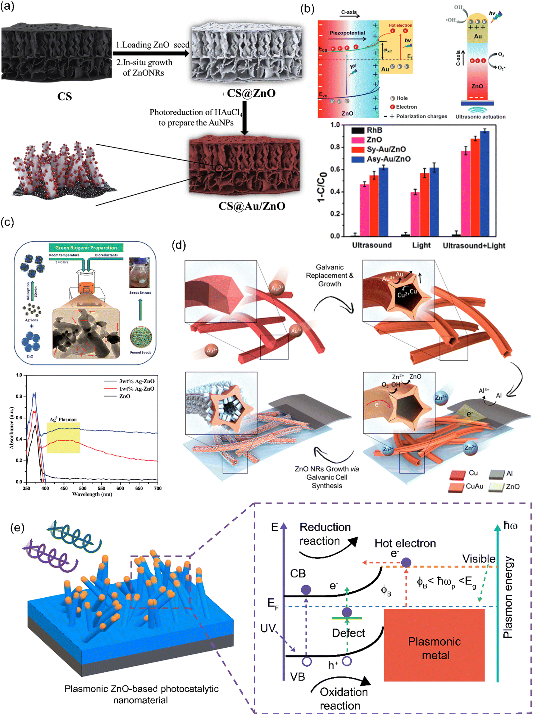 | ||
| Fig. 1 (a) Chemical growth of ZnO NRs/Au NPs on the biogenic macroporous matrix for the photocatalytic degradation of RhB and CIP. Copyrights ELSEVIER 2020.100 (b) Piezo-photocatalytic performance of asymmetrical ZnO NRs/Au NPs nanocomposites for improved exciton separation and enhanced RhB degradation. Copyrights WILEY 2020.101 (c) Plasmonic hybrid ZnO/Ag NPs for the degradation of RhB dye and CPS pesticide under natural solar irradiation. Copyrights RSC 2020.15 (d) Electrochemical synthesis of ZnO NRs over bimetallic Cu Au NSTs for plasmon-enhanced photocatalytic water splitting reaction. Copyrights ACS 2018.103 (e) A visual representation depicting how plasmonic metal–ZnO nanostructures generate visible light photocatalytic activity due to the influence of plasmon-induced electrons.104 | ||
Additionally, the piezoelectric properties of ZnO have been used synergically with the plasmonic properties of Au NPs to enhance the photocatalytic properties of ZnO-based substrates. In the work of Xiang et al.,101 the piezo-photocatalytic performance of asymmetric ZnO NRs/Au NPs nanocomposites (Asy-ZnO NRs/Au NPs) is evaluated for the degradation of RhB. The authors chemically synthesized ZnO NRs by using a conventional hydrothermal method over a conducting substrate. Then a photoreduction process was employed to deposit Au NPs only on the tip of the NRs to obtain asymmetric coverage of the semiconductor. This was achieved by the previous coverage of the 1-D nanostructures with an AZ55214E photoresist layer and a plasma etching step allowing only the tip of the rods to be exposed to the Au precursor solution. To compare the distribution of the gold in the ZnO nanostructure, ZnO NRs/Au NPs samples were prepared without the use of the AZ55214E in such a way that the deposit of the Au NPs will be carried out on the entire surface of the semiconductor material (symmetric samples; Sy-ZnO NRs/Au NPs). In addition to the improvement processes in photon absorption derived from the before mentioned SPR mechanisms, by achieving this spatially controlled Au NPs deposition, the piezoelectric potential in the c-axis of the ZnO NRs, was used to improve the charge separation process, resulting in a more efficient injection of hot electrons from the Au NPs to the ZnO NRs matrix (Fig. 1(b)). With the proposed asymmetric structure, it was observed that dye degradation reaches an efficiency of 95% in 75 minutes under a full spectrum of 100 mW cm−2 irradiation and an 80 W, 40 kHz sound actuator. Thus, the work presents a promising method for the obtention of light/sound responsive ZnO catalytic materials, where optimization in the morphological and loading parameters of the nanocomposite are still required.
Moreover, another biogenic approach for the obtention of a plasmonic ZnO photocatalyst is reported by Choudhary et al.15 They present a single-step precipitation technique using fennel seed extract as a bio-reductant for the obtention of ZnO/Ag NPs. The diffuse reflectance measurements showed the system's faculty to absorb visible light due to the SPR band of Ag (Fig. 1(c)). The hybrid nanocomposite was addressed to work at ambient conditions under the direct irradiation of natural solar light. The photocatalytic test monitored the degradation of both RhB dye and Chlorpyrifos (CPS) pesticide by using UV-Vis spectroscopic measurements, where a complete degradation in 18 min for RhB and 90% degradation of CPS in 40 min were obtained. The process is an example of alternative synthesis methods researched by various authors for the obtention of nanosized ZnO materials in a more environmentally friendly manner.27,102
Yet another example of morphological control over the growth of 1-D ZnO nanostructures in an already nanostructured substrate is presented by Tan et al.103 In this work; the authors present the electrochemical obtention of hollow bimetallic nanostructures, i.e., Copper–gold nanostartubes (Cu Au NSTs), on which ZnO NRs were galvanically synthesized using the Cu Au NSTs support as deposition cathode (Fig. 1(d)). Due to the specific morphology of the bimetallic substrate on which the ZnO nanostructures were grown, it is proposed that the stellations and cavitations of the NSTs work as regions where the electric field is strongly localized as a result of the abrupt curvature of the bimetallic structure and therefore allows a more intense SPR mechanism. As evidence, a considerable increase in the extinction coefficients of the nanocomposite in the infrared region was observed compared with the ZnO NRs system product of the SPR injection of electrons from the alloy towards the semiconductor. To evaluate the photocatalytic performance of the system, HER measurements were carried out using a 9![[thin space (1/6-em)]](https://www.rsc.org/images/entities/char_2009.gif) :1 water:methanol (as sacrificial reagent) solution under a Xe lamp (100 mW cm−2) UV-visible and visible (λ > 420 nm) irradiation, obtaining an HER of 480 μmol g−1 h−1 and 110 μmol g−1 h−1 respectively. The photocatalytic performance of the plasmonic composite is reported to be nine times larger under UV-visible irradiation than that of pristine ZnO NRs substrate.
:1 water:methanol (as sacrificial reagent) solution under a Xe lamp (100 mW cm−2) UV-visible and visible (λ > 420 nm) irradiation, obtaining an HER of 480 μmol g−1 h−1 and 110 μmol g−1 h−1 respectively. The photocatalytic performance of the plasmonic composite is reported to be nine times larger under UV-visible irradiation than that of pristine ZnO NRs substrate.
Thus, with all these aspects in mind, there are a lot of attractive advantages of these plasmon-assisted ZnO materials that have allowed the development of promising investigations in the field of photocatalysis. Fig. 1(e) presents a schematic summary of the plasmonic photocatalytic mechanism proposed by Dao et al.104 for metalized ZnO nanostructured materials. However, there is also the need to continue developing methods and techniques for precise control over plasmonic ZnO systems morphological, optoelectronic, and interfacial properties that allow the scalability and practical implementation of these materials into energy and environmental remediation applications. Table 1 summarizes various works reporting the implementation of plasmonic ZnO-based photocatalysts.
| Photocatalytic reaction | Nanomaterial employed | Synthesis technique | Morphological properties | Excitation source | Electrolyte | Evolution/degradation rate | Key features | Ref. |
|---|---|---|---|---|---|---|---|---|
| a Copper–gold nanostartubes. b Piezo-photocatalytic platform. | ||||||||
| Ciprofloxacin (CIP) degradation | ZnO/Ag/Ag3PO porous composite | Precipitation method/photoreduction | Pore size 7.5 nm Pore volume 0.023 cm3 g−1 | 300 W Xe lamp λ > 420 nm | Water | 87.1%–1 h | Enhanced photocatalytic activity under visible illumination due to synergy between SPR effect and high surface area | 14 |
| 4-Nitrophenol degradation | ZnONRs/In2S3/AgNPs composite | Sol–Gel/hydrothermal/photoreduction | ZnONRs d = 20–30 nm l = 200 nm AgNPs d = 20 nm | 300 W Xe UV-Vis/30 W UV light lamps | Water | 100%–50 min | Z-scheme heterojunction between ZnO NRs and In2S3 to promote charge carrier separation | 35 |
| Methyl orange (MO) degradation | ZnONRs/Au composite | Spray pyrolysis/hydrothermal | ZnONRs d = 50–150 nm l = 1 μm AuNPs d = 20–60 nm | 30 W Hg λmax = 550 nm/30 W Hg λmax = 365 nm | Water | UV light: 94% 3 h Visible light: 65% 3 h | Ability to generate reactive radicals due to surface hydroxylation of the composite | 90 |
| Methylene blue (MB)/methyl orange (MO) degradation | ZnONPs | Green synthesis (agro-waste extract) | d = 17 nm | 8 W Hg λ = 254 nm | Water | MB: 98.1% 60 min MO: 97.5% 100 min | Green synthesis approach for the obtention of controlled NPs with UV photocatalytic activity | 27 |
| Photocatalytic water splitting/rhodamine B (RhB)/Ciprofloxacin (CIP) degradation | ZnONRs/Au decorated CS | Hydrothermal/photoreduction | ZnONRs l = 2.1 μm w = 500 nm AuNPs d = 50 nm | 300 W Xe lamp λ = 200–1100 nm | Methanol–Water | HER: 2.384 mmol g−1 h−1 RhB: 97% 180 min CIP: 61% 180 min | ZnO catalytic performance enhanced by natural CS macroporous structure and plasmon-driven charge separation | 100 |
| Photocatalytic water splitting/rhodamine B (RhB) degradation | ZnO thin film/AgNPs composite | RF sputtering | AuNPs d = 50–100 nm | 500 W Xe lamp λ = 400–780 nm | Methanol–Water | HER; UV light: 38 μmol h−1 visible light: 24 μmol h−1 RhB; UV light: 97% visible light: 82% | High charge separation efficiency due to SPR phenomena in the ZnO interfacial region. Enhanced generation of reactive hydroxyl radicals. | 77 |
| Rhodamine B (RhB) | Asymmetric ZnONRs –AuNPs | Hydrothermal/spin coating/photoreduction | ZnONRs l = 2 μm d = 120 nm | 300 W Xe lamp; ultrasound actuation (40 kHz, 80 W)b | Water | 95% 75 min | Piezocatalytic and photocatalytic platform for improved charge carrier generation | 101 |
| Methylene blue (MB) | ZnO/AuNPs/CdS coated NRs | Hydrothermal/pulsed laser deposition | ZnONRs l = 1.3 μm d = 80 nm ZnO/Au/CdS d = 150 nm | 400 W Hg UV lamp | Aqueous solution 0.25 M Na2S and 0.35 M Na2SO3 | 82% 60 min | LSPs enhancement to the light absorption and electron transferring process resulting in higher photocatalytic and photoelectrocatalytic performance | 86 |
| Rhodamine B (RhB)/chlorpyrifos (CPS) | ZnONPs/AgNPs | Green synthesis (seed extract) | AgNPS d = 6–10 nm | Direct sunlight | Water | RhB: 98.3% 18 min CPS: 90% 40 min | Environmentally friendly nanostructured photocatalyst operating at ambient conditions | 15 |
| Hydrogen production | CuAuNSTsa/ZnNRs | Galvanic electrodeposition | CuAuNST d = 90–100 nm | 300 W Xe lamp λ > 420 nm | Methanol–Water | 480 μmol g−1 | Hollow bimetallic-semiconductor nanostructures displaying SPRs to improve HER | 103 |
3. Sensors
3.1 ZnO-based plasmonic materials for biosensing applications
The COVID-19 pandemic has shown that many of the current biotechnology techniques require continuous development to tackle this and future health emergencies, contributing to human well-being.105 One of the axes to achieve this next-generation biotechnology is the development of sensing devices for the sensitive and selective detection of multiple biological analytes (e.g., cells, nucleic acids, proteins, enzymes)106 both for prevention and early condition/disease detection.107A biosensing platform includes a layer of a transducing material that converts the chemical or physical interaction of the analyte with the sensing layer of the system. Therefore, depending on the nature of the transducer response, the sensing devices can be classified as electrochemical,108 acoustic,109,110 piezoelectric,111 optical (e.g., ellipsometric SPR, evanescent field, fluorescence sensors112–116), and photoelectrochemical.117–119 Furthermore, in some of the approaches, label-free analyte detection can be achieved.120 In many of those applications, the surface morphology of the substrate plays a crucial factor in determining the sensing performance of the platform. For this reason, much work has been reported in recent years seeking the implementation of multiple metals (e.g., Au, Ag, Cu, Al121,122), inorganic (e.g., SiO2, CdSe, CdTe, ZnO123–127), and organic (C, g-C3N4128–130) nanostructures and nanocomposites as biosensing materials.
ZnO stands out among the formerly mentioned materials due to its biocompatibility, cost-effectiveness, and biodegradability.131 In addition, its physicochemical surface properties (i.e., high isoelectric point, electric charge) and morphological tunability through various nano structuration techniques made this material an attractive option for detecting the interaction with low molecular compounds and bioanalytes for in vivo and in vitro applications.106 In addition, the obtention of a bio-selective layer on top of the semiconductor material to assure selectivity and specificity towards a particular analyte is required.109 This can be achieved by silane, thiol, and phosphoric crossing agents to functionalize the semiconductor's surface with multiple biorecognition agents (e.g., oligonucleotides, enzymes, and antibodies132–135). Recently the use of self-assembled monolayers (SAMS) as recognition elements in ZnO has been successfully accomplished.136
Consequently, multiple ZnO-based nanostructures have been developed and integrated into multiple biosensing platforms, mainly optical and electrochemical. Yet, the large bandgap of pristine ZnO makes it transparent to visible radiation. Therefore, numerous investigations have been performed to synergize the advantages that ZnO offers with the plasmonic resonance phenomena of noble metal nanostructures (Ag, Au, Pt NPs) and thin films.137–139 The optoelectronic properties of such nanostructured metallic systems allow them to display absorption bands in the visible spectrum.140 However, the lack of good adhesion to the substrate and prior biofunctionalization to work as sensing probes are among some of the limitations of these materials for bio-detection applications.
With that in mind, the integration of ZnO: Ag/Au composites into biosensing platforms as plasmonic enhanced sensing performance has been reported in multiple works; in some cases, due to the physics of the semiconductor–metal junction (Schottky barrier), electron injection to ZnO conduction band, local temperature gradients (i.e., localized adsorption and mass transport phenomena) and improved light absorption properties.141 Examples of the implementation of these metal ZnO heterostructures are the so-called SPR optical biosensors devices (Fig. 2(a)).131,142 These systems measure the change in the refractive index of interface layers with different dielectric constants. Among the reported structures, the Kretschmann configuration is recurrently used to measure the reflectance response of the plasmonic layer when irradiation is applied through a prism.132,143,144 In this configuration, the incidence angle is swiped until plasmonic resonance in the metal film is achieved. Therefore, as the resonance angle is a function of the refractive index of the sensing interface, the adsorption of biological analytes in the platform leads to a shift of the resonance angle.145,146
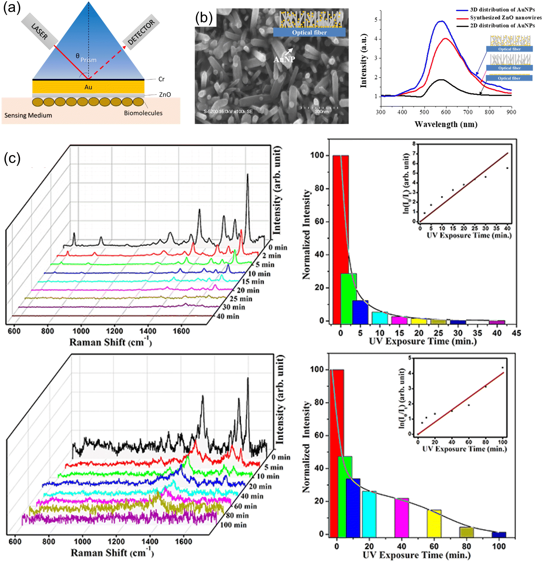 | ||
| Fig. 2 (a) Schematic of a ZnO-based SPR biosensor in Kretschmann configuration measuring the reflectance response to the adsorption of biological analytes. Copyrights IOP Publishing 2019.131 (b) Implementation of ZnONWs into fiberoptic-based SPR biosensing platform aimed at the early detection of prostate cancer. Copyrights Nature 2019.150 (c) The glucose sensing performance of nanostructured ZnO SERS substrate for glucose in multiple operation cycles using a photocatalytic cleaning approach for reusability. Copyrights AIP Publishing 2020.153 | ||
However, the use of this class of systems has proven to be limited in terms of sensitivity and selectivity. For this reason, adding biosensitive layers with better adhesion, physicochemical and morphological properties, is one of the most popular strategies for developing this type of system. In this sense, using ZnO nanostructures as immobilizing or intermediate biosensitive layers has resulted in improved detection thresholds. This has been attributed both to the increase in the surface area of the semiconductor and to the enhanced interaction with the biological analytes due to the morphological characteristic of the sensing material. ZnO-based SPR sensors are thus promising candidates for point of care (PoC) monitoring and sensitive label-free detection, and the main limitation to various practical applications is the optical response limited to the visible region. Consequently, as pointed out by some authors, effort needs to be made to achieve IR irradiated detection, which offers a more profound penetration length.147
Additionally, fiber optic-based SPR biosensing platforms have been developed where fewer bulky devices for detecting various analytes are reported.135,148 In this kind of study, the authors have focused on optimizing the sensing layers for the SPR detection mechanism of evanescent radiation propagation through the interface.114,149 On the other hand, when 0D noble metal nanostructures are used, the sensing principle is known as localized SPR (LSPR).150 For instance, in the work of Kim et al.,150 the development of a fiber-optic-based LSPR biosensor platform is presented. The sensing layer consisted of a ZnONWs: AuNPs system chemically grown on the cross-section area of an optic fiber (Fig. 2(b)). The nanocomposite aimed to detect prostate-specific antigens by an immunoassay approach, a common biomarker for the diagnosis of prostate cancer. The authors reported an improvement in the detection sensitivity of the ZnO nanowires (NWs)/Au NPS platforms in comparison with 2D multilayer systems, archiving a detection limit of 0.51 pg mL−1. Increased detection area, reduced reflectance, and enhanced light trapping properties are suspected of contributing to boosting the performance of this free-label optical sensor.
ZnO nanostructures have also been incorporated in Surface Enhanced Raman Spectroscopy (SERS) substrates to detect relevant biological elements with high specificity, where both electromagnetic and chemical enhancement factors are considered the mechanisms to achieve lower detection limits.151,152 Pal et al.153 reported the use of an Ag/ZnO NRs/Ag NPs SERS composite for the detection of hemoglobin with a LOD of 10−7.24 M (Fig. 2(c)). The growth of the ZnO 1-D nanostructures on top of an ultrathin Ag film was carried out by hydrothermal method.
Toward the characteristic LSPR behavior of a SERS platform, the NRs array was loaded with Ag NPs (d = 4–30 nm) using thermal evaporation. The proposed system exhibits high sensitivity due to the synergy between the superhydrophobicity, visible-driven LSPR, and high surface/volume ratio properties. Furthermore, the subsequent UV photocatalytic degradation of the adsorbed analytes by the SERS substrate was studied to explore the reusability and self-cleaning features of the biosensor. By performing multiple cycles of sequential detection and degradation, the reusable performance of the biosensor was demonstrated, making this a promising alternative for PoC technologies.
In addition, ZnO NRs/Ag NPs have been chemically obtained inside the glass capillary of a microfluidic system by Hao et al.154 for the SERS sensing of exosomes, single-stranded DNA (ssDNA), and E. coli bacteria. In this work, an acoustofluidic (i.e., acoustic transducer and acoustofluidic micromixer) hydrothermal synthesis approach was used to ensure precise control over the spatial distribution and morphology of the 1-D ZnO nanostructures (Fig. 3(a)). The same acoustic-assisted principle was employed for the deposition of Ag NPs on the surface of the tridimensional ZnO matrix, controlling in this way the hot-spot distribution. The resultant steric hindrance properties of the NRs network translate into an improved capability for separating the target analytes from the samples allowing superior electrostatic interaction between the analytes and the transducer. This is usually denominated in literature as biological enrichment. The nanostructured capillary coating displayed an improved label-free SERS performance due to the substrate's versatile and controllable structural design and Ag NPs distribution. The electromagnetic enhancement was also validated by computational simulations of the electric field of the ZnO NRs/Ag array.
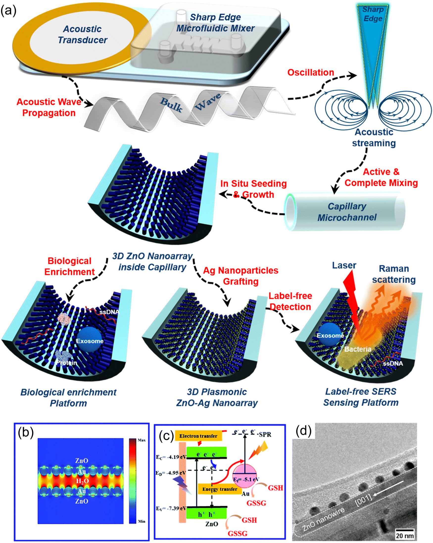 | ||
| Fig. 3 (a) Acoustofluidic driven synthesis of ZnO NRs/Ag NPs microfluidic SERS platform for detecting various biological elements. Copyrights ACS Publications 2020.154 (b and c) FDT simulation of the electromagnetic field modulation in ZnO NRs/Au NPs for photoelectrochemical detection of glutathione. Proposed electron transfer mechanism along with the obtained metal–semiconductor interface. Copyrights RCS Publishing 2019.118 (d) Pbb acetylene electric detection employing Au decorated ZnONWs. Copyrights ACS Publications 2020.160 | ||
Besides plasmonic materials contribution to optical biosensing devices, their use is also recurrent in photoelectrochemical (PEC) platforms.120 An example of this can be found in the work of Dong et al.,118 where the implementation of ZnO NRs/Au NPs photoanode is used to detect glutathione (GSH) with possible applications in early tumor detection. FDTD simulations were performed to modulate the electromagnetic field enhancement due to the LSPR mechanism when irradiated with visible light (Fig. 3(b)). The electron transfer mechanism between the composite and the analyte is represented in Fig. 3(c), where the generation of electron–hole pairs in the ZnO matrix can be observed. As the electron carriers are separated, the electrons can migrate to the FTO collector, whereas the remaining holes produce oxidized glutathione (GSSG). The incorporation of Au NPs into the ZnO array increases visible light absorption and generation of hot electrons, consequently promoting the PEC application. Table 2 presents some recent works reporting the use of ZnO plasmonic platforms for biosensing purposes. Finally, it is worth mentioning that other types of plasmonic-based sensors have been developed to detect volatile organic compounds (VOCs) and other chemical compounds.155–159 Miao et al.160 report using a ZnONWs film for the electric detection of C2H2 in the ppb concentration range (Fig. 3(d)).
| Target analyte | Nanomaterial employed | Synthesis technique | Morphological properties | Bio sensitive layer/Sensing medium | Detection platform | Performance (LOD, linear response range, sensitivity) | Key features | Ref. |
|---|---|---|---|---|---|---|---|---|
| a PTCA: perylene-3,4,9,10-tetracarboxylicacid; BSA: Bovine serum albumin; BP: Black phosphorus; ssDNA: single-stranded DNA; PBS: Phosphate-buffered saline; AOx: Ascorbate oxidase; GOx: Glucose oxidase. | ||||||||
| Thrombin | ZnONRs/PTCA/AuNPs | Hydrothermal | d = 69 nm | Thrombin aptamers | Photoelectrochemical | 33 fM/0.0001–5 nM | SPR-enhanced electron injection to the photoactive PTCA layer | 117 |
| Nanosized exosomes | ZnONRs/AgNPs covered glass capillary | Hydrothermal | d = 200 nm l = 3 μm | Direct contact with the analyte solution | Acustofluidic SERS microchannel | 20 exosomes μL−1/102–108 exosomes μL−1 | SERS enhancement due to acoustofluidic driven analyte agglomeration | 110 |
| BSAa | Prism-ZnO/Au/WSe2/BPa multilayer film | Sputtering/thermal vapor deposition | ZnO = 40 nm Au = 42 nm WSe2 = 0.7 nm BP = 0.53 nm | Water | Kretschmann SPR sensor | 101.5°/RIU | Multilayer structures increase electric field intensity improving conventional SPR sensitivity | 146 |
| ssDNAa | Prism-Au/ZnO/Graphene multilayer film | Not specified | Au = 44 nm ZnO = 6 nm | Single-stranded DNA hybridization probe/PBSa | Kretschmann SPR sensor | 141.9°/RIU | Synergic performance of ZnO-graphene adhesion layer | 132 |
| Ascorbic acid | ZnONPs/AuNPs | Commercially available ZnONPs (Sigma-Aldrich) | AuNPS d = 11 nm ZnONPs d < 50 nm | AOxa enzyme | LSPR optical fiber biosensor | 25.78 μM/10–200 μM | Micromaquinated optical fiber with immobilized NPs to increase biocompatibility and plasmon behavior | 149 |
| Glucose | ZnO/Ag films | Magnetron Sputtering | Ag = 45 nm ZnO = 5 nm | GOxa enzyme/PDMS | SPR optical fiber biosensor | 16.24 μM | Dual channel sensor for the detection of glucose taking temperature compensation into account for accurate analyte measurements | 135 |
| Hemoglobin | Ag film/ZnONRs/AgNPs | Hydrothermal (ZnONRs); Thermal evaporation (AgNPs) | ZnONRs: d = 54 nm l = 991 nm AgNPs: d = 4–30 nm | Direct contact with the analyte solution | SERS substrate | 10−7.24 M | UV photocatalytic degradation of the analyte by the nanocomposite allows the biosensor reusability | 153 |
| Exosomes, ssDNA and E. coli | ZnONRs/AgNPs-coated glass capillary | Hydrothermal (ZnONRs); Nitrate reduction (AgNPs) | ZnONRs: d = 163–508 nm l = 1–10 μm | Direct contact with the analyte solution | SERS substrate | Exosome: 104–108; ssDNA: 0.1 nM–1 μM; E. coli: 50–105 bacteria | SERS enhancement due to acoustofluidic driven analyte enrichment and homogeneous AgNPs deposition on ZnO 3D matrix | 154 |
| Glutathione | ZnONRs/AuNPs | Hydrothermal (ZnONRs); Sputtering (AuNPs) | ZnONRs: d = 150 nm l = 1.2 μm AuNPs: d = 5 nm | PBS | Photoelectrochemical | 2.7 μM/10–800 μM | SPR boosted electron transfer leading to photocurrent enhancement: potential application in early tumor detection | 118 |
| Dopamine | Matchstick-shaped ZnONRs/AuNPs | High-temperature solution method | ZnONRs: d = 9 nm l = 46 nm AuNPs: d = 8 nm | Direct contact with the analyte solution | SERS substrate | 1 × 10⁻⁵ M | Harnessing of the hot electron transfer process to obtain SERS response in biocompatible and reusable semiconducting platform | 141 |
As seen from all the mentioned works, developing promising biosensing technologies integrating plasmonic ZnO nanostructures is a current effort where high sensitivity, selectivity, reusability, and mass scalability are among the main goals to achieve in order to have commercially available devices. Hence, the implementation of these plasmonic systems is not limited to biosensing applications but can also be extrapolated to chemosensing, energy production, and photonic devices.
3.2 ZnO as chemiresistive ozone (O3) gas sensors
ZnO is the second most studied metal oxide semiconductor aiming for application as a resistive gas sensor.4,161,162 In 1962, a ZnO thin film was the first material reported to change its conductivity due to the interaction with a gaseous phase.163 As with other wide bandgap materials, the high electron mobility makes it a promising material for the development of transparent electronics and gas sensing applications.164,165 The easy and/or low-cost synthesis methodologies to prepare ZnO, and the high sensitivity of the undoped material, comparable with the performance of materials commercially available, make the ZnO a potential material for applications as a gas-sensing layer.Nowadays, implementing gas sensor technology becomes essential to achieve a truly sustainable society with environmental safety and quality of living conditions. Numerous studies highlight the influence on human health and the environment of certain air pollutants such as H2S, NOx, O3, CO, and some Volatile Organic Compounds (VOCs).166,167 Among the noxious species, O3 is one of the most significant concerns because it influences human health as well as damages ecosystems when above a certain concentration level.168,169
According to the World Health Organization (WHO), even in low concentrations (from 50 ppb), ground-level ozone might negatively impact human health. Despite its usefulness as a disinfectant agent and to oxidize organic pollutants in water treatment processes, the ozone can damage the tissues of the respiratory tract, causing inflammation and irritation, leading to respiratory diseases.170,171
In a recent study, Zoran and co-workers172 reported the relationship between ground levels of O3 and NO2 for COVID-19. It was observed that the increasing O3 ground level is directly associated with a subsequent negative impact on human respiratory health, and also, the increase in COVID-19 cases was confirmed.
ZnO-based compounds have been extensively studied for the detection of various analytes.173,174 However, few of these studies have been devoted to the detection of sub-ppm O3 gas levels. Another aspect that has been little addressed in studies dealing with the application of ZnO as an O3 gas sensor is the synthesis method which would allow obtaining a gas sensor device presenting the best sensing performance in terms of sensitivity, working temperature, and selectivity. The development of novel synthesis methodologies, which allowed to obtain thin films and nanostructured ZnO exhibiting distinct morphologies and particle sizes, has demonstrated the potential of ZnO in detecting sub-ppm levels of O3 gas. Table 3 displays the O3 sensing performance of ZnO obtained by different chemical/physical techniques.
| Processing method | Operating temperature (°C) | Minimum of O3 level detected (ppb) | Ref. |
|---|---|---|---|
| CVD | 200 | 280 | 35 |
| Hydrothermal | 250 | 60 | 90 |
| RF-magnetronsputtering | 300 | 60 | 27 |
| Microwave-assisted hydrothermal | 200 | 100 | 101 |
| Polymeric precursor method | 250 | 33 | 86 |
| Hydrothermal | RT/UV | 30 | 86 |
| CVD | RT | 1000 | 86 |
| Hydrothermal | RT/UV | 60 | 15 |
| RF-magnetron sputtering | 300 | 30 | 15 |
| RF-magnetron sputtering | 300 | 60 | 15 |
Chien and co-workers175 grew 1-D ZnO NRs via the chemical vapor deposition (CVD) method aiming at the application as a gas-sensing layer to O3. Their results indicated that the NRs exhibited a high sensing activity with a fast response and recovery times at room temperature under UV illumination. The superior sensor performance to O3 detection was linked to the low defect density and high electron mobility of the single-crystal NRs. In another study, Acuautla and co-workers176 reported the O3 sensing properties of commercial ZnO NPs deposited onto a flexible substrate via the drop coating method. They demonstrated that ZnO NPs exhibited an excellent sensing performance to different O3 levels (5 to 300 ppb) at an operating temperature of 200 °C.
Over the last decades, Katsarakis and co-workers employed different methods to obtain ZnO nanostructures applied as photoreduction O3 sensors.177–181 For instance, in 2007, Katsarakis et al.180 studied the effect of deposition time on the morphological and sensing properties of ZnO nanostructures obtained via aqueous chemical growth. The authors reported that the O3 sensing performance of these nanostructures depends on surface morphology, substrate coverage, and average thickness, which were influenced by the deposition time. They conclude that the flowerlike nanostructured deposited for 5 h exhibited significantly enhanced gas-sensing performance towards O3, which was attributed to their higher surface-to-volume ratio. The ZnO-based nanostructured gas sensor has been prepared to employ various methods that yield unique morphologies, providing different sensing performances. Among the techniques that can be used to obtain ZnO sensing material directly on the flat substrate, such as the conventional hydrothermal route, the polymeric precursor method, and RF magnetron sputtering technique.
The hydrothermal method has been employed in processing inorganic/ceramic powders at relatively low temperatures (<200 °C). Some researchers have also used such a method for growing a variety of highly c-axis-oriented materials directly onto a substrate surface.182–184 There are several studies on applying the hydrothermal method to obtain textured films with perpendicular orientation concerning the substrate surface.185,186 Recently, we devoted efforts to understanding the short-range order structure and surface properties in ZnO and CoxZn1−xO thin films deposited on the substrate via the chemical deposition method. In another work,187 Co0.05Zn0.95O thin film was deposited via spray-pyrolysis technique for application as an O3 gas sensor. The sensing layer was observed to be sensitive to ozone with a detection limit of around 20 pbb of O3 gas, demonstrating its potential as an O3 gas sensor.
Although the deposition of thin films by chemical methods offers advantages over physical processing techniques, including low cost, simplicity, and a high degree of control stoichiometry.188,189 It is well established that films deposited by physical methods such as molecular beam epitaxy, pulsed laser deposition, direct current (DC) magnetron sputtering, and RF magnetron sputtering exhibit excellent micro- and nanostructural properties. On the other hand, physical methods are usually performed under vacuum conditions in a well-controlled atmosphere, which implies high energy consumption and more expensive equipment.190 Substantial research has been conducted on the fabrication of various nanostructured materials using RF magnetron sputtering for application in monitoring H2, NOx, and O3 gases. However, this technique has not been well explored in the development of O3 gas sensors based on ZnO thin films.
In 2020, it was reported the effect of morphology on the O3 gas sensing properties of porous zinc oxide sputtered films.191 These results show that both the porosity and the feature size have an essential relation to the sensing performance. For instance, the optimum sensing performance was found to be at the apparent maximized surface area, indicating that the sensitivity improvement can be controlled utilizing several deposition parameters previously determined.
Although several researchers have investigated the ZnO as a gas-sensing layer for harmful gases, a comparative study of the latest developments in ZnO-based chemiresistive gas sensors prepared via different methodologies for O3 detection is still lacking. Motivated by these considerations, here is a background review of chemiresistive ozone gas sensors based on ZnO nanostructured obtained via different physical and chemical methods to investigate which synthesis method allowed a better sensing performance in terms of operating temperature and gas selectivity.
The growth of 1-D ZnO nanorods directly into interdigitated electrodes via the hydrothermal method promoted an easy integration of sensing components into the O3 gas sensor device for practical applications.192Fig. 4(a) shows the schematics of the glass bottle used as an autoclave for a hydrothermal chemical reaction to obtain the ZnO nanorods onto a gas sensor device. A detailed description of the synthesis procedure can be found in ref. 192. The SEM micrograph and gas sensing properties of ZnO nanorods grown by following this methodology are shown in Fig. 4(b–e). As can be seen in Fig. 4(c), the 1-D ZnO NR-like structures exhibited a good sensor response (S = RO3/Rair) towards 0.1 ppm of O3 gas at an operating temperature of 250 °C. Additionally, it was found that the ZnO NRs had good sensitivity to O3 at room temperature under UV illumination. This study aimed to provide a simple, low-cost, and efficient processing method for obtaining O3 gas sensors based on hierarchical 1-D ZnO NR-like structures.
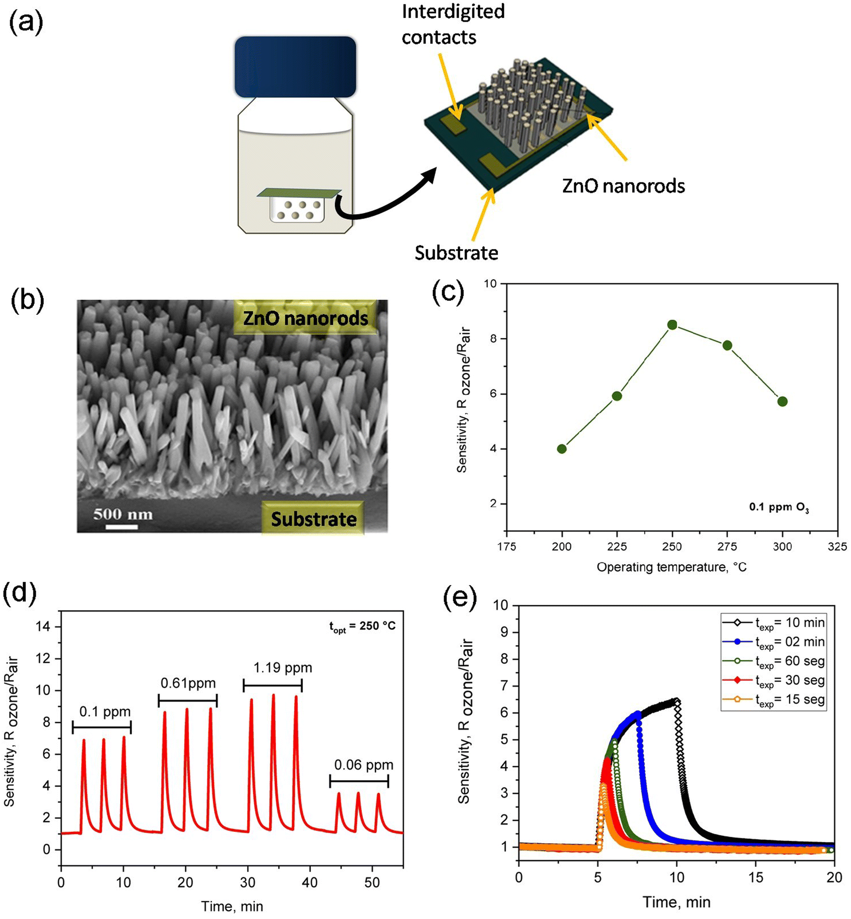 | ||
| Fig. 4 ZnO NRs film prepared via hydrothermal method. (a) Schematics illustrations of glass bottle used as an autoclave for hydrothermal chemical reaction and the gas sensor device structure, (b) FESEM images of the sample cross-section, (c) sensing response at different operating temperatures, (d) dynamic response-recovery curves as a function of the O3 gas level, and (e) Electrical resistance of the sample exposed to ozone gas during different time intervals. Reproduced from ref. 192 with permission from the Royal Society of Chemistry. | ||
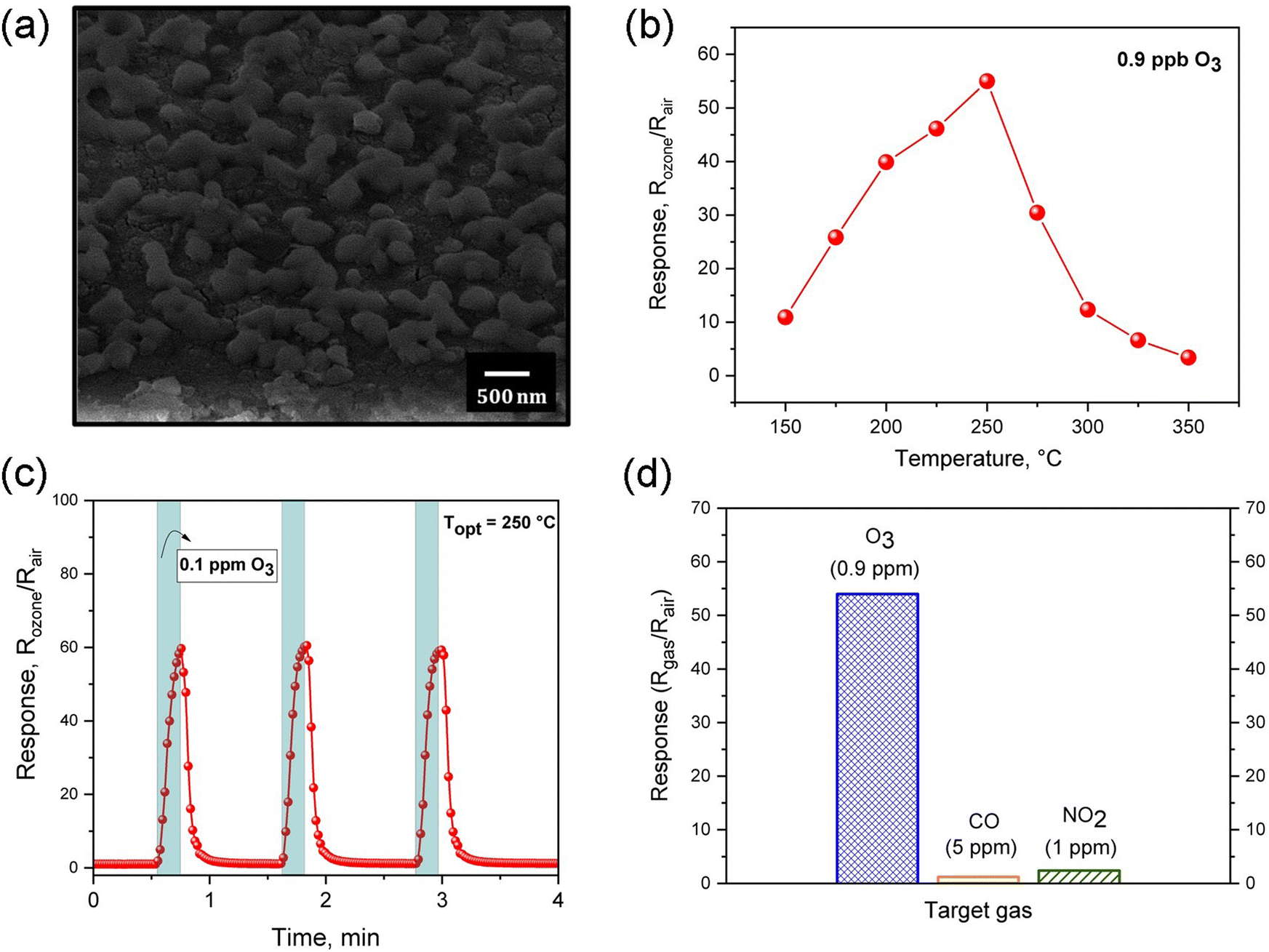
The polymeric precursor method also represents a relatively low-cost alternative to achieve good-quality samples with remarkable sensing properties by using a simple deposition method such as spin-coating, dip-coating, and spray-coating. In a previous report,193 we described the synthesis of the pristine ZnO and Co-doped ZnO nanostructured using the polymeric precursor method. In this case, the obtained polymeric resin was deposited on the SiO2/Si substrate via spin-coating. The FESEM micrograph and gas sensing properties of pristine ZnO thin film are shown in Fig. 5. These nanostructured thin films exhibited an operating temperature of 250 °C, high sensitivity, and excellent selectivity to O3. Also, the long-term stability was evaluated for 9 months. Its good O3 sensing performance was attributed to the effect of Co ions on the ZnO electronic surface properties and the increased oxygen vacancies concentration.
 | ||
| Fig. 5 Nanostructured ZnO thin film prepared via polymeric precursor method. (a) FESEM images (b) sensing response at different operating temperatures, (c) material selectivity towards different gas analytes, and (d) dynamic response-recovery curves as a function of the O3 gas level. | ||
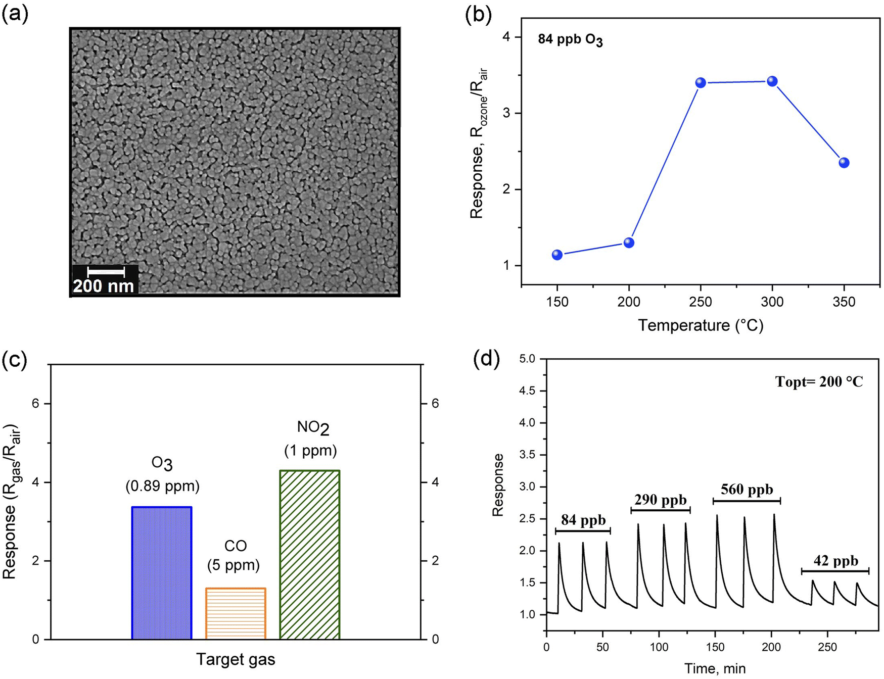
More recently, it was demonstrated that ZnO nanostructured thin film deposited by a sputtering technique using a metallic Zn target could also be considered an excellent candidate for O3 sensing layers. The gas-sensing performance of ZnO film towards O3 gas and its microstructural properties are shown in Fig. 6. As can be seen in Fig. 6(a), the nanostructured film is formed by grains of a mean size of approximately 124 nm grown over a continuous thin and densely packed layer. Regarding the sensing performance, ZnO sputtered samples were exposed to 0.9 ppm of O3 for 15 s at different operating temperatures, achieving the highest sensor response (S = 55) at 250 °C, as shown in Fig. 6(b). Fig. 6(c) presents the reversible cycles of the response curve, indicating good stability and reproducibility at 250 °C. The selectivity was also evaluated by exposing the sensor to oxidizing (O3 and NO2) and reducing (CO) gases at 250 °C, as can be seen in Fig. 6(c). The values found were around S = 55 for O3, S = 2.4 for NO2, and S = 1.2 for CO, demonstrating a good degree of ZnO-sputtered thin film's selectivity. Fig. 7 shows a schematic illustration of the ozone-sensing mechanism of the ZnO rod-like crystals. The sensing mechanism illustrated in Fig. 7 of the ZnO nanorods upon exposure to O3 gas can be explained by the following reactions.193 First, when the ZnO nanorods were exposed to air, the oxygen molecules adsorbed on the semiconductor surface.
| O2(g) → O2(ads) | (2) |
| O2(ads) + 2e− → 2O−(ads) | (3) |
| O3(g) + e− → − O3−(ads) | (4) |
| O3−(ads) + O−(ads) + 2e− → O2(g) + 2O2−(ads) | (5) |
 | ||
| Fig. 6 ZnO thin film prepared via an RF-magnetron sputtering. (a) FESEM micrograph (b) sensing response at different operating temperatures, (c) dynamic response-recovery curves to 0.1 ppm of ozone, and (d) material selectivity towards different gas analytes. | ||
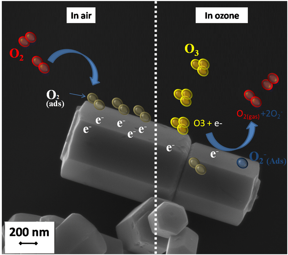 | ||
| Fig. 7 FESEM image of ZnO nanorods synthesized via a hydrothermal method and the schematic ozone sensing mechanism. | ||
Table 4 compares the sensing performance of gas sensors based on ZnO nanostructures synthesized by different synthesis methods when exposed to 15 s to 0.9 ppm of ozone at a working temperature of 250 °C. The gas-sensing experiments revealed that the RF-sputtered ZnO sample exhibited a superior gas-sensing response compared to the ZnO prepared by the other two methods. The response and recovery time were also compared, and the three samples presented a fast response time and total reversibility; however, the thin film sample prepared via the polymeric precursor method showed the highest recovery time. Indeed, the morphology, thickness, and microstructure of the ZnO sensing layer play a key role in obtaining superior gas-sensing properties. In overview, the preparation method can influence the gas sensing performance, since the sensor response depends on sensitive films' physical and chemical properties. Therefore, a good knowledge of the details of the preparation method will undoubtedly allow for obtaining more efficient gas sensor devices with specific sensing properties.
| Preparation method | O3 sensor response (Rgas/Rair) | Response time (s) | Recovery time (s) |
|---|---|---|---|
| Hydrothermal | 2 | 3 | 5 |
| Polymeric precursor method | 9 | 10 | 60 |
| RF-magnetron sputtering | 50 | 8 | 4 |
Conclusions and perspectives
As has been discussed in the present work, the use of ZnO-based nanomaterials in various fields of applications provides promising results due to the versatile properties of the material. Still, challenges and goals are yet to be addressed for the practical implementation of these systems, implying future research and development.Compared to other materials, ZnO photocatalytic applications thrive in their cost effectiveness, band structure, and tunable morphology. Even so, its band gap and carrier recombination rate are among the main limitations of its performance in solar-driven photocatalysis. Thus, doping, metallization, and nanostructure formation strategies are widely reported in the literature to improve catalytic activity. For instance, substitutional doping in ZnO with Ce2+, Cu2+, or Ag2+ (with or without the participation of co-dopants) ions improves the photocatalytic rate for hydrogen production. Nevertheless, it is vital to have precise control over doping processes since it can be responsible for counterproductive effects on performance, such as the generation of recombination centers or states with low reductive potential. Doping has also proved to be an efficient way to reduce particle size and then increase the surface area available for photocatalytic reactions.
Furthermore, recent trends in this field include the development of hybrid ZnO-based nanostructures, which can be achieved using organic/inorganic porous or texturized matrixes as substrates in low-temperature solutions and electrochemical growth techniques. Biogenic approaches for the environmental synthesis of nanostructured ZnO platforms have also been explored. These works report a significant increase in surface area available for photocatalytic reactions. Additionally, many authors have leveraged the precise morphology of ZnO nanoscaffolds to control the spatial distribution of novel metal NPs in plasmonic-enhanced photocatalytic substrates. Efficient charge separation, Schottky union formation, hot electron generation, and improved mass transfer from the media to the catalyst are among the main mechanisms responsible for extended photocatalysis in ZnO: metal composites over a wide range of visible spectrum illumination.
On the other hand, the transducer behavior of nanostructured ZnO has been exploited for the development of biosensing systems. This is because the material contributes in terms of surface area increment and tunable biofunctionalization with a wide variety of biorecognition layers. In this way, integrating hybrid systems composed of plasmonic metals and ZnO nanostructures has stood out in the field of optical and electrochemical biosensing. Thus, contributing to common limitations of noble metals, such as lack of adhesion. Implementing ZnO nanostructured morphologies into surface plasmon resonance (kresshman and fiber optic configurations), SERS, and microfluidic biosensors have been demonstrated to improve sensing performance both in terms of selectivity, sensitivity, and reusability. All of the formerly mentioned achievements could be targeted toward high-impact diseases and the development of point-of-care technologies.
Finally, undoped ZnO layers are also suitable gas sensing materials required for environmental safety and assuring live wellness. On this matter, O3 has significant relevance due to its environmental and health impact, and its detection in sub-ppm concentrations remains challenging. Therefore, studies on the sensing performance of ZnO materials towards O3 are not near to being exhausted but are yet to be explored in detail. Currently, low-defect density, high-electron mobility, high surface-to-volume ratio, porosity, and crystallinity are among the relevant factors affecting the chemoresistance of ZnO-based sensors. Both physical and chemical synthesis techniques have been proven to obtain ZnO micro and nanostructures with controlled and suitable properties for O3 sensing applications. This sometimes allows the platforms to accomplish good selectivity and total reversibility. Nevertheless, low-temperature solution-based techniques that allow the growth of ZnO nanomaterials on electrodes promise to be a simple and low-cost approach to integrate these materials into practical gas sensors.
Conflicts of interest
There are no conflicts to declare.Acknowledgements
The authors are grateful to the second research collaboration fund 2019 of the Unión Iberoamericana de Universidades. F. G. acknowledges support from the AGAUR grant no. 2021SGR00147. A. G. M. thankfully acknowledges CONACyT Grant CVU 860916. G. S. acknowledges Conacyt PN 4797 and DGAPA IG100320 projects. A. D., thanks for the DGAPA IA 100123 funding. V. R. M., A. C. C. and L. F. S. acknowledge the financial support of the Brazilian research funding institutions: FAPESP (grants No 2013/07296-2, 2018/18208-0, No2022/02927-3) and CNPq (grants No. 405140/2018-5 and 426511/2018-2).References
- F. Güell, A. Cabot, S. Claramunt, A. O. Moghaddam and P. R. Martínez-alanis, Nanomaterials, 2021, 11, 1–17 CrossRef PubMed.
- A. Galdámez-Martinez, G. Santana, F. Güell, P. R. Martínez-Alanis and A. Dutt, Nanomaterials, 2020, 10, 857 CrossRef PubMed.
- G. Murillo, E. Leon-Salguero, P. R. Martínez-Alanis, J. Esteve, J. Alvarado-Rivera and F. Güell, Nano Energy, 2019, 60, 817–826 CrossRef CAS.
- E. Navarrete, F. Güell, P. R. Martínez-Alanis and E. Llobet, J. Alloys Compd., 2022, 890, 161923 CrossRef CAS.
- D. Zhang, L. Yu, D. Wang, Y. Yang, Q. Mi and J. Zhang, ACS Nano, 2021, 15, 2911–2919 CrossRef PubMed.
- D. Wang, D. Zhang, J. Guo, Y. Hu, Y. Yang, T. Sun, H. Zhang and X. Liu, Nano Energy, 2021, 89, 106410 CrossRef CAS.
- D. Zhang, J. Wu, P. Li, Y. Cao and Z. Yang, ACS Appl. Mater. Interfaces, 2019, 11, 31245–31256 CrossRef CAS PubMed.
- D. Wang, D. Zhang, Q. Pan, T. Wang and F. Chen, Sens. Actuators, B, 2022, 371, 132481 CrossRef CAS.
- D. Wang, D. Zhang, M. Tang, H. Zhang, T. Sun, C. Yang, R. Mao, K. Li and J. Wang, Nano Energy, 2022, 100, 107509 CrossRef CAS.
- V. Gerbreders, M. Krasovska, E. Sledevskis, A. Gerbreders, I. Mihailova, E. Tamanis and A. Ogurcovs, CrystEngComm, 2020, 22, 1346–1358 RSC.
- W. Chatchawal, S. Kittitat, M. Andreas, B. Iris Amarilio, T. Shoshana, L. Yeshayahu, Z. Margit, C. Wongchoosuk, K. Subannajui, A. Menzel, I. A. Burshtein, S. Tamir, Y. Lifshitz and M. Zacharias, J. Phys. Chem. C, 2011, 115, 757–761 CrossRef.
- N. Babayevska, Ł. Przysiecka, I. Iatsunskyi, G. Nowaczyk, M. Jarek, E. Janiszewska and S. Jurga, Sci. Rep., 2022, 12, 1–13 CrossRef PubMed.
- S. Raha and M. Ahmaruzzaman, Nanoscale Adv., 2022, 4, 1868–1925 RSC.
- C. Y. Du, J. H. Song, S. Y. Tan, L. Yang, G. L. Yu, H. Chen, L. Zhou, Z. Zhang, Y. Zhang, Y. H. Su, X. F. Wen and S. T. Wang, Mater. Chem. Phys., 2021, 260, 124136 CrossRef CAS.
- M. K. Choudhary, J. Kataria, V. K. Bhardwaj and S. Sharma, Nanoscale Adv., 2019, 1, 1035–1044 RSC.
- G. El Fidha, N. Bitri, F. Chaabouni, S. Acosta, F. Güell, C. Bittencourt, J. Casanova-Chafer and E. Llobet, RSC Adv., 2021, 11, 24917–24925 RSC.
- K. Kacem, J. Casanova-Chafer, A. Hamrouni, S. Ameur, F. Güell, M. F. Nsib and E. Llobet, Bull. Mater. Sci., 2023, 46, DOI:10.1007/s12034-023-02913-7.
- P. Gaffuri, T. Dedova, E. Appert, M. Danilson, A. Baillard, O. Chaix-Pluchery, F. Güell, I. Oja-Acik and V. Consonni, Appl. Surf. Sci., 2022, 582, 152323 CrossRef CAS.
- W. K. Tan, H. Muto, T. Ito, G. Kawamura, Z. Lockman and A. Matsuda, J. Nanosci. Nanotechnol., 2019, 20, 359–366 CrossRef PubMed.
- Y. H. Chiu, K. D. Chang and Y. J. Hsu, J. Mater. Chem. A, 2018, 6, 4286–4296 RSC.
- Y. Q. Sun, B. Xu, Q. Shen, L. F. Hang, D. D. Men, T. Zhang, H. L. Li, C. C. Li and Y. Li, ACS Appl. Mater. Interfaces, 2017, 9, 31897–31906 CrossRef CAS PubMed.
- K. Portillo-Cortez, A. Martínez, M. Bizarro, M. F. García-Sánchez, F. Güell, A. Dutt and G. Santana, Front. Chem., 2021, 8, 1–11 RSC.
- W. W. Zhang, W. Z. Wang, H. L. Shi, Y. J. Liang, J. L. Fu and M. Zhu, Sol. Energy Mater. Sol. Cells, 2018, 180, 25–33 CrossRef CAS.
- K. Munawar, M. A. Mansoor, M. M. Olmstead, T. Zaharinie, M. N. M. Zubir, M. Haniffa, W. J. Basirun and M. Mazhar, Mater. Chem. Phys., 2020, 255, 123220 CrossRef CAS.
- J. B. Lee, S. Choi, J. Kim and Y. S. Nam, Nano Today, 2017, 16, 61–81 CrossRef CAS.
- Q. Guo, L. Fu, T. Yan, W. Tian, D. Ma, J. Li, Y. Jiang and X. Wang, Appl. Surf. Sci., 2020, 509, 144773 CrossRef CAS.
- B. P. Narasaiah and B. K. Mandal, Mater. Res. Express, 2020, 7, 024001 CrossRef CAS.
- A. Fujishima and K. Honda, Nature, 1972, 240, 226–229 Search PubMed.
- Y. J. Liu, C. X. Xu, Z. Zhu, J. F. Lu, A. G. Manohari and Z. L. Shi, Mater. Res. Bull., 2018, 98, 64–69 CrossRef CAS.
- L. Ma and S. J. Ding, Mater. Lett., 2018, 217, 255–258 CrossRef CAS.
- S. Sohrabnezhad and S. Taghaddosnezhad, Appl. Clay Sci., 2018, 157, 130–138 CrossRef CAS.
- C. Yao, J. Lin, L. Li, K. Jiang, Z. Hu, N. Xu, J. Sun and J. Wu, Phys. Status Solidi, 2021, 218, 2000737 CrossRef CAS.
- Y. Zhang, J. B. Zhou, Z. Li and Q. Q. Feng, J. Mater. Sci., 2018, 53, 3149–3162 CrossRef CAS.
- Y. Han, C. B. Yao, Y. Cai, S. B. Bao and G. Q. Jiang, J. Alloys Compd., 2020, 835, 155339 CrossRef CAS.
- J. W. Wei, S. M. Wei, N. Chang, H. T. Wang and J. M. Zhang, Nanotechnology, 2021, 32, 105706 CrossRef CAS PubMed.
- R. Kant, S. Pathak and V. Dutta, Sol. Energy Mater. Sol. Cells, 2018, 178, 38–45 CrossRef CAS.
- S. S. Wu, R. Wang, N. Y. Tan, D. H. Lan, C. T. Au and B. Yi, Mater. Res. Express, 2018, 5, 125009 CrossRef.
- M. B. Tahir, G. Nabi, M. Rafique and N. R. Khalid, Int. J. Environ. Sci. Technol., 2017, 14, 2519–2542 CrossRef CAS.
- Y. Li, Q. Yang, Z. Wang, G. Wang, B. Zhang, Q. Zhang and D. Yang, Inorg. Chem. Front., 2018, 5, 3005–3014 RSC.
- P. Raizada, A. Sudhaik, S. Patial, V. Hasija, A. A. Parwaz Khan, P. Singh, S. Gautam, M. Kaur and V. H. Nguyen, Arabian J. Chem., 2020, 13, 8424–8457 CrossRef CAS.
- C. Karunakaran, I. JebaSing and P. Vinayagamoorthy, J. Nanosci. Nanotechnol., 2019, 19, 4064–4071 CrossRef CAS PubMed.
- S. Y. Fu, J. R. Chen, H. S. Han, W. Z. Wang, H. L. Shi, J. L. Fu and Y. Jia, J. Alloys Compd., 2019, 799, 183–192 CrossRef CAS.
- G. H. Qin, X. X. Sun, Y. Y. Xiao and F. S. Liu, J. Alloys Compd., 2019, 772, 885–899 CrossRef CAS.
- N. A. Alomair and H. H. Mohamed, Mater. Res. Express, 2019, 6, 115061 CrossRef CAS.
- K. S. Seelan, K. Ravichandran, P. Kavitha and P. K. Praseetha, Appl. Phys. A: Mater. Sci. Process., 2020, 126, 750 CrossRef.
- E. Abbasi, M. Haghighi, R. Shokrani and M. Shabani, Mater. Res. Bull., 2020, 129, 110880 CrossRef CAS.
- C. H. Ma, Z. F. Liu, Z. F. Tong, C. C. Han and Q. J. Cai, Appl. Phys. A: Mater. Sci. Process., 2019, 125(7) DOI:10.1007/s00339-019-2742-2.
- L. Yin, C. Liu, J. Wang, F. Wang, S. Chai, D. Zhang, X. Kong, H. Li and J. Huang, Mater. Sci. Eng., B, 2019, 251, 114449 CrossRef CAS.
- H. J. Jung, R. Koutavarapu, S. Lee, J. H. Kim, H. C. Choi and M. Y. Choi, J. Alloys Compd., 2018, 735, 2058–2066 CrossRef CAS.
- Y. C. Chang, J. Y. Guo and C. M. Chen, Mater. Lett., 2017, 209, 60–63 CrossRef CAS.
- IEA, The Future of Hydrogen, https://www.iea.org/reports/the-future-of-hydrogen, (accessed 17 June 2022).
- NIST, NIST Chemistry Webbook, https://webbook.nist.gov/chemistry/, (accessed 17 June 2022).
- C.-H. Liao, C.-W. Huang and J. C. S. Wu, Catalysts, 2012, 2, 490–516 CrossRef CAS.
- C. Ding, K. L. Yang and J. He, Biological and fermentative production of hydrogen, 2016 Search PubMed.
- I. Dincer and C. Acar, Int. J. Hydrogen Energy, 2014, 40, 11094–11111 CrossRef.
- A. Galdámez-Martínez, Y. Bai, G. Santana, R. S. Sprick and A. Dutt, Int. J. Hydrogen Energy, 2020, 45, 1–10 CrossRef.
- Z. I. Önsan, Turk. J. Chem., 2007, 31, 531–550 Search PubMed.
- Y. Yu, G. Chen, Y. Zhou and Z. Han, J. Rare Earths, 2015, 33, 453–462 CrossRef CAS.
- B. Ma, H. Xu, K. Lin, J. Li, H. Zhan, W. Liu and C. Li, ChemSusChem, 2016, 9, 820–824 CrossRef CAS PubMed.
- G. Cernuto, N. Masciocchi, A. Cervellino, G. M. Colonna and A. Guagliardi, J. Am. Chem. Soc., 2011, 133, 3114–3119 CrossRef CAS PubMed.
- Y. C. Sharma, A. Kumar, R. Prasad and S. N. Upadhyay, Renewable Sustainable Energy Rev., 2017, 74, 89–103 CrossRef CAS.
- T. Hou, S. Zhang, Y. Chen, D. Wang and W. Cai, Renewable Sustainable Energy Rev., 2015, 44, 132–148 CrossRef CAS.
- S. Bhatia and N. Verma, Mater. Res. Bull., 2017, 95, 468–476 CrossRef CAS.
- N. Kannadasan, N. Shanmugam, S. Cholan, K. Sathishkumar, G. Viruthagiri and R. Poonguzhali, Mater. Charact., 2014, 97, 37–46 CrossRef CAS.
- S. Anandan and M. Miyauchi, Phys. Chem. Chem. Phys., 2011, 13, 14937–14945 RSC.
- M. Samadi, M. Zirak, A. Naseri, E. Khorashadizade and A. Z. Moshfegh, Thin Solid Films, 2016, 605, 2–19 CrossRef CAS.
- I. Ahmad, M. S. Akhtar, M. F. Manzoor, M. Wajid, M. Noman, E. Ahmed, M. Ahmad, W. Q. Khan and A. M. Rana, J. Rare Earths, 2021, 39, 440–445 CrossRef CAS.
- G. Kale, S. Arbuj, U. Kawade, S. Kadam, L. Nikam and B. Kale, J. Mater. Sci.: Mater. Electron., 2019, 30, 7031–7042 CrossRef CAS.
- P. Jongnavakit, P. Amornpitoksuk, S. Suwanboon and N. Ndiege, Appl. Surf. Sci., 2012, 258, 8192–8198 CrossRef CAS.
- M. N. Huda Liton, A. K. Mohammad Farid Ul Islam, M. Kamruzzaman, M. K. Rahman Khan, M. Al Helal and M. M. Rahman, Mater. Chem. Phys., 2020, 242, 122463 CrossRef CAS.
- V. Vaiano and G. Iervolino, Appl. Sci., 2019, 9(13), 2741 CrossRef CAS.
- K. G. Kanade, B. B. Kale, J. O. Baeg, S. M. Lee, C. W. Lee, S. J. Moon and H. Chang, Mater. Chem. Phys., 2007, 102, 98–104 CrossRef CAS.
- I. Ahmad, E. Ahmed, M. Ullah, A. M. Rana, M. F. Manzoor, M. A. Rasheed, A. S. Malik, N. R. Khalid, M. Ahmad and U. Mehtab, J. Ovonic Res., 2018, 14, 415–427 CAS.
- Ö. A. Yildirim, H. E. Unalan and C. Durucan, J. Am. Ceram. Soc., 2013, 96, 766–773 CrossRef.
- R. Georgekutty, M. K. Seery and S. C. Pillai, J. Phys. Chem. C, 2008, 112, 13563–13570 CrossRef CAS.
- I. Ahmad, E. Ahmed and M. Ahmad, SN Appl. Sci., 2019, 1, 1–12 Search PubMed.
- T. N. Q. Trang, T. B. Phan, N. D. Nam and V. T. H. Thu, ACS Appl. Mater. Interfaces, 2020, 12, 12195–12206 CrossRef CAS PubMed.
- F. S. Lim, S. T. Tan, Y. M. Zhu, J. W. Chen, B. Wu, H. Yu, J. M. Kim, R. T. Ginting, K. S. Lau, C. H. Chia, H. A. Wu, M. Gu and W. S. Chang, J. Phys. Chem. C, 2020, 124, 14105–14117 CrossRef CAS.
- H. X. Li, X. Li, W. Dong, J. H. Xi, G. Du and Z. G. Ji, J. Alloys Compd., 2018, 768, 830–837 CrossRef CAS.
- V. Vaiano, C. A. Jaramillo-Paez, M. Matarangolo, J. A. Navio, M. D. Hidalgo, J. A. Navío and M. del Carmen Hidalgo, Mater. Res. Bull., 2019, 112, 251–260 CrossRef CAS.
- V. D. Thinh, V. D. Lam, T. N. Bach, N. D. Van, D. H. Manh, D. H. Tung, N. T. H. Lien, U. T. D. Thuy, T. X. Anh, N. T. Tung and N. T. H. Le, J. Electron. Mater., 2020, 49, 2625–2632 CrossRef CAS.
- T. Bora and J. Dutta, J. Nanosci. Nanotechnol., 2018, 19, 383–388 CrossRef PubMed.
- P. Basnet, D. Samanta, T. I. Chanu, J. Mukherjee and S. Chatterjee, Mater. Res. Express, 2019, 6, 085095 CrossRef CAS.
- S. Seong, I. S. Park, Y. C. Jung, T. Lee, S. Y. Kim, J. S. Park, J. H. Ko and J. Ahn, Mater. Des., 2019, 177, 107831 CrossRef CAS.
- I. Chanu, P. Krishnamurthi and P. T. Manoharan, J. Phys. Chem. C, 2017, 121, 9077–9088 CrossRef CAS.
- C. J. Yao, J. M. Lin, L. Q. Li, Y. P. Qu, K. Jiang, Z. G. Hu, N. Xu, J. Sun and J. D. Wu, J. Phys. Chem. C, 2020, 124, 10941–10950 CrossRef CAS.
- G. R. S. Andrade, C. C. Nascimento, E. C. Silva, D. Mendes and I. F. Gimenez, J. Alloys Compd., 2017, 710, 557–566 CrossRef CAS.
- J. G. Lv, Z. Y. Yang, C. R. Wang, S. Wang, Y. X. Ma, G. L. Zhou, J. W. Jiang, Q. Q. Zhu, M. Zhao and X. S. Chen, Appl. Phys. A: Mater. Sci. Process., 2020, 190, 126 Search PubMed.
- T. H. Nguyen, T. A. T. Do, H. T. Giang, T. G. Ho, Q. N. Pham and M. T. Man, J. Mater. Sci.: Mater. Electron., 2020, 31, 14946–14952 CrossRef CAS.
- T. Dedova, I. O. Acik, Z. Chen, A. Katerski, K. Balmassov, I. Gromyko, T. Nagyné-Kovács, I. M. Szilágyi, M. Krunks, T. Nagyne-Kovacs, I. M. Szilagyi and M. Krunks, Mater. Chem. Phys., 2020, 245, 2–11 CrossRef.
- M. Z. Toe, A. T. Le, S. S. Han, K. A. B. Yaacob and S. Y. Pung, J. Cryst. Growth, 2020, 547, 125806 CrossRef CAS.
- F. Rasouli, A. Rouhollahi and F. Ghahramanifard, Mater. Sci. Semicond. Process., 2019, 93, 371–378 CrossRef CAS.
- N. Singh, J. Prakash and R. K. Gupta, Mol. Syst. Des. Eng., 2017, 2, 422–439 RSC.
- R. Kavitha and S. G. Kumar, Mater. Sci. Semicond. Process., 2019, 93, 59–91 CrossRef CAS.
- D. B. Jenny Schneider, Photocatalysis: Fundamentals and Perspectives, 2016, vol. 15 Search PubMed.
- R. Pagano, A. Quarta, S. Pal, A. Licciulli, L. Valli and S. Bettini, J. Phys. Chem. C, 2017, 121, 27199–27206 CrossRef CAS.
- X. Yang, H. Li, W. Zhang, M. X. Sun, L. Q. Li, N. Xu, J. D. Wu and J. Sun, ACS Appl. Mater. Interfaces, 2017, 9, 658–667 CrossRef CAS PubMed.
- S. Kuriakose, K. Sahu, S. A. Khan, A. Tripathi, D. K. Avasthi and S. Mohapatra, Opt. Mater., 2017, 64, 47–52 CrossRef CAS.
- C. H. Le, O. T. T. Nguyen, H. S. Nguyen, L. D. Pham and C. V. Hoang, Curr. Appl. Phys., 2017, 17, 1506–1512 CrossRef.
- Z. Qin, H. Sun, Y. N. Tang, Z. Y. Chang, S. Y. Yin and Z. N. Liu, J. Alloys Compd., 2020, 154393 CrossRef CAS.
- D. L. Xiang, Z. R. Liu, M. Q. Wu, H. H. Liu, X. D. Zhang, Z. Wang, Z. L. Wang and L. L. Li, Small, 2020, 16, 1907603 CrossRef CAS PubMed.
- A. J. Cai, A. Y. Guo, L. Q. Du, Y. L. Qi and X. P. Wang, Mater. Res. Bull., 2018, 103, 225–233 CrossRef CAS.
- C. F. Tan, A. Zing, Z. H. Chen, C. H. Liow, H. T. Phan, H. R. Tan, Q. H. Xu and G. W. Ho, ACS Nano, 2018, 12, 4512–4520 CrossRef CAS PubMed.
- T. D. Dao, G. Han, N. Arai, T. Nabatame, Y. Wada, C. V. Hoang, M. Aono and T. Nagao, Phys. Chem. Chem. Phys., 2015, 17, 7395–7403 RSC.
- Z. Tang, X. Zhang, Y. Shu, M. Guo, H. Zhang and W. Tao, Nano Today, 2021, 36, 101019 CrossRef CAS PubMed.
- A. Tereshchenko, M. Bechelany, R. Viter, V. Khranovskyy, V. Smyntyna, N. Starodub and R. Yakimova, Sens. Actuators, B, 2016, 229, 664–677 CrossRef CAS.
- M. Martínez-Carmona, Y. Gun’Ko and M. Vallet-Regí, Nanomaterials, 2018, 8, 1–27 CrossRef PubMed.
- A. Purwidyantri, C. H. C. H. C. Chen, L. Y. Chen, C. H. C. H. C. Chen, J. D. Luo, C. C. Chiou, Y. C. Tian, C. Y. Lin, C. M. Yang, H. C. Lai and C. S. Lai, J. Electrochem. Soc., 2017, 164, B205–B211 CrossRef CAS.
- V. Naresh and N. Lee, Sensors, 2021, 21, 1–35 CrossRef PubMed.
- N. J. Hao, Z. C. Pei, P. Z. Liu, H. Bachman, T. D. Naquin, P. R. Zhang, J. X. Zhang, L. Shen, S. J. Yang, K. C. Yang, S. G. Zhao and T. J. Huang, Small, 2020, 3(3), 2005179 CrossRef PubMed.
- B. D. Malhotra and M. A. Ali, Nanomaterials for Biosensors, Elsevier, 2018, vol. 2507, pp. 1–74 Search PubMed.
- G. S. Mei, N. R. Mohamad, N. A. Jamil, C. F. Dee, A. A. Hamzah and P. S. Menon and IEEE, Robust Design of Bimetallic ZnO Nanofilm SPR Sensor using Taguchi Method, 2020.
- N. Mudgal, A. Saharia, A. Agarwal and G. Singh, IETE J. Res., 2020, 169, 932–939 Search PubMed.
- N. Khansili, G. Rattu and P. M. Krishna, Sens. Actuators, B, 2018, 265, 35–49 CrossRef CAS.
- C. J. Jing, Z. Y. Pan, H. Y. Zou, Y. F. Li, P. F. Gao and C. Z. Huang, Anal. Chim. Acta, 2020, 1109, 107–113 CrossRef CAS PubMed.
- S. K. Soo, A. T. Le, S. Y. Pung, S. Sreekantan, A. Matsuda and D. P. Huynh, Appl. Phys. A: Mater. Sci. Process., 2018, 124, 783 CrossRef.
- Q. X. Zhang, X. W. Liu, H. R. Wang, Q. Y. Liu, Q. Y. Liu and X. X. Zhang, Analyst, 2021, 146, 855–863 RSC.
- X. X. Dong, C. X. Xu, C. Yang, F. Chen, A. G. Manohari, Z. Zhu, W. Zhang, R. Wang, D. T. You and J. P. Chen, J. Mater. Chem. C, 2019, 7, 5624–5629 RSC.
- Z. Han, M. Luo, L. Chen, J. Chen and C. Li, Appl. Surf. Sci., 2017, 402, 429–435 CrossRef CAS.
- S. Kaushal, S. S. Nanda, S. Samal and D. K. Yi, ChemBioChem, 2020, 21, 576–600 CrossRef CAS PubMed.
- M. Tavakkoli Yaraki and Y. N. Tan, Sensors Int., 2020, 1, 100049 CrossRef.
- G. Doria, J. Conde, B. Veigas, L. Giestas, C. Almeida, M. Assunção, J. Rosa and P. V. Baptista, Sensors, 2012, 12, 1657–1687 CrossRef CAS PubMed.
- Y. Cai, W. Li, Y. Feng, J. S. Zhao, G. Bai, J. Xu and J. Z. Li, Chin. Phys. B, 2020, 29, 110701 CrossRef CAS.
- D. U. Yildirim, A. Ghobadi, M. C. Soydan, M. Gokbayrak, A. Toprak, B. Butun and E. Ozbay, J. Phys. Chem. C, 2019, 123, 19125–19134 CrossRef CAS.
- I. Isildak, F. Navaeipour, H. Afsharan, G. S. Kanberoglu, I. Agir, T. Ozer, N. Annabi, E. E. Totu and B. Khalilzadeh, Microchim. Acta, 2020, 187, 25 CrossRef CAS PubMed.
- S. Arshavsky-Graham, N. Massad-Ivanir, E. Segal and S. Weiss, Anal. Chem., 2019, 91, 441–467 CrossRef CAS PubMed.
- A. Aykaç, H. Gergeroglu, B. Beşli, E. Ö. Akkaş, A. Yavaş, S. Güler, F. Güneş and M. Erol, Nanoscale Res. Lett., 2021, 16, 65, DOI:10.1186/s11671-021-03519-w.
- C. M. Tîlmaciu and M. C. Morris, Front. Chem., 2015, 3, 1–21 Search PubMed.
- P. Liu, X. Huo, Y. Tang, J. Xu, X. Liu and D. K. Y. Wong, Anal. Chim. Acta, 2017, 984, 86–95 CrossRef CAS PubMed.
- A. S. Kushwaha, A. Kumar, R. Kumar, M. Srivastava and S. K. Srivastava, Optik, 2018, 172, 697–707 CrossRef CAS.
- G. S. Mei, P. S. Menon, G. Hegde, P. Susthitha Menon and G. Hegde, Mater. Res. EXPRESS, 2020, 7, 012003 CrossRef CAS.
- S. Pal, Y. K. Prajapati and J. P. Saini, Opt. Rev., 2020, 27, 57–64 CrossRef CAS.
- Y. F. Qiao, J. Li, H. B. Li, H. L. Fang, D. H. Fan and W. Wang, Biosens. Bioelectron., 2016, 86, 315–320 CrossRef CAS PubMed.
- A. Paliwal, R. Gaur, A. Sharma, M. Tomar and V. Gupta, Optik, 2016, 127, 7642–7647 CrossRef CAS.
- S. Wu, Q. Tan, E. Forsberg, S. Hu and S. He, Opt. Express, 2020, 28, 21046 CrossRef CAS PubMed.
- J. F. Malagón G, R. A. Salinas, A. Galdámez, A. Orduña-Díaz and A. Dutt, Mater. Lett., 2021, 290, 129452 CrossRef.
- C. L. Hsu, J. H. Lin, D. X. Hsu, S. H. Wang, S. Y. Lin and T. J. Hsueh, Sens. Actuators, B, 2017, 238, 150–159 CrossRef CAS.
- C.-L. L. Hsu, Y.-J. J. Fang, T.-J. J. Hsueh, S.-H. H. Wang and S.-J. J. Chang, J. Phys. Chem. B, 2017, 121, 2931–2941 CrossRef CAS PubMed.
- S. X. Shen, M. Gao, R. C. Ban, H. Y. Chen, X. J. Wang, L. H. Qian, J. Li and Z. L. Yang, Nanomaterials, 2018, 8(12), 1012 CrossRef PubMed.
- S. H. S. H. Lee, S. H. S. H. Lee, B. Paulson, J. C. Lee and J. K. Kim, Spectrochim. Acta, Part A, 2018, 204, 203–208 CrossRef CAS PubMed.
- J. Zhou, J. Zhang, H. Yang, Z. Wang, J. A. Shi, W. Zhou, N. Jiang, G. Xian, Q. Qi, Y. Weng, C. Shen, Z. Cheng and S. He, Nanoscale, 2019, 11, 11782–11788 RSC.
- V. Kaur and S. Singh, Optik, 2020, 220, 165135 CrossRef CAS.
- M. R. Islam, A. N. M. Iftekher, K. R. Hasan, J. Nayen, S. Bin Islam, M. M. I. Khan, J. A. Chowdhury, F. Mehjabin, M. Islam and M. S. Islam, Plasmonics, 2021, 16, 849–861 CrossRef CAS.
- A. S. Kushwaha, A. Kumar, R. Kumar and S. K. Srivastava, Photonics Nanostruct. Fundam. Appl., 2018, 31, 99–106 CrossRef.
- G. Kaur, A. Paliwal, M. Tomar and V. Gupta, Biosens. Bioelectron., 2016, 78, 106–110 CrossRef CAS PubMed.
- C. Basak, M. K. Hosain and A. A. Sazzad, Sens. Imaging, 2020, 21, 1–19 CrossRef.
- B. X. Ruan, Q. You, J. Q. Zhu, L. M. Wu, J. Guo, X. Y. Dai and Y. J. Xiang, Sensors, 2018, 18(7), 2098 CrossRef PubMed.
- S. P. Usha, A. M. Shrivastav and B. D. Gupta, Biosens. Bioelectron., 2016, 85, 986–995 CrossRef CAS PubMed.
- G. Zhu, L. Singh, Y. Wang, R. Singh, B. Y. Zhang, F. Z. Liu, B. K. Kaushik and S. Kumar, Photonic Sens., 2021, 11, 418–434 CrossRef CAS.
- H.-M. M. Kim, J.-H. H. Park and S.-K. K. Lee, Sci. Rep., 2019, 9, 15605 CrossRef PubMed.
- A. Galdamez, A. Serrano, G. Santana, N. Arjona, L. G. Arriaga, J. Tapia Ramirez, G. Oza and A. Dutt, Mater. Lett., 2019, 235, 250–253 CrossRef CAS.
- J. F. Lu, C. X. Xu, H. Y. Nan, Q. X. Zhu, F. F. Qin, A. G. Manohari, M. Wei, Z. Zhu, Z. L. Shi and Z. H. Ni, Appl. Phys. Lett., 2016, 109(7) DOI:10.1063/1.4961116.
- A. K. Pal, G. K. Chandra, S. Umapathy, D. Bharathi Mohan and D. B. Mohan, J. Appl. Phys., 2020, 127, 164501 CrossRef CAS.
- N. J. Hao, P. Z. Liu, H. Bachman, Z. C. Pei, P. R. Zhang, J. Rufo, Z. Y. Wang, S. G. Zhao and T. J. Huang, ACS Nano, 2020, 14, 6150–6163 CrossRef CAS PubMed.
- S. P. Usha, A. M. Shrivastav and B. D. Gupta, Sens. Actuators, B, 2017, 241, 129–145 CrossRef CAS.
- X. G. Wu, Z. Q. Li, K. Tong, X. P. Jia and W. C. Li, J. Russ. Laser Res., 2020, 41, 77–85 CrossRef CAS.
- A. Pathak and B. D. Gupta, ACS Appl. Nano Mater., 2020, 3, 2582–2593 CrossRef CAS.
- Y. Y. Niu, H. Xie, G. L. Luo, Y. J. Zhuang, X. Q. Wu, G. J. Li and W. Sun, Anal. Chim. Acta, 2020, 1118, 1–8 CrossRef CAS PubMed.
- C. X. Chen, Q. P. Zhang, G. Z. Xie, M. L. Yao, H. Pan, H. F. Du, H. L. Tai, X. S. Du and Y. J. Su, Mater. Res. Express, 2020, 7, 015924 CrossRef CAS.
- J. S. Miao and J. Y. S. Lin, ACS Appl. Nano Mater., 2020, 3, 9174–9184 CrossRef CAS.
- K. Syed, N. Krstulović, J. Casanova-Cháfer, E. Llobet, F. Güell, P. R. Martínez-Alanis, M. Marciuš, E. Shagieva, D. Ristić, H. Gebavi, N. Baran and M. Ivanda, Sens. Actuators, B, 2023, 382, 133454 CrossRef CAS.
- B. Sanches De Lima, P. R. Martínez-Alanis, F. Güell, W. A. Dos Santos Silva, M. I. B. Bernardi, N. L. Marana, E. Longo, J. R. Sambrano and V. R. Mastelaro, ACS Appl. Electron. Mater., 2021, 3, 1447–1457 CrossRef CAS.
- T. Seiyama, A. Kato, K. Fujiishi and M. Nagatani, Anal. Chem., 1962, 34, 1502–1503 CrossRef CAS.
- Y. Kang, F. Yu, L. Zhang, W. Wang, L. Chen and Y. Li, Solid State Ionics, 2021, 360, 115544 CrossRef CAS.
- M. González-Garnica, A. Galdámez-Martínez, F. Malagón, C. D. Ramos, G. Santana, R. Abolhassani, P. Kumar Panda, A. Kaushik, Y. K. Mishra, T. V. K. Karthik and A. Dutt, Sens. Actuators, B, 2021, 337, 129765 CrossRef.
- M. Kampa and E. Castanas, Environ. Pollut., 2008, 151, 362–367 CrossRef CAS PubMed.
- I. Manisalidis, E. Stavropoulou, A. Stavropoulos and E. Bezirtzoglou, Front. Public Heal., 2020, 8 DOI:10.3389/fpubh.2020.00014.
- J. (Jim) Zhang, Y. Wei and Z. Fang, Front. Immunol., 2019, 10 DOI:10.3389/fimmu.2019.02518.
- D. Nuvolone, D. Petri and F. Voller, Environ. Sci. Pollut. Res., 2018, 25, 8074–8088 CrossRef CAS PubMed.
- Y. Niu, Y. Zhou, R. Chen, P. Yin, X. Meng, W. Wang, C. Liu, J. S. Ji, Y. Qiu, H. Kan and M. Zhou, Lancet Planet. Heal., 2022, 6, e496–e503 CrossRef PubMed.
- Q. Chen, Q. Chen, Q. Wang, R. Xu, T. Liu, Y. Liu, Z. Ding and H. Sun, Ecotoxicol. Environ. Saf., 2022, 242, 113931 CrossRef CAS PubMed.
- M. A. Zoran, R. S. Savastru, D. M. Savastru and M. N. Tautan, Sci. Total Environ, 2020, 740, 140005 CrossRef CAS PubMed.
- L. Zhu and W. Zeng, Sens. Actuators, A, 2017, 267, 242–261 CrossRef CAS.
- J. Xuan, G. Zhao, M. Sun, F. Jia, X. Wang, T. Zhou, G. Yin and B. Liu, RSC Adv., 2020, 10, 39786–39807 RSC.
- F. S.-S. Chien, C.-R. Wang, Y.-L. Chan, H.-L. Lin, M.-H. Chen and R.-J. Wu, Sens. Actuators, B, 2010, 144, 120–125 CrossRef CAS.
- M. Acuautla, S. Bernardini, L. Gallais, T. Fiorido, L. Patout and M. Bendahan, Sens. Actuators, B, 2014, 203, 602–611 CrossRef CAS.
- R. Martins, E. Fortunato, P. Nunes, I. Ferreira, A. Marques, M. Bender, N. Katsarakis, V. Cimalla and G. Kiriakidis, J. Appl. Phys., 2004, 96, 1398–1408 CrossRef CAS.
- M. Bender, E. Fortunato, P. Nunes, I. Ferreira, A. Marques, R. Martins, N. Katsarakis, V. Cimalla and G. Kiriakidis, Jpn. J. Appl. Phys., 2003, 42, L435–L437 CrossRef CAS.
- S. Christoulakis, M. Suchea, E. Koudoumas, M. Katharakis, N. Katsarakis and G. Kiriakidis, Appl. Surf. Sci., 2006, 252, 5351–5354 CrossRef CAS.
- N. Katsarakis, M. Bender, V. Cimalla, E. Gagaoudakis and G. Kiriakidis, Sens. Actuators, B, 2003, 96, 76–81 CrossRef CAS.
- G. Kenanakis, D. Vernardou, E. Koudoumas, G. Kiriakidis and N. Katsarakis, Sens. Actuators, B, 2007, 124, 187–191 CrossRef CAS.
- N. T. Son, J.-S. Noh and S. Park, Appl. Surf. Sci., 2016, 379, 440–445 CrossRef CAS.
- L. C. C. Ferraz, W. M. Carvalho, D. Criado and F. L. Souza, ACS Appl. Mater. Interfaces, 2012, 4, 5515–5523 CrossRef CAS PubMed.
- Z. Zhou, H. Tang and H. A. Sodano, ACS Appl. Mater. Interfaces, 2013, 5, 11894–11899 CrossRef CAS PubMed.
- S. Xu and Z. L. Wang, Nano Res., 2011, 4, 1013–1098 CrossRef CAS.
- Y.-C. Liang and C.-S. Hung, ACS Omega, 2020, 5, 16272–16283 CrossRef CAS PubMed.
- Y. J. Onofre, A. C. Catto, S. Bernardini, T. Fiorido, K. Aguir, E. Longo, V. R. Mastelaro, L. F. da Silva and M. P. F. de Godoy, Appl. Surf. Sci., 2019, 478, 347–354 CrossRef CAS.
- G. T. S. T. da Silva, K. T. G. Carvalho, O. F. Lopes, E. S. Gomes, A. R. Malagutti, V. R. Mastelaro, C. Ribeiro and H. A. J. L. Mourão, ChemCatChem, 2017, 9, 3795–3804 CrossRef CAS.
- L. F. da Silva, J.-C. M’Peko, J. Andrés, A. Beltrán, L. Gracia, M. I. B. Bernardi, A. Mesquita, E. Antonelli, M. L. Moreira and V. R. Mastelaro, J. Phys. Chem. C, 2014, 118, 4930–4940 CrossRef CAS.
- M. Eslamian, Nano-Micro Lett., 2017, 9, 3 CrossRef PubMed.
- Y. N. Colmenares, W. Correr, B. S. Lima and V. R. Mastelaro, Thin Solid Films, 2020, 703, 137975 CrossRef CAS.
- A. C. Catto, L. F. da Silva, C. Ribeiro, S. Bernardini, K. Aguir, E. Longo and V. R. Mastelaro, RSC Adv., 2015, 5, 19528–19533 RSC.
- A. C. Catto, L. F. da Silva, M. I. B. Bernardi, S. Bernardini, K. Aguir, E. Longo and V. R. Mastelaro, ACS Appl. Mater. Interfaces, 2016, 8, 26066–26072 CrossRef CAS PubMed.
Footnote |
| † Equal contribution. |
| This journal is © The Royal Society of Chemistry 2023 |