
 Open Access Article
 This Open Access Article is licensed under a
 Creative Commons Attribution 3.0 Unported Licence
The parameter space for scalable integration of atomically thin graphene with Nafion for proton exchange membrane (PEM) applications
Pavan
Chaturvedi†
 a,
Nicole K.
Moehring†
abc,
Thomas
Knight
d,
Rahul
Shah
bc,
Ivan
Vlassiouk
e and
Piran R.
Kidambi
*abcef
a,
Nicole K.
Moehring†
abc,
Thomas
Knight
d,
Rahul
Shah
bc,
Ivan
Vlassiouk
e and
Piran R.
Kidambi
*abcef
aChemical and Biomolecular Engineering Department, Vanderbilt University, Nashville, TN 37212, USA. E-mail: piran.kidambi@vanderbilt.edu
bInterdisciplinary Graduate Program in Materials Science, Vanderbilt University, Nashville, TN 37235, USA
cVanderbilt Institute of Nanoscale Science and Engineering, Nashville, TN 37212, USA
dDepartment of Chemistry, Vanderbilt University, Nashville, TN 37235, USA
eCenter for Nanophase Materials Sciences, Oak Ridge National Laboratory, Oak Ridge, TN, USA
fMechanical Engineering Department, Vanderbilt University, Nashville, TN 37212, USA
First published on 25th July 2023
Abstract
Selective proton permeation through atomically thin graphene while maintaining impermeability to even small gas atoms i.e. He or hydrated ions, presents potential for advancing proton exchange membranes (PEMs) across a range of energy conversion and storage applications. The incorporation of graphene into state-of-the-art proton conducting polymers e.g. Nafion can enable improvements in PEM selectivity as well as mitigate reactant crossover. The development of facile integration approaches are hence imperative. Here, we systematically study the parameters influencing the integration of monolayer graphene synthesized via scalable chemical vapor deposition (CVD) on polycrystalline Cu foils with a model proton conducting polymer (Nafion) via a facile hot-press process. The hot-press time (t), temperature (T) and pressure (P) are found to not only influence the quality of graphene transfer but can also introduce additional defects in the CVD graphene. Graphene transfers to Nafion performed below the optimum temperature (Topt ∼ 115 °C) remain patchy with ruptures, while transfers above Topt showed defect features, and transfers near Topt show minimal ruptures and defect features. We demonstrate Nafion|graphene|Nafion sandwich membranes using the optimal transfer conditions that allow for ∼50% reduction in hydrogen crossover (∼0.17 mA cm−2) in comparison to Nafion control membranes (∼0.33 mA cm−2) while maintaining comparable proton area specific resistance < 0.25 Ω cm2 (areal conductance ∼ 4–5 S cm−2), that are adequate to enable practical PEM applications such as fuel cells, redox flow batteries, and beyond.
Introduction
Selective proton transport through the atomically thin lattice of pristine graphene in combination with its impermeability to gases and hydrated ions has ignited research interest in advancing proton exchange membranes for a range of energy generation and conversion processes including fuel cells, redox flow batteries, electrolyzers etc.1–15 The industry standard state-of-the-art proton-selective, polymeric membrane - Nafion exhibits proton conductance >1 S cm−2, but suffers from persistent issues of reactant crossover (diffusion/transport of undesired species), which decreases the energy efficiency of devices, particularly over long-term operations.1In this context, pristine atomically thin monolayer graphene (obtained via mechanical exfoliation from graphite) has been shown to be impermeable to even small atoms such as He, but allows for proton permeation.3 However, areal proton conductance of pristine graphene ∼3 mS cm−2 over micron-scale areas3 is too low for practical applications. Graphene grown via chemical vapor deposition (CVD) on the other hand also exhibits proton conductance of ∼5 mS cm−2 over micron-scale areas,16 but centimeter-scale CVD graphene shows much higher proton conductance >1 S cm−2 due to presence of intrinsic defects.10,16–18 The ability to precisely control intrinsic defects in CVD graphene18–21via bottom-up synthesis presents potential for advancing PEMs by mitigating persistent issues of reactant crossover via steric hinderance to transport of atoms and hydrated ions while allowing enhanced proton permeation through defects.18,22
A facile and scalable approach is to incorporate an atomically thin layer of monolayer CVD graphene with precisely controlled intrinsic defects with Nafion to mitigate crossover issues prevalent in polymeric proton exchange membranes while simultaneously maintaining high proton transport (area specific resistance <1 Ω cm2 or conductance >1 S cm−2) for practical PEM applications.1 Here, the development of a scalable integration approach with minimal processing steps, allowing direct transfer of graphene from the growth substrate to Nafion without the use of any sacrificial supports or accompanying residues is imperative.23,24 Conformal contact between CVD graphene synthesized on polycrystalline Cu foils and the Nafion (by leveraging the glass transition temperature Tg),23,25,26 minimal damage to the graphene and scalability of the processes are also highly desirable for direct graphene transfer to proton conducting polymer substrates for PEM applications.23,25,26 Some studies have shown that hot-pressing allows for graphene transfer to Nafion for applications in fuel cells,7 as well as isotope separation,9,10,27 where in the conditions of transfer significantly influence performance.28,29
Here, we systematically probe parameters affecting facile and scalable transfer of CVD graphene to Nafion via hot-press.18,22
We find the parameters such as time (t), temperature (T) and pressure (P) significantly influence the quality of direct transfer of CVD graphene to Nafion. We demonstrate Nafion|graphene|Nafion sandwich membranes with ∼50% reduction in hydrogen crossover in comparison to the Nafion sandwich (Nafion||Nafion) control membrane while maintaining adequate proton area specific resistance (ASR) < 0.25 Ω cm2 (areal conductance ∼4–5 S cm−2) for practical PEM applications.
Experimental
Graphene synthesis
Graphene synthesis on polycrystalline Cu foils (thickness ∼65 μm) was performed via chemical vapor deposition at atmospheric pressure using methane and hydrogen gases at >1000 °C as described in detail elsewhere.30–32Scanning electron microscopy
The surface morphology of CVD graphene on Cu as well as after transferring to Nafion was imaged using a Zeiss Merlin scanning electron microscope (SEM) at an acceleration voltage of ∼2 kV.Raman spectroscopy
Raman spectra were measured using a Thermo Scientific DXR confocal Raman microscope equipped with a 534 nm laser and a grating of 900 lines per mm (resolution 5.5–8.3 cm−1), ∼1 mW laser power and a spot size of ∼1.1 μm.CVD graphene was transferred from Cu substrate to 300 nm SiO2/Si wafer substrates using a poly (methyl methacrylate) carrier layer. The Cu was etched in ammonium persulfate (APS) solution followed by rinses in DI water. PMMA was removed using acetone followed by iso-propanol as described in detail elsewhere.16,18,19,21,33–36
Acid etch test and analysis
The etch test was performed by placing ∼10 μl of 0.1 M FeCl3 on CVD graphene|Cu for 5 s followed by two water washes as described in detail elsewhere.16,18,37 The CVD graphene|Cu is then dried in ambient conditions and imaged under SEM to identify etch pits. Etch pits appear as bright spots in the SEM images and serve as an indication of defects in the graphene through which the acid permeates and etches pits in Cu.16,18,37Differential scanning calorimetry (DSC)
DSC measurements were performed using STA-1000 (Instrument specialists incorporated) at a ramp rate of ∼10 °C min−1 under an Argon environment. ∼11.639 mg of as received H-form Nafion (N211 procured from Ion Power, thickness ∼25.4 μm) and N211 hot-pressed at 115 °C for 45 s at 200 psi (∼10.244 mg) were used to probe the glass transition temperature range and potential influence of water content/hot pressing.Transfer of graphene to Nafion via hot-press
The transfer of graphene on Nafion was performed via hot-press.2,10,11,16–18 Briefly, a graphene|Cu piece was placed on Nafion 211 (N211, ∼25.4 μm thickness, Ion Power), and sandwiched between two PTFE coated fiber glass sheets and hot-pressed (see schematic in Fig. 1D). Temperature is controlled via thermocouples in the heated platens of the hot press. We used hot-press times of 120 s and 45 s, pressures of 200 psi and 1000 psi and temperatures of 95–140 °C. The optimum hot-press condition for graphene transfer to N211 corresponds to Topt ∼115 °C, t = 45 s, and P ∼200 psi.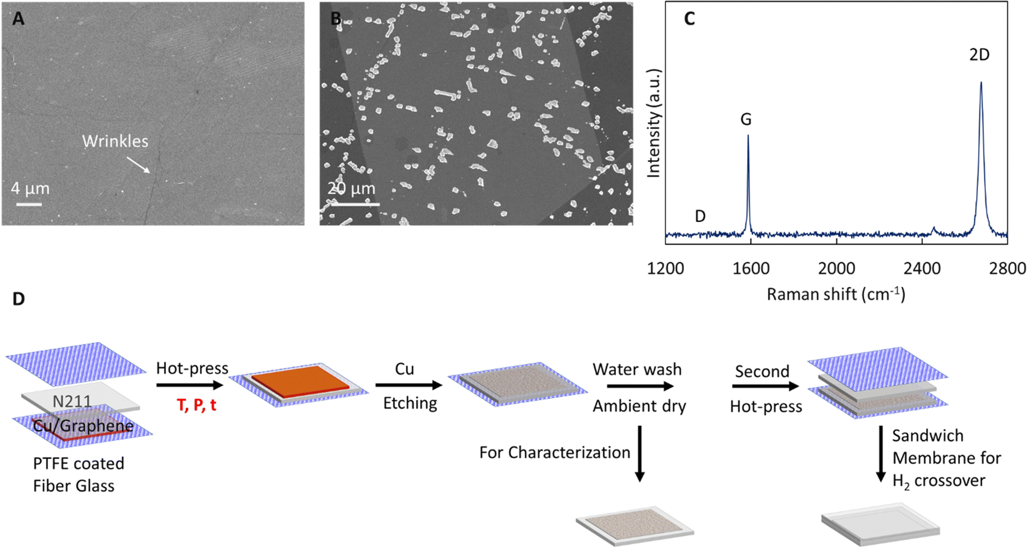 | ||
| Fig. 1 SEM image of (A) as synthesized graphene on Cu foil, and (B) etch pits on graphene|Cu after 5 s acid etch test with 0.1 M FeCl3. (C) Raman spectrum of graphene transferred onto 300 nm SiO2/Si substrate and (D) schematic of graphene transfer process to Nafion (N211). | ||
After the hot-press, the PTFE fiber sheet in the bottom side is carefully removed without disturbing the pressed graphene|Cu to obtain a PTFE|N211|graphene|Cu stack which is floated on 0.2 M APS solution to etch the Cu. After complete etching of Cu, the stack is floated on two separate DI water baths for 15 minutes each and dried under ambient conditions. The obtained N211|graphene was used for characterization of surface morphology of graphene transferred to N211 via SEM. Analysis (via thresholding using ImageJ software38) of spot like defects (formed likely via oxidation of Cu underneath defects in graphene) was performed on the Cu|graphene|Nafion stack. After Cu etching, the N211|graphene was pressed at ∼115 °C, ∼200 psi for 45 s against a second piece of N211 to prepare a sandwich Nafion|graphene|Nafion membrane. The sandwich membranes were soaked in 0.1 M HCl for 24 hours before testing. We note the actual temperature of the N211 during hot-pressing could be lower than the set temperature of the platens due to the presence of the Teflon sheets.
Measurement of proton transport
The N211|graphene|N211 sandwich membrane was used to measure proton transport as described in detail elsewhere.18 Pt/C (Pt loading 0.2 mg cm−2, fuel cell store) electrodes were used as anode and cathode and were hot-pressed at 140 °C for 1 min at 400 psi to the Nafion|graphene|Nafion sandwich membrane. The areal resistance was measured while supplying humidified H2 gas to both sides of the membrane via linear sweep voltammetry (LSV). The slope of the resulting I–V curve is equivalent to the membrane areal proton conductance and the inverse equal to the area specific resistance (ASR, after normalizing current to electrode area, ∼0.32 cm2). To measure the H2 crossover, the gas environment was changed to H2 and N2 on opposite sides of the membrane. The diffused H2 was measured as an oxidation current which is a measure of crossover across the membranes. The crossover current was reported at 0.4 V measured in 100% humidity at room temperature.Results and discussions
We initially assess the quality of the as synthesized monolayer graphene on Cu (see SEM image in Fig. 1A with wrinkles confirming graphene) via acid etch test (Fig. 1B) and Raman spectroscopy (Fig. 1C) after transfer to 300 nm SiO2/Si wafer. In acid etch test, FeCl3 permeates through defects in graphene and reacts with the underlying Cu substrate forming etch pits in the Cu foil which can be imaged with SEM to provide an indication of graphene quality.10 The total etched area of ∼7% is comparable to other prior reports for high quality graphene and the etch pits predominately seem to occur along wrinkles in the graphene.10,16,18,39 Next, Raman spectroscopy is used to probe the high crystalline quality of the synthesized graphene. The Raman spectra (Fig. 1C) shows the characteristic 2D (∼2700 cm−1) and G (∼1580 cm−1) peaks, an absence of the D-peak (∼1350 cm−1), I2D/IG >1, and 2D peak full width at half maxima (FWHM) < 30 cm−1, confirming high quality of the synthesized monolayer CVD graphene.40,41Having confirmed the high crystalline quality of the graphene, we proceed to systematically study parameters (see Table 1) influencing the transfer of graphene to a model proton conducting polymer Nafion (N211). We select hot-press as a facile and scalable process to achieve direct transfer of graphene to Nafion without the use of carrier layers and associated residues,21,34,36 and probe the influence of hot-press (i) time (t), (ii) temperature (T), and (iii) pressure (P).
| Temperature (°C) | Pressure (psi) | Time (s) | Defects features | Observations | |
|---|---|---|---|---|---|
| Ruptures | Spot like defects | ||||
| 140 | 600 | 120 | Optical images showed spot like defect features. Clustering of these spots appear similar to line like features or cracks in graphene and represent an intermediate between ruptures and spots. | Spot like defect features observed appear similar to etch pit formed upon acid etch of graphene on Cu, suggesting oxidation of Cu underneath defects in graphene causes further damage to graphene. | |
| 140 | 600 | 45 | |||
| 140 | 200 | 120 | Optical images showed spot like defect features. Clustering of these spots appear similar to line like features or cracks in graphene and represent an intermediate between ruptures and spots. No statistical difference seen in spot like defect features in optical images. | Spot like defect features seen in optical images. Not shown here. Temperature series for optimal t = 45 s is shown in Fig. 3 and analysis shown below within Table 1. | |
| 130 | 200 | 120 | |||
| 120 | 200 | 120 | |||
| 90 | 200 | 120 | Large patches of missing graphene layer (ruptures) observed. | Almost no spot like defect features observed. | SEM images showed large (several μm2) of missing graphene area in the form of large patches in the film (ruptures). Not shown here. |
| 50 | 200 | 120 | |||
| 140 | 200 | 45 | 4.49 ± 2.75% | 0.14 ± 0.35% | Analysis of SEM images is used to estimate area % of defects. Lower temperatures (<Topt) results in ruptures whereas high temperatures (>Topt) result in spot like defect features. |
| 115 | 200 | 45 | 0.38 ± 0.28% | 0.27 ± 0.09% | |
| 110 | 200 | 45 | 0.22 ± 0.09% | 2.27 ± 1.39% | |
| 90 | 200 | 45 | 0.43 ± 0.19% | 2.57 ± 0.11% | |
Initially, we probe the effect of hot-press time on graphene transfer to N211 and transfer graphene at hot-press conditions of 140 °C and 200 psi for two different hot-press times of 120 s and 45 s, as shown in Fig. 2A and B, respectively. Our rationale for choosing the highest temperature of hot-press ∼140 °C and the lowest pressure ∼200 psi in our study for the time dependence is to allow for clear observations by exacerbating effects that might not occur at lower temperatures as discussed further below. Optical microscopy images of the Cu|graphene|N211 surface shows dark spots (shown via arrows) for both conditions. However, with shorter hot-press time (45 s) the computed area of dark spots is significantly lower than 120 s (Fig. 2 and Table 1). The dark spots appear isolated for 45 s (Fig. 2A) in comparison to 120 s where the dark spots appear to coalesce into line like features (Fig. 2B and Table 1). ImageJ analysis of the % area of the dark spots are ∼0.5% for 45 s and ∼4% for 120 s, as shown in Fig. 2C, confirming longer press time results in higher dark spot like features. The density of the spots in Fig. 2B appear to be similar to the density of etch pits (Fig. 1B) and they also occur predominantly along wrinkles, as also observed for the acid etch test, suggesting these features originate from Cu oxidation underneath defects in CVD graphene on Cu foil. Hence, we propose oxidation of Cu underneath the graphene at elevated temperatures as a potential source for these dark spots. Such oxidation of Cu results in damage/holes in the CVD graphene and can also lead to poor transfer to Nafion due to non-uniformity of the surface.
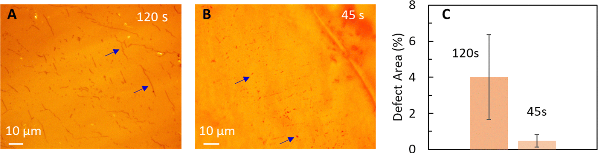 | ||
| Fig. 2 Optical images of graphene transferred to Nafion (N211) via hot-press (∼140 °C,∼200 psi) for (A) 120 s, and (B) 45 s. Blue arrows indicate spot like defects that correspond to damages in graphene via oxidation of Cu. Hot-press for longer duration leads to line like larger features (A and Table 1) corresponding to Cu oxidation and damage to graphene. (C) Comparison of % defect area for different hot-press times. | ||
Hence, we select 45 s as the duration of hot-press, P = 200 psi, and proceed to probe the influence of temperature on the quality of graphene transfer to Nafion. We specifically choose temperatures near the range of Tg values for Nafion in literature.42–44 In addition to optical microscopy images of Cu|graphene|N211 (Fig. 2A and B) we also used SEM to probe the surface morphology of the graphene transferred onto N211. Fig. 3A shows an SEM image of graphene transferred onto Nafion at T ∼140 °C with damages to graphene, specifically spot like defect features as well as clusters of spots resembling line like features.
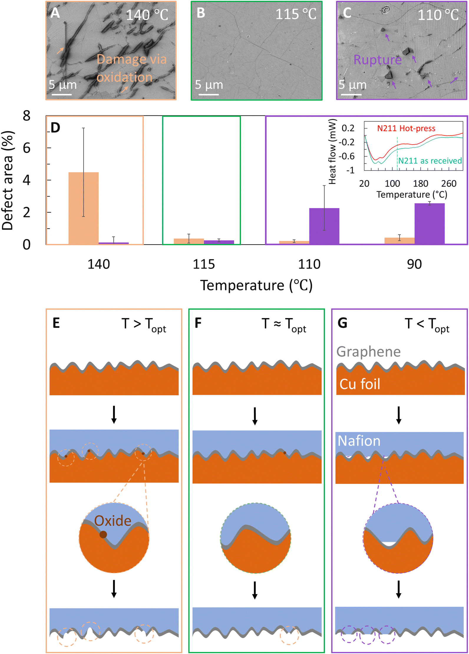 | ||
| Fig. 3 SEM images of graphene transferred to Nafion 211 at (A) 140 °C (>Topt), (B) 115 °C (∼ Topt) and (C) 110 °C (<Topt). At higher temperatures, spot like features similar to damage to graphene on Cu foil via oxidation of Cu underneath defects in graphene are observed (orange arrows in A). At lower temperatures, ruptured regions where graphene did not adhere to Nafion well are seen from the flipped over regions near edges (purple arrows). (D) Analysis of defective area attributed to oxidation (orange bars) and ruptures (purple bars) shows a trade-off in defect types with a minima ∼115 °C. Inset shows the DSC plots for as received and hot-pressed N211-H+ form membrane. A dotted line shows the Topt ∼115 °C which is near the end of the glass transition region of N211 polymer. Schematics of the graphene|Nafion interface (E) T > Topt, (F) T ∼ Topt and (G) T < Topt, where Topt is the optimum temperature of hot-press. When T > Topt, the Nafion conformally contacts the graphene surface. However, the high temperature tends to oxidize the Cu foil underneath defects in graphene (orange circles). At T < Topt, the Nafion does not make conformal contact (white patches) resulting in regions of patchy graphene transfer. Upon etching the Cu foil, these poorly-adhered regions tend to delaminate from the Nafion and are seen as a patch next to the ruptured area, as shown in (C). | ||
Although the overall transfer yield appears high with minimal patches of missing graphene, there appear to be features consistent with damage to the graphene film or defects (shown by arrows) covering ∼5% of the total area. The defect features resemble the shape and density of the dark spots observed in optical images shown in Fig. 2, confirming that the observed dark spots correspond to damage to the graphene transferred to N211 (Fig. 3A) and stem from oxidation of Cu underneath defects in graphene on Cu consistent with Fig. 2.
To mitigate the dark spots a series of transfers were performed at lower temperatures while keeping hot-press time ∼45 s and P ∼200 psi. Interestingly, upon lowering the temperature to T ∼115 °C (referred to as Topt) i.e. T ∼ Topt, the dark spot like defects account for <1% of the defective area (Fig. 3B). However, at lower temperatures T < Topt we also observe macroscopic ruptures in the graphene (Fig. 3C and Table 1). These ruptures are identified in SEM images as holes in graphene with bi-layer graphene regions around the edges. The ruptures originate from the apparent lack of adhesion of graphene to Nafion, which ‘flips over’ to form a bi-layer graphene area around the edges. With decreasing temperature, the percent area due to these ruptures increases up to ∼3% at 90 °C (Fig. 3D and Table 1). Since these features are not observed at temperatures above the Topt, we suspect they originate from non-conformal contact between the Nafion and the graphene/Cu surface (Fig. 3E–G). We note conformal contact between Nafion and graphene|Cu depends on the glass transition regime of Nafion. Hence, differential scanning calorimetry (DSC) studies were performed to understand the glass transition behaviour of Nafion (inset Fig. 3D).42–44 The onset of the glass transition regime is ∼60–70 °C, as indicated by the increased slope (inset Fig. 3D). The heat flow stabilizes at ∼125 °C, indicating the polymer has undergone a complete glass transition. This behaviour is similar to prior reports42–44 and attributed to the relaxation of the PTFE backbone of Nafion. The DSC curve yields a conventional glass transition temperature Tg ∼100 °C (taken as the midpoint between the onset and stabilized temperatures). Similar behaviour is observed for the sample which was hot pressed for 45 s at 115 °C. The minor differences in onset temperature point and heat flow for the as received N211 and hot-pressed Nafion are attributed to slight differences in sample weight, minor water loss and increased crystallinity of Nafion possible from hot-press. Based on the glass transition features of N211 and the observed optimum transfer of graphene on Nafion, Topt ∼ 115 °C corresponds to near complete glass transition of Nafion, resulting in improved conformal contact between Nafion and graphene|Cu (Fig. 3F).42–44
Above Topt, conformal contact between Nafion and graphene on Cu is possible, but the higher temperature leads to oxidation of Cu underneath the graphene that results in damages with dark spots and line like features (Fig. 3E), that are similar to etch pits in Fig. 2 (also see Table 1). In order to reach an intermediate trade-off between these two defect types, we transferred graphene at Topt ∼115 °C and indeed observed a minimum occurrence of both defect types. The schematics of graphene|Nafion interfaces are shown in Fig. 3E–G for different hot-press temperatures to emphasize the conformal contact between Nafion and graphene as well as oxidation features on copper.
Finally, for a comprehensive evaluation of hot-press parameters, we rationalize the low-pressure during graphene transfer on Nafion via hot-press at optimum condition of 115 °C (Fig. 3) and 45 s (Fig. 2). Fig. 4A and B show SEMs of graphene transferred at 200 psi and 1000 psi, respectively. An increase in ruptures in the graphene is observed at higher pressure which is likely due to combined effect of Cu metal deformation under load and compressibility of Nafion at high pressure (Fig. 4C and D).
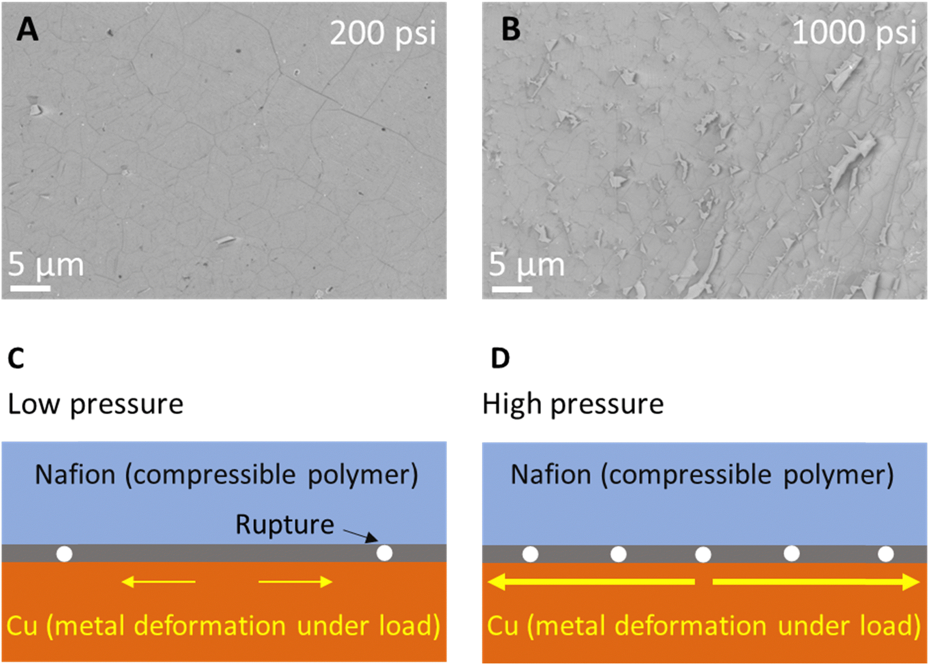 | ||
| Fig. 4 Graphene transfer on Nafion at 115 °C, hot-pressed at pressures (A) 200 psi, (B) 1000 psi for 45 s. (C) and (D) At higher pressure the ruptures in the transferred graphene increase due to increase in metal deformation of the Cu foil (note Cu is a soft and malleable metal which is subject to deformation/elongation under pressure). Such metal deformation results in ruptures to the graphene on Cu (see schematics). | ||
Using the optimized transfer conditions, we fabricated a Nafion|graphene|Nafion (N211|G|N211) sandwich membrane and evaluate the efficacy of the PEM by measuring proton transport and hydrogen crossover, respectively using a custom-built set-up (Fig. 5A). A schematic of the electrical connections and the membrane electrode assembly is shown in Fig. 5B. Fig. 5C, presents the I–V curves (obtained by feeding humidified H2 gas to both sides) for Nafion control membranes as well as N211|G|N211 sandwich membranes. The addition of graphene results in a marginal decrease in the measured current, indicating a marginal increase in the resistance (decrease in conductance) for protons (Fig. 5C and E). However, this marginal decrease in proton conductance with the addition of graphene is also accompanied by a substantial decrease in the hydrogen crossover current density (Fig. 5D). We note the transport mechanisms of protons and H2 gas (crossover) are different in Nafion. H2 transport primarily occurs in water channels in Nafion. Hence, an overlap of water channel pores in Nafion with macroscopic transfer defects in graphene will be necessary for H2 crossover to occur.
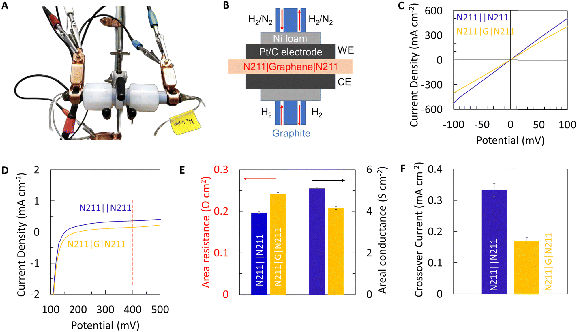 | ||
| Fig. 5 Gas phase proton transport measurements for PEM membrane-electrode assembly (MEAs) prepared via hot-press at 115 °C, 200 psi and 45 s. (A) Custom-built experimental set-up, (B) schematic of the MEA, (C) I–V plots with symmetric gas feed i.e. H2 gas on both sides of the MEA, (D) I–V plots exhibiting the hydrogen crossover current segment measured with H2 on one side and N2 gas feed on the other. (E) Area specific resistance (ASR) and areal conductance extracted from (C). (F) Crossover current density extracted from (D) at 0.4 V for N211||N211 control and N211|G|N211 membranes. | ||
The proton resistance for Nafion control and graphene sandwich membranes are extracted from the I–V plots (shown in Fig. 5C) using Ohms law and normalized to the membrane area ∼0.32 cm2 for area specific proton resistance (ASR). Fig. 5E, presents the area specific proton resistance for Nafion control membranes ∼0.19 Ω cm2 (areal conductance ∼5.1 S cm−2) and graphene sandwich membranes ∼0.24 Ω cm2 (areal conductance ∼4.2 S cm−2), respectively. Additionally, Fig. 5F shows the hydrogen crossover current (extracted from Fig. 5D) for Nafion control membranes (∼0.33 mA cm−2) and graphene sandwich membranes (∼0.17 mA cm−2) at 0.4 V at room temperature in a humidified environment. Notably, the graphene sandwich membranes fabricated using the optimal transfer process reduces the hydrogen crossover by ∼50%, while still maintaining ASR < 1 Ω cm2 (areal proton conductance > 1 S cm−2) adequate for enabling practical applications, thereby demonstrating the advantage of incorporating CVD graphene with Nafion for PEM applications.
Conclusions
To summarize, we systematically probed the influence of hot-press time, temperature and pressure for the direct transfer of CVD graphene onto Nafion. Our results indicate that hot-pressing for ∼120 s results in increased dark spot features that correspond to oxidation of Cu underneath defects in graphene compared to shorter time duration ∼45 s. The temperature of hot-press and its interplay with the glass transition temperature region of Nafion has a significant influence on graphene transfer. The optimum hot-press temperature, Topt ∼ 115 °C corresponds to near complete glass transformation of Nafion (glass transition temperature range 65–125 °C, Tg ∼100 °C). Transfers at T < Topt suffer from ruptures in graphene originating from lack of conformal contact between Nafion and graphene while T > Topt results in increased Cu oxidation related defects in graphene due to higher temperature. T ∼ Topt results in a minima for both ruptures and oxidation related defects in graphene. Finally, higher hot-press pressures resulted in significantly higher ruptures on graphene due to deformation of Cu, suggesting that low pressure is more suitable for graphene transfer on Nafion. Using the optimal transfer conditions, we fabricated Nafion|G|Nafion sandwich membranes that show ∼50% reduction in hydrogen crossover (∼0.17 mA cm−2) in comparison to Nafion control membranes (∼0.33 mA cm−2) while maintaining adequate ASR < 0.25 Ω cm2 (areal conductance ∼4–5 S cm−2) to enable practical PEM applications.Author contributions
P. R. K. conceived and supervised the project. P. C., N. K. M., T. K., and R. S. performed the transfers, characterization, and analysed the results. P. C., N. K. M, and P. R. K. wrote the manuscript with input and revisions from all authors.Conflicts of interest
P. R. K. acknowledges stake in a company aimed at commercializing 2D materials.Acknowledgements
The use of Vanderbilt Institute of Nanoscale Science and Engineering CORE facilities are acknowledged. This work was supported in part by NSF CAREER award #1944134, in part by DOE Early Career Research Program award # DE-SC0022915, in part by the U.S. Department of Energy Isotope Program, managed by the Office of Science for Isotope R&D and Production under award number DE-SC0022237. P. R. K. acknowledges the ECS Toyota Young Investigator Award. Part of this work was performed at the Center for Nanophase Materials Sciences at Oak Ridge National Laboratory, a U.S. Department of Energy Office of Science User Facility. Authors appreciate and acknowledge assistance from Dr. Aaron Daniel at the Department of Chemistry at Vanderbilt University for Differential Scanning Calorimetry measurements.Notes and references
- P. R. Kidambi, P. Chaturvedi and N. K. Moehring, Science, 2021, 374, eabd7687, DOI:10.1126/science.abd7687.
- S. Bukola, Z. Li, J. Zack, C. Antunes, C. Korzeniewski, G. Teeter, J. Blackburn and B. Pivovar, J. Energy Chem., 2021, 59, 419–430 CrossRef CAS.
- S. Hu, M. Lozada-Hidalgo, F. C. Wang, A. Mishchenko, F. Schedin, R. R. Nair, E. W. Hill, D. W. Boukhvalov, M. I. Katsnelson, R. A. W. Dryfe, I. V. Grigorieva, H. A. Wu and A. K. Geim, Nature, 2014, 516, 227–230 CrossRef CAS PubMed.
- J. S. Bunch, S. S. Verbridge, J. S. Alden, A. M. Van Der Zande, J. M. Parpia, H. G. Craighead and P. L. McEuen, Nano Lett., 2008, 8, 2458–2462 CrossRef CAS PubMed.
- H. Qi, Z. Li, Y. Tao, W. Zhao, K. Lin, Z. Ni, C. Jin, Y. Zhang, K. Bi and Y. Chen, Nanoscale, 2018, 10, 5350–5357 RSC.
- K. S. Novoselov, A. K. Geim, S. V. Morozov, D. Jiang, Y. Zhang, S. V. Dubonos, I. V. Grigorieva and A. A. Firsov, Science, 2004, 306, 666–669 CrossRef CAS PubMed.
- N. Metzger, I. Vlassiouk, S. Smirnov, G. Mariscal, R. Spragg and X. Li, J. Electrochem. Energy Convers. Storage, 2023, 20(2), 020903 CrossRef CAS.
- Q. Chen, Y. Y. Du, K. M. Li, H. F. Xiao, W. Wang and W. M. Zhang, Mater. Des., 2017, 113, 149–156 CrossRef CAS.
- M. Lozada-Hidalgo, S. Zhang, S. Hu, A. Esfandiar, I. V. Grigorieva and A. K. Geim, Nat. Commun., 2017, 8, 15215 CrossRef CAS PubMed.
- S. Bukola, Y. Liang, C. Korzeniewski, J. Harris and S. Creager, J. Am. Chem. Soc., 2018, 140, 1743–1752 CrossRef CAS PubMed.
- X. H. Yan, R. Wu, J. B. Xu, Z. Luo and T. S. Zhao, J. Power Sources, 2016, 311, 188–194 CrossRef CAS.
- S. M. Holmes, P. Balakrishnan, V. S. Kalangi, X. Zhang, M. Lozada-Hidalgo, P. M. Ajayan and R. R. Nair, Adv. Energy Mater., 2017, 7, 1601216 CrossRef.
- P. Chaturvedi, I. V. Vlassiouk, D. A. Cullen, A. J. Rondinone, N. V. Lavrik and S. N. Smirnov, ACS Nano, 2019, 13, 12109–12119 CrossRef CAS PubMed.
- M. I. Walker, P. Braeuninger-Weimer, R. S. Weatherup, S. Hofmann and U. F. Keyser, Appl. Phys. Lett., 2015, 107, 213104 CrossRef.
- J. L. Achtyl, R. R. Unocic, L. Xu, Y. Cai, M. Raju, W. Zhang, R. L. Sacci, I. V. Vlassiouk, P. F. Fulvio, P. Ganesh, D. J. Wesolowski, S. Dai, A. C. T. Van Duin, M. Neurock and F. M. Geiger, Nat. Commun., 2015, 6, 1–7 Search PubMed.
- P. Chaturvedi, N. K. Moehring, P. Cheng, I. Vlassiouk, M. S. H. Boutilier and P. R. Kidambi, J. Mater. Chem. A, 2022, 10, 19797–19810 RSC.
- S. Bukola, K. Beard, C. Korzeniewski, J. M. Harris and S. E. Creager, ACS Appl. Nano Mater., 2019, 2, 964–974 CrossRef CAS.
- N. K. Moehring, P. Chaturvedi, P. Cheng, W. Ko, A. P. Li, M. S. H. Boutilier and P. R. Kidambi, ACS Nano, 2022, 16, 16003–16018 CrossRef CAS PubMed.
- P. R. Kidambi, G. D. Nguyen, S. Zhang, Q. Chen, J. Kong, J. Warner, A. P. Li and R. Karnik, Adv. Mater., 2018, 30, 1804977 CrossRef PubMed.
- P. Cheng, F. Fornasiero, M. L. Jue, W. Ko, A. P. Li, J. C. Idrobo, M. S. H. Boutilier and P. R. Kidambi, Nat. Commun., 2022, 13, 1–12 Search PubMed.
- P. Cheng, M. M. Kelly, N. K. Moehring, W. Ko, A.-P. Li, J. C. Idrobo, M. S. H. Boutilier and P. R. Kidambi, Nano Lett., 2020, 20, 5951–5959 CrossRef CAS PubMed.
- S. Bukola and S. E. Creager, ECS Trans., 2019, 92, 439–444 CrossRef CAS.
- L. G. P. Martins, Y. Song, T. Zeng, M. S. Dresselhaus, J. Kong and P. T. Araujo, Proc. Natl. Acad. Sci. U. S. A., 2013, 110, 17762–17767 CrossRef CAS PubMed.
- S. Bae, H. Kim, Y. Lee, X. Xu, J.-S. Park, Y. Zheng, J. Balakrishnan, T. Lei, H. Ri Kim, Y. Il Song, Y.-J. Kim, K. S. Kim, B. Özyilmaz, J.-H. Ahn, B. H. Hong and S. Iijima, Nat. Nanotechnol., 2010, 5, 574–578 CrossRef CAS PubMed.
- S. J. Osborn, M. K. Hassan, G. M. Divoux, D. W. Rhoades, K. A. Mauritz and R. B. Moore, Macromolecules, 2007, 40, 3886–3890 CrossRef CAS.
- G. Calleja, A. Jourdan, B. Ameduri and J. P. Habas, Eur. Polym. J., 2013, 49, 2214–2222 CrossRef CAS.
- S. Yasuda, H. Matsushima, K. Harada, R. Tanii, T. O. Terasawa, M. Yano, H. Asaoka, J. S. Gueriba, W. A. Diño and K. Fukutani, ACS Nano, 2022, 16, 14362–14369 CrossRef CAS PubMed.
- S. M. Andersen, R. Dhiman, M. J. Larsen and E. Skou, Appl. Catal., B, 2015, 172–173, 82–90 CrossRef CAS.
- X. Wang, Y. Zhang, Y. Zhu, S. Lv, H. Ni, Y. Deng and Y. Yuan, Membranes, 2022, 12, 431 CrossRef CAS PubMed.
- I. Vlassiouk, M. Regmi, P. Fulvio, S. Dai, P. Datskos, G. Eres and S. Smirnov, ACS Nano, American Chemical Society, 2011, vol. 5, pp. 6069–6076 Search PubMed.
- I. Vlassiouk, P. Fulvio, H. Meyer, N. Lavrik, S. Dai, P. Datskos and S. Smirnov, Carbon, 2013, 54, 58–67 CrossRef CAS.
- S. Dhingra, J.-F. Hsu, I. Vlassiouk and B. D’Urso, Carbon, 2014, 69, 188–193 CrossRef CAS.
- P. R. Kidambi, C. Ducati, B. Dlubak, D. Gardiner, R. S. Weatherup, M. B. Martin, P. Seneor, H. Coles and S. Hofmann, J. Phys. Chem. C, 2012, 116, 22492–22501 CrossRef CAS.
- P. Cheng, J. Espano, A. Harkaway, A. E. Naclerio, N. K. Moehring, P. Braeuninger-Weimer and P. R. Kidambi, ACS Appl. Mater. Interfaces, 2022, 14, 41328–41336 CrossRef CAS PubMed.
- P. R. Kidambi, D. Jang, J. C. Idrobo, M. S. H. Boutilier, L. Wang, J. Kong and R. Karnik, Adv. Mater., 2017, 29, 1700277 CrossRef PubMed.
- P. Cheng, N. K. Moehring, J. C. Idrobo, I. N. Ivanov and P. R. Kidambi, Nanoscale, 2021, 13, 2825–2837 RSC.
- P. R. Kidambi, R. A. Terry, L. Wang, M. S. H. Boutilier, D. Jang, J. Kong and R. Karnik, Nanoscale, 2017, 9, 8496–8507 RSC.
- C. A. Schneider, W. S. Rasband and K. W. Eliceiri, Nat. Methods, 2012, 9, 671–675 CrossRef CAS PubMed.
- X. Xue, X. Chu, M. Zhang, F. Wei, C. Liang, J. Liang, J. Li, W. Cheng, K. Deng and W. Liu, ACS Appl. Mater. Interfaces, 2022, 14, 32360–32368 CrossRef CAS PubMed.
- A. Das, B. Chakraborty and A. K. Sood, Bull. Mater. Sci., 2008, 31, 579–584 CrossRef CAS.
- A. C. Ferrari and D. M. Basko, Nat. Nanotechnol., 2013, 8, 235–246 CrossRef CAS PubMed.
- S. H. De Almeida and Y. Kawano, J. Therm. Anal. Calorim., 1999, 58, 569–577 CrossRef CAS.
- Y. S. Kim, L. Dong, M. A. Hickner, T. E. Glass, V. Webb and J. E. McGrath, Macromolecules, 2003, 36, 6281–6285 CrossRef CAS.
- H. Y. Jung and J. W. Kim, Int. J. Hydrogen Energy, 2012, 37, 12580–12585 CrossRef CAS.
Footnote |
| † These authors contributed equally. |
| This journal is © The Royal Society of Chemistry 2023 |