
 Open Access Article
 This Open Access Article is licensed under a Creative Commons Attribution-Non Commercial 3.0 Unported Licence
Enhancing memristor fundamentals through instrumental characterization and understanding reliability issues
Fei
Qin
a,
Yuxuan
Zhang
a,
Han Wook
Song
b and
Sunghwan
Lee
 *a
*a
aSchool of Engineering Technology, Purdue University, West Lafayette, IN 47907, USA. E-mail: sunghlee@purdue.edu
bCenter for Mass and Related Quantities, Korea Research Institute of Standard and Science, Daejeon 34113, Republic of Korea
First published on 31st March 2023
Abstract
Memristors, a two-terminal device, have a resistance that can be changed and retained in two or more different states when subjected to electrical stresses. This unique function makes memristors now an attractive area of research for next-generation electronic devices such as memory and advanced computation. However, credible characterization methods for memristors are not fully established yet to understand fundamental working mechanisms and objectively evaluate figures of merit performance. This review encompasses various characterization methods from materials to electrical characteristics to identify the fundamentals of memristor operations. Meanwhile, large performance variation is the main bottleneck hindering the adoption of this class of devices in practical applications. Thus, the second part of this article focuses on the types of variation and other reliability issues of memristors. Possible strategies to enhance reliability are suggested as well. Topics covered in this review on memristors’ characterization techniques and reliability are of significant relevance to many studies that seek to advance the state of the art in electronic devices and systems towards neuromorphic computing.
 Fei Qin | Fei Qin is currently a PhD student in the School of Engineering Technology at Purdue University, under the supervision of Professor Sunghwan Lee. He received his Bachelor's degree in Applied Physics from Xi’an Jiaotong University and Master's degree in Physics from Temple University. His research primarily focuses on the design and optimization of memristors towards neuromorphic computing. |
 Yuxuan Zhang | Yuxuan Zhang received his Bachelor's and Master's degrees in Materials Science and Engineering from the University of Science and Technology Beijing in 2016 and 2019 respectively. He is currently a PhD student at the School of Engineering Technology at Purdue University, under the supervision of Professor Sunghwan Lee. His research primarily focuses on the design and optimization of electrode materials for high energy density Li-ion batteries. |
 Han Wook Song | Dr Han Wook Song is a Principal Research Scientist at Korea Research Institute of Standards and Science (KRISS) since 2006. He obtained his PhD degree in Materials Science and Engineering from KAIST in 2002. His research background includes the fabrication and characterization of thin film materials, especially piezoelectric materials for energy and sensing. His current research focuses on the establishment of national vacuum standards such as a quantum-based redefinition of vacuum. To this end, he evaluates and standardizes the pressure of objects through novel refractive index-based approaches. |
 Sunghwan Lee | Dr Sunghwan Lee is an Assistant Professor of Engineering Technology at Purdue University. He received his PhD degree in Materials Science and Engineering from Brown University in 2013. He completed postdoc training at MIT and Harvard University from 2013 to 2015. His current research pertains to the design and discovery of functional thin film materials to fundamentally understand the process–structure–property relationships. He is particularly interested in the engineering of defect structures, interfacial properties, and nanostructured materials with new functionalities for energy storage and conversion, transparent and flexible electronics, and sensing applications. |
1. Introduction
A memristor was proposed as a two-terminal electronic device by Leon Chua in 1971.1 It is a non-linear passive circuit element that can exhibit different resistance states, depending on the history of the voltage applied across its terminals. The first experimental demonstration of a memristor device was reported in 2008 by a research group led by R. Stanley Williams at Hewlett-Packard (HP) Laboratories.2–5 They used a thin film of titanium dioxide to create a memristor that exhibited the expected non-linear current–voltage characteristics and hysteresis behavior. After HP's experimental demonstration, several other teams around the world made significant efforts to independently reproduce the memristor behavior using different materials such as TaOx, HfOx, and InGaZnO.6–21 Then, research in memristors has gained significant attention due to the potential applications in various fields such as memory with a particular focus on higher-performance solid-state device technologies leveraging its binary switching behavior.22,23More recently, the synaptic switching behavior of memristors has been attracting increasing attention due to its potential applications in a variety of neural networks.24–26 Besides binary switching, the memristor's resistance can change continuously over a wide range of values, depending on the history of the pulse voltage applied across their terminals. This tunable multiple resistance level ability is crucial for neuromorphic computing because it can be used to adjust the weight of the connection between artificial neurons in a more precise and continuous way, to mimic the behavior of real synapses.27,28 Thus, memristors have been proposed as a key building block on the roadmap of neuromorphic computing and engineering.29
It is essential to understand the switching mechanisms of the memristor and measure the performance of the memristor by employing suitable characterization methods, which may require the exquisite design of testbeds and the non-trivial handling of materials and devices. From a material science of view, state-of-the-art, such as, transmission electron microscopy (TEM), X-ray photoelectron spectroscopy (XPS), and atomic force microscopy (AFM) are useful techniques to map and visualize the switching mechanisms and characterize the materials from each layer which in turn can provide experimental evidence of the switching behavior and insight for material selection and structure design. The mechanism for a memristor, in short, involves the movement of ions through a switching layer, causing a formation of conductive filament(s) (CFs). And TEM is a great technique to visualize this filament evolution, in the either planar or vertical structure of memristors. Also, the composition of the filament can be identified by further analysis with assistance from X-ray energy dispersive spectroscopy and electron diffraction. The chemical composition of the switching layer is a governing factor of the memristor performance. Especially, the switching behaviors of the valence change mechanism (VCM)-based memristors are driven by the change of the oxygen vacancy. With XPS characterization, one can examine the oxygen vacancy concentration of the fabricated switching layer, and then fine-tune and optimize the composition for better performance. The morphology of the memristor during the electrical stress is crucial information as well since it can degrade its performance. The surface distortions following electroforming and subsequent cycling between resistance states have been observed by XPS.
The electrical measurements are covered in this review, from DC sweeping to pulse measurements. DC sweeping is served as a starting point of the electrical characterization of a memristor. The memristive switching can be identified and endurance performance can be extracted. For fast testing and neuromorphic applications, pulse measurements are required essentially, thus, two pulse train profiles are selected and compared in this review for endurance and linearity characteristics. Advanced characterization of image processing which is to identify analog tuning accuracy is included as well. From an electro-chemistry perspective, cyclic voltammetry (CV) and electrochemical impedance spectroscopy (EIS) are also discussed for investigation on redox processes occurring prior to and during the switching events, respectively. This can provide valuable information for material selection and switching mechanisms. Detailed strategies and key achievements of each characterization method will be comprehensively discussed. Extensive studies have been reported on both single memristor devices and circuited devices with required structures such as crossbar arrays for practical applications such as neuromorphic computing hardware and random number generator.30,31 However, reliability, for example, the retention and endurance behavior of the memristors, has remained one of the fatal weaknesses which hinder their industrial adoptions in such applications. It is urgent to identify and categorize the metrics, symptoms, and solutions of memristors’ reliability issues. Thus, the second major part of this review is focused on typical reliability issues: cycling endurance, variation, retention, and nonlinearity. Less cycling endurance and retention directly shorten the lifetime of the functional memristors since the conductance levels are not distinguished anymore due to device degradation or failure. And larger order of variation, nonlinearity, and asymmetry cause accuracy loss during the processing of memristors’ operations. To identify and address these critical issues, possible mitigating strategies are covered and discussed. Density functional theory (DFT) and molecular dynamics (MD) calculations provide atomic- or molecular-level information that is not typically available from macroscale characterizations for examining the formation energy of defects, the energy barriers associated with ion migration, and the atomic-level dynamics of resistive switching. These calculations serve as valuable complements to instrumental characterizations.
To date, numerous review articles have been available, however, most of them are mainly review memristors by different materials selection (e.g., HfOx, TaOxetc.) or fascinating demonstrations of novel neuromorphic applications. It is rare to find reviews that focus both on characterization methods for a fundamental understanding of memristors’ behavior and directly intend to tackle one of the most major issues – reliability. Thus, we provide this review and further aim to fill the gap in this field. Since the memristors keep attracting attention, this review can pave the way and clean the blurry area for researchers and also be beneficial to the whole community to accelerate the development of memristors towards practical applications such as neuromorphic computing.
Part I. Characterizations for memristors
2. Transmission electron microscopy (TEM)
Transmission electron microscopy (TEM) is widely employed to obtain plan-view or cross-sectional images, featuring high-resolution microstructures, crystallographic information, and chemical elemental mapping often together with EDX.32–39 In addition, a wide range of in situ investigation capabilities are available in vacuum or environmental conditions, from which time-resolved evolution of materials structure and response to the stimuli such as temperature and bias can be recorded.40–42 Therefore, as a characterization approach to identifying materials and device behaviors for memristors, TEM is highly beneficial in not only ex situ structure analysis but also in visualizing the dynamic evolution of filaments in situ.43Fig. 1a and c show schematic illustrations of memristors with top electrodes (TE) and crossbar arrays, and Fig. 1b and d demonstrate corresponding cross sectional TEM images of these devices.21,44 Each layer of these memristors were clearly inspected and the uniform switching layers were identified. High-resolution (HR) TEM images associated with fast-Fourier-transform (FFT) diffraction patterns and EDX elemental analysis are instrumental to visualize the dynamic evolution process of conduction filament, through which the morphology, defect generation/annihilation, and composition are mapped in situ as well as ex situ. These capabilities of TEM have been leveraged to fundamentally understand and establish the switching mechanisms of memristors with vertical and planar configurations.32–37,45,46 Yang et al. contrived a SiO2-based planar memristor for TEM investigations where a novel TEM specimen (inset schematic of Fig. 1e) was devised with a ∼15 nm (lateral length) SiO2 switching layer sputtered on a 15 nm-thick SiNx low-stress membrane with an active electrode of Ag and an inert electrode of Pt.46 The thin SiNx membrane was employed to achieve a lower (brighter) background so that a higher contrast can be produced during TEM measurements. It should be noted that the planar design (memristor/TEM specimen) is unique in that the lateral structure can image the entire filaments, which is not available in vertical configurations and, hence, enables direct investigation of the evolution of filaments. In this ex situ measurements, the memristor was switched on and off in a separate controlled environment (i.e., before loading into the TEM chamber) and only exposed to high energy electrons during the imaging process, minimizing possible damages to the materials and device. Fig. 1e shows a plan-view TEM image of a pristine device, exhibiting the initial high resistance state (i.e., no filament formed) of the memristor. After applying a positive bias on the Ag electrode, filaments that completely and incompletely connect the two electrodes are recognized in Fig. 1f. With associated FFT analysis (Fig. 1h), the composition of the filaments was confirmed as Ag. Then, after a RESET process, both complete and incomplete filaments were dissolved from the switching layer/inert electrode (i.e., SiO2/Pt) interface, which is shown in Fig. 1g. The TEM images obtained from the main memristor states (initial, SET, RESET) convincingly suggest operation fundamentals of particularly ECM memristors, such as a self-limiting formation of filaments,47 which describes once a dominate filament is established, it reduces the electric field across the switching layer, in turn, restrains further formation of filaments, and the redox process of the EMC ions (i.e., Ag cations) at the inert electrode.48,49
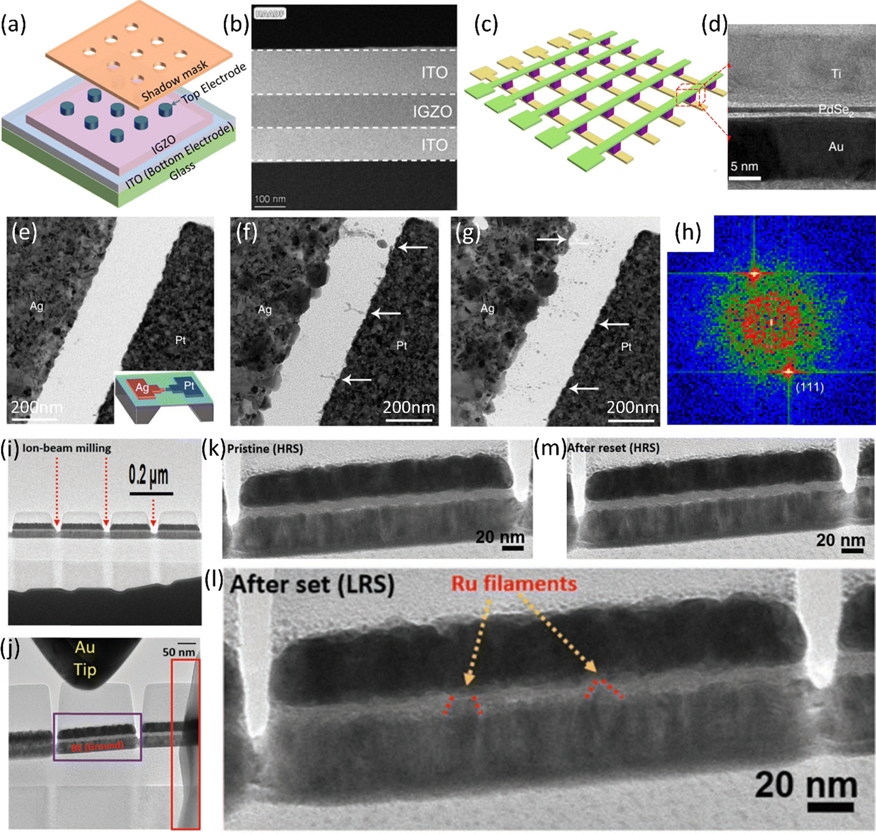 | ||
| Fig. 1 A demonstration of a typical two-terminal memristor: (a) schematic of typical vertical configuration memristors with top and bottom electrodes where the top electrodes define the memristor sizes and (b) its associated cross-sectional TEM image, presenting the device structure of ITO bottom electrode, IGZO switching layer, and ITO top electrode. Reproduced with permission from ref. 21. Copyright 2022, John Wiley and Sons, an example of a memristive crossbar: (c) schematic of crossbar arrays of memristors and (d) its cross-sectional TEM image, showing the vertical structure of a single memristor (Ti/PdSe/Au) from the arrays. Reproduced with permission from ref. 44. Copyright 2021, Springer Nature, observation of conductive filaments in a planar memristor by TEM: a TEM image of a pristine SiO2-based planar memristor. (f) After the first-time turn-on process, a TEM image was captured to visualize the complete and incomplete filaments. (g) After RESET process, the TEM image shows that all filaments were dissolved. (h) FFT results of the HRTEM image of an Ag nanoparticle in the filament of the switching layer, which indicates Ag (111) was identified. Reproduced with permission from ref. 46. Copyright 2012, Springer Nature, TEM examination on conductive filaments evolution in a vertical memristor: (i) bright-field TEM image of nanopillar shape samples for TEM imaging by ion-beam milling. (j) Setup to apply bias through a probe tip on the Pt(top)/Ta2O5/Ru(bottom) memristor for in situ TEM investigation. Cross-sectional in situ TEM images of (k) the pristine state (HRS), (l) after SET state (LRS) where two conductive filaments are observed, and (m) after RESET, back to HRS. Reproduced with permission from ref. 50. Copyright 2020, John Wiley and Sons. | ||
TEM examinations from vertically stacked memristors were also demonstrated, by which the formation/rupture of the conduction filament was imaged from more typical device structures. Fig. 1i shows a cross-sectional TEM image of Ta2O5-based memristors individualized by applying focused ion beam (FIB) to vertically deposited Pt/Ta2O5/Ru layers.50 The thickness of sputtered switching layer Ta2O5 was only 5 nm to make it electron transparent which is beneficial for TEM observation. The bottom Ru layer is continuous (not divided by FIB), thus, bottom electrodes of all nanopillar memristors by FIB are connected to each other and also connected to the bottom contact for grounding, which is highlighted with an empty red square in Fig. 1j. And the examination sample was loaded to a nano-biasing holder. To make a good contact between the probe and carbon-coated Pt top electrode, a sharpen and flexible gold tip was employed. A clear sandwich structure with a uniform 5 nm Ta2O5 switching layer was identified in the Fig. 1k for the initial state of the device. After a SET process, i.e., a negative bias was applied on the Pt through the Au tip, two distinguishable Ru filaments were able to be observed in Fig. 1l. The Ru filaments yielded by the migration and accumulation of Ru were identified with ex situ EDX analysis, indicating a low resistance state established. Afterwards, with a RESET process by applying a positive through the Au tip, the Ru filaments were dissolved and generated a high resistance state which is presented in Fig. 1m.
From these studies of in situ and ex situ TEM investigations, the fundamental memristor switching mechanisms involving the formation and rupture of conduction filaments were visually identified at the nanoscale. Therefore, TEM is a powerful technique to characterize the device structure, more importantly, the morphology and composition of conductive filaments evolution which can reveal the switching mechanism definitively.
3. X-Ray photoelectron spectroscopy (XPS)
X-Ray photoelectron spectroscopy (XPS) offers a high-resolution identification of chemical environment of elements within a material, valence states, and electronic structures.51,52 Due to these capabilities, XPS has been utilized in memristor applications to identify the chemical composition, doping states and functional bonding of the memristor components (i.e., switching layer and electrodes).53–63 Therefore, XPS is instrumental to analyze the major factors which control the evolution of the filaments and hence enhance the fundamentals of the switching mechanisms.With a TaOx-based memristive crossbar, Kim et al. demonstrated a functionally complete three-valued Łukasiewicz logic system, which describes a multivalued logic for enhancing the computing efficiency by reducing the data size.64 At the single device level, the oxygen content in each oxide layer of a bilayered tantalum oxide-based memristor was modulated by adjusting the partial pressure of O2 during the deposition. Through XPS, the valence state of Ta and the oxygen deficiency were identified to understand their effect of the chemical environment on the memristor behavior. The structure of the bilayered memristor is schematically shown in Fig. 2a where the ‘x−’ and ‘x+’ represent that TaOx− is more oxygen-deficient than TaOx+. And this oxygen content differentiation was confirmed by the high resolution (HR) XPS analysis of the Ta 4f spectra in Fig. 2b, indicating both layers were oxygen-deficient and quantitatively x− = ≈1.6 and x+ = ≈1.9, in reference to the stoichiometric phase, Ta2O5. The bottom table in Fig. 2b summarizes the atomic percentage of each valence state of Ta in the bilayers. The O 1s HR spectra for both layers were examined and depicted in Fig. 2c. The blue peak, which is located at 530 eV and referred to as OI, and the green peak, which is located at 531 eV and referred to as OII, are associated with the bonding of Ta and O in a stoichiometric Ta2O5 and oxygen-deficient tantalum oxide, respectively. The ratio of the area of OI (blue) to OII (green) is 3.57 in TaOx− and 5.0 in TaOx±, validating that TaOx− is more oxygen-deficient, aligning with the results of the Ta 4f spectra. With the optimized oxygen content, the bilayered tantalum oxide-based memristor operates in three distinct states: LRS, HRS, and an intermediate resistance state (IRS). Fig. 2d shows the retention characteristics for these states, and they are stable enough to demonstrate the potential application for a logic system representing ternary states. The switching mechanism from oxygen concentration-modulated TaOx−/TaOx+ was proposed as in Fig. 2e where blue dots represent oxygen vacancies and each state with oxygen vacancy distribution is illustrated. Comparing with TaOx+, the oxygen-vacancy concentration is higher in the TaOx− layer in the pristine state. The first SET (i.e., forming) process yielded a conical shape conductive filament and it has wider width in the TaOx−, and only the thinner (weaker) filament in TaOx+ was dissolved during the first RESET process. With the second RESET process, the wider (stronger) filament in TaOx− was destroyed as well, leading to HRS. Then, only TaOx− filament was recovered by a SET process due to a larger oxygen vacancy concentration in TaOx− layer, creating the IRS. An additional SET is needed to extend the filament to TaOx+ for LRS.
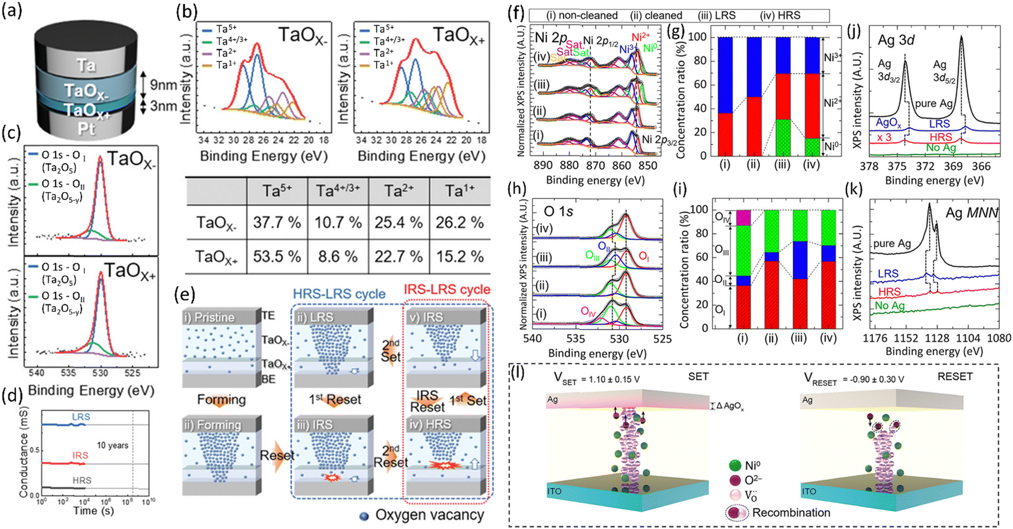 | ||
| Fig. 2 XPS analyses for optimizing compositions of the switching layer and identifying the switching mechanisms. Bilayer TaOx-based memristors: (a) the structure of a bilayer tantalum oxide memristor. (b) Core-level HR Ta 4f XPS with peak fittings of each tantalum oxide layer and associated atomic percentage. The table summarizes the atomic percentage of each peak estimated from the HR XPS analyses. (c) XPS O 1s peak fittings of tantalum oxide layers. (d) Retention measurements at the three resistance states (RLRS, RIRS, and RHRS) of the bilayer tantalum oxide memristor (e) schematic illustration of the switching mechanism of the bilayer tantalum oxide-based memristor, describing LRS, HRS and IRS. Reproduced with permission from ref. 64. Copyright 2021, published by John Wiley and Sons. This is an open access article distributed under the terms of the Creative Commons CC BY license, and NiOx-based memristor: XPS spectra of (f) Ni 2p core level and (h) O 1s core level and the associated valence-state concentration ratio in (g and i), respectively. (j) Ag 3d core level XPS spectra of pure Ag (TE), both LRS and HRS states with a control condition (i.e., no Ag). (k) Associated Auger spectra of Ag MNN. (l) Proposed switching mechanism of NiOx-based memristor based on the XPS analysis. Reproduced with permission from ref. 39. Copyright 2022, American Chemical Society. | ||
XPS may enable one to investigate chemical content variation for each switching stage, through which the switching mechanism of a memristor can be established. Park et al. reported such an investigation on NiOx-based memristors.39 XPS analyses were carried out for the four following cases: (i) non-cleaned NiOx, (ii) cleaned (by ion beam) NiOx, (iii) NiOx at LRS, and (iv) NiOx at HRS. Fig. 2f exhibits the Ni 2p core levels XPS data for the four cases, where green Ni0 peaks are only observable in the case (iii) LRS and (iv) HRS, indicating a shift in the Ni 2p peaks. Fig. 2g compares the concentration ratios of Ni3+, Ni2+, and Ni0 in the four cases. And it shows that a significant change in concentration ratios of Ni2+ and Ni0 occurred in (iii) LRS and (iv) HRS, whereas Ni3+ remained stable due to a stronger Ni3+–O bond. Thus, oxygen vacancies were formed around Ni2+ ions in LRS. O 1s core levels XPS spectra for four cases are plotted in Fig. 2h. The pink OIV peak at 532.4 eV indicates the presence of weak binding and/or interstitial oxygen and surface hydroxyl groups, i.e., NiO(OH), Ni3+ state, and OIV peak can be perceived only in case (i) pristine NiOx. The NiOx film was cleaned in case (ii) with an Ar+ ion beam to remove chemical adsorption on the NiOx surface, resulting in a removal of the OIV peak. Peaks of OI, and OIII are related to oxygen lattice, oxygen vacancy, and non-lattice, respectively. According to Fig. 2i, from (iii) LRS to (iv) HRS, the oxygen-vacancy (OII) concentration decreased from 31.7% to 13.5%, while OIII was barely changed, similarly due to the strong bonding of Ni3+–O. In case (iv) HRS, the O2− ions repopulate the original lattice position of the NiOx, leading to a decrease in oxygen vacancy. In contrast, in case (iii) LRS, Ni2+ is reduced to Ni0. The XPS analysis was used to estimate the Ni and O composition ratios for cases (ii) to (iv). In case (ii), the Ni and O composition ratio was determined to be 1![[thin space (1/6-em)]](https://www.rsc.org/images/entities/char_2009.gif) :1.3 without the presence of Ni0. After the forming process, this ratio shifted to 1:0.9 in case (iii) LRS and 1:1.2 in case (iv) HRS when Ni0 was present. This quantitative analysis implies that the digital bipolar switching behavior of the NiOx-based memristor is related to the valence change mechanism (VCM), which is influenced by changes in the oxygen vacancy within the NiOx layer. With further analyses of Ag 3d3/2 and Ag 3d5/2 core levels XPS spectra in Fig. 2j and associated Auger spectra of Ag MNN in Fig. 2k, the authors claimed the bipolar switching behavior arises from various electrochemical reactions at the Ag/NiOx interface, involving Ag and AgOx, and within the NiOx layer, involving Ni2+ and Ni. The switching mechanism of the Ag/NiOx/ITO memristor can be demonstrated based on the XPS analysis, as depicted in Fig. 2l. When SET voltage is applied to the Ag top electrode, the O2− ions from the NiOx layer are able to easily move into the Ag electrode, which results in the separation of the O2− ions from the oxygen lattice sites, or the drift of oxygen vacancy. The partial O2− ions from NiOx then gather at the Ag/NiOx interface, leading to the formation of AgOx (left side of Fig. 2l). In the NiOx layer, the conductive filament can be established between Ag/AgOx and ITO, switching the device to its LRS. On the other hand, when a RESET voltage is applied to the Ag top electrode, the O2− ions from AgOx are replenished back to the NiOx layer, partially neutralizing and recombining with oxygen vacancy (right side of Fig. 2l). This process can lead to the partial rupturing of the filament near the Ag top electrode, switching the device to its HRS.
:1.3 without the presence of Ni0. After the forming process, this ratio shifted to 1:0.9 in case (iii) LRS and 1:1.2 in case (iv) HRS when Ni0 was present. This quantitative analysis implies that the digital bipolar switching behavior of the NiOx-based memristor is related to the valence change mechanism (VCM), which is influenced by changes in the oxygen vacancy within the NiOx layer. With further analyses of Ag 3d3/2 and Ag 3d5/2 core levels XPS spectra in Fig. 2j and associated Auger spectra of Ag MNN in Fig. 2k, the authors claimed the bipolar switching behavior arises from various electrochemical reactions at the Ag/NiOx interface, involving Ag and AgOx, and within the NiOx layer, involving Ni2+ and Ni. The switching mechanism of the Ag/NiOx/ITO memristor can be demonstrated based on the XPS analysis, as depicted in Fig. 2l. When SET voltage is applied to the Ag top electrode, the O2− ions from the NiOx layer are able to easily move into the Ag electrode, which results in the separation of the O2− ions from the oxygen lattice sites, or the drift of oxygen vacancy. The partial O2− ions from NiOx then gather at the Ag/NiOx interface, leading to the formation of AgOx (left side of Fig. 2l). In the NiOx layer, the conductive filament can be established between Ag/AgOx and ITO, switching the device to its LRS. On the other hand, when a RESET voltage is applied to the Ag top electrode, the O2− ions from AgOx are replenished back to the NiOx layer, partially neutralizing and recombining with oxygen vacancy (right side of Fig. 2l). This process can lead to the partial rupturing of the filament near the Ag top electrode, switching the device to its HRS.
4. Atomic force microscopy (AFM)
Atomic force microscopy (AFM) is a technique used to measure not only the typical surface topography and mechanical properties but also electrical response, electronic structures (e.g., work function), and electrochemical behavior of materials at the nanoscale.65–73 It works by scanning a very sharp probe over the surface of a sample, and measuring the various signals between the probe and the surface. By plotting these signals as a function of the probe's position, an AFM can produce a detailed map of such informative properties to understand the nature of materials.74In addition to these various capabilities, it is further promising for memristor characterizations that AFM can identify the changes that occurred in these properties during the operation of the memristor. This information can be used to understand the mechanisms by which memristors function, and to optimize their performance.75,76 For example, AFM can be used to measure the resistance of a memristor as a function of applied bias through, known as conductive AFM (C-AFM or current mapping), which can provide insights into the mechanisms underlying the device's resistive switching behavior.77 AFM can also identify the effect of the surface roughness and roughness distribution of the materials on the memristor performance.78
Sun et al. used the current mapping method on CH3NH3PbI3 (MAPbI3)-based memristors to investigate the switching mechanism.79 The tip of C-AFM was coated with Pt and served as a grounded top electrode, and Fluorine-doped Tin Oxide (FTO) is the bottom electrode where a bias voltage is applied (i.e., Pt/MAPbl3/FTO structure). The measurement is schematically described in Fig. 3a. The large bias voltage is applied to the upper part of the sample only. After the upper scanning, a full scan is carried out on the whole area of the sample with a small voltage, basically this is a read process. Fig. 3b shows the current mapping for a −8 V upper scanning and Fig. 3c presents a 0.5 V full read mapping. At another area with the same size, a +8 V upper scanning and 0.5 V full read process were completed and associated current mapping images are displayed in Fig. 3d and e. The areas were divided into high-bias scanned (high current level) and non-scanned (low current level) parts for both −8 V and +8 V cases. These results indicate that the MAPbI3 functioning layer can be turned on to LRS in both bias directions, which suggests that the resistive switching relies on its own defects of MAPbI3 film due to the fact that if the switching relies on ions from a specific electrode, only one biasing direction (i.e., to the specific electrode) should turn on the device. Also, an interesting phenomenon can be observed by comparing Fig. 3c and e that −8 V SET has a sharp edge between scanned and non-scanned parts and +8 V SET has an indistinct boundary, implying −8 V SET process is more complete than +8 V. This bias dependent behavior is attributed to that the area of the Pt-coated tip is smaller than the bottom electrode, causing an asymmetrical bipolar resistive switching.
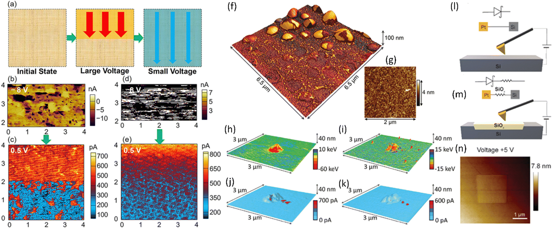 | ||
| Fig. 3 C-AFM investigation on switching mechanism of MAPbI3-based memristor: (a) diagram of C-AFM measurement procedure, where a large voltage scan is carried out only at the upper part of the square area, and then a low voltage read process is scanned on the entire area. Current mapping images of a MAPbI3/FTO structure with voltage bias of (b) −8 V, (d) +8 V for stressing in the upper area, and (c and e) 0.5 V for corresponding read processes for both biases. Reproduced with permission from ref. 79. Copyright 2018, American Chemical Society. AFM examination on SiO2-based memristor: (f) AFM topography of the surface of the switching layer SiO2 after initial bias applied and (g) its pristine counterpart image. Energy dissipation mapping images obtained with (h) a positive-bias initial stressing and (i) a negative one. Associated C-AFM conductivity mapping for (j) positive stressing and (k) negative one. Reproduced with permission from ref. 80. Copyright 2016, published by John Wiley and Sons. This is an open access article distributed under the terms of the Creative Commons CC BY license. In situ fabrication and investigation of SiOx-based memristors directly on Si formed by C-AFM: diagrams for CAFM tip-induced oxidation (l) set up and (m) establishment. (n) Topography of silicon oxide hillocks on Si surface formed by applying 8 min +5 V bias scan. Reproduced with permission from ref. 81. Copyright 2022, American Chemical Society. | ||
Mehonic et al. investigated the surface distortion of switching layer after bias applied through AFM in tapping mode.80 In order to eliminate the need for removing the upper electrode from a specimen after undergoing electrical stress, the SiOx switching layer was directly subjected to bias via a conductive probe, i.e., served as a top electrode. Voltage pulses of either +20 V or −20 V were applied at different locations, thus enabling examination on the effects of both positive and negative biases. As shown in Fig. 3f, bubble-like features with diameters ranging up to hundreds of nanometers were commonly observed in the vicinity of the probe contact point. As comparison, Fig. 3g is the topography image of pristine SiOx, exhibiting highly flat surface with a 0.2 nm root-mean-square roughness. In some instances, permanent bumps were noticed at the bias point after undergoing electrical stress, these bumps were up to a few hundred nanometers in width and approximately 40 nanometers in height. The energy dissipation mapping can reveal material's mechanical properties such Young's modulus. Thus, the scans of energy dissipation are shown in Fig. 3h for positive bias and Fig. 3i for negative bias. These energy dissipation results suggest that the conductive region is less stiff than the pristine area. Elevated areas were found to dissipate more energy than the original surface under both positive and negative stress. Conversely, some regions demonstrated lower energy dissipation, indicating localized hardening. C-AFM reveals a correlation between surface distortion and areas of elevated conductivity (as demonstrated in Fig. 3j and k). It can be inferred that both positive and negative biases cause an expansion of the oxide layer, which is accompanied by an increase in local conductivity. This implies that Joule heating caused by the flow of current leads to a distortion in the local structure, resulting in surface deformation and regions of varying hardness.80
In addition to the surface, electrical and mechanical characterizations for memristor applications, AFM can also form an oxide switching layer directly from a metal species (then becomes a bottom electrode). Peiris et al. grew silicon oxide hillocks on Si surfaces by C-AFM tip-induced oxidation to fabricate a silica based memristor.81 The thickness of oxide film was controlled by the magnitude of the applied bias, duration polarity and the Si doping type, i.e., n-type and p-type. Fig. 3l demonstrates the process set up schematically where a positive bias is applied on n-type Si. Fig. 3m pictorially describes an AFM tip-induced silicon oxide hillock is established. For example, with an 8 min +5 V bias scan, the average height for the AFM tip-induced oxide achieved 6.3 ± 0.37 nm, as shown in Fig. 3n. And this kind of AFM tip-induced memristor shows an on/off ratio larger than 104.
5. I–V DC sweeping
In this section, DC sweep measurements will be reviewed as a typical electrical evaluation of memristors, which can also serve as a great starting point for learning the resistive switching behavior and associated mechanism. Fig. 4a describes a typical I–V curve for the most studied bipolar filamentary memristor. The top electrode is connected to the electrical bias and the bottom electrode is grounded. Thus, the ramped voltage stresses are added across the switching layer of the memristor. An as-prepared (or un-biased) memristor is initially in the high resistance state (HRS), or OFF state which can be considered as logic value ‘0’. With an application of the positive external electrical stress, a formation of conductive filament in the switching layer and the memristor is switched to a low resistance state (LRS), or ON state which can be considered as logic value ‘1’. This process is referred to as the ‘SET’ process, and the voltage ignited the transition is called SET voltage (Vset). After reaching the LRS, the positive voltage is reduced to 0, and increase negatively to enable another transition. At certain negative bias, a RESET voltage (Vreset), the conductive filament is ruptured, and the LRS of the memristor is switched back to initial HRS, i.e., a RESET process is established. During the forward and backward sweeps, the current values are checked at the same voltage, typically ∼0.1 V, which turns out that there is a gap between these two current levels. This current checking is called “read”, and the resistances (RHRS and RLRS) at two states can be simply calculated with the read voltage (∼0.1 V) and current values. It is worth noting that a limited current (compliance current) was usually employed during the DC sweeping for collecting hysteretic I–V curves. And the compliance current can prevent an irreversible hard break on the memristor.82–84Fig. 4b presents one cycle of I–V sweeping characteristics in linear scale of an Ag/HfO2/Pt memristor with associated schematic elucidation of its switching mechanism.85 It clearly introduces the relations between the electrochemical processes and each switching state in the electrical characteristics. With a positive bias, the top electrode, chemically active Ag, is partially oxidized as Ag+ ions. And then, these Ag+ ions migrate towards the bottom noble Pt, and are reduced to Ag atoms there. The accumulated Ag atoms form conductive filaments across the dielectric layer and a SET process is completed. Thus, in the LRS, the memristor exhibits an ohmic transport mechanism. When a negative bias is applied to the top Ag electrode, the oxidation of Ag filaments into Ag+ ions and reduction at the Ag electrode reversibly occurred, which led to the rupture of the filament conduction path and switching these devices to an OFF state (RESET process). DC sweeping I–V evaluation is often plotted as the logarithm of currents’ absolute values vs. linear voltage values which is called semi-log or butterfly graph. In this way, the RLRS/RHRS ratio is visualized much more clearly. Fig. 4c is a semi-log presentation of the measurement for a SiO2/Ta2O5 based memristor.86 1000 cycles of DC sweeping data are all plotted in the butterfly graph. The plot commonly shows the variation of each cycle, it is reasonable to highlight typical cycles, such as the first and last cycle, as Fig. 4c does, or the average/fit of all cycles. Fig. 4d summarizes the distribution of resistance values of SiO2/Ta2O5 based memristor at HRS and LRS along with the cycle number, i.e., endurance behavior, which is extracted from I–V measurements at 0.1 V. The endurance characterization visualizes the on/off ratio, switching variation, and cycling number during the repeated DC sweeping in a more quantitative way. When the semi-log and endurance characteristics are reported, the data in very cycle should be included, especially, only 100 cycles are presented for DC sweeping commonly. It should be noted that measured RHRS and RLRS in each cycle should be all reported. If one uses only one data point to present 10 cycles of data, it is possible that some failure cycles occur within 10 cycles, thus, the endurance is overestimated. This issue is also noticed in another article, and the authors argued that measuring and reporting endurance for every cycle is especially important for advanced materials (e.g., 2D materials, perovskites, MXenes)87–92 based memristors and nanostructured (e.g., nanowires and nanotubes)93–96 memristors as their switching mechanisms and their reliability have not been demonstrated by other groups and not been established.97 Therefore, the performance of these devices requires further objective evaluations as the performance since related mechanisms are controversial and not widely accepted. The DC sweeping data can be interpreted in double logarithm scale to analyze the conduction mechanisms.98 For example, in the Fig. 4e, the DC sweeping current–voltage curves from an Ag/ZnO/ITO memristor was plotted in double logarithmic coordinates during the SET process.99 During initial HRS within low positive bias region, the current flowing shows a linear relationship (I ∝ V, i.e., the slope is around 1) indicating an ohmic conduction mechanism, corresponding to thermally generated carriers. Along with an increasing bias, the slope of the current–voltage curve increases to 1.9, i.e., I ∝ V2, which implies that the current flowing follows a space charge limit current (SCLC) conduction mechanism before the HRS/LRS transition.99,100 When Ag filaments were formed, the memristor transitioned to LRS and the slope became 1 again, followed Ohm's law. Although the DC sweeping is a basic characterization for memristor, this measurement can reveal key information such as endurance, variation and conduction mechanism with different interpretations.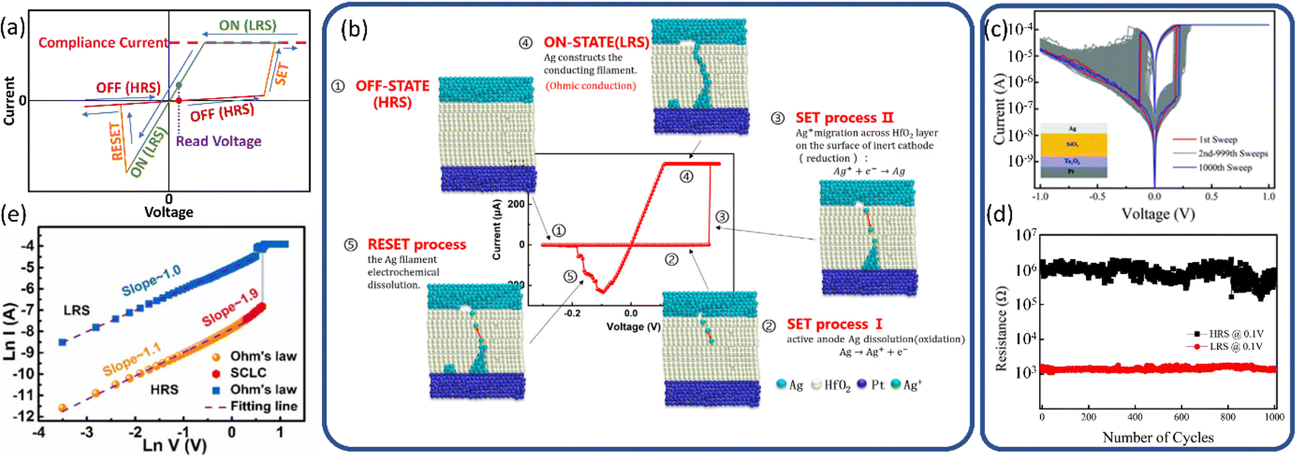 | ||
| Fig. 4 Elaboration of DC sweeping I–V characterization. (a) A detailed explanation of a typical I–V curve in linear–linear scale from DC sweeping, indicating bipolar resistive switching. (b) Actual DC sweeping I–V characteristics and corresponding switching mechanism of an Ag/HfO2/Pt memristor. Reproduced with permission from ref. 85. Copyright 2018, published by MDPI. This article is an open access article distributed under the terms and conditions of the Creative Commons Attribution (CC BY) license, a SiO2/Ta2O5 based memristor, showcasing (c) 1000 cycles of DC sweeping data plotted in semi-log scale (linear scale x-axis and log scale y-axis). The curves of all cycles are displayed and the first and last cycles are highlighted. (d) Associated endurance characteristics obtained from resistance values read at 0.1 V at HRS and LRS. Reproduced with permission from ref. 86. Copyright 2020, The Royal Society of Chemistry, and (e) Double-log scale analysis for an Ag/ZnO/ITO memristor, where the slopes of HRS and LRS determine the α value in the I ∝ Vα, indicating the conduction mechanism. Reproduced with permission from ref. 99. Copyright 2021, Elsevier. | ||
6. Pulse
As reviewed in the previous section, a variety of information can be retrieved by utilizing DC sweeping characterization. However, the slow DC ramping may be not suitable for most of the practical electronics applications. Lanza et al. claimed that if the memristor device fails to switch within 1 microsecond, it becomes not useful for the majority of resistance switching technologies.97 In addition, many reports claim that 106 or higher endurance performance, thus, through time-consuming DC sweeping is not a realistic approach for measuring such a high number of switching cycles.101–107Pulse measurements are instrumental to address these issues Fig. 5a is a typical endurance characteristics plot employing the pulse technique, obtained from cellulose nanocrystal (CNC)-based memristor.108 The x-axis represents the pulse number and y-axis is labeled for resistance, or other equivalent information such as current, or conductance. A typical scheme of a pulse train for endurance characterization is shown in Fig. 5b, which includes the cycle as follows: a READ pulse, a SET pulse, a READ pulse, a RESET pulse, and a READ pulse.97 And sufficient number of data points is also crucial since insufficient data points (i.e., with low resolution) may not be able to identify the SET/RESET behaviors. In Fig. 5b, the SET/RESET processes are exampled with the adequately large number of points, showing detailed switching behaviors. However, a large volume of data often limits obtaining pulse measurements beyond a certain number of data points. Therefore, optimizing the size of data while being able to demonstrate the performance profile is required. Despite the practical usefulness of pulse measurements as a memristor characterization, we notice two major issues. First, READ pulse is missing in the pulse scheme. Second, the result does not report all the resistance values for the whole cycling test. These data exhibitions are not recommended.
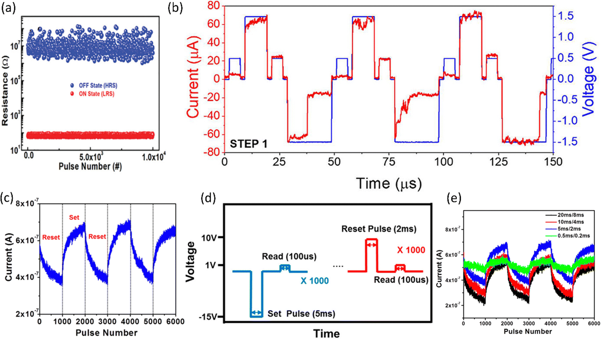 | ||
| Fig. 5 Demonstration of pulse measurements for endurance and linearity characterization. A typical endurance characteristic of a memristor with a pulse, enabling a large number of cycling: (a) a pulse-measured endurance characteristics of a cellulose nanocrystal (CNC)-based memristor with 104 pulse cycles. Reproduced with permission from ref. 108. Copyright 2021, John Wiley and Sons, (b) a segment of pulse endurance characteristics. A blue pattern represents the applied pulse scheme and a red pattern provides the recorded current values. The smaller amplitudes of pulses are READ pulses. And the larger ones are SET/RESET pulses. Reproduced with permission from ref. 97. Copyright 2021, published by American Chemical Society. This article is an open access article distributed under the terms and conditions of the Creative Commons Attribution (CC BY-NC-ND 4.0) license; and linearity testing on MoS2-based memristor: (c) a pulse characteristic of the LTP/LTD process of a MoS2-based memristor. (d) Pulse train profiles for the LTP/LTD testing. 1000 continuous identical negative SET pulses and READ pulses followed by 1000 continuous identical positive RESET pulses and READ pulses. (e) LTP/LTD characteristics measured from the same MoS2-based memristor, under various SET/RESET pulse width combinations. SET and RESET pulse amplitudes are −15 and +10 V, respectively for all measurements. Reproduced with permission from ref. 117. Copyright 2018, American Chemical Society. | ||
Another major application of pulse measurements for memristors is to characterize the synaptic weight updating, especially for neuromorphic computing applications.109–116 Typical plots of synaptic weight updating process are displayed in Fig. 5c.117 In principle, this characteristic demonstrates a series of SET (long-term potentiation (LTP)) and RESET (long-term depression (LTD)) processes of the memristor with repeated pulses. The representative scheme of the pulse train for a cycle of LTP and LTD is shown in Fig. 5d. If we temporarily ignore the READ pulse for an easier comparison, the pulse train scheme for endurance is a (1 SET + 1 RESET) × N pattern, however, for the LTP/LTD characterization, it is a (1 SET × n + 1 RESET × n) × N pattern where n is the continuous count number for one polarization and N is the cycling number. For instance, in Fig. 5d, one LTP/LTD cycle contains 1000 times of −15 V pulses with 5 ms pulse width, followed by 1000 times of 2 ms + 10 V pulses, thus, n = 1000. And in Fig. 5c, the plot shows three cycles of LTP/LTD, i.e., N = 3. Fig. 5e suggests that the characteristics can be tuned/optimized by the modulate the pulse's width and amplitudes.
We recommend that researchers should provide a detailed description, including diagrams, of the pulse train scheme, testing setup circuit, data recording resolution, and all resistance values obtained in endurance testing. This information helps other researchers understand the methodology and replication of the study and provides transparency and accountability in the research process.
7. Image processing
The characterization techniques reviewed in the preceding sections are focused on the single-device level. An increasing number of studies have shown brain-inspired computing such as deep neural networks (DNNs) were realized by utilizing memristive crossbars.118–125 Therefore, image processing is considered a characterization technique for demonstrating the advanced capabilities of memristors. Xia and Yang summarized fundamental knowledge of neuromorphic computing, and key concepts are reintroduced here concisely.126Fig. 6a is a schematic of a simple neural network. The input layer neurons receive signals and transmit them to the neurons in the hidden layers that have a nonlinear activation function to process the weighted sum and send them to the output layer. The synaptic weights Wij can be tuned during training to minimize the error between the output and known targets by gradient descent algorithm. This kind of brain-inspired computing function can be realized with a memristive crossbar by performing vector–matrix multiplication, as shown in Fig. 6b. In principle, according to Ohm's law (I = VG), an input voltage vector is applied to each junction with varying conductance (G) (i.e., a conductance matrix), resulting in a current. While the conductance is always positive, synaptic weights can be negative in a memristive neural network, thus, the weights are commonly depicted by the conductance difference between two devices called a differential pair. Prezioso et al. demonstrated a fully operational neural network by utilizing a memristive crossbar with a Al2O3/TiO2−x-based memristor at each cross point to classify the 3 × 3 binary (black or white) patterns in Fig. 6c.127 This single-layer perceptron contains ten inputs and three outputs, which were fully connected with 30 synaptic weights (i.e., 10 × 3 = 30) as shown in Fig. 6d. As illustrated in the scheme, the perceptron's outputs fi (with i = 1, 2, 3) are computed using nonlinear activation function, fi = tanh(βIi), and where the vector-by-matrix product components, 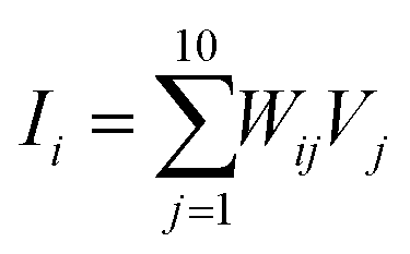 . The input signals are denoted by Vj with j = 1,…,9. V10 is a constant bias for accelerating the convergence process and the function's nonlinearity is controlled by β, finally, the adjustable (trainable) synaptic weights are labeled as Wij. This type of network is capable of classifying 3 × 3-pixel black and white images into three classes, with nine inputs corresponding to the pixel values. Three stylized letters ‘z’, ‘v’ and ‘n’ were tested on this network with 30 patterns (three sets) displayed in Fig. 6c. For example, there are a set of 10 versions of letter z and the first one in this set is the correct one. The rest 9 versions are the noisy (incorrect) ones, formed by flipping one of the pixels of the correct image. These sets were used for both training and testing due to the small set size. The bias input V10 was set to −0.1 V. Each input signal, voltage Vj was equal to either +0.1 V (+VR) or −0.1 V (−VR), corresponding to the black or white pixel respectively. Every two memristors are considered as a differential pair, a total of 60 memristors in the crossbar (30 × 2 = 60) were drawn in Fig. 6e. Fig. 6f elaborates an operation for pattern z. The input voltages can be determined by previously described rules and were applied to cross bar, and the resulting currents for each column (each top electrode bar) were evaluated then convert to perceptron's outputs with an activation function. These outputs were compared with the preset label values for letter z, n, v to get the differences which are known as the loss functions. Based on the loss function, back-calculate the adjustments of each weight using the gradient descent algorithm. This process is known as the back-propagation process. Fig. 6g presents the next step: the adjustments were physically established by using set pulse and reset pulse to tune the conductance of the synapses. When the output signal for the correct class of the applied pattern was higher than the signals for all other classes, the perfect classification was reached, on average, after 23 training epochs. It should be noted that the training of the network was performed in situ, without using an external computer model. Although this is a simple neural network only with one layer, it is a classical case study for examining if one possesses enough prerequisite knowledge about the algorithm to conduct advanced image processing characterizations. More importantly, it can be inferred that good reliability at single device level is required because realizing neural network on a memristive crossbar basically involves manipulations of numerous memristors with multiple conductance levels. Hence, the fundamental study on memristor at single device level remains of paramount importance. If researchers do not have access to crossbar fabrication, or prefer to work on optimizing performance at single device level, one can simulate the image processing performance like recognizing handwriting numbers for a single device level of memristor study by using an in-house software or simulator such as CrossSim.39,128–133
 | ||
| Fig. 6 Image processing fundamentals with memristor-based neuromorphic computing. (a) A simple neural network diagram. (b) A demonstration of the neural network on a memristive crossbar. Note, different shades of orange indicate different conductance at each junction. Reproduced with permission from ref. 126. Copyright 2019, Springer Nature, and image classification with metal-oxide memristors: (c) 3 × 3 binary image sets. (d) The schematic of single-layer perceptron for image classification. (e) Circuit demonstration of a 10 × 6 fragment of a memristive crossbar for this single-layer perceptron. (f) An illustration of the classification process for a specific input pattern (in this case, a stylized letter ‘z’), using input signals of +VR or −VR on the Al2O3/TiO2−x memristive crossbar, depending on the color of the pixel. (g) An illustration of the process of adjusting the weights in a specific column (in this case, the first positive column) based on a specific error matrix by using set/reset pulse VW± = ±1.3 V. Reproduced with permission from ref. 127. Copyright 2015, Springer Nature. | ||
8. Cyclic voltammetry (CV) and electrochemical impedance spectroscopy (EIS)
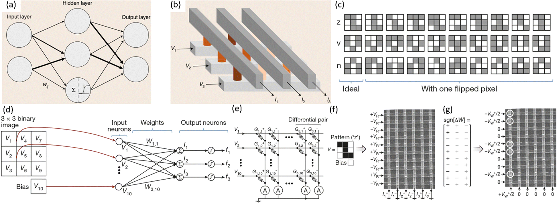
Cyclic voltammetry (CV) and Electrochemical Impedance Spectroscopy (EIS) are widely used to characterize electrochemical behaviors in various fields such as corrosion, electrocatalysis and battery.134–139 CV and EIS have also been employed to characterize the electrochemical behavior of memristors and hence enhance an understanding of the memristor behavior.140–144In memristor investigations, CV measurements can give insight into the redox processes happening before the switch events.145 Lübben et al. examined the electrochemical redox characteristics of various metals as active electrode materials within a M/SiO2/Pt system (M represents metal) spanning from noble to transition metals.145Fig. 7a summarizes the CVs of metal electrodes, demonstrating no significant passivation effects, i.e., no interfacial oxide was formed, indicating a reversible process. The general pattern is that the lower the nobility of a metal, the greater the negative potential required for reduction processes, with V, Ni, Fe, Cu, Ag, and Au ordered from most negative to most positive cell potential, with Au having the highest positive potential. The reaction rate varies among the active metals, with Cu, V, Au, and Ni having higher reaction rates, and Fe and Ag being less electrochemically active. Determining a clear order for oxidation reactions is difficult as most metals don’t exhibit a prominent oxidation peak. Fig. 7b compares the cyclic voltammograms of active electrode metals with high oxygen affinity. The first cycles are analyzed as they determine the formation of a passive film that impacts the shape and intensity of the CV curves. The potentials and currents of the peaks give insight into the redox reactions’ thermodynamic driving force and reaction rate. For instance, aluminum rapidly begins oxidation, but its dense barrier-type layer significantly reduces current and further oxidation. A 2–3 nm interfacial Al2O3 film is enough to passivate the device. In contrast, tantalum shows slower reaction rate, but can be oxidized over a wider voltage range to form oxide films up to several tens of nanometers, still permitting ionic motion. Titanium and Zirconium exhibit oxidation behavior between aluminum and tantalum, with Zr showing lower current densities and faster passivation compared to titanium. It's crucial to note that the crystallographic and defect-chemical structure of the interfaces formed also influences the device properties, not just the oxidation potentials. The choice of the counter electrode is equally important as the active electrode due to the electrochemical nature of filament formation.146,147 The starting point of filament formation is the counter electrode (typically BE), which is negatively biased during the SET process. The counter electrode's ability to catalyze reduction reactions is critical to the process.147 Cyclic voltammograms for various counter electrode materials of Cu/SiO2/CE (CE represent counter electrode) memristors are reported by Valov et al., of which the plots for noble metals are shown in Fig. 7c and Al in Fig. 7d.146,147 As shown, noble metal electrodes exhibit varying catalytic activity, with Ir being the most active followed by Ru, then Pt. From an electrochemical standpoint, devices using Ir or Ru electrodes should perform better, particularly in terms of switching time since their CV curves contained higher current density (j) peak than the Pt.147 Electrodes with a high affinity for oxygen, such as Al, are prone to passivation and inhibit further reactions. The results indicate that the counter electrode reaction rate is lower compared to that of the active electrode, which determines the reaction rate of the overall system. Increasing the counter electrode reaction rate leads to a higher reaction rate in the active electrode and, therefore, a shorter switching time. From the analysis above, we can see that CV measurements can be effective to provide foundational reference information for the selection of electrodes.
 | ||
| Fig. 7 Interpretation of CV and EIS characterizations with exemplary works. Comparison and categorization of the CV of the tested active electrode materials in SiO2-based memristors which can be classified based on their redox behavior: (a) reversible process, meaning that no passive film is formed, and the species can return to its original state. (b) Irreversible oxidation, where the formed product cannot be restored to its initial chemical state. Reproduced with permission from ref. 145. Copyright 2019, John Wiley and Sons, Influence of the CE material on the redox reactions preceding resistive switching: (c) CV plots of Cu/SiO2/CE memristors with various inert CE materials (Pt, Ir, and Ru). (d) Al, a passive metal that may form an interfacial oxide, as CE. Reproduced with permission from ref. 146. Copyright 2014, John Wiley and Sons, and EIS measurements on different states of Au/TiO2−x/TiO2/Au memristor: (e) EIS characteristics of the pristine device. Inset 1 displays a high-frequency spectrum. Inset 2 is the equivalent circuit. (f) After the SET process, A single contour was observed, revealing the device retained at LRS. The associated equivalent circuit is displayed in inset 1. Inset 2 is a schematic for LRS. (g) After the reverse voltage passed zero, two semicircles appeared, indicating the initiation of rupturing of filaments. The insets again demonstrate the equivalent circuit and schematic for the testing state. Reproduced with permission from ref. 150. Copyright 2018, Elsevier. | ||
The purpose of EIS is to analyze electrochemical systems and gain insight into the underlying electrochemical processes by measuring impedance changes at different sinusoidal frequencies.148 Accurate modeling is crucial to interpret the data, which is often accomplished through the use of equivalent circuit models.148 This non-invasive evaluation technique transforms EIS data into meaningful parameters such as capacitance (C), resistance (R), and constant phase element (CPE) that describe the electrochemical process.148 Nyquist plots, generated through EIS, effectively display the relationship between impedance and frequency.149 By using EIS to analyze memristor devices, which change their resistance in response to an applied electric field in a range of frequencies, we can gain insight into the different resistive regimes related to their switching behavior (SET/RESET). This nondestructive approach allows us to provide additional or supplementary evidence of the results obtained using TEM investigations which often require exquisite manipulations of the samples and specific accessories for memristive behaviors imaging.150 The impedance response of pristine Au/TiO2−x/TiO2/Au memristor cells was measured by Dash et al. at equilibrium (zero applied bias) to examine Z′′ vs. Z, where Z′′ is the imaginary part and Z′ is the real part of the impedance, at frequencies ranging from 1 MHz to 10 mHz.150 The results in Fig. 7e show two distinct resistive regimes in the Nyquist plot, confirmed by two semicircular frequency dispersion contours, likely attributed to the bilayer of TiO2−x and TiO2. The frequency dispersion was well within the bulk impedance response of resistive/capacitive. The resistance values of 57 kΩ and 65 kΩ for contour 1 and 2 respectively, indicate the relative resistances of non-stoichiometric TiO2−x and stoichiometric TiO2. To gain a deeper understanding of the impedance response at different switching states, impedance measurements were conducted as an ex situ analysis by interrupting the potential sweep at points where resistive changes occur. The resulting data showed a single impedance contour, which suggests the presence of a single charge transfer resistance (Rct) and interfacial capacitance connected in parallel, indicating that the formation of a filamentary galvanic contact with the TE had occurred. As depicted in inset 1 of Fig. 7f, this is supported by the equivalent circuit model. The researchers then applied a reverse voltage towards zero, and upon passing zero, they performed another EIS measurement. The spectrum returned to its original pristine-like state, with two clearly distinguishable impedance contours as shown in Fig. 7g.
Part II. Reliability issues in memristors
9. Endurance
Endurance is a key metric in evaluating a memristor's reliability, defined as the maximum number of cycles before failure occurs.151 However, most of the memristors suffer endurance degradation and/or failure after a number of switching cycles. The endurance is usually visualized by resistance/conductance versus cycle number graph. Chen et al. observed and categorized endurance failure symptoms into three types for their transition metal oxide (TMO)-based memristors with TiN and Pt electrodes: in Type I, RHRS decreasing and RLRS increasing occur simultaneously; in Type II, RLRS remains stable and RHRS decreases and RHRS suddenly drops to RLRS's level; and in Type III, RLRS keeps stable and RHRS gradually decreases to RLRS's level.152 Fadeeva and Rudenko also point out another two types of endurance failure/degradation symptoms which are basically opposite behaviors of Type II and Type III, meaning that RHRS is stable but RLRS increases gradually (Type V) or more abruptly (Type IV).153 These five types of failure and degradation behaviors are illustrated in Fig. 8(a–e) with trend lines. Fig. 8(f–j) present the practical examples of the associated categories.154 Physical mechanisms were suggested to understand these failure/degradation behaviors and these mechanisms are schematically explained in Fig. 8(k–n). Due to the nature of the TMO switching layer and noble electrodes, oxygen-related mechanisms govern the failures of Type I, II, and III.152 Type I is caused by a metal oxide barrier formed by Joule heating and oxygen ions creation during the forming processing, which blocks the transportation of electrons and oxygen ions.152 Type II can be explained as excess oxygen vacancies induced by an electrical field, which thickens the conductive filaments.152 Type III is attributable to the overabundant depletion of oxygen ions, caused by RESET processes, thus, reducing the likelihood of recombination between oxygen ions and oxygen vacancies and hence rupture of the conduction filament.152 The Type IV degradation of LRS is accounted by Zhao et al. for the presence of unrepairable and large gaps caused by the exhaustion of oxygen vacancies (Fig. 8n).151 They also describe an endurance evolution with the different voltage programming conditions, causing different failure/degradation types (Fig. 8o). Type II and III are also classified as stuck-at-LRS while Type IV and V as stuck-at-HRS, and Type I as stuck-at-MRS (MRS represents medium resistance state). Among them, stuck-at-LRS is the most common failure type, relating the unruptured conduction filament.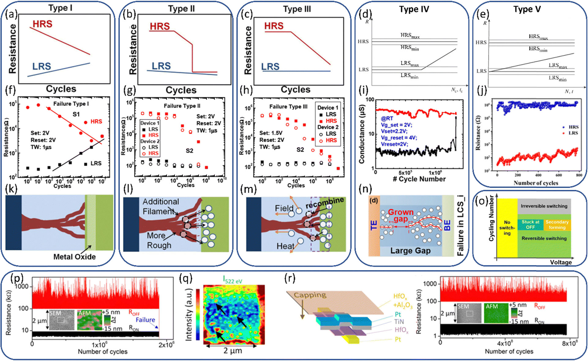 | ||
| Fig. 8 The failure modes associated with actual memristor failures, mechanisms and improvements in cycling endurance. Type I: (a) failure mode demonstration. Both RHRS and RLRS degrade and meet in the middle. (f) Measured data from TiN/HfOx/Pt memristor, with +2 V SET and −2 V RESET pulses, pulse time width (TW) is 1 μs. Note, RESET 2 V in the figure only represents its magnitude. This is also true for (g and h). (k) Illustration of failure mechanism. Type II: (b) trend lines for a sudden RRHS degradation mode. (g) Measured data from TiN/HfOx/TiOx/HfOx/TiOx/Pt memristor. The testing condition is the same as (f). (l) Schematic of failure mechanism. Solid line circles represent oxygen ions and dashed lines are oxygen vacancies. Type III: (c) graph of the gradual RRHS degradation mode. (h) Measured data from TiN/HfOx/Pt memristor, with +1.5 V SET and −2 V RESET pulses, pulse TW is 1 μs. (m) Corresponding mechanism explanation. The squared area with a dashed line is the interface between the switching layer and the electrode. Reproduced with permission from ref. 152. Copyright 2011, IEEE. Type IV: (d) failure mode illustration of steep RLRS degradation. (i) Measured data from HfO2/Al2O3 multilayer memristor with a transistor (1T1R). (n) Associated failure mechanism elaboration. White circles represent oxygen vacancies. And red lines symbolize conduction paths. (d) Reproduced with permission from ref. 153. Copyright 2021, published by Springer Nature. This is an open access article distributed under the terms of the Creative Commons CC BY license; (i and n) Reproduced with permission from ref. 151. Copyright 2019, published by IEEE. This is an open access article distributed under the terms of the Creative Commons CC BY license; Type V: (e) presentation of failure mechanisms of gradual HLRS degradation. (j) Measured data from K-birnessite MnO2-based memristor. (e) Reproduced with permission from ref. 153. Copyright 2021, published by Springer Nature. This is an open access article distributed under the terms of the Creative Commons CC BY license. (j) Reproduced with permission from ref. 154. Copyright 2020, American Chemical Society; (o) diagram of endurance versus operation voltage conditions describing the device states in (i). Reproduced with permission from ref. 151. Copyright 2019, published by IEEE. This is an open access article distributed under the terms of the Creative Commons CC BY license; and an example of endurance improvement: (p) Endurance characteristics of the reference device, a HfOx-based memristor. After about 2 × 10⁶ times cycling, the device encounters a stuck-at-LRS failure. The insets are associated SEM and AFM images obtained from failed devices, indicating severe damage to the top electrode. (q) Is the corresponding image by using scanning transmission X-ray microscopy, from which intensive morphology disorder was identified. (r) On the left, it is a schematic of redesigned HfOx-based memristor, and with the new structure, the cycling number increased up to ∼109, shown on the right. Reproduced with permission from ref. 164. Copyright 2017, AIP Publishing. | ||
The strategies for improving cycling endurance are desirable and enhanced endurance has been accomplished.155–162 For example, Kumar et al. demonstrated an improvement in endurance of about three orders of magnitude by modifying the device structure.163 The initial memristor structure consisted of Pt/TiN/HfO/Pt. With voltage pulse, the device ultimately malfunctioned by becoming permanently stuck in the ON state (stuck-at-LRS) after approximately 2 million cycles and was unable to be restored even when higher levels of DC bias were applied (Fig. 8p). Fig. 8q is the image of the failed device obtained through scanning transmission X-ray microscopy, where substantial fluctuations in intensity were observed, indicating widespread morphological disorder. Further X-ray and AFM analyses identified electrode damage as well as the separation and movement of oxygen. The failure in switching was likely due to one or more clusters that were highly lacking in oxygen becoming highly conductive and causing the electrodes to short permanently. To create a more consistent reservoir for excess oxygen and to prevent the formation of clusters, they increased the thickness of the TiN electrode layer. In addition, to accommodate high voltage or power spikes with a minimal temperature increase during memristor cycles, the thickness of the Pt electrodes was increased as well. Then, to make the top electrode more stable in terms of delamination or deformation, a capping layer of HfOx + Al2O3 was applied to cover the top electrode and the entire device. With the new device structure (Fig. 8r), the memristor exhibited repeated switching up to 109 cycles (Fig. 8r). Fujii et al. evaluated and compared cycling endurance for the SiO2 based memristors with various dimensions of the switching layer (i.e., SiO2).164 They found that cycling endurance was improved with scaling down the memristor's dimension. The device with a 30 nm size showed a cycling endurance of 104 cycles, while the one with 100 nm size experienced a much earlier failure after about 102 cycles. All devices ultimately experienced a RESET failure, i.e., stuck-at-LRS, suggesting the strong conductive filament was eventually formed and could not be ruptured, leading to a failure. Another failure was reported for SiO2-based memristors with Cu ions excessively doped into the switching layer, of which the stuck-at-LRS failure was also mitigated by scaling down the device. A spatial limitation in a smaller device may suppress the excessive injection and accumulation of Cu ions.
10. Variation
Memristors typically exhibit undesirable variations in resistance values and SET and RESET voltages from one device to device (also called D2D or spatial variation) and from one cycle to cycle (also called C2C or temporal variation).165,166 From the perspective of physical mechanism, the cycle-to-cycle variation originates from the stochastic formation and rupture of conductive filaments.43 The device-to-device variation stems from the limitations of fabrication techniques, which produce nonideal film morphology and homogeneity, resulting in the different electrical characteristics between memristors.167 It has been shown that by initializing plasma treatment, varying metallization, or inserting another layer, the temporal variation in I–V performance can be reduced.168–171Zhang et al. reported an improvement on the variation of IGZO-based memristor by nitrogen plasma treatment.169 For the reference Pt/IGZO/TiN memristor (untreated control sample), the I–V curves in Fig. 9a indicate that the switching parameters are not consistent, showing significant SET/RESET voltage variations over 100 cycles of DC sweeping. As a strategy to mitigate the variation, plasma treatment, generated from a mixed gas of N2:Ar (ratio of 50:12), was applied to modify the switching layer of IGZO. Before the plasma treatment, the sample was kept in the sputter chamber to limit exposure to air and undesirable any surface contaminations. As a result, an IGZO:N film was obtained after a plasma treatment time of 30 seconds. Subsequently, an additional 18 nm IGZO layer was deposited through sputtering. Fig. 9b shows the I–V characteristics for the Pt/IGZO/IGZO:N/TiN memristor, from which less variation on switching behaviors can be observed in Fig. 9b. And the distribution of the set voltages is statistically analyzed in Fig. 9c. It was observed that the IGZO:N device exhibits a narrower distribution of Vset in the range of 0.65 V to 0.75 V. In contrast, the distribution of Vset is much larger, 0.3–1.3 V in the untreated IGZO memristor. A model was established to clarify the contribution of the IGZO:N inserting layer on the enhanced variation. The model in Fig. 9d depicts the formation of oxygen vacancies that connect the Pt and TiN electrodes in the forming process. During operation, the connection and breaking of this oxygen-vacancy filament cause oxidation and reduction reactions (i.e., redox process) near the TiN electrode. In the Pt/IGZO/TiN device, the oxygen vacancies are recovered randomly, leading to widely distributed Vset and poor uniformity, particularly in HRS, as shown in Fig. 9d (left). The SET process of the Pt/IGZO/IGZO:N/TiN device is described schematically in Fig. 9d (right). The higher N–O bonding energy of 201 kJ mol−1 compared to the O–O bonding energy of 146 kJ mol−1 allows nitrogen atoms to easily capture and concentrate oxygen ions around the CF tips.172 This makes the IGZO:N layer act as an oxygen reservoir,169 enabling easier recombination between oxygen and oxygen vacancy and hence rupture of the conduction filaments (CFs), compared to the untreated Pt/IGZO/TiN device. The N atoms also help suppress the random formation of CFs, allowing the CF tips to grow along fixed paths in the IGZO:N layer, thereby improving the uniformity of set voltage distribution (i.e., less variation).
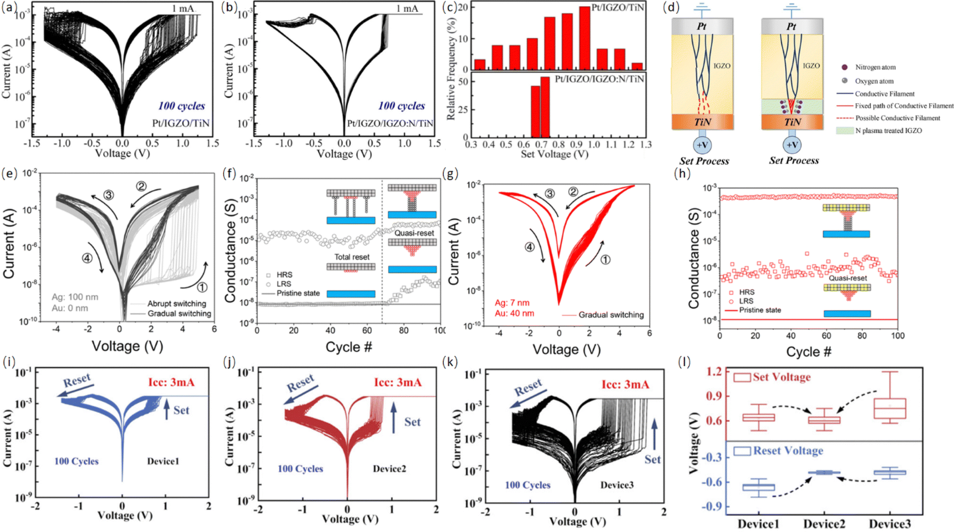 | ||
| Fig. 9 Non-ideal variation in the memristor performance and enhancement strategies. IGZO-based memristors: I–V characteristics in the semi-log scale of (a) reference Pt/IGZO/TiN memristor and (b) plasma treated Pt/IGZO:N/TiN. (c) Associated SET voltages distribution for both memristors for a comparison. (d) Schematical illustration for switching mechanisms of both memristors and the effect of plasma treatment on performance variation. Reproduced with permission from ref. 169. Copyright 2020, Elsevier, native SiOx based memristors: (e) I–V performance in the semi-log scale of a pure Ag/native SiOx/p++-Si, (f) corresponding endurance characteristics with schematics of total RESET and Quasi-RESET. (g) I–V cycling of native SiOx-based with Ag–Au composite TE and p++-Si BE. (h) Associated endurance with a schematic of the Quasi-RESET process. Reproduced with permission from ref. 171. Copyright 2022, American Chemical Society, and TaOx-based memristors: I–V characteristics in the semi-log scale of (i) reference Ta/TaOx/Pt memristor (Device1), (j) TaOx-based memristor with a 2 nm Al2O3 inserting layer, that is Ta/TaOx/2 nm Al2O3/Pt (Device2), and (k) Ta/TaOx/4 nm Al2O3/Pt (Device3). (l) Corresponding distribution of SET and RESET voltages for all three memristors. The statistical distribution of the SET and RESET voltages is narrow for the memristor with the 2 nm Al2O3 inserting layer. Reproduced with permission from ref. 177. Copyright 2023, published by John Wiley and Sons. This is an open access article distributed under the terms of the Creative Commons CC BY license. | ||
Ma et al. reduced performance variation for a native SiOx-based memristor by employing Ag–Au composite as top electrode.171 In Fig. 9e and f, the memristor with single Ag as TE exhibits a sudden switching behavior with large variations in set voltages at the start of switching cycles (as shown in Fig. 9d with gray lines). This significant switching variation is mainly due to the formation of multiple delicate conductive filaments.173,174 After a few switching cycles, the abrupt switching behavior of the device becomes uniform analog switching, as shown with black lines in Fig. 9e. This coincides with an increase in the conductance of HRS, as seen in Fig. 9f, which is indicative of a quasi-reset mode that is stabilized by residual (i.e., incompletely ruptured) Ag. In their theoretical study, the presence of residual Ag is the main cause of variation improvement of resistive switching due to the depressed randomness of the conductive filament since residual Ag localizes the electric field.175,176 To reduce the performance variation, the top electrode was redesigned: an Ag–Au composite was deposited on the native SiOx layer, then the entire structure was capped with a pure Au layer. The I–V characteristics for the new design are displayed in Fig. 9g and h. Less variation is observed from the beginning of switching, i.e., there is no transition from abrupt to analog switching. The active Ag in the Ag–Au composite is not continuous anymore because it is isolated by Au. The injection of Ag cations from the Ag–Au composite electrode is not widespread anymore, thus fewer but stronger Ag conductive filaments were formed during the initial set, resulting in a quasi-reset. This is further validated by the enhancement in retention characteristics.
Jiang et al. reported less variation of TaOx-based memristor by inserting an Al2O3 layer between the switching layer and Pt bottom electrode.177 The reference Ta/TaOx/Pt memristor (Device1) was characterized by I–V sweeping and the result of 100 cycling is shown in Fig. 9i. Under the same testing condition, the characteristics of TaOx-based memristors by inserting a 2 nm- (Device2) and 4 nm-thick (Device3) Al2O3 layer are displayed in Fig. 9j and k, respectively. From these I–V semi-log representations, Device2 has a higher on/off ratio and less variation than Device1. Device3 also has a high on/off ratio but appears more variation than Device1 and Device2. The statistics distribution of the SET and RESET voltages of the three devices in Fig. 9l present the variation differences in a quantitative way, confirming Device2 with a 2 nm inserting layer has the best performance in terms of variation. The authors proposed the following mechanisms behind the phenomena. The Al2O3 layer can be considered a limiting layer for the diffusion of oxygen ions.177–180 Thus, the Al2O3 layer can be used to engineer the conductance modulation of the Ta/TaOx/Al2O3/Pt memristor, by which the switching mechanism is modified and the DC sweeping characteristics are expected to be enhanced. Compared to the control memristor (i.e., without the Al2O3 insertion layer), the oxygen ions along with the CFs are confined within the Al2O3 layer, leading to a quicker formation and disruption of the CFs.177 However, employing a thicker inserting layer increased the variation. This could be due to the increased limiting effect of oxygen ion diffusion caused by a higher concentration of Al ions in the Al2O3 layer, leading to a more randomized connection and disconnection of the conductive filaments.177 Therefore, optimization of the inserting layer's thickness is decisive as well.
11. Retention
Retention time is another technological merit to characterize the performance in terms of memristors’ reliability.177,181–188 The retention time is defined as, after the electrical bias is removed, the time duration that keeps each resistive state stable. Fig. 10a presents a comparison of retention time characteristics between an early failed reference sample-1 (Pt/HfOx/Ti memristor) and a long retention sample-3.189 The current level of sample-1 was read with 0.1 V every 5 seconds at 85 °C. After 100 s, the resistive states changed abruptly (i.e., resistance dropped), indicating the storage information in the memristor was lost. With modified bottom electrode Ti by polydopamine (PDA)/Ag nanoparticles (AgNPs), sample-3's HRS and LRS last 104 s under the same measurement conditions. The longer retention time of sample-3 was ascribed to the local electrical field enhancement of AgNPs. It is widely accepted that the memristor should have 10 years of retention time at 85 °C for practical applications, and such long-time testing is not realistic, so the data are extrapolated to get an estimation. In Fig. 10b, the data from retention test of a Cu/α-Si (amorphous Si)/α-C (amorphous C)/Pt device in a memristor crossbar array at 100 °C is displayed.190 The resistive states kept stable for more than 105 s and the data's extrapolation reached 10 years of retention time approximately. The mechanism of retention was related to the conductive filament's rupture. Im et al. enhanced the retention time of Halide perovskites (HPs) based memristors by modulating the Ag doping concentration and suggested related mechanisms.191 There is a persistent tendency for the conductive filament to diffuse out, and so its conductive network is broken down. This is caused by the chemical potential gradient at the filament's surface and the desire to minimize its surface energy.191–195 Based on the Gibbs–Thomson effect, the surface atomic flux (Js) on the filament surface determines the lifespan of conductive filament, and Js strongly depends on the filament's radius.191,195 The larger radius yields a slower surface diffusion. Fig. 10c shows that the retention time changes with the Ag concentrations in CH3NH3PbI3 (MAPbI3):Ag-based memristors. A transition from volatile threshold switching (temporary switching) to non-volatile resistive switching was observed. With a rise in the Ag doping concentration, there was a corresponding increase in retention time. The mechanisms of threshold, resistive switching, and transition were proposed in Fig. 10d. Low Ag concentration devices induce weak filaments with a smaller radius due to the limited Ag concentration. As discussed previously, a smaller radius of filaments leads to larger Js, i.e., faster surface diffusion.191,195 Thus, the removal of the external field annihilates the weak filaments, resulting in a shorter retention time. In a similar way, the higher Ag doping concentration prolonged lifetime of the filament by slowing down the diffusion. It is desirable to achieve multiple conductance states with long retention time, especially for neuromorphic computing, which may require additional components in the device structure (i.e., changing device structure). Wang et al. demonstrated a superlattice-like (SLL) structure memristor (Fig. 10e) by incorporating several layers of alternating AlOy (yellow) with the HfOx functioning layer.196 Under the test condition of 100 mV read voltage and 1 second read interval at 85 °C, Fig. 10f shows that eight conductance states remained stable for more than 104 s without considerable drift. Adding several AlOy barrier layers to the HfOx switching layer reduced the strength of the Vo conductive filament, by which the formation and rupture process becomes gradual. Then, multiple states were achieved because oxygen ions must continuously pass through the barrier layers when exposed to successive pulses of limited energy during the migration process. Besides the barriers, Hf–O–Al bond on oxygen atoms triggered the confinement effect, thus, the relaxation of the conductive filament was controllable. Another method for improving retention characteristics is to change the morphology of the switching layer. Hu et al. used unique vertical nanosheet CuInS2 (CIS) arrays featuring nanoscale pores rather than conventional CIS film as the functioning layer (Fig. 10g).197Fig. 10h is the top view high-magnification SEM image of the CIS nanosheets layer. The retention time for nanosheets CIS-based memristor was reported as much enhanced 104 s, compared to that of the conventional film-based memristor. The enhancement was attributed to the network-limited vertical structure and efficient isolation of leakage paths by the demonstrated porous structure.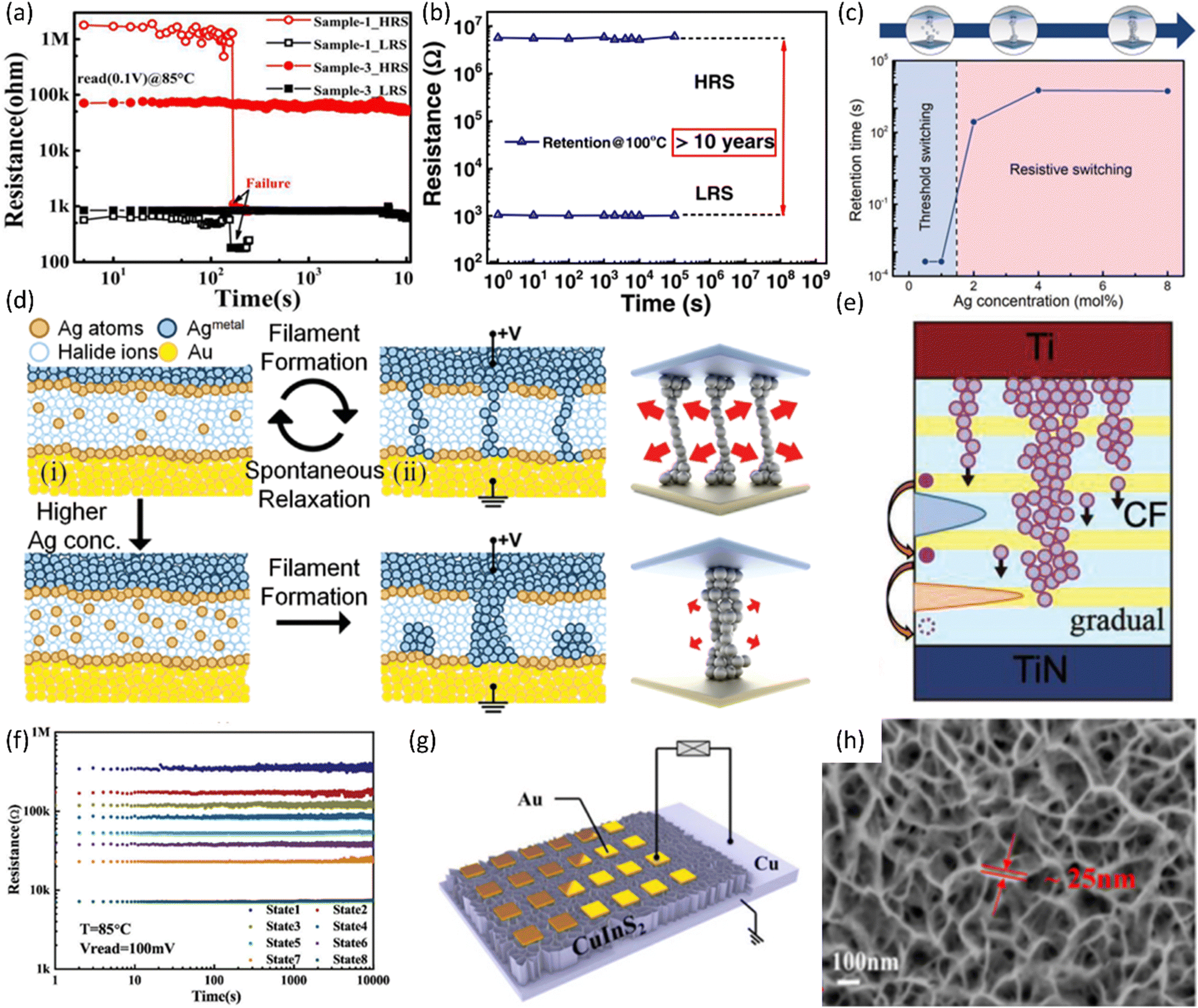 | ||
| Fig. 10 Representative retention behaviors of memristors. (a) Retention characteristics at 85 °C of sample-1 Pt/HfOx/Ti and sample-3 PDA/AgNPs modified TE memristors. Reproduced with permission from ref. 189. Copyright 2021, AIP Publishing, (b) retention measurement on Cu/α-Si/α-C/Pt memristor at 100 °C, and the extrapolated retention, reaching 10 years of retention. Reproduced with permission from ref. 190. Copyright 2022, published by John Wiley and Sons. This is an open access article distributed under the terms of the Creative Commons CC BY license, MAPbI3:Ag-based memristors: (c) the relationship between retention time and the Ag doping concentration. (d) The schematic of the mechanisms of the threshold and resistive switching. Reproduced with permission from ref. 191. Copyright 2022, John Wiley and Sons, Superlattice-like (SLL) structure memristors: (e) the design of Ti/(HfOx/AlOy)SLL/TiN memristor, where yellow colored layers are AlOy and layers with light blue represent HfOx. (f) At 85 °C, retention characteristics of eight conductance levels. Reproduced with permission from ref. 196. Copyright 2022, published by John Wiley and Sons. This is an open access article distributed under the terms of the Creative Commons CC BY license, and Nanosheets CIS-based memristor: (g) structure of memristive arrays with Au top electrodes. (h) Top view SEM image of the CIS nanosheets layer. Reproduced with permission from ref. 197. Copyright 2023, The Royal Society of Chemistry. | ||
12. Linearity
In the section on image processing, we reviewed a neural network implemented by a memristive crossbar for in situ backpropagation training. One of the key takeaways that we gleaned from that characterization method is that synaptic weight was denoted as memristor's conductance (G), and it was modulated continuously during the training. In a view of the single device level, this kind of modulation can be considered as that memristor mimics the long synaptic plasticity including long-term potentiation (LTP) and long-term depression (LTD). The LTP process increases the conductance of the memristor and LTD decreases it. These processes are induced by applying the opposite bias of the pulse train and visualized in Fig. 11a with an inset image of a memristive crossbar.198 It is preferable to tune the memristor in a linear and symmetric manner, ensuring that every electrical stimulus (e.g., pulse count or width) elicits an equal update of conductance during both potentiation (SET) and depression (RESET) transitions.199 However, in reality, the LTP and LTD processes are plagued by non-linearity and asymmetry issues from the conductance modulation. The symptoms of these issues were summarized in Fig. 11b. By applying identical pulses (i.e., same duration and the same amplitude, but opposite directions for the two train), the red line symbolizes the ideal correspondence between conductance and the number of pulses, and the black curve portrays the one for an actual memristor device. In a LTP process, for a scenario where the conductance of a memristor is required to be increased from a to b, the ideal linear function is usually used to calculate the needed pulse stimuli.198 Yet, upon application of the calculated pulses to the actual memristor, the conductance deviates from its expected trajectory and shifts from point a to c instead of from point a to b. A comparable error in weight updating happens during the LTD process. As a result, the actual updates in conductance and the desired change are vastly disparate due to the nonlinearity issue, which subsequently diminishes the accuracy of the neural network computing. One alternate mechanism behind the nonlinearity issue is the presence of two phases in the evolution process of the conductive filament.200 Using the creation of the filament as an illustration, the first stage involves the growth of the conductive filament until it connects the bottom and top electrode, which is regulated by the drift of metallic ions or oxygen vacanccies200–202 Once the filament is formed, it tends to further thicken by ion diffusions.200,202–204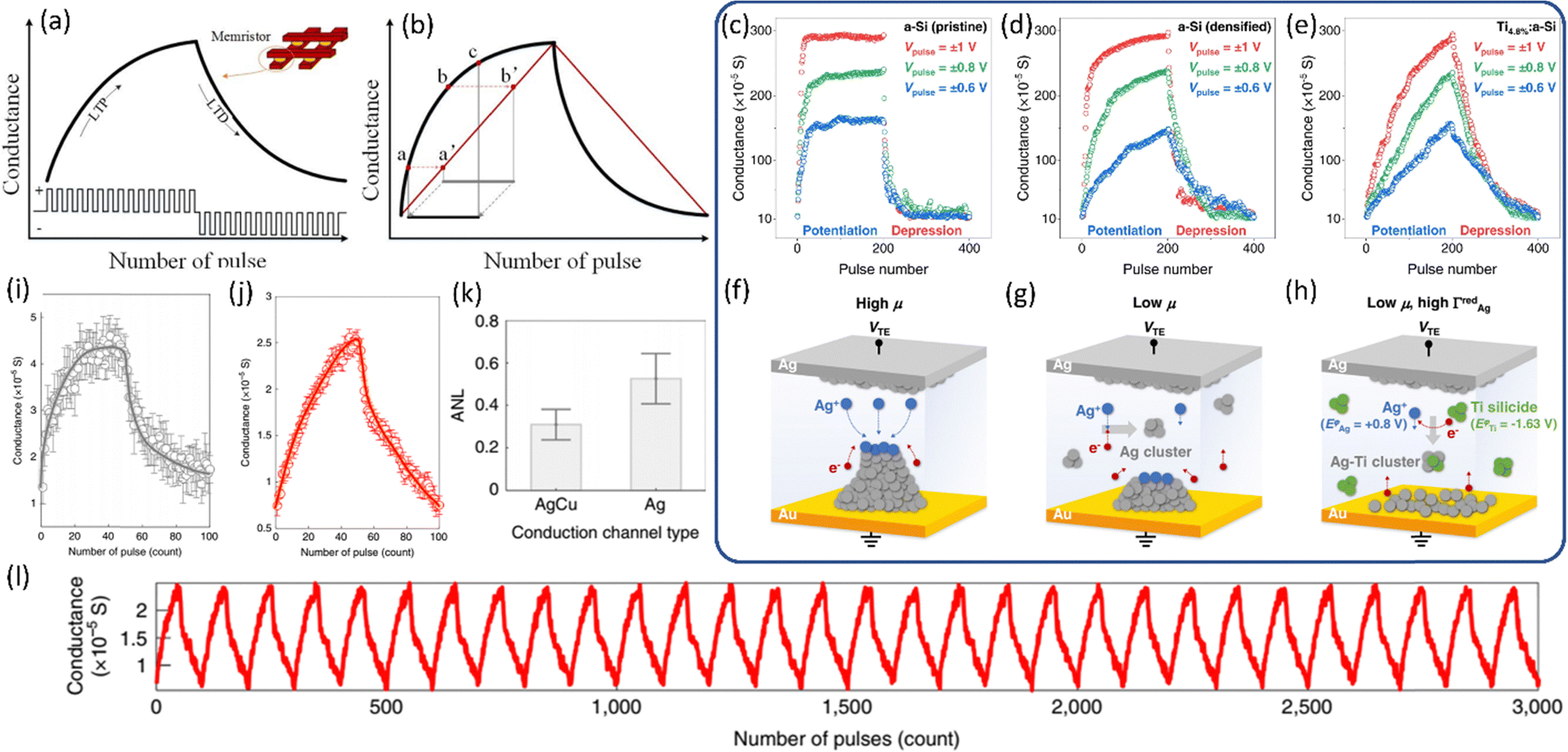 | ||
| Fig. 11 Demonstration of synaptic weight updating process: (a) conductance changes by applying identical pulses (b) weight updating process based on ideal linearity. Reproduced with permission from ref. 198. Copyright 2019, IEEE, synaptic weight updating performance and mechanisms on memristors with the switching layer of (c and f) low-density a-Si, (d and g) densified a-Si, and (e and h) Ti nanoclusters embedded densified a-Si. Reproduced with permission from ref. 209. Copyright 2022, Springer Nature, and conductance changes of Si-based memristor by applying nanosecond scale pulses with (i) Ag only top electrode and (j) Ag–Cu alloying one. (k) Associated statistics report on ANL of these two kinds of memristors. (l) 30-Cycle conductance programming of AgCu alloying memristor. Reproduced with permission from ref. 210. Copyright 2020, Springer Nature. | ||
The strategies such as material engineering have been employed to attain desirable linearity.205–208 Kang et al. achieved an improved linearity of amorphous Si (a-Si)-based memristors through densification of the switching layer a-Si.209 The linearity was further enhanced by the inclusion of Ti nanoclusters. Fig. 11c shows the a-Si-based memristor suffered a non-linearity issue, under three different amplitudes of pulses and a filamentary mechanism is illustrated in Fig. 11f. They claimed that the relatively low density of a-Si leads to high cation mobility, thus the injected Ag ions rapidly arrive at the bottom electrode and reduce and accumulate there. Consequently, the filament that grows from the bottom experiences strong reinforcement from the local electric field, resulting in a non-linear issue. So, a densified a-Si memristor was fabricated to slow the ions’ migration so that the Ag-clusters are formed inside the a-Si to reduce the buildup of silver (Fig. 11g). Its performance was plotted in Fig. 11d and the improvements on linearity were observed, especially with low amplitudes of pulses. The large dynamic range, i.e., on/off ratio, is important to memristors, thus, the linearity with high pulse amplitudes should continue to be optimized. They introduced Ti nanoclusters with negative reduction potential to capture and reduce the migrating Ag cations to Ag-clusters (Fig. 11h). The linearity results summarized in Fig. 11e manifest the enhancements with all three pulse amplitudes due to the increased reduction probability of Ag cations inside the a-Si switching layer. The quantitative evaluation method for linearity was clearly described in this work as well. Yeon et al. demonstrated that alloying top electrode helps alleviate the nonlinearity issue.210Fig. 11i is a linearity examination for a Si-based memristor with a commonly used Ag top electrode, and shows a sudden drop of conductance, indicating a nonlinearity issue. With the Ag–Cu alloying, a more linear and symmetric switching was achieved (Fig. 11j) and the asymmetric non-linearity factor (ANL) was calculated to characterize the improvement which drops to an average value from 0.59 to 0.3 with Ag only devices (Fig. 11k). They speculated the alloying yields a stabilized interaction of conduction channels to refine the performance of conductance updating. 30 cycles of LTP/LTD on Ag–Cu alloying memristor were measured by using nanosecond scale width for the pulses and associated results were displayed in Fig. 11l. Engineering pulsing scheme may also address the nonlinearity challenge;211,212 however, the linearity and symmetry problems need to be more fundamentally mitigated by engineering materials structures and properties, and the associated device architecture.200
Part III. Theoretical calculations
13. Density functional theory (DFT) and molecular dynamics (MD) simulations
Density functional theory (DFT) and molecular dynamics (MD) simulations are extensively leveraged to study the electronic structure of materials and the dynamic behavior of atoms and molecules, which is often difficult to be identified with macroscale characterizations, in the fields of physics, chemistry, and materials science.213–216 Regarding memristors, these simulation methods are commonly employed to investigate the switching mechanisms, assist in device design, and provide support for experimental findings.217–223Zhu et al. optimized the amorphous HfO2 (a-HfO2)-based memristor performance with an additional Al-doped HfO2 layer (i.e., bilayer structure).224 The Pt/HfO2:Al/HfO2/TiN memristor demonstrated enhanced cycling endurance and less cycle-to-cycle variation. DFT simulation was employed to study the properties of the HfO2:Al layer which provided a foundation to explain the switching mechanism and the underlying reasons for the enhancements. Fig. 12a displays the statistical distribution of the calculated formation energies of VO in a-HfO2 and a-HfO2:Al, which were calculated at ten different positions within the considered unit cell of the two cases, reflecting the disordered states of amorphous materials (i.e., HfO2). In a-HfO2, the average VO formation energy is approximately 6.24 eV, whereas in a-HfO2:Al, it is 3.29 eV, indicating that VO is more easily generated with the incorporation of Al. Fig. 12b and c illustrate the diffusion barrier profiles of VO migration in a-HfO2 and a-HfO2:Al, simulated by relocating the oxygen atom from its original site to neighboring vacancies. The migration barrier of VO in a-HfO2 is 2.72 eV, compared to 2.21 eV in a-HfO2:Al, indicating that VO can migrate more easily in a-HfO2:Al. Consequently, the VO CF is likely to have a greater preference for growth in a-HfO2:Al.
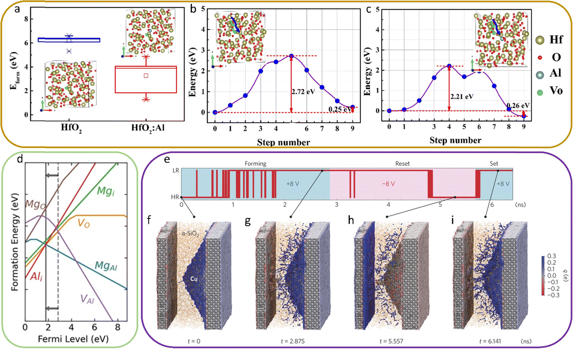 | ||
| Fig. 12 DFT and MD simulations for device design and mechanism exploration. DFT simulations for aHfO2-based memristors with Pt TE and TiN BE: (a) the formation energy distribution of oxygen vacancies in a-HfO2 and a-HfO2:Al. The insets display the a-HfO2 and a-HfO2:Al structures with a VO. Reproduced with permission from ref. 224. Copyright 2021, Elsevier, DFT simulations for Al2O3-based memristors with Pd TE and Al BE: (d) The defect formation energy of native and Mg-related defects in Al2O3 as a function of the Fermi level. Reproduced with permission from ref. 225. Copyright 2022, Springer Nature, MD simulations for SiO2-based memristors: (e) the scale indicates how the SiO2-based memristor switches on and off in response to the simulation time. The evolution of atomic structure and charge states is represented at (f) initial HRS, (g) forming LRS, (h) HRS, and (i) SET LRS. Reproduced with permission from ref. 226. Copyright 2015, Springer Nature. | ||
Goul et al. reported tunable on/off ratio Al2O3-based memristors guided by their DFT simulation results.225Fig. 12d displays the computed defect formation energy plotted against the Fermi level location. The graph showcases the results for native defects, such as VO, aluminum vacancy (VAl), and aluminum interstitial (Ali), and defects from Mg doping, including Mg substituting on Al (MgAl), Mg substituting on Al (MgO), and Mg interstitials (Mgi) under both Al-rich and O-rich conditions. By introducing Mg in the DFT calculation, the anticipated position of the Fermi level will relocate towards the valence band maximum, as indicated by the arrows and solid vertical lines in Fig. 12d. This downward Fermi level shift yields two benefits for improving the performance of Al2O3-based memristors: firstly, a reduced Fermi level implies greater insulation/resistance in the HRS of Mg-doped Al2O3. Secondly, at these lower Fermi levels, the formation energy of VO is decreased, indicating that a greater number of VO will form. Following the DFT calculations, interfacial MgO layer(s) as the method of Mg doping is implemented in the Al2O3 switching layer to engineer the switching performance of Al2O3-based memristors.
Onofrio et al. simulated ECM switching behaviors in a SiO2-based memristor by the MD method.226 The active electrode was Cu and its surface was designed with triangular or conical patterns to emulate the unevenness, typically observed in actual samples. Fig. 12e depicts the cell's resistance state over time as a result of the simulation, while Fig. 12f–i exhibit atomic snapshots capturing crucial stages of the process. Applying the initial forming voltage causes the Cu atoms near the active electrode's surface to become positively charged (blue atoms in Fig. 12f), which increases their likelihood of dissolving into the SiO2 electrolyte. Within one nanosecond, the simulations indicate that these dissolved atoms form the first bridging filaments. Interestingly, these early connections are short-lived, unstable states consisting of a single-atom chain, and the device switches back and forth between the on and off states for another nanosecond until a stable filament is formed. The snapshots in Fig. 12g display the stable nanofilament that bridges the electrodes, along with other partially grown filaments linked to the inactive electrode. With a negative bias, the filament fractures near the inactive electrode, leaving behind an incomplete filament that is now attached to the active electrode (refer to Fig. 12h). After the RESET, applying a positive bias quickly creates a new connection (shown in Fig. 12i), effectively turning the device back on. The MD simulations offer a detailed view of the operational mechanisms at an atomic level, and with a superior time resolution.
In summary of this section, DFT and MD simulations are effective methods for studying the formation energy of defects, the energy barriers of ion migration, and the dynamics of resistive switching at the atomic level, which will be valuable supplements to instrumental characterizations.
14. Conclusions and perspectives
This review comprehensively focuses on the two main aspects of memristors and their potential energy-efficient neuromorphic computing. As one of the focused topics of characterizations for memristor materials and devices, structure, chemical and electronic evaluation techniques such as TEM, XPS, and AFM are of crucial importance to examining the device structure, identifying the switching mechanisms, and engineering the switching layer (e.g., composition and dimension). Figures of merit performance of memristor devices are generally determined by various electrical measurements. DC sweeping provides a variety of fundamental characteristics, including bipolar switching behavior, on/off ratio, endurance, and conduction mechanism. Pulse measurements are another instrumental electrical characterization method to evaluate endurance behaviors in a way closer to practical application while linearity needs to be considered for neural network establishment. Advanced image processing is a characterization method to evaluate analog tuning accuracy. CV and EIS are widely used in electrochemical research, and they are also introduced for exploring the selection criterion of electrode materials and switching mechanisms of memristors. As another main subject, the reliability of memristors is typically evaluated by four criteria including endurance, variation, retention, and linearity. Each of these reliability issues is discussed in-depth and corresponding characteristics indicators, mechanisms, and measurement standards are provided and elaborated. Possible mitigation approaches to these reliability concerns are suggested as well. DFT and MD simulations play an important role in the design process, aiding in the interpretation of experimental results and facilitating an understanding of switching behaviors.The memristor has been theoretically proposed for more than forty years, and experimental efforts have been made actively for more than a decade. However, some of the fundamentals stay controversial, and the commercial adoption of memristors is still hindered due to the lack of these fundamentals and reliability issues. Further endeavors must be pursued to rectify these limitations. Besides applying memristors to numerous applications, it is urgent to objectively report the characteristics, clarify the key issues of various non-ideal performance and identify the underlying mechanisms. Researchers from diverse fields still possess a remarkable opportunity to drive the progression of memristors by further establishing the switching/failure mechanisms with both typical and novel characterization techniques. In addition, strategic designs of materials and devices can address multiple reliability concerns simultaneously. For instance, as demonstrated in Yeon et al.'s study reviewed in the linearity section, the Ag–Cu electrode alloying significantly improved both the variation and retention as well at the single device level, which in turn leads to reliable crossbar arrays.210 Also, as this example shows, the improvements in crossbar performance frequently stem from single-device level optimization, thus, the examination at the single-device level remains crucial and is still highly recommended in this field. Meanwhile, with booming neuromorphic applications, materials researchers should acquire knowledge of neural networks to address the issues at a single-device level and synergistically collaborate with data science and circuit engineers for practical computing applications. We believe that advancing the characterization methods will continue enhancing the memristor's fundamentals and understanding the reliability issues constitutes a vital step towards optimizing the functioning of the memristor.
Conflicts of interest
There are no conflicts to declare.Acknowledgements
This work was supported by the U.S. National Science Foundation (NSF) Awards ECCS-1931088 and CBET-2207302. S. L. and H. W. S. acknowledge the support from the Improvement of Measurement Standards and Technology for Mechanical Metrology (Grant No. 23011043) by KRISS. The authors would like to thank Xingyu Fu and Fengfeng Zhou for the constructive discussion on Image processing.References
- L. Chua, IEEE Trans. Circuit Theory, 1971, 18, 507–519 Search PubMed
.
- J. J. Yang, M. D. Pickett, X. Li, D. A. A. Ohlberg, D. R. Stewart and R. S. Williams, Nat. Nanotechnol., 2008, 3, 429–433 CrossRef CAS PubMed
- D. B. Strukov, G. S. Snider, D. R. Stewart and R. S. Williams, Nature, 2008, 453, 80–83 CrossRef CAS PubMed
- D. B. Strukov, G. S. Snider, D. R. Stewart and R. S. Williams, Nature, 2009, 459, 1154 CrossRef CAS
- N. D. Mathur, Nature, 2008, 455, E13 CrossRef CAS
- J. J. Yang, M. X. Zhang, J. P. Strachan, F. Miao, M. D. Pickett, R. D. Kelley, G. Medeiros-Ribeiro and R. S. Williams, Appl. Phys. Lett., 2010, 97, 3–5 Search PubMed
- X. Li, H. Wu, G. Bin, W. Wu, D. Wu, N. Deng, J. Cai and H. Qian, Nanotechnology, 2016, 27, 305201 CrossRef PubMed
- Y.-E. Syu, T.-C. Chang, J.-H. Lou, T.-M. Tsai, K.-C. Chang, M.-J. Tsai, Y.-L. Wang, M. Liu and S. M. Sze, Appl. Phys. Lett., 2013, 102, 172903 CrossRef
- Z. Fang, H. Y. Yu, W. J. Liu, Z. R. Wang, X. A. Tran, B. Gao and J. F. Kang, IEEE Electron Device Lett., 2010, 31, 476–478 CAS
- S. U. Sharath, S. Vogel, L. Molina-Luna, E. Hildebrandt, C. Wenger, J. Kurian, M. Duerrschnabel, T. Niermann, G. Niu, P. Calka, M. Lehmann, H.-J. Kleebe, T. Schroeder and L. Alff, Adv. Funct. Mater., 2017, 27, 1700432 CrossRef
- C. H. Kim, Y. H. Jang, H. J. Hwang, C. H. Song, Y. S. Yang and J. H. Cho, Appl. Phys. Lett., 2010, 97, 1–3 Search PubMed
- M. C. Chen, T. C. Chang, S. Y. Huang, S. C. Chen, C. W. Hu, C. T. Tsai and S. M. Sze, Electrochem. Solid-State Lett., 2010, 13, 191–194 CrossRef
- Z. Q. Wang, H. Y. Xu, X. H. Li, X. T. Zhang, Y. X. Liu and Y. C. Liu, IEEE Electron Device Lett., 2011, 32, 1442–1444 CAS
- Z. Q. Wang, H. Y. Xu, X. H. Li, H. Yu, Y. C. Liu and X. J. Zhu, Adv. Funct. Mater., 2012, 22, 2759–2765 CrossRef CAS
- M. S. Kim, Y. Hwan Hwang, S. Kim, Z. Guo, D. I. Moon, J. M. Choi, M. L. Seol, B. S. Bae and Y. K. Choi, Appl. Phys. Lett., 2012, 101, 3–6 Search PubMed
- Y. S. Fan, P. T. Liu and C. H. Hsu, Thin Solid Films, 2013, 549, 54–58 CrossRef CAS
- Y. H. Hwang, H. M. An and W. J. Cho, Jpn. J. Appl. Phys., 2014, 53, 1–4 Search PubMed
- Y. Pei, B. Mai, X. Zhang, R. Hu, Y. Li, Z. Chen, B. Fan, J. Liang and G. Wang, J. Electron. Mater., 2015, 44, 645–650 CrossRef CAS
- C. C. Lo and T. E. Hsieh, J. Phys. D: Appl. Phys., 2016, 49, 385102 CrossRef
- Q. Li, Y. Li, L. Gao, F. Ma, Z. Song and K. Xu, RSC Adv., 2016, 6, 42347–42352 RSC
- F. Qin, Y. Zhang, H. Park, C. S. Kim, D. H. Lee, Z.-T. Jiang, J. Park, K. No, H. Park, H. W. Song and S. Lee, Phys. Status Solidi RRL, 2022, 16, 2200075 CrossRef CAS
- M. A. Zidan, H. A. H. Fahmy, M. M. Hussain and K. N. Salama, Microelectron. J., 2013, 44, 176–183 CrossRef
- T. You, N. Du, S. Slesazeck, T. Mikolajick, G. Li, D. Bürger, I. Skorupa, H. Stöcker, B. Abendroth, A. Beyer, K. Volz, O. G. Schmidt and H. Schmidt, ACS Appl. Mater. Interfaces, 2014, 6, 19758–19765 CrossRef CAS PubMed
- H. Jeong and L. Shi, J. Phys. D: Appl. Phys., 2019, 52, 023003 CrossRef
- W. Q. Pan, J. Chen, R. Kuang, Y. Li, Y. H. He, G. R. Feng, N. Duan, T. C. Chang and X. S. Miao, IEEE Trans. Electron Devices, 2020, 67, 895–901 CAS
- K. Sun, J. Chen and X. Yan, Adv. Funct. Mater., 2021, 31, 1–33 Search PubMed
- H. Kim, M. P. Sah, C. Yang, T. Roska and L. O. Chua, Proc. IEEE, 2012, 100, 2061–2070 Search PubMed
- S. H. Jo, T. Chang, I. Ebong, B. B. Bhadviya, P. Mazumder and W. Lu, Nano Lett., 2010, 10, 1297–1301 CrossRef CAS PubMed
- D. V. Christensen, R. Dittmann, B. Linares-Barranco, A. Sebastian, M. Le Gallo, A. Redaelli, S. Slesazeck, T. Mikolajick, S. Spiga, S. Menzel, I. Valov, G. Milano, C. Ricciardi, S.-J. Liang, F. Miao, M. Lanza, T. J. Quill, S. T. Keene, A. Salleo, J. Grollier, D. Marković, A. Mizrahi, P. Yao, J. J. Yang, G. Indiveri, J. P. Strachan, S. Datta, E. Vianello, A. Valentian, J. Feldmann, X. Li, W. H. P. Pernice, H. Bhaskaran, S. Furber, E. Neftci, F. Scherr, W. Maass, S. Ramaswamy, J. Tapson, P. Panda, Y. Kim, G. Tanaka, S. Thorpe, C. Bartolozzi, T. A. Cleland, C. Posch, S. Liu, G. Panuccio, M. Mahmud, A. N. Mazumder, M. Hosseini, T. Mohsenin, E. Donati, S. Tolu, R. Galeazzi, M. E. Christensen, S. Holm, D. Ielmini and N. Pryds, Neuromorphic Comput. Eng., 2022, 2, 022501 CrossRef
- C. Sung, H. Hwang and I. K. Yoo, J. Appl. Phys., 2018, 124, 151903 CrossRef
- H. Jiang, D. Belkin, S. E. Savel’Ev, S. Lin, Z. Wang, Y. Li, S. Joshi, R. Midya, C. Li, M. Rao, M. Barnell, Q. Wu, J. J. Yang and Q. Xia, Nat. Commun., 2017, 8, 882 CrossRef PubMed
- Q. Liu, J. Sun, H. Lv, S. Long, K. Yin, N. Wan, Y. Li, L. Sun and M. Liu, Adv. Mater., 2012, 24, 1844–1849 CrossRef CAS PubMed
- J. Y. Chen, C. W. Huang, C. H. Chiu, Y. T. Huang and W. W. Wu, Adv. Mater., 2015, 27, 5028–5033 CrossRef CAS PubMed
- F. Yuan, Z. Zhang, C. Liu, F. Zhou, H. M. Yau, W. Lu, X. Qiu, H. S. P. Wong, J. Dai and Y. Chai, ACS Nano, 2017, 11, 4097–4104 CrossRef CAS PubMed
- Z. Wang, S. Joshi, S. E. Savel’ev, H. Jiang, R. Midya, P. Lin, M. Hu, N. Ge, J. P. Strachan, Z. Li, Q. Wu, M. Barnell, G.-L. Li, H. L. Xin, R. S. Williams, Q. Xia and J. J. Yang, Nat. Mater., 2017, 16, 101–108 CrossRef CAS PubMed
- J. Yin, F. Zeng, Q. Wan, F. Li, Y. Sun, Y. Hu, J. Liu, G. Li and F. Pan, Adv. Funct. Mater., 2018, 28, 1706927 CrossRef
- X. Yan, J. Zhao, S. Liu, Z. Zhou, Q. Liu, J. Chen and X. Y. Liu, Adv. Funct. Mater., 2018, 28, 1705320 CrossRef
- I. Zrinski, C. C. Mardare, L.-I. Jinga, J. P. Kollender, G. Socol, A. Minenkov, A. W. Hassel and A. I. Mardare, Nanomaterials, 2021, 11, 666 CrossRef CAS PubMed
- Y. R. Park, H. Cho and G. Wang, ACS Appl. Electron. Mater., 2022, 4, 3739–3748 CrossRef CAS
- S.-J. Choi, G.-S. Park, K.-H. Kim, S. Cho, W.-Y. Yang, X.-S. Li, J.-H. Moon, K.-J. Lee and K. Kim, Adv. Mater., 2011, 23, 3272–3277 CrossRef CAS PubMed
- T. Fujii, M. Arita, Y. Takahashi and I. Fujiwara, Appl. Phys. Lett., 2011, 98, 212104 CrossRef
- G.-S. Park, Y. B. Kim, S. Y. Park, X. S. Li, S. Heo, M.-J. Lee, M. Chang, J. H. Kwon, M. Kim, U. I. Chung, R. Dittmann, R. Waser and K. Kim, Nat. Commun., 2013, 4, 2382 CrossRef PubMed
- Y. Li, Z. Wang, R. Midya, Q. Xia and J. J. Yang, J. Phys. D: Appl. Phys., 2018, 51, 503002 CrossRef
- Y. Li, L. Loh, S. Li, L. Chen, B. Li, M. Bosman and K.-W. Ang, Nat. Electron., 2021, 4, 348–356 CrossRef CAS
- Y. Yang, P. Gao, S. Gaba, T. Chang, X. Pan and W. Lu, Nat. Commun., 2012, 3, 732 CrossRef PubMed
- Y. Zhang, G.-Q. Mao, X. Zhao, Y. Li, M. Zhang, Z. Wu, W. Wu, H. Sun, Y. Guo, L. Wang, X. Zhang, Q. Liu, H. Lv, K.-H. Xue, G. Xu, X. Miao, S. Long and M. Liu, Nat. Commun., 2021, 12, 7232 CrossRef CAS PubMed
- S. H. Jo and W. Lu, Nano Lett., 2008, 8, 392–397 CrossRef CAS PubMed
- R. Waser and M. Aono, Nat. Mater., 2007, 6, 833–840 CrossRef CAS PubMed
- R. Waser, R. Dittmann, G. Staikov and K. Szot, Adv. Mater., 2009, 21, 2632–2663 CrossRef CAS PubMed
- J. H. Yoon, J. Zhang, P. Lin, N. Upadhyay, P. Yan, Y. Liu, Q. Xia and J. J. Yang, Adv. Mater., 2020, 32, 1–9 Search PubMed
-
H. Huang, Y. Qiao, Y. Yuan and J. Zhang, Reference Module in Materials Science and Materials Engineering, Elsevier, 2022 DOI:10.1016/B978-0-12-822425-0.00073-7
-
R. R. Mather, in Surface Modification of Textiles, ed. Q. Wei, Woodhead Publishing, 2009, pp. 296–317 DOI:10.1533/9781845696689.296
- M. K. Rahmani, M. Ismail, C. Mahata and S. Kim, Results Phys., 2020, 18, 103325 CrossRef
- S. Kim, H. Kim, S. Hwang, M.-H. Kim, Y.-F. Chang and B.-G. Park, ACS Appl. Mater. Interfaces, 2017, 9, 40420–40427 CrossRef CAS PubMed
- F. Miao, W. Yi, I. Goldfarb, J. J. Yang, M.-X. Zhang, M. D. Pickett, J. P. Strachan, G. Medeiros-Ribeiro and R. S. Williams, ACS Nano, 2012, 6, 2312–2318 CrossRef CAS PubMed
- T.-Y. Wang, J.-L. Meng, M.-Y. Rao, Z.-Y. He, L. Chen, H. Zhu, Q.-Q. Sun, S.-J. Ding, W.-Z. Bao, P. Zhou and D. W. Zhang, Nano Lett., 2020, 20, 4111–4120 CrossRef CAS PubMed
- X. Shan, C. Zhao, X. Wang, Z. Wang, S. Fu, Y. Lin, T. Zeng, X. Zhao, H. Xu, X. Zhang and Y. Liu, Adv. Sci., 2022, 9, 2104632 CrossRef CAS PubMed
- O. Kapur, D. Guo, J. Reynolds, Y. Han, R. Beanland, L. Jiang, C. H. de Groot and R. Huang, Adv. Electron. Mater., 2022, 8, 2200312 CrossRef CAS
- Y. Lee, C. Mahata, M. Kang and S. Kim, Appl. Surf. Sci., 2021, 565, 150563 CrossRef CAS
- P. Cheng, K. Sun and Y. H. Hu, Nano Lett., 2016, 16, 572–576 CrossRef CAS PubMed
- J. Park, E. Park and H.-Y. Yu, Appl. Surf. Sci., 2022, 603, 154307 CrossRef CAS
- Z. Wang, L. Wang, Y. Wu, L. Bian, M. Nagai, R. Jv, L. Xie, H. Ling, Q. Li, H. Bian, M. Yi, N. Shi, X. Liu and W. Huang, Adv. Mater., 2021, 33, 2104370 CrossRef CAS PubMed
- I. Köymen, P. Aydoğan Göktürk, C. Kocabaş and Ş. Süzer, Faraday Discuss., 2019, 213, 231–244 RSC
- Y. S. Kim, J. An, J. B. Jeon, M. W. Son, S. Son, W. Park, Y. Lee, J. Park, G. Y. Kim, G. Kim, H. Song and K. M. Kim, Adv. Sci., 2022, 9, 1–9 Search PubMed
- X. Shi, W. Qing, T. Marhaba and W. Zhang, Electrochim. Acta, 2020, 332, 135472 CrossRef CAS
- H. Assender, V. Bliznyuk and K. Porfyrakis, Science, 2002, 297, 973–976 CrossRef CAS PubMed
- H.-J. Butt, B. Cappella and M. Kappl, Surf. Sci. Rep., 2005, 59, 1–152 CrossRef CAS
- M. Rief, M. Gautel, F. Oesterhelt, J. M. Fernandez and H. E. Gaub, Science, 1997, 276, 1109–1112 CrossRef CAS PubMed
- J. W. Suk, R. D. Piner, J. An and R. S. Ruoff, ACS Nano, 2010, 4, 6557–6564 CrossRef CAS PubMed
- C. Villeneuve-Faure, K. Makasheva, L. Boudou and G. Teyssedre, Nanotechnology, 2016, 27, 245702 CrossRef CAS PubMed
- P. K. Ingram, G. J. Wilson and R. Devonshire, Appl. Surf. Sci., 1999, 146, 363–370 CrossRef CAS
- K. Mahankali, N. K. Thangavel and L. M. Reddy Arava, Nano Lett., 2019, 19, 5229–5236 CrossRef CAS PubMed
- S. Kim, Y. Lee, M. Lee, S. An and S.-J. Cho, Nanomaterials, 2021, 11, 1593 CrossRef CAS PubMed
-
R. W. Welker, in Developments in Surface Contamination and Cleaning, ed., R. Kohli and K. L. Mittal, William Andrew Publishing, Oxford, 2012, pp. 179–213, DOI:10.1016/B978-1-4377-7883-0.00004-3
- Y.-M. Kim, J. Lee, D.-J. Jeon, S.-E. Oh and J.-S. Yeo, Appl. Microsc., 2021, 51, 7 CrossRef PubMed
- M. Lanza, U. Celano and F. Miao, J. Electroceram., 2017, 39, 94–108 CrossRef CAS
- Y. Yang, X. Zhang, L. Qin, Q. Zeng, X. Qiu and R. Huang, Nat. Commun., 2017, 8, 15173 CrossRef PubMed
- M. Trapatseli, D. Carta, A. Regoutz, A. Khiat, A. Serb, I. Gupta and T. Prodromakis, J. Phys. Chem. C, 2015, 119, 11958–11964 CrossRef CAS
- Y. Sun, M. Tai, C. Song, Z. Wang, J. Yin, F. Li, H. Wu, F. Zeng, H. Lin and F. Pan, J. Phys. Chem. C, 2018, 122, 6431–6436 CrossRef CAS
- A. Mehonic, M. Buckwell, L. Montesi, M. S. Munde, D. Gao, S. Hudziak, R. J. Chater, S. Fearn, D. McPhail, M. Bosman, A. L. Shluger and A. J. Kenyon, Adv. Mater., 2016, 28, 7486–7493 CrossRef CAS PubMed
- C. R. Peiris, S. Ferrie, S. Ciampi, W. D. A. Rickard and N. Darwish, ACS Appl. Nano Mater., 2022, 5, 6609–6617 CrossRef CAS
- J.-Y. Mao, S. Wu, G. Ding, Z.-P. Wang, F.-S. Qian, J.-Q. Yang, Y. Zhou and S.-T. Han, Small, 2022, 18, 2106253 CrossRef CAS PubMed
- Z. Liu, P. Cheng, R. Kang, J. Zhou, X. Zhao, J. Zhao and Z. Zuo, Adv. Mater. Interfaces, 2023, 10, 2201513 CrossRef CAS
- R. A. John, N. Shah, S. K. Vishwanath, S. E. Ng, B. Febriansyah, M. Jagadeeswararao, C.-H. Chang, A. Basu and N. Mathews, Nat. Commun., 2021, 12, 3681 CrossRef CAS PubMed
- L. Chen, Z.-Y. He, T.-Y. Wang, Y.-W. Dai, H. Zhu, Q.-Q. Sun and D. W. Zhang, Electronics, 2018, 7, 80 CrossRef
- X. Guo, Q. Wang, X. Lv, H. Yang, K. Sun, D. Yang, H. Zhang, T. Hasegawa and D. He, Nanoscale, 2020, 12, 4320–4327 RSC
- M. Patel, N. R. Hemanth, J. Gosai, R. Mohili, A. Solanki, M. Roy, B. Fang and N. K. Chaudhari, Trends Chem., 2022, 4, 835–849 CrossRef CAS
- S. Ling, C. Zhang, C. Ma, Y. Li and Q. Zhang, Adv. Funct. Mater., 2023, 33, 2208320 CrossRef CAS
- R. Xu, H. Jang, M.-H. Lee, D. Amanov, Y. Cho, H. Kim, S. Park, H.-J. Shin and D. Ham, Nano Lett., 2019, 19, 2411–2417 CrossRef CAS PubMed
- X. Xiao, J. Hu, S. Tang, K. Yan, B. Gao, H. Chen and D. Zou, Adv. Mater. Technol., 2020, 5, 1900914 CrossRef CAS
- X.-F. Cheng, W.-H. Qian, J. Wang, C. Yu, J.-H. He, H. Li, Q.-F. Xu, D.-Y. Chen, N.-J. Li and J.-M. Lu, Small, 2019, 15, 1905731 CrossRef CAS PubMed
- X. Wu, R. Ge, P.-A. Chen, H. Chou, Z. Zhang, Y. Zhang, S. Banerjee, M.-H. Chiang, J. C. Lee and D. Akinwande, Adv. Mater., 2019, 31, 1806790 CrossRef PubMed
- X. Shan, Z. Wang, Y. Lin, T. Zeng, X. Zhao, H. Xu and Y. Liu, Adv. Electron. Mater., 2020, 6, 2000536 CrossRef CAS
- Y.-H. Ting, J.-Y. Chen, C.-W. Huang, T.-K. Huang, C.-Y. Hsieh and W.-W. Wu, Small, 2018, 14, 1703153 CrossRef PubMed
- S. Pi, C. Li, H. Jiang, W. Xia, H. Xin, J. J. Yang and Q. Xia, Nat. Nanotechnol., 2019, 14, 35–39 CrossRef CAS PubMed
- M. V. Il'ina, O. I. Il'in, Y. F. Blinov, V. A. Smirnov, A. S. Kolomiytsev, A. A. Fedotov, B. G. Konoplev and O. A. Ageev, Carbon, 2017, 123, 514–524 CrossRef
- M. Lanza, R. Waser, D. Ielmini, J. J. Yang, L. Goux, J. Suñe, A. J. Kenyon, A. Mehonic, S. Spiga, V. Rana, S. Wiefels, S. Menzel, I. Valov, M. A. Villena, E. Miranda, X. Jing, F. Campabadal, M. B. Gonzalez, F. Aguirre, F. Palumbo, K. Zhu, J. B. Roldan, F. M. Puglisi, L. Larcher, T. H. Hou, T. Prodromakis, Y. Yang, P. Huang, T. Wan, Y. Chai, K. L. Pey, N. Raghavan, S. Dueñas, T. Wang, Q. Xia and S. Pazos, ACS Nano, 2021, 15, 17214–17231 CrossRef CAS PubMed
- A. Betal, J. Bera, A. Sharma, A. K. Rath and S. Sahu, ACS Appl. Electron. Mater., 2022, 4, 1109–1116 CrossRef CAS
- T. Y. Wang, J. L. Meng, Q. X. Li, Z. Y. He, H. Zhu, L. Ji, Q. Q. Sun, L. Chen and D. W. Zhang, Nano Energy, 2021, 89, 106291 CrossRef CAS
- Y. C. Yang, F. Pan, Q. Liu, M. Liu and F. Zeng, Nano Lett., 2009, 9, 1636–1643 CrossRef CAS PubMed
- J. J. Yang, M. X. Zhang, J. P. Strachan, F. Miao, M. D. Pickett, R. D. Kelley, G. Medeiros-Ribeiro and R. S. Williams, Appl. Phys. Lett., 2010, 97, 232102 CrossRef
- S. Wiefels, M. V. Witzleben, M. Hüttemann, U. Böttger, R. Waser and S. Menzel, IEEE Trans. Electron Devices, 2021, 68, 1024–1030 CAS
- S. Goswami, A. J. Matula, S. P. Rath, S. Hedström, S. Saha, M. Annamalai, D. Sengupta, A. Patra, S. Ghosh, H. Jani, S. Sarkar, M. R. Motapothula, C. A. Nijhuis, J. Martin, S. Goswami, V. S. Batista and T. Venkatesan, Nat. Mater., 2017, 16, 1216–1224 CrossRef CAS PubMed
- S. Boyn, S. Girod, V. Garcia, S. Fusil, S. Xavier, C. Deranlot, H. Yamada, C. Carrétéro, E. Jacquet, M. Bibes, A. Barthélémy and J. Grollier, Appl. Phys. Lett., 2014, 104, 052909 CrossRef
- E. J. Merced-Grafals, N. Dávila, N. Ge, R. S. Williams and J. P. Strachan, Nanotechnology, 2016, 27, 365202 CrossRef PubMed
- R. Midya, Z. Wang, J. Zhang, S. E. Savel'ev, C. Li, M. Rao, M. H. Jang, S. Joshi, H. Jiang, P. Lin, K. Norris, N. Ge, Q. Wu, M. Barnell, Z. Li, H. L. Xin, R. S. Williams, Q. Xia and J. J. Yang, Adv. Mater., 2017, 29, 1604457 CrossRef PubMed
- K.-H. Kim, S. Hyun Jo, S. Gaba and W. Lu, Appl. Phys. Lett., 2010, 96, 053106 CrossRef
- T. Hussain, H. Abbas, C. Youn, H. Lee, T. Boynazarov, B. Ku, Y.-R. Jeon, H. Han, J. H. Lee, C. Choi and T. Choi, Adv. Mater. Technol., 2022, 7, 2100744 CrossRef CAS
- Q. Gao, J. Huang, J. Gao, X. Geng, Y. Ji, H. Li, G. Wang, B. Liang, M. Wang, Z. Xiao, Y. Zhu, P. K. Chu and A. Huang, Mater. Today Phys., 2023, 30, 100947 CrossRef
- H. Li, S. Geng, T. Liu, M. Cao and J. Su, ACS Appl. Mater. Interfaces, 2023, 15, 5456–5465 CrossRef CAS PubMed
- P. Robin, T. Emmerich, A. Ismail, A. Niguès, Y. You, G. H. Nam, A. Keerthi, A. Siria, A. K. Geim, B. Radha and L. Bocquet, Science, 2023, 379, 161–167 CrossRef CAS PubMed
- Sudheer, R. Mandal, D. Hasina, A. Dutta, S. Alam Mollick, A. Mandal and T. Som, Appl. Surf. Sci., 2023, 610, 155411 CrossRef CAS
- J. Guo, L. Liu, B. Bian, J. Wang, X. Zhao, Y. Zhang and Y. Yan, Adv. Funct. Mater., 2023, 2212666 CrossRef
- A. K. Jena, M. C. Sahu, K. U. Mohanan, S. K. Mallik, S. Sahoo, G. K. Pradhan and S. Sahoo, ACS Appl. Mater. Interfaces, 2023, 15, 3574–3585 CrossRef CAS PubMed
- K. Rogdakis, M. Loizos, G. Viskadouros and E. Kymakis, Mater. Adv., 2022, 3, 7002–7014 RSC
- K. J. Kwak, J. H. Baek, D. E. Lee, I. H. Im, J. Kim, S. J. Kim, Y. J. Lee, J. Y. Kim and H. W. Jang, Nano Lett., 2022, 22, 6010–6017 CrossRef CAS PubMed
- D. Li, B. Wu, X. Zhu, J. Wang, B. Ryu, W. D. Lu, W. Lu and X. Liang, ACS Nano, 2018, 12, 9240–9252 CrossRef CAS PubMed
- C. Li, M. Hu, Y. Li, H. Jiang, N. Ge, E. Montgomery, J. Zhang, W. Song, N. Dávila, C. E. Graves, Z. Li, J. P. Strachan, P. Lin, Z. Wang, M. Barnell, Q. Wu, R. S. Williams, J. J. Yang and Q. Xia, Nat. Electron., 2018, 1, 52–59 CrossRef
- P. M. Sheridan, F. Cai, C. Du, W. Ma, Z. Zhang and W. D. Lu, Nat. Nanotechnol., 2017, 12, 784–789 CrossRef CAS PubMed
- S. Choi, J. H. Shin, J. Lee, P. Sheridan and W. D. Lu, Nano Lett., 2017, 17, 3113–3118 CrossRef CAS PubMed
- M. Hu, C. E. Graves, C. Li, Y. Li, N. Ge, E. Montgomery, N. Davila, H. Jiang, R. S. Williams, J. J. Yang, Q. Xia and J. P. Strachan, Adv. Mater., 2018, 30, 1705914 CrossRef PubMed
- P. Lin, C. Li, Z. Wang, Y. Li, H. Jiang, W. Song, M. Rao, Y. Zhuo, N. K. Upadhyay, M. Barnell, Q. Wu, J. J. Yang and Q. Xia, Nat. Electron., 2020, 3, 225–232 CrossRef
- F. Cai, S. Kumar, T. Van Vaerenbergh, X. Sheng, R. Liu, C. Li, Z. Liu, M. Foltin, S. Yu, Q. Xia, J. J. Yang, R. Beausoleil, W. D. Lu and J. P. Strachan, Nat. Electron., 2020, 3, 409–418 CrossRef
- F. M. Bayat, M. Prezioso, B. Chakrabarti, H. Nili, I. Kataeva and D. Strukov, Nat. Commun., 2018, 9, 2331 CrossRef PubMed
- H. Kim, M. R. Mahmoodi, H. Nili and D. B. Strukov, Nat. Commun., 2021, 12, 1–11 CrossRef CAS PubMed
- Q. Xia and J. J. Yang, Nat. Mater., 2019, 18, 309–323 CrossRef CAS PubMed
- M. Prezioso, F. Merrikh-Bayat, B. D. Hoskins, G. C. Adam, K. K. Likharev and D. B. Strukov, Nature, 2015, 521, 61–64 CrossRef CAS PubMed
- C. H. Bennett, D. Garland, R. B. Jacobs-Gedrim, S. Agarwal and M. J. Marinella, Wafer-Scale TaOx Device Variability and Implications for Neuromorphic Computing Applications, 2019 IEEE International Reliability Physics Symposium (IRPS), Monterey, CA, USA, 2019, pp. 1–4 DOI:10.1109/IRPS.2019.8720596.
- R. B. Jacobs-Gedrim, D. R. Hughart, S. Agarwal, G. Vizkelethy, E. S. Bielejec, B. L. Vaandrager, S. E. Swanson, K. E. Knisely, J. L. Taggart, H. J. Barnaby and M. J. Marinella, IEEE Trans. Nucl. Sci., 2019, 66, 54–60 CAS
- F. Zeng, Y. Guo, W. Hu, Y. Tan, X. Zhang, J. Feng and X. Tang, ACS Appl. Mater. Interfaces, 2020, 12, 23094–23101 CrossRef CAS PubMed
- W. Zhang, L. Pan, X. Yan, G. Zhao, H. Chen, X. Wang, B. K. Tay, G. Zhong, J. Li and M. Huang, Adv. Intell. Syst., 2021, 3, 2100041 CrossRef
- Y. Wang, W. Wang, C. Zhang, H. Kan, W. Yue, J. Pang, S. Gao and Y. Li, ACS Appl. Electron. Mater., 2022, 4, 3525–3534 CrossRef CAS
- Y. Guo, W. Hu, C. Zhang, Y. Peng and Y. Guo, J. Phys. D: Appl. Phys., 2020, 53, 195101 CrossRef CAS
- Y. He, X. Zhong, J. Hu, D. Hou, Z. Zhang, D. Zeng and T. Shi, Corros. Sci., 2020, 175, 108880 CrossRef CAS
- H. Herrera Hernández, F. González Díaz, G. D. J. Fajardo San Miguel, J. C. Velázquez Altamirano, C. O. González Morán and J. Morales Hernández, Arabian J. Sci. Eng., 2019, 44, 10087–10103 CrossRef
- S. Anantharaj and S. Noda, ChemElectroChem, 2020, 7, 2297–2308 CrossRef CAS
- Z. Cui, X. Liang, P. Wang, P. Zhou, Q. Zhang, Z. Wang, Z. Zheng, Y. Liu, Y. Dai and B. Huang, Electrochim. Acta, 2021, 395, 139218 CrossRef CAS
- Y. Zhang, F. Lian, J. Lu, L. Ma, N. Chen, Y. Chen and D. Xia, J. Energy Chem., 2020, 46, 144–151 CrossRef
- Y. Zhang, C. S. Kim, H. W. Song, S.-J. Chang, H. Kim, J. Park, S. Hu, K. Zhao and S. Lee, Energy Storage Mater., 2022, 48, 1–11 CrossRef
- A. Zaffora, D.-Y. Cho, K.-S. Lee, F. Di Quarto, R. Waser, M. Santamaria and I. Valov, Adv. Mater., 2017, 29, 1703357 CrossRef PubMed
- T. Tsuruoka, I. Valov, C. Mannequin, T. Hasegawa, R. Waser and M. Aono, Jpn. J. Appl. Phys., 2016, 55, 06GJ09 CrossRef
- S. Tappertzhofen, S. Menzel, I. Valov and R. Waser, Appl. Phys. Lett., 2011, 99, 203103 CrossRef
- S. Tappertzhofen, H. Mündelein, I. Valov and R. Waser, Nanoscale, 2012, 4, 3040–3043 RSC
- M. Berruet, J. C. Pérez-Martínez, B. Romero, C. Gonzales, A. M. Al-Mayouf, A. Guerrero and J. Bisquert, ACS Energy Lett., 2022, 7, 1214–1222 CrossRef CAS
- M. Lübben and I. Valov, Adv. Electron. Mater., 2019, 5, 1–8 Search PubMed
- S. Tappertzhofen, R. Waser and I. Valov, ChemElectroChem, 2014, 1, 1287–1292 CrossRef CAS
- A. Mehonic, A. L. Shluger, D. Gao, I. Valov, E. Miranda, D. Ielmini, A. Bricalli, E. Ambrosi, C. Li, J. J. Yang, Q. Xia and A. J. Kenyon, Adv. Mater., 2018, 30, 1–21 CrossRef PubMed
- M. M. Mogadem and Y. Li, Sustainability, 2021, 13, 11204 CrossRef CAS
- C. C. Lin, J. F. Tang, H. H. Su, C. S. Hong, C. Y. Huang and S. Y. Chu, J. Appl. Phys., 2016, 119, 1–7 Search PubMed
- C. S. Dash, S. Sahoo and S. R. S. Prabaharan, Solid State Ionics, 2018, 324, 218–225 CrossRef CAS
- M. Zhao, B. Gao, Y. Xi, F. Xu, H. Wu and H. Qian, IEEE J. Electron Devices Soc., 2019, 7, 1239–1247 Search PubMed
- B. Chen, Y. Lu, B. Gao, Y. H. Fu, F. F. Zhang, P. Huang, Y. S. Chen, L. F. Liu, X. Y. Liu, J. F. Kang, Y. Y. Wang, Z. Fang, H. Y. Yu, X. Li, X. P. Wang, N. Singh, G. Q. Lo and D. L. Kwong, Technical Digest - International Electron Devices Meeting, IEDM, 2011, 283–286 DOI:10.1109/IEDM.2011.6131539.
- A. V. Fadeev and K. V. Rudenko, Russ. Microelectron., 2021, 50, 311–325 CrossRef
- M. Tu, H. Lu, S. Luo, H. Peng, S. Li, Y. Ke, S. Yuan, W. Huang, W. Jie and J. Hao, ACS Appl. Mater. Interfaces, 2020, 12, 24133–24140 CrossRef CAS PubMed
- K. M. Kim, J. J. Yang, J. P. Strachan, E. M. Grafals, N. Ge, N. D. Melendez, Z. Li and R. S. Williams, Sci. Rep., 2016, 6, 1–6 CrossRef PubMed
- M. J. Lee, C. B. Lee, D. Lee, S. R. Lee, M. Chang, J. H. Hur, Y. B. Kim, C. J. Kim, D. H. Seo, S. Seo, U. I. Chung, I. K. Yoo and K. Kim, Nat. Mater., 2011, 10, 625–630 CrossRef CAS PubMed
- M. Ismail, I. Talib, A. M. Rana, E. Ahmed and M. Y. Nadeem, J. Appl. Phys., 2015, 117, 084502 CrossRef
- M. Zhao, H. Wu, B. Gao, X. Sun, Y. Liu, P. Yao, Y. Xi, X. Li, Q. Zhang, K. Wang, S. Yu and H. Qian, 2018 IEEE International Electron Devices Meeting (IEDM), San Francisco, CA, USA, 2018, pp. 20.2.1–20.2.4 DOI:10.1109/IEDM.2018.8614664.
- C. Y. Chen, L. Goux, A. Fantini, S. Clima, R. Degraeve, A. Redolfi, Y. Y. Chen, G. Groeseneken and M. Jurczak, Appl. Phys. Lett., 2015, 106, 053501 CrossRef
- H. Lv, X. Xu, H. Liu, R. Liu, Q. Liu, W. Banerjee, H. Sun, S. Long, L. Li and M. Liu, Sci. Rep., 2015, 5, 1–6 Search PubMed
- W. Zhang, J.-Z. Kong, Z.-Y. Cao, A.-D. Li, L.-G. Wang, L. Zhu, X. Li, Y.-Q. Cao and D. Wu, Nanoscale Res. Lett., 2017, 12, 393 CrossRef PubMed
- J.-H. Lee, J.-M. Yang, S.-Y. Kim, S. Baek, S. Lee, S.-J. Lee, N.-G. Park and J.-W. Lee, Adv. Funct. Mater., 2023, 2214142 CrossRef
- S. Kumar, Z. Wang, X. Huang, N. Kumari, N. Davila, J. P. Strachan, D. Vine, A. L. D. Kilcoyne, Y. Nishi and R. S. Williams, Appl. Phys. Lett., 2017, 110, 103503 CrossRef
- S. Fujii, J. A. C. Incorvia, F. Yuan, S. Qin, F. Hui, Y. Shi, Y. Chai, M. Lanza and H. S. P. Wong, IEEE Electron Device Lett., 2018, 39, 23–26 CAS
- S. Kumar, M. Das, M. T. Htay, S. Sriram and S. Mukherjee, ACS Appl. Electron. Mater., 2022, 4, 3080–3087 CrossRef CAS
- S. Yarragolla, N. Du, T. Hemke, X. Zhao, Z. Chen, I. Polian and T. Mussenbrock, Sci. Rep., 2022, 12, 20490 CrossRef CAS PubMed
- F. Zahoor, T. Z. Azni Zulkifli and F. A. Khanday, Nanoscale Res. Lett., 2020, 15, 90 CrossRef CAS PubMed
- A. M. Rana, T. Akbar, M. Ismail, E. Ahmad, F. Hussain, I. Talib, M. Imran, K. Mehmood, K. Iqbal and M. Y. Nadeem, Sci. Rep., 2017, 7, 1–15 CrossRef PubMed
- L. Zhang, Z. Xu, J. Han, L. Liu, C. Ye, Y. Zhou, W. Xiong, Y. Liu and G. He, J. Mater. Sci. Technol., 2020, 49, 1–6 CrossRef
- W. Tian, N. Ilyas, D. Li, C. Li, X. Jiang and W. Li, J. Phys.: Conf. Ser., 2020, 1637, 3–8 Search PubMed
- Z. Ma, J. Ge, W. Chen, X. Cao, S. Diao, Z. Liu and S. Pan, ACS Appl. Mater. Interfaces, 2022, 14, 21207–21216 CrossRef CAS PubMed
-
S. S. Zumdahl, S. A. Zumdahl and D. J. DeCoste, Chemistry, Cengage Learning, 2016 Search PubMed
- Z. Wang, W. Xiao, H. Yang, S. Zhang, Y. Zhang, K. Sun, T. Wang, Y. Fu, Q. Wang, J. Zhang, T. Hasegawa and D. He, ACS Appl. Mater. Interfaces, 2022, 14, 1557–1567 CrossRef CAS PubMed
- X. Zhao, J. Ma, X. Xiao, Q. Liu, L. Shao, D. Chen, S. Liu, J. Niu, X. Zhang, Y. Wang, R. Cao, W. Wang, Z. Di, H. Lv, S. Long and M. Liu, Adv. Mater., 2018, 30, 1705193 CrossRef PubMed
- B. K. You, J. M. Kim, D. J. Joe, K. Yang, Y. Shin, Y. S. Jung and K. J. Lee, ACS Nano, 2016, 10, 9478–9488 CrossRef CAS PubMed
- B. K. You, W. I. Park, J. M. Kim, K.-I. Park, H. K. Seo, J. Y. Lee, Y. S. Jung and K. J. Lee, ACS Nano, 2014, 8, 9492–9502 CrossRef CAS PubMed
- L. Jiang, Y. Jin, Y. Zhao, J. Meng, J. Zhang, X. Chen, X. Wu, Y. Xiao, Z. Tao, B. Jiang, X. Wen and C. Ye, Adv. Phys. Res., 2023, 2200086 CrossRef
- H. Wu, X. Li, M. Wu, F. Huang, Z. Yu and H. Qian, IEEE Electron Device Lett., 2014, 35, 39–41 Search PubMed
- J. Liu, H. Yang, Z. Ma, K. Chen, X. Zhang, X. Huang and S. Oda, J. Phys. D: Appl. Phys., 2018, 51, 025102 CrossRef
- R. Nakamura, T. Toda, S. Tsukui, M. Tane, M. Ishimaru, T. Suzuki and H. Nakajima, J. Appl. Phys., 2014, 116, 033504 CrossRef
- Y. Shuai, N. Du, X. Ou, W. Luo, S. Zhou, O. G. Schmidt and H. Schmidt, Phys. Status Solidi C, 2013, 10, 636–639 CrossRef CAS
- J. H. Sung, J. H. Park, D. S. Jeon, D. Kim, M. J. Yu, A. C. Khot, T. D. Dongale and T. G. Kim, Mater. Des., 2021, 207, 109845 CrossRef CAS
- J. Park, J. Choi, G. Kim, G. Kim, G. S. Kim, H. Song, Y. S. Kim, Y. Lee, H. Rhee, H. M. Lee, C. S. Hwang and K. M. Kim, ACS Appl. Mater. Interfaces, 2022, 14, 35949–35958 CrossRef CAS PubMed
- T. Guo, K. Pan, Y. Jiao, B. Sun, C. Du, J. P. Mills, Z. Chen, X. Zhao, L. Wei, Y. N. Zhou and Y. A. Wu, Nanoscale Horiz., 2022, 7, 299–310 RSC
- Y. Wang, Y. Gong, L. Yang, Z. Xiong, Z. Lv, X. Xing, Y. Zhou, B. Zhang, C. Su, Q. Liao and S. T. Han, Adv. Funct. Mater., 2021, 31, 1–10 Search PubMed
- V. Q. Le, T. H. Do, J. R. D. Retamal, P. W. Shao, Y. H. Lai, W. W. Wu, J. H. He, Y. L. Chueh and Y. H. Chu, Nano Energy, 2019, 56, 322–329 CrossRef CAS
- G. Zhou, B. Sun, X. Hu, L. Sun, Z. Zou, B. Xiao, W. Qiu, B. Wu, J. Li, J. Han, L. Liao, C. Xu, G. Xiao, L. Xiao, J. Cheng, S. Zheng, L. Wang, Q. Song and S. Duan, Adv. Sci., 2021, 8, 2003765 CrossRef CAS
- T. Wang, Z. Cui, Y. Liu, D. Lu, M. Wang, C. Wan, W. R. Leow, C. Wang, L. Pan, X. Cao, Y. Huang, Z. Liu, A. I. Y. Tok and X. Chen, Adv. Mater., 2022, 34, 2106212 CrossRef CAS PubMed
- Y. Song, X. Wang, Q. Wu, C. Wang, S. Du, L. Zhang and X. Miao, Appl. Phys. Lett., 2021, 118, 223501 CrossRef CAS
- W. Wang, S. Liu, Q. Li, T. Shi, F. Zhang, H. Liu, N. Li, Y. Wang, Y. Sun, B. Song, H. Xu and Q. Liu, Adv. Intell. Syst., 2022, 4, 2200207 CrossRef
- I. H. Im, S. J. Kim, J. H. Baek, K. J. Kwak, T. H. Lee, J. W. Yang, D. E. Lee, J. Y. Kim, H. R. Kwon, D. Y. Heo, S. Y. Kim and H. W. Jang, Adv. Funct. Mater., 2022, 2211358 Search PubMed
- W. Wang, M. Laudato, E. Ambrosi, A. Bricalli, E. Covi, Y. H. Lin and D. Ielmini, IEEE Trans. Electron Devices, 2019, 66, 3795–3801 CAS
- W. Wang, M. Laudato, E. Ambrosi, A. Bricalli, E. Covi, Y. H. Lin and D. Ielmini, IEEE Trans. Electron Devices, 2019, 66, 3802–3808 CAS
- C.-P. Hsiung, H.-W. Liao, J.-Y. Gan, T.-B. Wu, J.-C. Hwang, F. Chen and M.-J. Tsai, ACS Nano, 2010, 4, 5414–5420 CrossRef CAS PubMed
- W. Wang, M. Wang, E. Ambrosi, A. Bricalli, M. Laudato, Z. Sun, X. Chen and D. Ielmini, Nat. Commun., 2019, 10, 81 CrossRef CAS PubMed
- C. Wang, G.-Q. Mao, M. Huang, E. Huang, Z. Zhang, J. Yuan, W. Cheng, K.-H. Xue, X. Wang and X. Miao, Adv. Sci., 2022, 9, 2201446 CrossRef CAS PubMed
- Z. Hu, F. Cao, T. Yan, L. Su and X. Fang, J. Mater. Chem. C, 2023, 11, 244–251 RSC
- J. Fu, Z. Liao and J. Wang, IEEE Trans. Very Large Scale Integr. Syst., 2019, 27, 2745–2754 Search PubMed
- Z. Wang, H. Wu, G. W. Burr, C. S. Hwang, K. L. Wang, Q. Xia and J. J. Yang, Nat. Rev. Mater., 2020, 5, 173–195 CrossRef CAS
- J. Zhu, T. Zhang, Y. Yang and R. Huang, Appl. Phys. Rev., 2020, 7, 1–107 Search PubMed
- T. Hasegawa, T. Ohno, K. Terabe, T. Tsuruoka, T. Nakayama, J. K. Gimzewski and M. Aono, Adv. Mater., 2010, 22, 1831–1834 CrossRef CAS PubMed
- S. Kim, S. Choi and W. Lu, ACS Nano, 2014, 8, 2369–2376 CrossRef CAS PubMed
- Y. Jeong, S. Kim and W. D. Lu, Appl. Phys. Lett., 2015, 107, 173105 CrossRef
- S. Larentis, F. Nardi, S. Balatti, D. C. Gilmer and D. Ielmini, IEEE Trans. Electron Devices, 2012, 59, 2468–2475 Search PubMed
- Y. Jiang, K. Zhang, K. Hu, Y. Zhang, A. Liang, Z. Song, S. Song and F. Wang, Mater. Sci. Semicond. Process., 2021, 136, 106131 CrossRef CAS
- S.-M. Park, H.-G. Hwang, J.-U. Woo, W.-H. Lee, S.-J. Chae and S. Nahm, ACS Appl. Mater. Interfaces, 2020, 12, 1069–1077 CrossRef CAS PubMed
- J.-U. Woo, H.-G. Hwang, S.-M. Park, T.-G. Lee and S. Nahm, Appl. Mater. Today, 2020, 19, 100582 CrossRef
- S. Chandrasekaran, F. M. Simanjuntak, R. Saminathan, D. Panda and T.-Y. Tseng, Nanotechnology, 2019, 30, 445205 CrossRef CAS PubMed
- J. Kang, T. Kim, S. Hu, J. Kim, J. Y. Kwak, J. Park, J. K. Park, I. Kim, S. Lee, S. Kim and Y. Jeong, Nat. Commun., 2022, 13, 4040 CrossRef CAS PubMed
- H. Yeon, P. Lin, C. Choi, S. H. Tan, Y. Park, D. Lee, J. Lee, F. Xu, B. Gao, H. Wu, H. Qian, Y. Nie, S. Kim and J. Kim, Nat. Nanotechnol., 2020, 15, 574–579 CrossRef CAS PubMed
- Z. Y. Shao, H. M. Huang and X. Guo, Solid State Ionics, 2021, 370, 115746 CrossRef CAS
- S. Chandrasekaran, F. M. Simanjuntak, D. Panda and T. Y. Tseng, IEEE Trans. Electron Devices, 2019, 66, 4722–4726 CAS
- J.-Y. Tsai, J. Pan, H. Lin, A. Bansil and Q. Yan, Nat. Commun., 2022, 13, 492 CrossRef CAS PubMed
- J. P. Perdew, S. T. u R. Chowdhury, C. Shahi, A. D. Kaplan, D. Song and E. J. Bylaska, J. Phys. Chem. A, 2023, 127, 384–389 CrossRef CAS PubMed
- S. Dasgupta, E. Lambros, J. P. Perdew and F. Paesani, Nat. Commun., 2021, 12, 6359 CrossRef CAS PubMed
- P. K. Schelling, S. R. Phillpot and P. Keblinski, Appl. Phys. Lett., 2002, 80, 2484–2486 CrossRef CAS
- S. Prada, M. Rosa, L. Giordano, C. Di Valentin and G. Pacchioni, Phys. Rev. B: Condens. Matter Mater. Phys., 2011, 83, 245314 CrossRef
- N. Onofrio and A. Strachan, J. Chem. Phys., 2015, 143, 054109 CrossRef PubMed
- S. Ambrogio, B. Magyari-Köpe, N. Onofrio, M. Mahbubul Islam, D. Duncan, Y. Nishi and A. Strachan, J. Electroceram., 2017, 39, 39–60 CrossRef CAS
- G. Di Martino, A. Demetriadou, W. Li, D. Kos, B. Zhu, X. Wang, B. de Nijs, H. Wang, J. MacManus-Driscoll and J. J. Baumberg, Nat. Electron., 2020, 3, 687–693 CrossRef CAS
- M. L. Urquiza, M. M. Islam, A. C. T. van Duin, X. Cartoixà and A. Strachan, ACS Nano, 2021, 15, 12945–12954 CrossRef CAS PubMed
- S.-G. Xu, P. Zhang and X. Zhang, Phys. Rev. Mater., 2021, 5, 024603 CrossRef CAS
- L. Gao, Q. Ren, J. Sun, S.-T. Han and Y. Zhou, J. Mater. Chem. C, 2021, 9, 16859–16884 RSC
- Y.-L. Zhu, K.-H. Xue, X.-M. Cheng, C. Qiao, J.-H. Yuan, L.-H. Li and X.-S. Miao, Appl. Surf. Sci., 2021, 550, 149274 CrossRef CAS
- R. Goul, A. Marshall, S. Seacat, H. Peelaers, F. C. Robles Hernandez and J. Z. Wu, Commun. Phys., 2022, 5, 260 CrossRef CAS
- N. Onofrio, D. Guzman and A. Strachan, Nat. Mater., 2015, 14, 440–446 CrossRef CAS PubMed
| This journal is © The Royal Society of Chemistry 2023 |