
 Open Access Article
 This Open Access Article is licensed under a
 Creative Commons Attribution 3.0 Unported Licence
Fabrication of ITO microelectrodes and electrode arrays using a low-cost CO2 laser plotter†
Karthika
Kappalakandy Valapil
 ,
Marcin Szymon
Filipiak
,
Weronika
Rekiel
,
Elżbieta
Jarosińska
,
Wojciech
Nogala
,
Martin
Jönsson-Niedziółka
and
Emilia
Witkowska Nery
*
,
Marcin Szymon
Filipiak
,
Weronika
Rekiel
,
Elżbieta
Jarosińska
,
Wojciech
Nogala
,
Martin
Jönsson-Niedziółka
and
Emilia
Witkowska Nery
*
Institute of Physical Chemistry, Polish Academy of Sciences, Warsaw, ul. Kasprzaka 44/52, 01-224 Warsaw, Poland. E-mail: ewitkowskanery@ichf.edu.pl
First published on 2nd August 2023
Abstract
Good electronic (Rs = ∼5 Ω sq−1) and optical properties (transmittance: >83%) make indium tin oxide (ITO) an attractive electrode substrate. Despite the commercial availability of high-quality ITO and some low-cost methods for direct deposition being in use by now, the definition of patterns is still a concern. Putting their popularity and extensive use aside, the manufacturing of ITO electrodes so far lacks a rapid, highly reproducible, flexible, cost-effective, easy patterning process that could surpass difficult, time-consuming techniques such as lithography. Herein, we present a low-cost method based on CO2 laser irradiation for preparing ITO microelectrodes and electrode arrays. Electrodes of different sizes and shapes were examined to identify the performance of the proposed methods. Direct ablation of the ITO layer was optimized for rectangular electrodes of 25, 50, and 100 μm in width, while laser cutting of scotch tape stencils and subsequent wet etching were used to create circular electrodes with a diameter of 1.75 mm. A multielectrode array system consisting 8 of these circular electrodes was fabricated on a (25 × 25) mm2 plate, characterized electrochemically through cyclic voltammetry (CV) and scanning electrochemical microscopy (SECM), and as an example application used for monitoring the anchoring behavior of HeLa and HepG2 cell cultures through cell-based electrochemical impedance spectroscopy. Together, the direct ablation method and preparation of laser cut stencils form a complete toolbox, which allows for low-cost and fast fabrication of ITO electrodes for a wide variety of applications. To demonstrate the general availability of the method, we have also prepared a batch of electrodes using a laser plotter in a local printing shop, achieving high intra-workshop reproducibility.
Introduction
Indium tin oxide (ITO) is transparent and almost colorless as a thin film and yellowish to grey in the form of a bulk material. It is a solid solution of indium oxide (In2O3) and tin oxide (SnO2) typically in a weight ratio of 9![[thin space (1/6-em)]](https://www.rsc.org/images/entities/char_2009.gif) :1.1 Conventionally, it is being employed as an electrode substrate due to its good electronic and optical properties such as low electrochemical background response, wide working potential window,2 low resistivity, high visible transmittance, high infrared reflectivity, and ultraviolet absorption.1,3 Qualities like good surface area activity, machinability, high chemical stability, inertness, and commercial availability make it desirable for scientific purposes. ITO is widely applied in optoelectronics,4 mostly in light-emitting diodes,5 liquid crystal displays,6 solar cells,7 transistors,8 and gas sensors,9 but is also commonly used in electrochemistry for electroanalytical devices,10 sensing11 and biosensing.12
:1.1 Conventionally, it is being employed as an electrode substrate due to its good electronic and optical properties such as low electrochemical background response, wide working potential window,2 low resistivity, high visible transmittance, high infrared reflectivity, and ultraviolet absorption.1,3 Qualities like good surface area activity, machinability, high chemical stability, inertness, and commercial availability make it desirable for scientific purposes. ITO is widely applied in optoelectronics,4 mostly in light-emitting diodes,5 liquid crystal displays,6 solar cells,7 transistors,8 and gas sensors,9 but is also commonly used in electrochemistry for electroanalytical devices,10 sensing11 and biosensing.12
With high-quality ITO being readily available commercially and methods for direct deposition already in use,13–15 the definition of patterns is still another potential bottleneck. Despite being popular and widely used, the manufacturing of ITO electrodes still lacks a rapid, flexible, cost-effective and precise fabrication method that could supplement expensive and time-consuming lithography most often used for defining patterns.
The melting (1900 [K]) and vaporization (2300 [K]) temperatures of ITO16 allow for the use of lasers for the fabrication of patterns. The use of lasers marked a promising development towards achieving highly reproducible, flexible, fast, and easy patterning. Based on their mode of operation, the laser sources can be broadly classified into two major types: continuous wave lasers and pulsed wave lasers.17–19 Further, based on their gain medium, they can be divided into different subcategories like gas lasers (for example, helium–neon lasers, argon ion lasers, and carbon dioxide lasers), solid-state lasers (such as ruby lasers and Nd:YAG lasers), semiconductor lasers (such as diode lasers), and fibre lasers. The gas-based lasers can, additionally, be divided into neutral atom lasers, ion lasers, molecular lasers, and excimer lasers. Among the commercially available lasers, Nd:YAG lasers, semiconductor lasers (AlGaAs, GaAsSb, and GaAlSb), CO2 lasers, and excimer lasers (XeCl, KrF) are the ones most frequently used for surface engineering. The laser beam's intensity and the interaction time determine the effectiveness of the contact with the substrate. The wavelength of incident laser beams is another important factor that affects the absorption of laser radiation.19
Laser digital patterning (LDP)20 and pulsed laser deposition (PLD)21 processes have been used for fabrication of ITO electrodes. A nanosecond Nd:YAG infrared laser for indirect laser ablation to pattern ITO on its glass substrate was reported.22 Another interesting example is the pattern formation on ITO films coated on borosilicate glass by scanning a linearly polarized nanosecond pulsed laser beam, making use of a self-organization phenomenon named laser-induced periodic surface structures (LIPSS).23 Apart from these examples, there are other reports on laser patterning of ITO using other lasers, such as a UV-excimer laser and femtosecond-pulsed laser,24 but none of these give the advantage of being a widely available and preferably affordable means of fabrication of microelectrodes.
Despite their limited resolution and edge quality imperfections, CO2 lasers are one of the most popular and established industrial and laboratory laser sources for various reasons. Firstly, CO2 lasers are known for their high power and versatility, making them suitable for a wide range of applications. Currently, CO2 lasers, emitting infrared radiation at a wavelength of 10.6 μm, are the highest power continuous wave lasers available. With their high efficiency, they are commonly used in laser cutting, welding, drilling and surface treatment.25 They can cut through thick materials, engrave on various surfaces, and even weld certain materials. CO2 lasers are affordable compared to other high power lasers because of their lower capital and maintenance cost, making them a popular choice for small businesses, like copy shops. They cost only a fraction of the top-end equipment (6% for the compared models, Table S1†). They are easy to maintain and operate, with minimal support requirements. They also have a longer lifespan than many other laser types. While CO2 lasers may not offer the highest resolution or sharper edges, their performance can be improved with appropriate adjustments, such as optimization of the focus, speed, and power settings. Additionally, the shortcomings may not be critical factors depending on the application. In our case, the benefits of CO2 lasers outweigh the flaws as the use of such equipment allows the presented methods to be applied in resource limited settings. To prove this point, we have also performed experiments with electrodes fabricated through this technique in a local printing shop.
CO2 lasers are also used for processing of components for microfluidic systems. A laser through cutting and pattern transfer process was introduced for rapidly prototyping polydimethylsiloxane (PDMS) microfluidic structures without a replication template using a CO2 laser that significantly decreases the time and amount of equipment and consumables needed for microchannel processing.26 Using laser cutting for quickly transferring a pattern drawn in a computer aided design (CAD) program to a plastic film or PDMS slab for microfluidics, sometimes known as xurography, has risen in popularity as CO2 laser cutters have become more affordable and easier to use.27 Based on this technology, a microfluidic sensor which was used to evaluate the biomass of MRC-5 fibroblast cells grown in a microfluidic bioreactor was recently presented.28 In addition to traditional PDMS channels, CO2 lasers have also been used for patterning paper-based microfluidic systems and modifying the surface properties of the paper.29,30 CO2 laser processing has also been used to directly make electrodes by carbonisation of polymers to create laser-induced graphene (LIG) materials,31,32 either freestanding or on a backing material like ITO, and this offers a possible advancement towards reducing the high cost of exploiting the laser technology for sensing applications.33,34
In this article, we used CAD to directly imprint a desired electrode pattern on ITO coated glass surfaces with the help of a CO2 laser. The process was optimized to obtain electrodes with widths as small as 25 μm. The electrodes thus obtained were characterised using electrochemical methods and optical and scanning electron microscopes were used to identify the geometric parameters of the electrodes. A supplementary method was used for creation of larger area electrodes, where the high resolution of direct laser cutting was not necessary, in which a stencil was prepared using the laser and the undesired ITO outside the electrodes was removed by wet-etching. This method is much more efficient than direct cutting of big areas using the laser, but suffers from lower resolution. Both methods together form a complete toolbox, which allows for low-cost and fast fabrication of ITO electrodes for a wide variety of applications.
In the end, the fabricated electrodes are applied for analysis of cell cultures using impedance spectroscopy. Cell-based impedance spectroscopy is a well-established technique that allows analysis of the metabolism, adhesion, viability, motility and proliferation35 through measurement of the level of obstruction that the cell layer provides to alternating current flow. We employed a cylindrical device with a planar array of 8 circular ITO electrodes to monitor the state of HepG2 and HeLa cell cultures, during their seeding, attachment to the electrode surface and trypsin induced detachment from the substrate.
Methods
Chemicals
Chemicals 1,1′-ferrocenedimethanol (98%, Acros Organics), ferrocenemethanol (99%, ABCR GmbH), KNO3 (99%, POCh), KCl (>99%, Sigma-Aldrich), CuSO4·5H2O (pure p.a., Chempur), sulfuric acid (96%, Stanlab), acetic acid (99.5% pure p.a., Chempur), and sodium acetate trihydrate (≥99.0%, Sigma-Aldrich) were used as received. Argon (N5.0) and acetylene (technical grade) were from Multax. Quartz capillaries ID 0.7, OD 1.0 were from Sutter Instruments. Pt wire (5 N, Ø 0.1 mm) and Ag wire (5 N, Ø 0.5 mm) were from the Mint of Poland. Water was filtered and deionized with a Sartorius Arium Comfort I system.Direct laser ablation of ITO patterns
Clean 25 mm × 50 mm × 1.1 mm ITO covered (∼130 nm, Rs = 5–15 Ω sq−1) glass plates obtained from Delta Technologies (Loveland, CO, USA) were patterned (ablated) directly with a desktop CO2 laser engraving machine – C180II from GCC (New Taipei City, Taiwan) using CAD with the following parameters: speed 2.0, power 1% and PPI (pulses per inch) 1500 (Fig. 1). The laser locally heats up and melts the glass to the point that the ITO layer cracks and detaches from the glass plate. Finally, the ITO plates were sonicated in acetone, isopropanol, and distilled water for 15 minutes each. Each test plate consisted of 8 electrodes, with various nominal widths. The distance between electrodes is determined by the size of the contact pads (6 × 22.5 mm2). Copper tape was used for improving the electrical connections to the potentiostat and Kapton tape for masking the connections so that only the electrodes were exposed.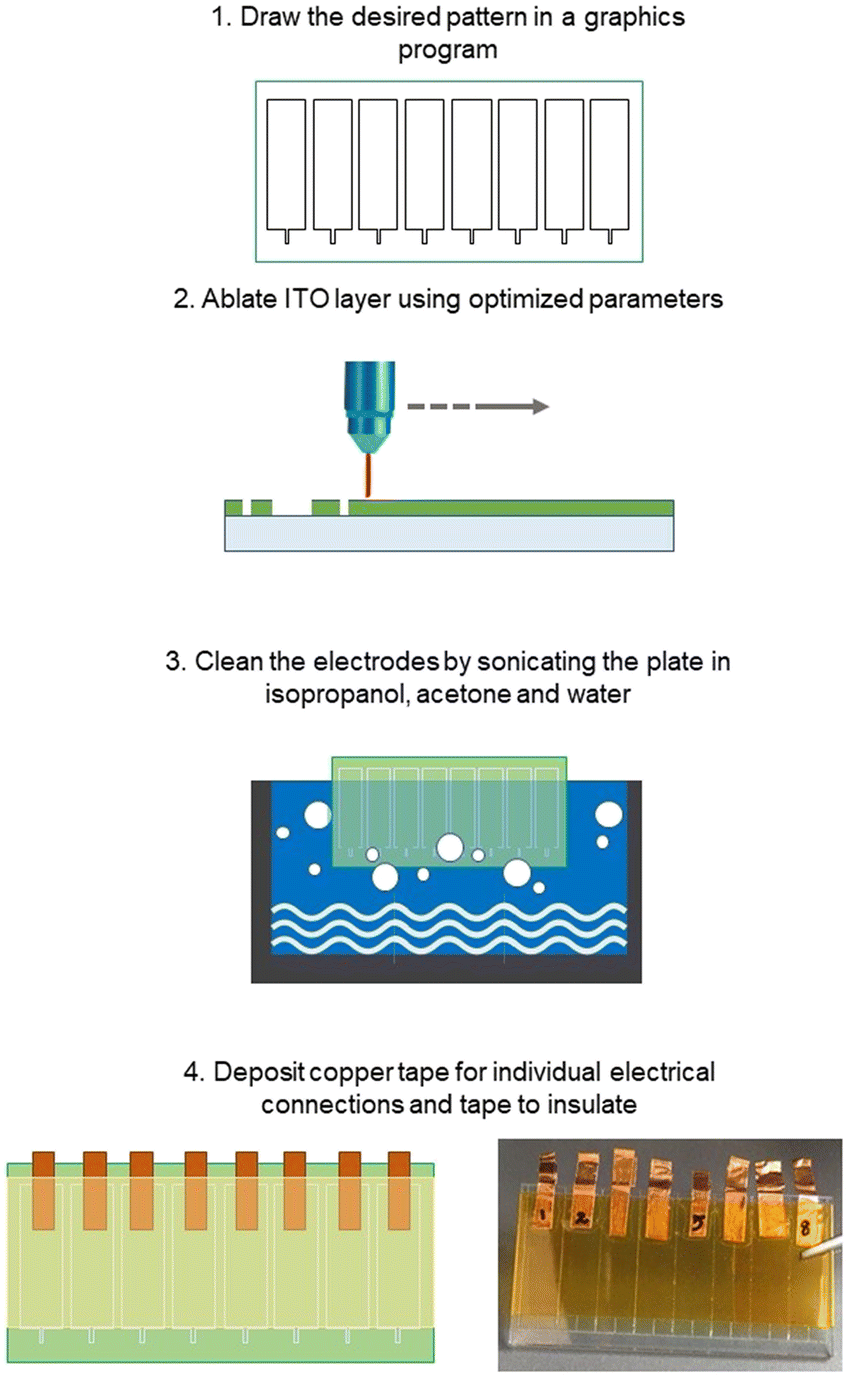 | ||
| Fig. 1 Step-by-step fabrication procedure of the directly ablated patterns. | ||
Laser ablation of scotch tape stencils and chemical etching of the ITO patterns
Clean 25 × 25 × 1.1 mm ITO covered (∼260 nm, Rs = ∼5 Ω sq−1) glass plates obtained from Biotain Crystal were covered with Scotch Magic Tape® purchased from 3 M.The same laser engraver was used to cut the tape using CAD with the following parameters: speed 3.0, power 1%, PPI 1500. After the patterning, the tape in undesired areas was removed and the plates were submerged in etchant solution (50 g FeCl3·6H2O + 80 mL distilled water + 20 mL of conc. 36% HCl) for 2.5 min at 70 °C.36 The ITO plates were then sonicated for 15 minutes each in acetone, isopropanol, and distilled water to obtain 8 clean electrodes on every plate (Fig. 2).
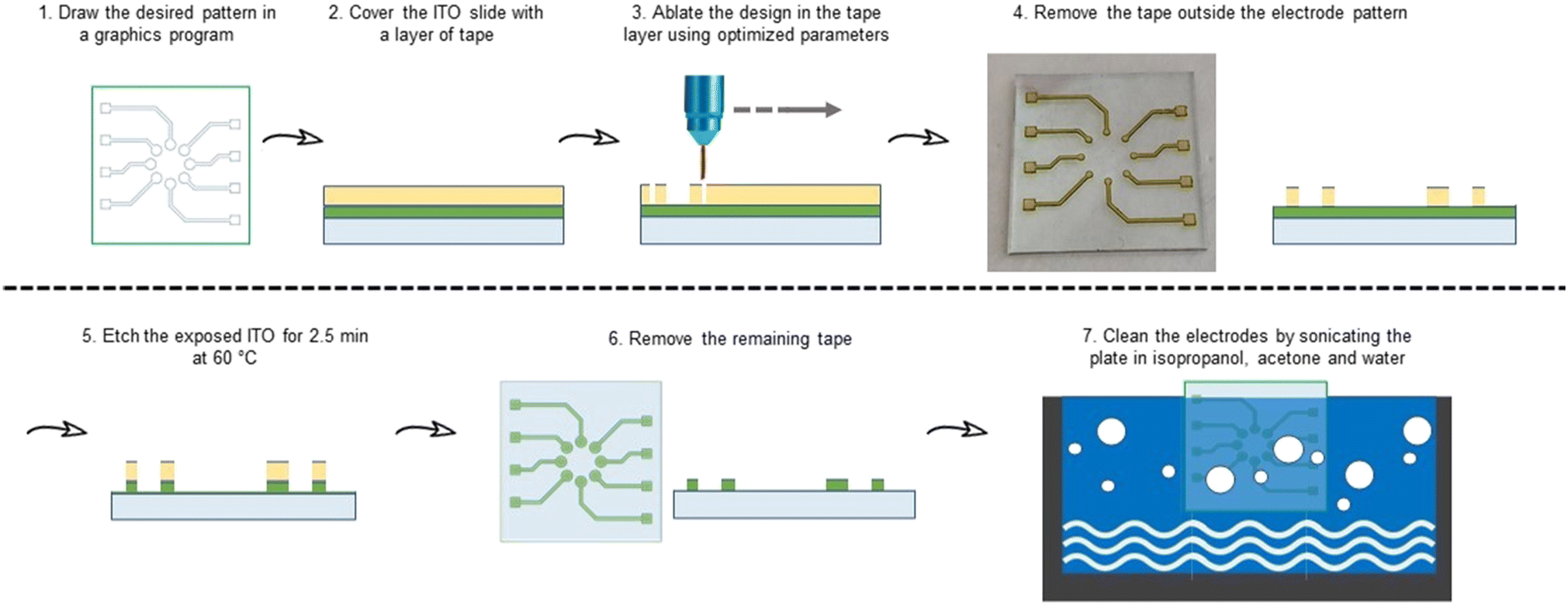 | ||
| Fig. 2 Step-by-step procedure of the electrode fabrication using laser-ablated stencils. | ||
Design of the measurement setup for the circular electrode array
The as-fabricated, 8 circular working electrodes (diameter 1.75 mm, geometrical surface area 2.41 mm2) were placed in a holder and brought into contact with a custom PCB with spring-loaded contacts, and a custom 9 mm diameter PDMS (Sylgard 184, 10:1 elastomer to curing agent ratio obtained from Dow Chemicals (Midland, MI, USA)) well was placed on top of the ITO electrode plate to prevent leakage of liquids (Fig. 3). The setup was fixed by screwing a plastic cover to the PCB together.
 | ||
| Fig. 3 Schematic representation of the measurement setup used for impedance spectroscopy of cell culture. | ||
Electrochemical measurements
All the electrochemical measurements unless stated otherwise were performed with a PalmSens 4 potentiostat/galvanostat, with an electrochemical impedance spectroscopy (EIS) module, which was controlled with PSTrace software (version 5.8.1704). The three electrode electrochemical cell consisted of a platinum wire counter electrode, Ag/AgCl (3 M KCl) reference electrode, and ITO working electrodes.The performance of the fabricated electrodes were first studied using the cyclic voltammetry (CV) technique with 1,1′-ferrocenedimethanol (FcDM) as the redox probe in 0.1 M potassium nitrate. Parameters for CV were as follows: scan rate 0.01 V s−1, step potential 0.005 V. The electrodes were cleaned first with ethanol and then with water, and dried before the measurements.
Scanning electrochemical microscopy (SECM) analysis
For all SECM experiments, carbon nanoelectrode tips were prepared according to a modified procedure described earlier in ref. 37. Acetylene gas under 1 bar of manometric pressure was used instead of a propane–butane mixture due to higher C/H stoichiometry (warning: thermal pyrolysis of acetylene at overpressures higher than 1 bar can cause an uncontrolled chain reaction and severe injury). Before imaging, the nanoelectrodes were broken in a controlled manner by approaching ITO a distance away from the intended imaging area until the desired steady-state current corresponding to the electrooxidation of ferrocenemethanol. The resulting active tip radii were estimated from steady-state currents of ferrocenemethanol oxidation at a long tip-to-sample distance. A home-build SECM setup composed of closed-loop piezo actuators (P625.2CD and P622.1CD, PI HERA with LVPZT Amplifier E-509 C3A, PhysikInstrumente) and a VA-10X patch-clamp amplifier (npi Electronic Instruments), operated under SECMx software38 through PCIDAS1602/16 analog–digital (AD) and PCI-DDA04 DA digital–analog (DA) cards (Measurement Computing), installed on top of an inverted optical microscope Nikon MA200 was used. All SECM experiments were performed in a two-electrode setup with a silver quasi-reference-counter electrode and aqueous 1 mM ferrocenemethanol in 0.1 M KCl as a mediator and supporting electrolyte, respectively. Potentiostatic polarization of the SECM tip at +0.5 V was used for a diffusion-controlled electrooxidation mediator. Samples were unbiased (floating). Imaging of activity of samples prepared by etching was performed in a constant height feedback mode, if not stated otherwise, after approaching 90% of tip current recorded at a large distance. Due to the topographic features of laser-cut ITO samples, the feedback hopping mode with a retracting distance of 10 μm was applied to record topography and activity presented as the closest distance slope of approach curves.39SEM imaging
Scanning electron microscopy (SEM) micrographs of the electrodes were captured using an FEI Nova Nano – SEM 450 with an EDAX Octane Elect Plus EDS system. EDS mapping was performed for the elements Si and In. The width of the electrodes was measured from the SEM images (see Fig. 4) using ImageJ.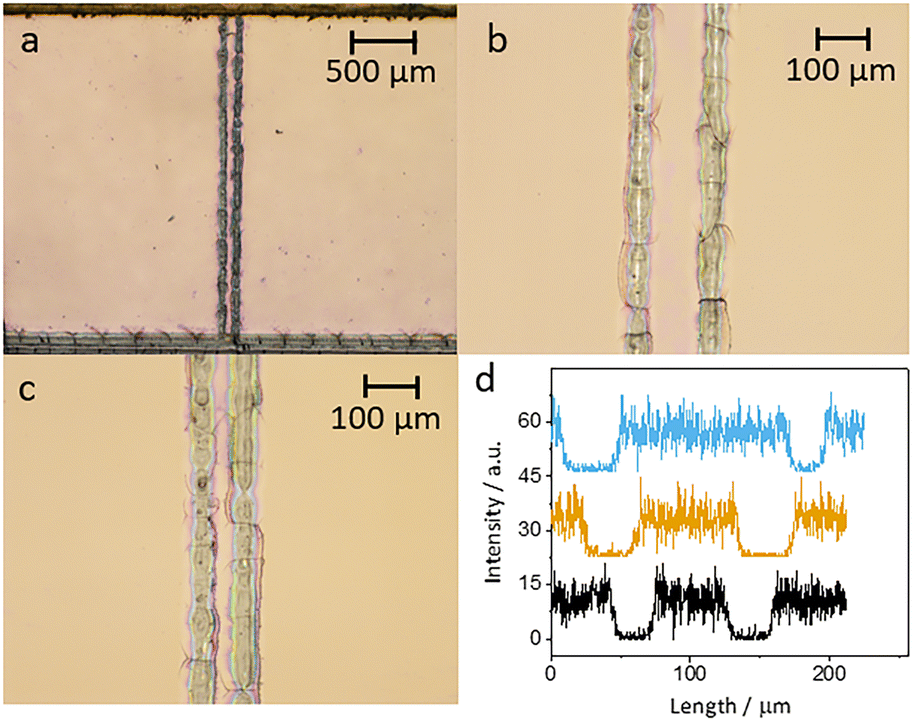 | ||
| Fig. 4 Microscopy images of an electrode with a nominal width of 100 μm at a) 2.5× magnification and b) 10× magnification, c) microscopy image of an electrode with a nominal width of 25 μm at 10× magnification, and d) EDX cross-section of the ITO electrodes depicting the intensity of indium. | ||
Optical microscopy
Qualitative analysis of the electrode structures was carried out using a Nikon ECLIPSE LV150 optical microscope. The width of the electrodes was measured and compared to the nominal width from the laser plotter.Routine cell culture
HeLa and HepG2 cell lines came from the American Type Culture Collection (ATCC, Manassas, USA). Both cell lines were cultured as a standard monolayer in the complete growth medium, supplemented with fetal bovine serum 10% v/v (FBS, Gibco), L-glutamine 1% v/v (Sigma-Aldrich), and antibiotics: streptomycin [10000 U ml−1] and penicillin [10 mg ml−1] 1% v/v (Sigma-Aldrich). Cultures were performed under standard conditions (37 °C, 5% CO2). Both cell lines were cultured in Dulbecco's modified Eagle's medium (DMEM) with a low glucose content (1 g L−1) (Institute of Immunology and Experimental Technology, Wrocław, Poland). Using regular passages, the cells were maintained in a logarithmic growth phase. To detach cells from the surface, 0.25% trypsin-EDTA solution (Sigma-Aldrich) was used.
Cell culture monitoring using impedance spectroscopy
Prior to measurements, the cells were placed at a specific density on an ITO electrode plate for cell culture monitoring utilizing impedance-based analysis. Experiments were performed in a closed, heat controlled chamber at 37 °C. A complete Dulbecco's modified Eagle's medium (DMEM), supplemented with fetal bovine serum 10% v/v (FBS, Gibco), L-glutamine 1% v/v (Sigma-Aldrich), and antibiotics: streptomycin [10000 U ml−1] and penicillin [10 mg ml−1] 1% v/v (Sigma-Aldrich), with a low glucose content (1 g L−1) (Institute of Immunology and Experimental Technology, Wrocław, Poland), suitable for HeLa and HepG2 cell lines was used.
The cells have an adhering nature. Once they attach to the working electrode surface, they tend to impede the current flow between the electrodes. This refers to the current passing through available cell–substrate space as well as through intercellular passages. When the cells approach confluence on the electrode, the impedance fluctuates visibly and changes at an accelerated rate.40
Impedance measurements were conducted over a range of 37 frequencies on HeLa cells since multiple research studies have recorded readings at various frequencies.40,41 In our case, the frequency range were set between the limits 10 Hz and 40 kHz. For frequencies between 100 Hz and 10 kHz, the data from these measurements showed a noticeable increase in the impedance modulus that corresponds to the growth of the insulating character of the electrodes due to the cells getting attached on their surface. At higher frequencies a less pronounced change is observed, with a small increase in the impedance values that can be correlated to the increase of charge transfer resistance at the working electrode–electrolyte interface. To understand the frequency that suits our measurements the best, we limited our studies to three frequencies: 100 Hz, 2 kHz, and 10 kHz. The highest phase shift and rise of the impedance values of the cells with respect to the blank (in our case DMEM) were observed at 100 Hz, thus the operating frequency was optimized as 100 Hz and all experiments were conducted at 0.2 V vs. OCP.
The majority of these measurements were brief, lasting about two hours. When the potentiostatic experiments first started, the electrode well was simply filled with 150 μL of DMEM and impedance was recorded for 30 minutes. Then, the medium in the well was spiked with 150 μL of cells with a density of 1.33 × 10⁶ cells per mL to observe their adhesion to the electrodes and how the latter's surface is affected. Finally, at the 90th minute, 150 μL of trypsin was introduced, and the system was monitored for 30 minutes more, before the impedance tests were terminated.
Results
Microscopic analysis
Initially, the electrodes were inspected using optical microscopy. At low magnification the electrodes look regular, but at higher magnification cracks and irregularities are seen, especially for the smaller electrodes (Fig. 4). Measuring the width of the electrodes shows that the narrower electrodes have uneven width ranging from 24 to 35 μm.To make sure that there was no electrical connection between the individual electrodes and other parts of the ITO plate, a negative potential of −1.5 V (vs. Ag/AgCl) was applied to the ITO working electrode for a duration of 60 seconds. This results in the reduction of the ITO layer. A significant change in the appearance of electrodes was observed, indicating disintegration of the active area to metallic indium and tin as the electrode lost its transparency and appeared darker.42 The reduced area is confined to the electrode and shows that there are no electrical connections with other parts of ITO (Fig. S8†).
The electrodes were also studied using SEM and EDX. The width of the electrodes was measured from SEM images at several positions along the length of each electrode on a plate. In Fig. S3,† we see that the widths of the electrodes, as measured by SEM, are larger than the nominal widths. In the EDX measurements, we concentrated on the elements indium and silicon. When the electrodes are cut, the EDX data clearly show that the ITO is removed along the cut. Fig. 4d shows cross sections of the indium signal for electrodes 25, 50 and 100 μm.
Electrochemistry
The ITO electrodes prepared using CO2 laser irradiation were primarily characterized using cyclic voltammetry (CV). Diffusion-controlled CVs were observed for electrodes of all the sizes within the same plate. The plate-to-plate reproducibility of signals was highly satisfactory too (14.2% for all electrodes on 5 different plates (batches)). Fig. 5 shows the cyclic voltammograms of electrodes of different sizes, where each set comes from a single plate. The lower steepness of the slope of the voltammogram and the lack of stabilization of the signal where the limiting current should be observed are indicators of resistivity of the electrode paths. The narrower the pattern the higher the influence of the resistivity of the electrode path. This effect is highly visible in the selected electrode pattern due to the high width-to-length ratio ranging from 1:100 to 1:25 for the tested designs. As the 1:25 ratio patterns already provide satisfactory results, the standard electrode, which is usually 1:1 or similar, should not be influenced by resistivity even for the smallest widths.
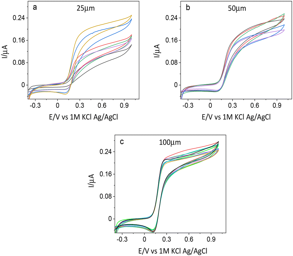 | ||
| Fig. 5 Cyclic voltammograms of electrodes of different sizes (a) 25, (b) 50 and (c) 100 μm width, 2.5 mm length in 1 mM FcDM and 0.1 M KNO3 at 100 mV s−1. Each set of electrodes comes from the same plate. | ||
Scanning electrochemical microscopy (SECM) analysis
As optical microscopy and profilometry revealed the topographic features of the laser-cut samples, constant height SECM imaging of such samples could cause SECM tip damage during imaging. Therefore, we decided to perform hopping mode feedback imaging to prevent possible crash of the SECM tip with the sample. This mode allows for high-resolution simultaneous topography and activity imaging. Lateral resolution in SECM is often limited by the probe (tip) size when the apparatus is equipped with a piezoelectric positioning system. Fig. 6 shows the topography, activity and optical images of a microband of ITO separated from the remaining part of the ITO slide by two laser-processed lines.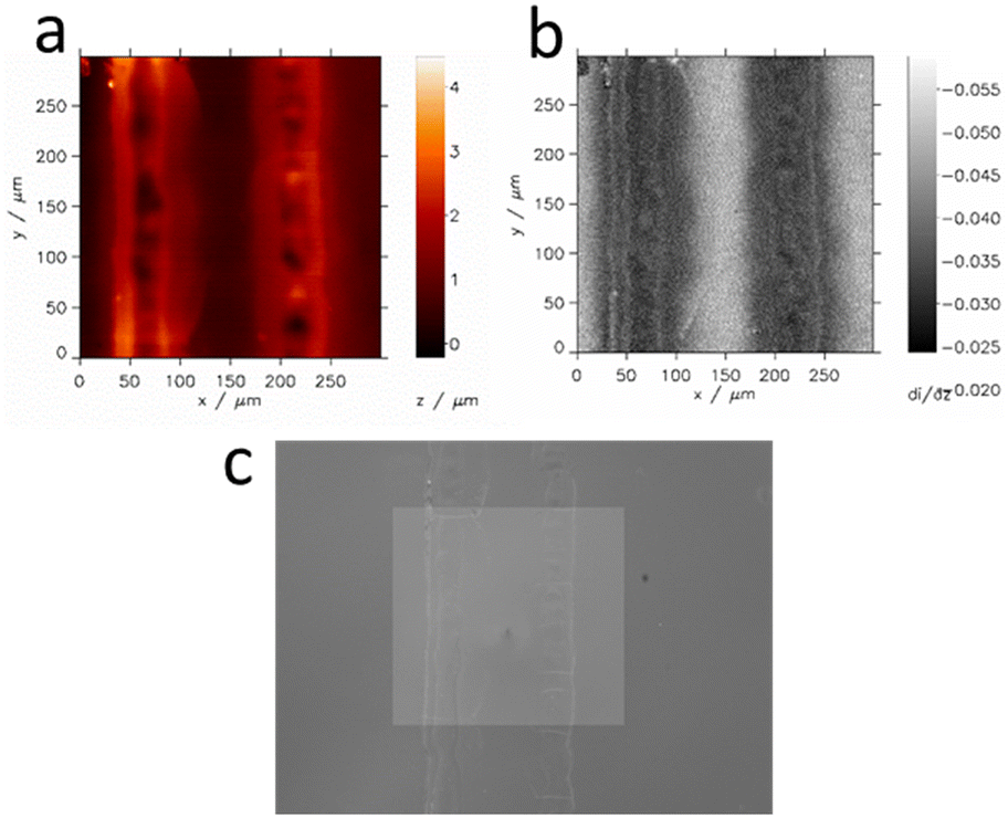 | ||
| Fig. 6 Hopping mode SECM images: topography (a), activity (b) and optical micrograph (c) of the ITO microband separated from the remaining ITO slide by laser-cutting. Scanning area: (300 × 300) μm2. The carbon microelectrode (SECM tip, Ø ca. 5.5 μm) is seen in the center of the optical image. Retracting distance: 10 μm. Effective scanning rate: 3 image pixels per second. Electrolyte: aqueous 1 mM ferrocenemethanol in 0.1 M KCl. | ||
One can see that the applied laser treatment efficiently removes ITO activity at its path. The width of deactivated ITO is irregular within ca. 60–100 μm. Therefore the ITO microband between laser paths, when their centers are 150 μm away, has a width of ca. 60–90 μm. This is not visible by optical microscopy. Optically intact parts of ITO in the vicinity of the laser paths are deactivated for charge transfer. In the center of the laser path, the sample is recessed, whereas its edges protrude up to ca. 3 μm over the ITO slide.
In the case of electrodes produced using a laser prepared stencil, selective etching of the ITO layer of ∼260 nm thickness does not cause important topographic features of the resulting sample. ITO structures do not protrude more than ∼260 nm over the glass surface. For an ∼1.3 μm radius microelectrode scanning at a distance of ca. 3.25 μm, such a sample can be considered flat enough for constant height SECM imaging. An SECM image of wider etched ITO obtained with a Ø ∼2.6 μm carbon microelectrode (Fig. S6†) reveals a slightly higher activity within a zone of ca. 30 μm width at the edge of the etched ITO. This effect can be caused by penetration of the etching solution between the ITO and deposited mask, where the etching agent removes intrinsic contamination of the ITO surface.
Reproducibility
To illustrate the variations in the current response of the electrodes, we performed cyclic voltammetry with electrodes from several batches in the redox probe FcDM. The current values of the working electrodes at the potential of 0.29 V were plotted against their sizes. The 100 μm wide electrodes had the most reproducible structures, and these electrodes, therefore exhibited the most uniform current among the three sizes, within each plate. However, their greater width also implies a higher impact of the appropriate placing of the insulation. A lower reproducibility between different batches was observed for 100 μm electrodes (Fig. 7), which can be the result of a manual error occurring during the pasting of the Kapton tape making the length of the electrodes 10 to 15% shorter or longer. The smaller sizes, 50 and 25 μm, exhibited higher intraplate variability, and this can be easily identified from Fig. 5.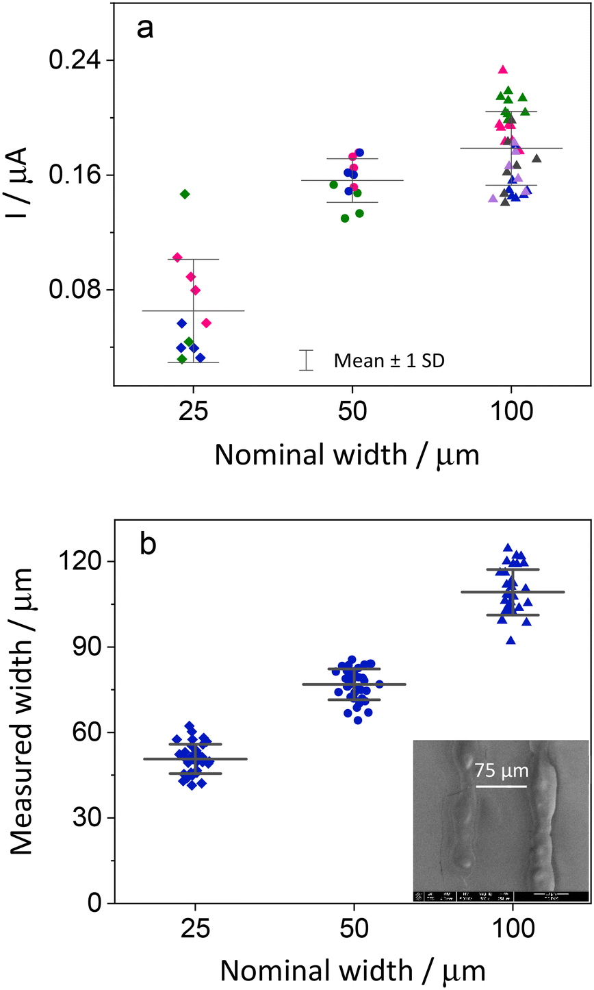 | ||
| Fig. 7 Reproducibility of electrode signals with respect to their nominal width is shown. a) The comparison of current results obtained from the cyclic voltammograms of the electrodes at 0.29 V, diamond shapes represent the 25 μm, circles the 50 μm, and triangles the 100 μm wide electrodes. Each colour represents a different ITO plate. b) The comparison of the width of the electrodes as measured by the SEM technique. The inset shows an example of an SEM image of an electrode with 50 μm nominal width. | ||
The current value does not scale with size for 50 and 100 μm wide electrodes (Fig. 7), which we initially attributed to different activities of ITO at the edges of the electrodes caused by the laser ablation. As was verified experimentally through SECM activity and topography analysis in hopping mode feedback imaging, ITO in the vicinity of the laser paths is electrochemically inactive. In this way, the actual width of the active electrodes is smaller than the one measured optically or through EDX and SEM.
A second effect, which contributes to the lack of linearity in width scaling, is caused by the ITO adjacent to larger electrodes. The adjacent ITO is not biased (floating), and remains at the open circuit potential behaving as a local concentration cell. When the product formed at the microelectrode reaches the large unconnected piece of ITO it is partially regenerated due to created concentration gradient. Because the spacing between the microelectrode and the unconnected ITO is quite narrow part of the regenerated substrate is able to reach the rectangular microelectrode thus resulting in larger current than expected from bulk concentration. The effect is more pronaunced with wider electrodes where the microelectrode widht/spacing ratio is higher.43 This effect can be eliminated through etching of the unnecessary ITO with the stencil method.
The electrodes evaluated in this work are of rectangular shape with 2.5 mm length and three different widths. These structures can also be tailored to different dimensions, for example a shorter length resulting in microelectrodes of a smaller area.
Intra- and inter-plate reproducibility is also shown in Fig. S5,† which presents current values extracted from CV measurements at a specific potential for individual electrodes from different batches (plates).
Availability
Although the proposed methods cannot compete with the use of top-end (Yb:YAG, Nd:glass, KrF) lasers in terms of the smallest possible pattern or line width (Table S1†), they can be used with a very low investment in the equipment or even using external resources. Laser plotters as the ones used in this work are quite often used in printing shops for preparation of stamps, cutting and engraving. We have prepared a few batches of electrodes using both methods in a local printing shop. Power settings needed to be adjusted and a few of the structures had imperfections in the cut which could be probably reduced after cleaning of the optics, but we were still able to fabricate structures of similar electrochemical performance (Fig. S7 and S8†).Impedance measurements
Circular electrode geometries are recommended for applications that involve observation of a section of a volume (such as in the medical field).44,45 Therefore, for our cell culture studies, we implemented a second method to develop an electrode array in a circular geometry (each array consists of equally spaced 8 identical electrodes). Moreover, circular electrodes in such an array provide a symmetric electric field distribution due to an evenly distributed electrode layout. This uniformity is crucial for consistent and controlled electrical interactions with the surrounding medium and cells.The stability of the system was assured by conducting potentiostatic reading at a fixed potential against open circuit potential (OCP). The first 30 min duration was measured with only DMEM in the well, which was then spiked with HeLa cells, and their attachment to the electrodes was observed for 60 minutes. Later, trypsin was introduced to the well in order to track the detachment or separation of these cells from the electrodes and studies were continued for an additional 30 minutes. Current or voltage applied to the setup in the absence of cells with only the medium as an electrolyte reflects the interfacial impedance in series with ionic conductivity of the solution.
As anticipated, our results showed lower impedance and a slower growth pattern during the first 30 minutes of recording compared to the growth while the cells were making close contact with the electrode surface. This attachment of the cells provides an additional hindrance to alternating current flow apart from the solution resistance. The resultant output is a combination of resistive and capacitive elements. While the insulating cell membranes are responsible for the capacitive effects, the resistive effect is due to the ionic properties of cytoplasm.41 Although inspection of cell responses for 30 minutes after the addition of trypsin did not completely remove them from the substrate contact, reducing the cell layer resistance to the point where the final signal resembled those throughout the absence of cells, it was evident that within this short period of time a considerable portion of the cells was successfully detached from the electrode contact.
The responses of HepG2 cells were also studied through recording impedance alteration over time. It was noted that the resistance component Z′ does not change significantly because there are still noticeable intercellular voids. The HepG2 cells form spheroids on the surface of culture vessels rather than confluent layers as HeLa cells. With this cell population, the adherence interaction did not appear to be strong enough to give considerable change in Z′. However, when it comes to the capacitance component, Z′′, accountable changes can be seen within the measurement conditions. Thus, the Z′′ element validates to be a more dependable variable for us. Fig. 8 shows the real-time monitoring of the impedance evaluations for 2D HepG2 cell culture. Comparable signals were obtained from all 8 electrodes.
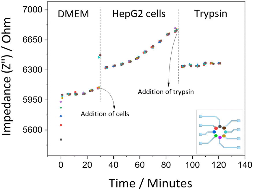 | ||
| Fig. 8 Impedance recording of HepG2 cell culture measured at 100 Hz showing cell adhesion and detachment (short-term measurements lasting for 2 hours). Each color represents a different electrode. | ||
Conclusions
The objective of this work was low-cost fabrication of ITO electrodes through a novel laser assisted method. We successfully optimized the cutting of ITO coated glass plates into functional electrodes with a CO2 laser. The electrodes of different shapes and sizes were prepared using two different methods. For the smaller rectangular shaped microelectrodes (the smallest nominal widths optimized were 25, 50 and 100 μm wide), direct patterning was used, while in situ stencil fabrication followed by etching was observed as the best practice for the larger circular shaped electrodes (diameter 1.75 mm, geometrical surface area 2.41 mm2). Direct laser ablation allows smaller features to be fabricated, but the electrodes suffer from damage at the edges, which results in reduced electroactive area as compared with the widths measured with optical microscopy, SEM or EDX (∼80 μm width active for charge transfer for 100 μm wide structures). The second method in which a laser is used to ablate the stencil deposited on ITO leads to structures of larger footprint (min. feature size ∼100 μm) but does not damage the edges. Together both methods form a toolbox that allows small structures to be fabricated through direct ablation and removal of ITO from larger surfaces through the stencil method.All the electrodes and electrode arrays thus fabricated demonstrated stable and reproducible signals, with an average standard deviation for current for 100 μm wide patterns being 7.8% within a single plate and 14.2% for all electrodes on 5 different plates (batches) (Fig. S5†). Single electrodes were used repeatedly for several months and did not show deterioration of signals over time. The cost-effective, easily fabricated, simple, and handy ITO electrodes we presented here can be treated as any contemporary working electrode in use and as a tool in several fields like sensing, bio-sensing, EWOD, microfluidics, cell culture studies and much more. As a demonstration, we used the electrode arrays for cell culture characterization using electrochemical impedance spectroscopy (EIS).
Author contributions
KKV – investigation, formal analysis, writing – original draft; MSF – investigation, methodology; WR – investigation; EJ – investigation; MJN – conceptualisation, methodology, investigation, formal analysis, writing – review & editing, supervision; WN – investigation (SECM), EWN – conceptualisation, methodology, investigation, writing – review & editing, supervision, funding acquisition.Conflicts of interest
There are no conflicts to declare.Acknowledgements
EWN, KKV, and EJ thank the National Centre for Research and Development, Poland, for funding under grants LIDER/38/0138/L-9/17/NCBR/2018. MSF acknowledges that this publication is part of a project that has received funding from the European Union's Horizon 2020 research and innovation programme under the Marie Skłodowska-Curie grant agreement no. 847413. Scientific work published as part of an international co-financed project founded from the programme of the Minister of Science and Higher Education entitled “PMW” in the years 2020–2024; agreement no. 5005/H2020-MSCA-COFUND/2019/2. WR thanks Norway Grants 2014–2021 via the National Centre for Research and Development (NOR/POLNOR/UPTURN/0060/2019). We thank the local printing shop “STARCOM, P.H.U. 26-800 Białobrzegi, ul. Kościelna 48” for helping us prepare a batch of electrodes using their CO2 laser plotter. We would like to also acknowledge Ms Zuzanna Zambrowska who fabricated the first few sets of laser etched ITO electrodes.References
- A. Stadler, Materials, 2012, 5, 661–683 CrossRef PubMed.
- E. B. Aydın and M. K. Sezgintürk, TrAC, Trends Anal. Chem., 2017, 97, 309–315 CrossRef.
- C. G. Granqvist and A. Hultåker, Thin Solid Films, 2002, 411, 1–5 CrossRef CAS.
- H. B. Lee, W. Y. Jin, M. M. Ovhal, N. Kumar and J. W. Kang, J. Mater. Chem. C, 2019, 7, 1087–1110 RSC.
- Z. Zhuang, D. Iida, P. Kirilenko, M. Velazquez-Rizo and K. Ohkawa, Opt. Express, 2020, 28, 12311–12321 CrossRef CAS PubMed.
- J. Chinky, P. Kumar, V. Sharma, P. Malik and K. K. Raina, J. Mol. Struct., 2019, 1196, 866–873 CrossRef.
- G. Lucarelli and T. M. Brown, Front. Mater., 2019, 6, 1–11 CrossRef.
- M. Si, J. Andler, X. Lyu, C. Niu, S. Datta, R. Agrawal and P. D. Ye, ACS Nano, 2020, 14, 11542–11547 CrossRef CAS PubMed.
- J. Y. Zhou, J. L. Bai, H. Zhao, Z. Y. Yang, X. Y. Gu, B. Y. Huang, C. H. Zhao, L. Cairang, G. Z. Sun, Z. X. Zhang, X. J. Pan and E. Q. Xie, Sens. Actuators, B, 2018, 265, 273–284 CrossRef CAS.
- X. Huang, W. Shi, J. Li, N. Bao, C. Yu and H. Gu, Anal. Chim. Acta, 2020, 1103, 75–83 CrossRef CAS PubMed.
- S. Sharma, A. Kumar, N. Singh and D. Kaur, Sens. Actuators, B, 2018, 275, 499–507 CrossRef CAS.
- A. Celebanska, M. S. Filipiak, A. Lesniewski, E. Jubete and M. Opallo, Electrochim. Acta, 2015, 176, 249–254 CrossRef CAS.
- D. Zhang, A. Tavakoliyaraki, Y. Wu, R. A. C. M. M. van Swaaij and M. Zeman, Energy Procedia, 2011, 8, 207–213 CrossRef CAS.
- K. A. Sierros, N. J. Morris, K. Ramji and D. R. Cairns, Thin Solid Films, 2009, 517, 2590–2595 CrossRef CAS.
- I. Baía, M. Quintela, L. Mendes, P. Nunes and R. Martins, Thin Solid Films, 1999, 337, 171–175 CrossRef.
- G. Singh, H. Sheokand, S. Ghosh, K. V. Srivastava, J. Ramkumar and S. A. Ramakrishna, Appl. Phys. A: Mater. Sci. Process., 2018, 125, 23 CrossRef.
- S. Pratheesh Kumar, S. Elangovan, R. Mohanraj and V. Sathya Narayanan, Mater. Today: Proc., 2021, 46, 8086–8096 CrossRef CAS.
- E. Assuncao and S. Williams, Opt. Lasers Eng., 2013, 51, 674–680 CrossRef.
- Handbook of Manufacturing Engineering and Technology, ed. A. Y. C. Nee, Springer London, London, 2015 Search PubMed.
- V. B. Nam, T. T. Giang, S. Koo, J. Rho and D. Lee, Nano Convergence, 2020, 7(1), 23 CrossRef CAS PubMed.
- J. H. Kim, K. A. Jeon, G. H. Kim and S. Y. Lee, Appl. Surf. Sci., 2006, 252, 4834–4837 CrossRef CAS.
- N. Mokhtarifar, F. Goldschmidtboeing and P. Woias, J. Electrochem. Soc., 2019, 166, B896–B902 CrossRef CAS.
- H. M. Reinhardt, P. Maier, H. C. Kim, D. Rhinow and N. Hampp, Adv. Mater. Interfaces, 2019, 6, 1–6 Search PubMed.
- M. Kundys, M. Nejbauer, M. Jönsson-Niedziolka and W. Adamiak, Anal. Chem., 2017, 89, 8057–8063 CrossRef CAS PubMed.
- W. Chen, P. Ackerson and P. Molian, Mater. Des., 2009, 30, 245–251 CrossRef CAS.
- H.-B. Liu and H.-Q. Gong, J. Micromech. Microeng., 2009, 19, 037002 CrossRef.
- N. C. Speller, G. G. Morbioli, M. E. Cato, T. P. Cantrell, E. M. Leydon, B. E. Schmidt and A. M. Stockton, Sens. Actuators, B, 2019, 291, 250–256 CrossRef CAS.
- V. Radonić, S. Birgermajer, I. Podunavac, M. Djisalov, I. Gadjanski and G. Kitić, Electronics, 2019, 8(12), 1475 CrossRef.
- G. Chitnis, Z. Ding, C. L. Chang, C. A. Savran and B. Ziaie, Lab Chip, 2011, 11, 1161–1165 RSC.
- M. Rashiku and S. Bhattacharya, in Paper Microfluidics, 2019, pp. 29–45 Search PubMed.
- T. Pinheiro, S. Silvestre, J. Coelho, A. C. Marques, R. Martins, M. G. F. Sales and E. Fortunato, Adv. Mater. Interfaces, 2021, 8, 2101502 CrossRef CAS.
- B. Kulyk, B. F. R. Silva, A. F. Carvalho, S. Silvestre, A. J. S. Fernandes, R. Martins, E. Fortunato and F. M. Costa, ACS Appl. Mater. Interfaces, 2021, 13, 10210–10221 CrossRef CAS PubMed.
- S. Deshmukh, P. Jakobczyk, M. Ficek, J. Ryl, D. Geng and R. Bogdanowicz, Adv. Funct. Mater., 2022, 32, 2206097 CrossRef CAS.
- L. Ge, Q. Hong, H. Li, C. Liu and F. Li, Adv. Funct. Mater., 2019, 29, 1–10 Search PubMed.
- Q. Hassan, S. Ahmadi and K. Kerman, Micromachines, 2020, 11(6), 590 CrossRef PubMed.
- On the Mechanism of ITO Etching: The Specificity of Halogen Acids, IOPscience, https://iopscience.iop.org/article/10.1149/1.2221071, (accessed July 10, 2023) Search PubMed.
- M. Michalak, M. Kurel, J. Jedraszko, D. Toczydlowska, G. Wittstock, M. Opallo and W. Nogala, Anal. Chem., 2015, 87, 11641–11645 CrossRef CAS PubMed.
- C. Nunes Kirchner, K. H. Hallmeier, R. Szargan, T. Raschke, C. Radehaus and G. Wittstock, Electroanalysis, 2007, 19, 1023–1031 CrossRef.
- J. Jedraszko, M. Michalak, M. Jönsson-Niedziolka and W. Nogala, J. Electroanal. Chem., 2018, 815, 231–237 CrossRef CAS.
- S. Ramasamy, D. Bennet and S. Kim, Int. J. Nanomed., 2014, 9, 5789–5809 CAS.
- A. R. A. Rahman, J. Register, G. Vuppala and S. Bhansali, Physiol. Meas., 2008, 29, S227 CrossRef CAS PubMed.
- L. Liu, S. Yellinek, I. Valdinger, A. Donval and D. Mandler, Electrochim. Acta, 2015, 176, 1374–1381 CrossRef CAS.
- T. Horiuchi, O. Niwa, M. Morita and H. Tabei, J. Electrochem. Soc., 1991, 138, 3549 CrossRef CAS.
- J. Padilha Leitzke and H. Zangl, Sensors, 2020, 20, 5160 CrossRef PubMed.
- M. Schwarz, M. Jendrusch and I. Constantinou, Electrophoresis, 2020, 41, 65–80 CrossRef CAS PubMed.
Footnote |
| † Electronic supplementary information (ESI) available. See DOI: https://doi.org/10.1039/d3lc00266g |
| This journal is © The Royal Society of Chemistry 2023 |