
 Open Access Article
 This Open Access Article is licensed under a Creative Commons Attribution-Non Commercial 3.0 Unported Licence
A chemist's guide to photoelectrode development for water splitting – the importance of molecular precursor design
Thom R.
Harris-Lee
 ab,
Frank
Marken
a,
Cameron L.
Bentley
b,
Jie
Zhang
*b and
Andrew L.
Johnson
*a
ab,
Frank
Marken
a,
Cameron L.
Bentley
b,
Jie
Zhang
*b and
Andrew L.
Johnson
*a
aDepartment of Chemistry, University of Bath, Claverton Down, Bath, BA2 7AY, UK. E-mail: chsalj@bath.ac.uk
bSchool of Chemistry, Monash University, Clayton, Vic 3800, Australia. E-mail: jie.zhang@monash.edu
First published on 21st September 2023
Abstract
Photoelectrochemical (PEC) water splitting is a promising method for generating green hydrogen as a solar fuel, overcoming the issues associated with unreliability and periodicity of renewable technologies. While research in this field is growing, there is a distinct gap between complex device development and fundamental synthesis of the individual materials. For optimal device fabrication we need materials scientists and engineers to create complex multicomponent photoelectrodes, but also inorganic chemists to design bespoke precursors tailored to produce highly efficient, specifically designed photoelectrode materials. The success of precursor design for semiconductors in fields such as microelectronics has proven the significant impact of the precursor, however, this approach has yet to be used extensively in device fabrication for PEC water splitting. This review acts as a guide towards bespoke precursor development for the fabrication of tailored thin films; particularly how to design the structure and composition of the precursor to promote and enhance the most desired properties, including solubility, volatility, and thermal decomposition. The key areas of focus for device design are outlined, including both single thin film performance and overall device modifications and additions to create a high-performance PEC water splitting electrode. There is a specific emphasis towards chemical vapour deposition techniques due to the suitability for scale-up and commercial application compared to alternatives, and importantly, the significant influence of the molecular precursor on the deposition, and hence its link to synthetic chemistry. We aim to direct more synthetic chemists towards the field of PEC water splitting, encouraging collaboration to connect these two areas and bring the target of a commercially and industrially viable PEC system ever closer.
Broader contextRenewable technologies are contributing more towards global electricity production each year; however the intermittency and periodicity of renewable energy supply prevents these technologies from completely replacing fossil fuels unless a suitable method for energy storage is available. Storage of energy as hydrogen, one of the most promising fuels for the future, through coupling photovoltaics with electrolysis (PV–E) is the most technologically-ready green hydrogen production method, however the current technology relies on the use of high-cost crystalline silicon for light harvestings. Direct water splitting through photoelectrochemical catalysis (PEC) or photocatalysis (PC), which utilise low grade and hence low-cost semiconductors, is therefore seen as the ultimate target, however its low technological readiness level means research should focus on improving the overall device fabrication and optimisation process. One significant part of the fabrication process that is mostly ignored is the bespoke design of precursors to tailor towards desired thin film properties. This review acts as a guide towards how precursors can be specifically designed to make effective water splitting photoelectrodes from a molecular chemistry bottom-up approach, encouraging a more interdisciplinary method towards efficient PEC water splitting, and promoting collaboration and a greater involvement of inorganic chemists into this expanding and essential field of research. |
1. The need for photoelectrode materials in the hydrogen economy
The urgent need to combat climate change and environmental pollution through the transition from fossil-based to renewable energy sources is more apparent than ever. However, while the use of renewables is at an all-time high, it is still dwarfed by the consumption of oil, coal, and natural gas.1 The solar energy available for harnessing at the Earth's surface far surpasses the global energy demand,2 however, it is not possible for solar energy to replace fossil fuels without viable methods of long-term energy storage. The intermittent and unreliable nature of solar power results in peak production and peak demand rarely being aligned, both on a short term (day/night cycle) and long term (seasonal) period. There is therefore an essential requirement to store excess energy, which can then be transported and conveniently converted back into electricity when demand exceeds production.Batteries are an obvious candidate for storage given their high round-trip efficiencies and technological readiness level, but unfortunately are unsuited to long-term storage for large-scale energy production due to their high running costs, large required facility size, significant charge leakage over long time periods, and issues associated with the recycling of potentially toxic, explosive, and environmentally damaging elemental components at end of life.3,4 Further, the cost of lithium-ion batteries, the current standard in battery technologies, is high and constantly increasing, with a predicted shortage of lithium and other transition metal constituents in the future.5 Finally, the storage capacity of batteries is currently insufficient for large scale operations such as grid-level storage, as limitations are already commonly encountered in relatively small-scale operations such as the travel range of electric vehicles.6
The production of solar fuels represents an alternative storage method whereby energy is stored in chemical bonds, which can be converted back to electricity directly using a fuel cell.7 Solar radiation can be converted directly into a solar fuel via photoelectrochemical (PEC) catalysis and photocatalysis (PC), or indirectly via photovoltaics coupled to electrolysis (PV–E). Direct conversion has the potential for greater efficiency due to lower material costs and intrinsic thermal management, however, it currently has a far lower technological readiness level.
Among the range of possible solar fuel options, hydrogen is the most promising for a fully sustainable system due to its large energy density by weight (142 MJ kg−1, 3 times larger than gasoline),8 sourcing from water, as well as many other potential feedstocks, and zero emissions at point of use, with oxygen and water the only by-products upon hydrogen generation and back conversion into electricity respectively.9 However, despite its foremost energy density by weight compared to alternatives, hydrogen has the lowest energy density by volume of all common fuels, meaning storage and transport are challenging aspects for creating an economy that uses hydrogen as a fuel.10 Comparisons between hydrogen and current standard fossil and biofuels for energy densities by weight and volume are shown in Fig. 1.
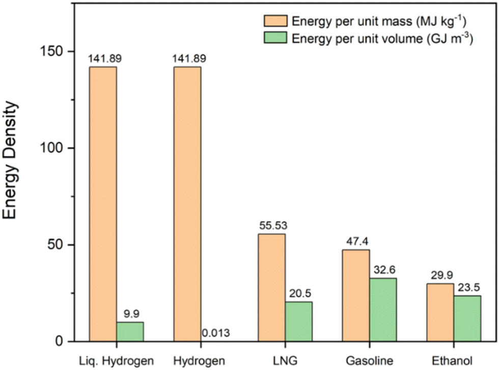 | ||
| Fig. 1 Comparison between the energy density by weight and energy density by volume of hydrogen and common standard fuels. Data obtained from ref. 11. | ||
Industrial hydrogen production presently relies on fossil fuels via steam methane reforming due to the low cost per kg, in comparison to green hydrogen alternatives. It is therefore important to consider how PV–E, PEC, and PC methods can be made more economically efficient.12 Certain PEC anode materials can selectively oxidise a non-water/hydroxide species, while the cathode still evolves hydrogen, a common example of this being the oxidation of chloride ions to chlorine gas and hypochlorite ions, products used in disinfectant production.13 Producing important commercial products required in large scales at both electrodes (rather than oxygen at the anode, as in conventional PEC water splitting) without increased equipment or running costs would further increase the economic viability of PEC,14,15 and reduce the significant price gap between solar hydrogen production and fossil fuel methods.12
PEC water splitting is a multi-disciplinary topic that has been the subject of many reviews, ranging from in-depth studies of photoelectrode materials and properties, to the photophysical processes that occur, to political and socio-economic implementation strategies.4,16–26 One major gap that has not been addressed is the nature of material fabrication, specifically the use of novel molecular precursors systematically designed for the deposition of designer PEC electrode materials. At present, it is commonplace to use readily available precursors that are not tailored for the deposition of PEC materials specifically. While some highly performing electrodes have been reported using this approach, there is also an abundance of poor or average performing electrodes, and the information gained towards future photoelectrode development from such an approach is limited. This review will discuss how to design bespoke molecular precursors for a systematic and informed approach to photoelectrode design, targeting both the structural precursor properties that promote effective use in deposition techniques, and the resulting deposited film properties that are known to enhance PEC performance.
2. Fundamental aspects of photoelectrodes
2.1 Photoelectrochemical water splitting
PEC devices split water in a two-step process: (1) photoabsorption followed by (2) redox catalysis. These steps can either both occur in a single semiconducting material, or be split among different distinct materials deposited onto one another. A typical PEC setup (Fig. 2a) consists of an anode and a cathode, where either one or both will be photoactive. When sunlight is incident on a photoelectrode, photons with an energy equal to or greater than the bandgap of the material are absorbed, causing excitation of an electron (e−) from the valence band (VB) into the conduction band (CB), leaving behind a hole (h+). The electron and hole are still in a ‘pair’, each feeling the others attractive influence, favouring recombination to return to the lower energy state of electron in the VB. The time duration before this recombination event occurs is known as the excited state lifetime, which must be greater than the total time required for consumption of the charge carriers in the water splitting reaction, otherwise no charge carriers will be available for use in this redox process.22,24,26–28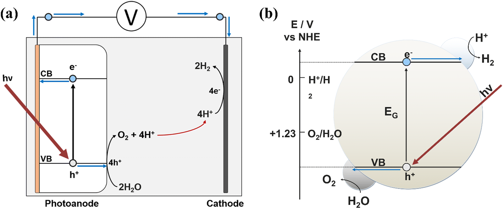 | ||
| Fig. 2 Schematics depicting (a) a simple photoanode-based PEC device, and the redox processes occurring at each electrode after photon absorption, and (b) a PC nanoparticle with both HER and OER taking place, where hν ≥ EG. | ||
To improve the efficiencies of charge carrier separation and interfacial charge transfer, a bias potential can be applied to the system. In a photoanode, the photoexcited electrons transport to the conductive back-contact where they leave the anode and flow to the cathode, while the holes diffuse to the electrode–electrolyte interface where they are consumed for use in oxidation reactions. Ideally, photo-water splitting would operate without the application of an external bias potential (i.e. a PC device), for example, using freely suspended semiconducting particles with loaded electrocatalysts that facilitate both the oxygen evolution reaction (OER) and hydrogen evolution reaction (HER) simultaneously from the photo-generated holes and electrons respectively, depicted in Fig. 2b. While developments in photoelectrodes for PEC are discussed herein, the methods could also apply to a PC device.
During water splitting, four photons are required for every oxygen molecule, and every two hydrogen molecules, evolved. The reactions taking place at each electrode are:
| Photoelectrode 4hν → 4h+ + 4e− | (1) |
| Anode 2H2O + 4h+ → 4H+ + O2↑ | (2) |
| Cathode 4H+ + 4e− → 2H2↑ | (3) |
| Overall 2H2O + 4hν → O2↑ + 2H2↑ | (4) |
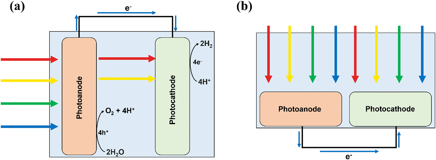 | ||
| Fig. 3 Schematics showing PEC setups for (a) conventional tandem and (b) parallel configurations. | ||
There are 5 main parameters that should be investigated to determine the efficiency of a PEC cell: (i) photon absorption; (ii) electron–hole pair separation; (iii) carrier diffusion/transport; (iv) catalytic efficiency; (v) mass transfer of reactant/product (e.g. the electrolyte ions, O2 and H2 gas etc.). The first 4 parameters all contribute towards the available charge carrier density, which is the abundance of charge carriers produced by the device that are available for use in water splitting.21
One major hurdle for PEC research is its difficulty in reproducibility due to the abundance of variables that can have significant impact on any of the parameters listed above, and hence the overall device activity and efficiency.32 Research must, therefore, strictly control all variables that can be reasonably controlled (e.g. annealing conditions, accidental dopant/impurity addition, and synthesis/deposition protocols etc.) to reduce the impact of those that are more difficult to control.
2.2 Semiconductor energy bands
The detailed physics of how semiconductor bands function and behave is beyond the scope of this review, however, the most important fundamentals are covered, and for additional information the reader is directed to ref. 33–36.The energy difference between the VB and CB (analogous to highest occupied molecular orbital (HOMO) and lowest unoccupied molecular orbital (LUMO) respectively for the case of a single molecule) must be smaller than or equal to the energy of an incident light photon to generate an electron–hole pair. In the solar spectrum at the Earth's surface, UV radiation (up to 380 nm, ∼3.26 eV) makes up a maximum of 3.3%, compared to visible light (380–800 nm, 3.26–1.55 eV) which can reach values >35% on clear days.21,37 Thus, even an electrode that absorbs up to 600 nm (2.07 eV) in the visible spectrum will still only be accessing 17.8% of the total incident radiation.38
Note that infrared radiation is generally not considered for absorption in PEC water splitting despite its >50% composition in the solar spectrum. This is because PEC water splitting requires a minimum bandgap of at least 1.23 eV, or more realistically of ∼1.5 eV, to overcome the separation between the H+/H2 and O2/H2O redox potentials, which is not possible with infrared light.39,40 In other words, for water splitting to occur on a single semiconducting material, the CB must be positioned more negatively than the H+/H2 reduction potential such that it will donate electrons to H+ ions. Additionally, the VB must be positioned more positively than the O2/H2O potential for photogenerated holes in the semiconductor to oxidise H2O.26
Fig. 4 presents cases where different semiconductors have band positions allowing (a) both HER and OER, (b) only HER, (c) only OER.41 In the case where only one of the redox reactions can occur, it is possible for high performance electrocatalysts with a more suited energy level to be deposited onto the surface of the photocatalyst, thus separating the photoabsorption and electrocatalysis processes between two components of an overall photoelectrode (rather than a single semiconducting film providing both functions).42,43 A photoelectrode material only requires band positions suitable for both OER and HER if it is to be used as both the photoanode and photocathode, or as a photocatalyst. If the semiconductor will only be used as a photoanode, it only needs a suitable valence band maxima (VBM) position, and similarly for a photocathode, only the conduction band minima (CBM) must be located at a suitable relative energetic position. The relative positions of the CBM and VBM are also important for heterojunction formation (Section 6.1).
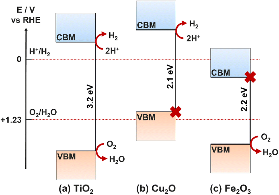 | ||
| Fig. 4 Bandgap energy levels for three semiconductor examples at pH 0 relative to HER and OER redox potentials. (a) TiO2 electrode: both HER and OER allowed, (b) Cu2O electrode: HER allowed, OER forbidden, (c) Fe2O3 electrode: HER forbidden, OER allowed. | ||
Bandgap size is one of the most significant influences on the PEC activity for a single material, for example, TiO2 is one of the most promising semiconductors for water splitting applications, however, its large bandgap (3–3.2 eV) limits its use to multi-component devices, where photon absorption can be achieved through other semiconductor layers or sensitizers.44 Tuning the bandgap is challenging, and can only reliably be achieved for a given material using dopants, which introduce dopant energy levels between the CB and VB of the bulk material, hence increasing the charge carrier density and decreasing the minimum energy required for exciton generation (Section 4.3). Combining multiple materials of different bandgaps in tandem is another effective method for increasing the efficiency of charge carrier generation, maximising photon absorption and minimising efficiency loss due to vibrational relaxation after high energy (relative to the band gap) electron excitations.45
Semiconductors can exist as either p-type or n-type depending on whether the majority charge carriers are holes or electrons, respectively. An excess of one charge carrier can be formed intrinsically by lattice vacancies, or extrinsically by substitution of lattice atoms with dopant atoms, hence p-type and n-type semiconductors can be manufactured by doping with atoms that act as electron acceptors or electron donors relative to the initial lattice. In silicon (Si) for example, n-type Si can be produced by substituting Si atoms in the lattice with phosphorous (P). The excess electron in each P atom will orbit the dopant atom with low binding energy such that it can be readily removed by thermal fluctuations and promoted to the CB to produce an electron excess. The vacuum level of the dopant is therefore set as the CBM of the semiconductor, resulting in the donor ground state being positioned just below the CB (Fig. 5). The reverse is true to p-type Si, doping with a relatively electron deficient atom, such as aluminium, forms a dopant energy level at an energy above the VBM equal to the binding energy of the weakly bound orbiting hole, resulting in electron deficiency, or hole excess.33,46
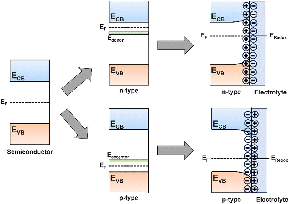 | ||
| Fig. 5 Schematic showing the bandgap for a pure semiconductor, Fermi levels in n- and p-type semiconductors, and the origin of band bending when a semiconductor is put in contact with an electrolyte. | ||
So far, this section has assumed an isolated semiconductor, whereas in a real PEC system the semiconductor is in contact with an electrolyte, which itself has a specific redox potential (Eredox). In the case of ‘flat bands’ as described so far, the Fermi level (EF), the energy at which there is a 50% probability of a state being occupied, is exactly halfway between the full VB and empty CB. In this case, when an electron–hole pair is generated by photon absorption, and no intrinsic electric field exists to drive carriers towards the semiconductor interface, rapid nonradiative recombination will occur, giving rise to no photocurrent. Upon immersion of the semiconductor in an electrolyte, the difference between EF and Eredox results in a transfer of electrons across the interface, forming a depletion on one side and excess on the other – an electric field is formed within the near-surface region of the semiconductor, known as a space-charge region.
For n-type semiconductors, EF will be greater than Eredox, hence electrons will transfer from higher to lower energy by injection from the semiconductor into the electrolyte, forming an electron depletion layer which forces an upward bending of the bands, decreasing EF to the value of Eredox and forming an equilibrium (Fig. 5). The opposite is true for p-type semiconductors, where an electron accumulation layer will bend bands downwards. Now, when an electron–hole pair is generated within the space-charge region, the intrinsic electric field will drive the carriers either towards or away from the interface, promoting mobility and facilitating catalysis at the surface. Any carriers generated within the bulk of the semiconductor, unaffected by the space-charge field, will move slowly, by only diffusion due to the absence of any electric field influence, towards the electrolyte interface or conductive back contact.
The amount of band bending can be controlled through the application of a bias potential, which shifts the Fermi level. The band energy within the bulk of the semiconductor (outside the depletion region) can shift with applied potential, but the degree of band bending will vary to compensate for this shift, maintaining the same band edge positions relative to the redox potentials of the electrolyte. The application of a bias potential therefore increases the efficiencies of charge carrier separation and interfacial charge transfer, but does not alter the band gap or band edge positions.36
2.3 Performance indicators for photoelectrochemical cells
Quantitative PEC data is required for determining the relative performance of an electrode, and standard measurements allow for effective comparison between reports. This chapter covers the most essential benchmarking metrics to effectively evaluate PEC performance, requiring minimal specialist equipment or training. It should be noted that this chapter is aimed to introduce these techniques to any unfamiliar readers, and that for a complete study there are many more experiments that should be carried out, including (but not limited to) electrochemical impedance spectroscopy (EIS), Mott Schottky analysis, UV/Vis spectroscopy, and charge carrier quenching studies.For detailed information on the design of an electrochemical setup should it be required, including choosing a suitable electrolyte, and counter and reference electrodes, the reader is directed towards the text by Chen et al.47
ERHE = Eref + Eref![[thin space (1/6-em)]](https://www.rsc.org/images/entities/char_2009.gif) vs.SHE + 0.059pH vs.SHE + 0.059pH | (5) |
vs.SHE is the electrode potential of the reference electrode used with respect to the standard hydrogen electrode (SHE) at 25 °C, values for which can be readily found elsewhere.
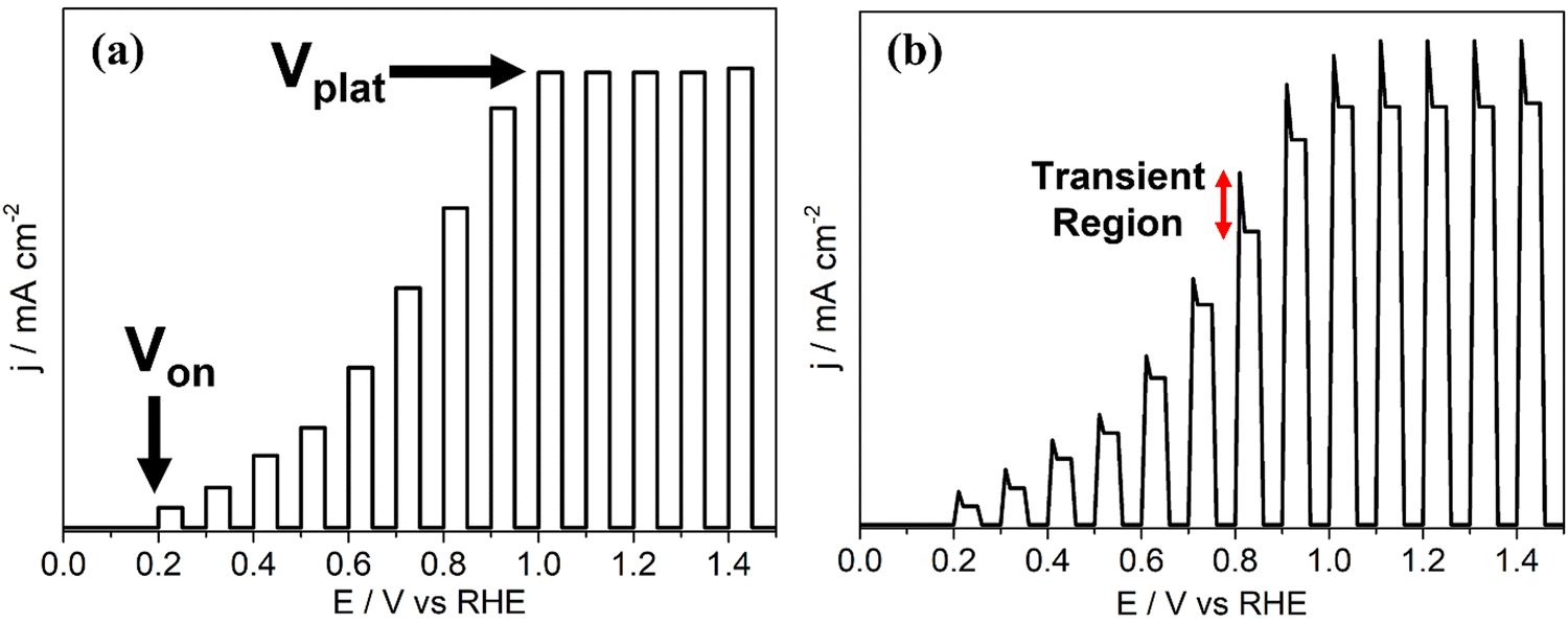 | ||
| Fig. 6 Photocurrent density (j–V) graphs for example systems under chopped light showing (a) onset potential, Von, and plateau potential, Vplat, (b) photocurrent transients. | ||
Often, the intrinsic electric field from the space charge region is not sufficient to support carrier transport and interfacial charge transfer rates high enough for catalysis to occur before recombination. An external potential bias is applied to enhance both properties and support facile catalysis at the electrode surface. The onset potential (Von), seen in a photocurrent density voltammogram as a current onset (Fig. 6a), is the minimum bias required to prevent generated charge carriers from complete recombination before surface catalysis, or other detrimental processes such as self-oxidation, occur.36 In a tandem PEC system, the potentials at which HER and OER occur can overlap, in which instance Von is the bias at which the photoanodic current (from OER) is equal in magnitude to the photocathodic current (from HER). In practice, Von is a combination of the energy required for sufficient charge separation and interfacial transfer, and the intrinsic overpotential of the half reaction taking place at the electrode surface. After Von, further increasing the bias improves electron–hole lifetimes and accelerates the rate of interfacial charge transfer, yielding greater photocurrents until the device is operating at maximum energetic efficiency and the current plateaus (Vplat, Fig. 6a). After reaching Vplat, jphoto is limited by carrier generation and/or the availability of the target species reaching active sites (i.e. mass transport in the electrolyte), and not charge carrier separation or surface electrocatalysis.
In practice, jphoto–Vbias voltammograms will have anodic and cathodic transients, observed as ‘spikes’ at each photocurrent onset corresponding to the light source being chopped on, as indicated in Fig. 6b. An anodic transient on a photoanode results from photogenerated holes becoming trapped in deep electronic energy levels due to the existence of detrimental surface states at the electrode–electrolyte interface, and/or defects in the bulk. Trapping of photogenerated carriers (in this case, holes) prevents recombination and hence allows a transient current to flow until all surface states are filled, after which charge recombination resumes as expected. When the illumination is stopped, these surface-trapped holes are discharged and reduced, resulting in a cathodic transient.48 Larger transients are therefore an indication of the presence of a greater number of surface states (minimised by surface passivation and/or electrocatalyst loading, Section 4.2), and/or the presence of deep electronic traps in the bulk due to defect formation, either by design or intrinsically. In the latter case, these transients show the potential photocurrents that could be achieved if the traps were shallow instead of deep (i.e. charge carriers could be promoted and relaxed rapidly through them). Hence, observation of such phenomena using chopped light provides identification of the depth of traps produced, as discussed in Section 4.3.49–51
Faradaic efficiency (FE). FE is a useful tool for identifying whether measured photocurrent is due to desired water splitting, or side reactions and/or photocorrosion. FE is expressed in eqn (6):
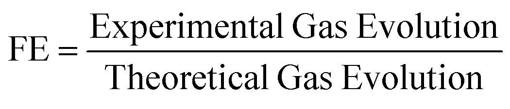 | (6) |
Incident photon to current conversion efficiency (IPCE). IPCE is a measure of the total photocurrent generated per unit incident photon flux as a function of the incident photon wavelength.25,52 It provides an invaluable insight into how the material functions, combining efficiencies from photon absorption, charge transport from excitation point to electrode–electrolyte interface, and the efficiency of interfacial transfer. The main limitation of IPCE is that it requires the assumption of 100% FE, where all electrons measured as current are used in the water splitting reaction, with no losses to side-reactions or photocorrosion.47 IPCE is expressed in eqn (7):
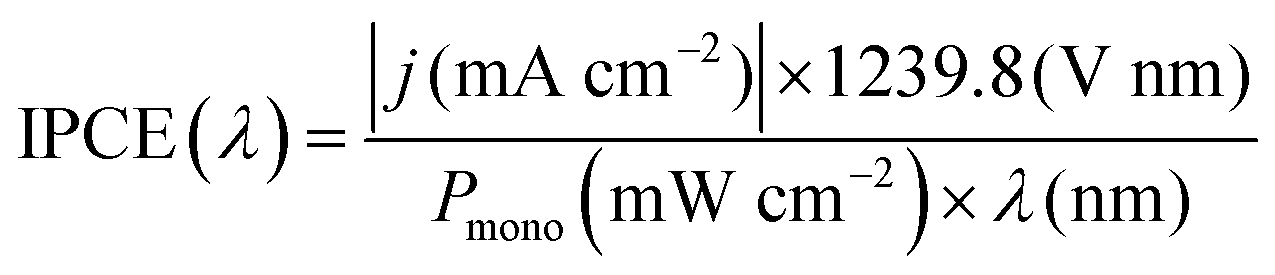 | (7) |
Solar to hydrogen conversion efficiency (STH). STH provides the ‘truest’ efficiency representation of the material, as it defines the efficiency with no applied bias potential and only when exposed to broadband AM 1.5G solar simulation (100 mW cm−2); calculated as in eqn (8):
 | (8) |
Photostability is typically measured via chronoamperometry of the photoanode while under constant illumination for prolonged periods. The measurement is usually run for 24–72 hours at lab scale, however, for more technologically ready electrodes that are targeting commercialisation, durations can be as long as 5000 hours.47 These tests should be repeated at multiple biases, chosen as those that provide photocurrents expected within commercial PEC operation (1–10 mA cm−2),47 and re-characterisation of the electrode, both physically and photoelectrochemically, should be performed after each stability test.
3. Photoelectrode materials
There is an abundance of text already published that give in depth discussion of various materials for photoelectrodes,4,57–61 hence only a brief outline of the most common and promising materials will be given here. A list of the materials discussed in this section, including their key properties, advantages, and limitations, is given in Table 1.| Material | Photoelectrode | E g/eV | Key advantages | Key limitations |
|---|---|---|---|---|
| TiO2 | Photoanode | 3.0–3.2 | High stability, low cost, non-toxic, moderate carrier diffusion length | Large bandgap |
| α-Fe2O3 | Photoanode | 2.0–2.2 | High stability, low cost, non-toxic, good bandgap | Short carrier diffusion length |
| Fe2TiO5 | Photoanode | 2.2 | High stability, non-toxic, good bandgap, moderate carrier diffusion length | High temperature synthesis, often impure films |
| BiVO4 | Photoanode | 2.4 | High stability, non-toxic, good bandgap | High surface recombination, poor bulk carrier transport, requires pH control |
| WO3 | Photoanode | 2.5 | High stability (acidic pH), non-toxic, moderate bandgap | Poor surface/interfacial carrier transfer, poor stability in non-acidic pH |
| Cu2O | Photoanode | 2.0–2.1 | Low cost, non-toxic, good bandgap | Poor photostability |
| SnS | Photocathode | 1.1–1.3 | Good bandgap, low cost, high carrier mobility | Secondary phases act as deep hole traps, poor stability |
| CdS | Photocathode | 2.4 | Good bandgap, low cost, high catalytic activity, | Toxic, poor photostability, rapid carrier recombination |
| ZnS | Photocathode | 3.7 | Good stability, low cost, non-toxic, good catalytic activity | Very large bandgap |
| Sb2Se3 | Photocathode | 1.2 | Good bandgap, high bulk carrier mobility | Poor stability |
3.1 Photoanodes
Photoanodes are typically made from n-type metal oxide materials due to the positive position of the VB above the O2/H2O redox reaction potential, and the intrinsically high stability towards electrode oxidation. Here, the properties of four of the most common metal oxide photoanodes will be summarised.Research has proven the ability to control the dimensionality of the TiO2 nanostructure, with published syntheses for zero-dimensional (0D), one-dimensional (1D), two-dimensional (2D), and three-dimensional (3D) nanostructures. Of these, 0D and 1D are the more useful for application in PEC water splitting. 0D usually takes the form of quantum dots, used to decorate a photocatalyst and improve light absorption and carrier separation.67 1D usually takes the form of nanorods or nanotubes which feature high surface areas for redox catalysis to occur on as well as small distances for photoexcited carriers to reach the electrode–electrolyte interface.68,69 The choice between nanotubes and nanorods will depend on the kinetics of the charge transport in the semiconductor and the efficiency of redox catalysis at the surface. If the device activity is limited by the number of carriers available for catalysis at the surface, then nanorods are the more effective morphology as there is more material for light absorption and hence more charge carrier generation. On the other hand, if the limitation is the rate at which reactants in the electrolyte can reach the active sites on the electrode, nanotubes are more effective as they have a far greater surface area with a greater number of available active sites.70,71
The main focus of TiO2 research has been in two main areas, (1) tuning its large band gap (∼3.2 eV, 387 nm), which limits its light absorption to the near-UV/UV regions of incident light, just 3.3–5.0% of all incident radiation,21,37 (2) slowing down the rate of recombination of photogenerated electrons and holes to improve quantum efficiency.72 Promising methods to enhance these properties in TiO2 devices include annealing, nanostructuring, electrocatalyst loading, cation and anion doping, and heterojunction formation.43,73
Crystalline TiO2 can exist in three phases, anatase, rutile, and brookite; crystalline structures for these polymorphs can be seen in Fig. 7. Rutile is the thermodynamically favoured structure and can be achieved directly in deposition or by heating the metastable anatase or brookite states at temperatures exceeding 600 °C.74 All three phases are semiconducting, have band edges positioned suitably for both OER and HER, and have band gaps of 3.2 eV, 3.0 eV, and 3.2 eV for anatase, rutile and brookite, respectively. It is generally accepted that neither brookite nor amorphous-TiO2 (a-TiO2) are promising candidates for photocatalysis, and hence the discussions herein will focus on either anatase or rutile.44 It is worth noting that anatase is considered the more photochemically active form of TiO2, despite its greater bandgap than rutile.75
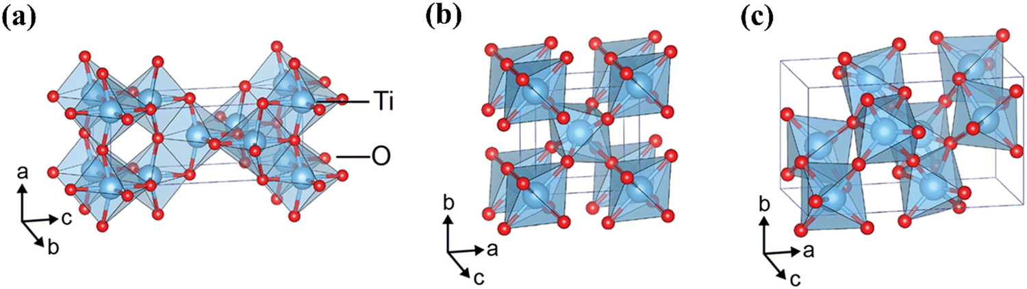 | ||
| Fig. 7 Crystalline structures of TiO2 in polymorphs (a) anatase, (b) rutile, (c) brookite. Reproduced with permission from ref. 76 copyright 2017, Nature Portfolio. | ||
Pure TiO2 is an n-type semiconductor because of intrinsic oxygen vacancies, which effectively serve as electron donor sites to reduce some of the Ti(IV) centres in the lattice to Ti(III) (Fig. 8). Such a reduction has been increased extrinsically by a range of techniques, including high pressure hydrogen treatment,77 reduction using aluminium reducing agent,78 and annealing under vacuum environment.13 Acceptor doping (e.g. Cr3+, Fe3+)79,80 into TiO2 can modify it into a p-type semiconductor for use as a photocathode. Naturally, this also adds additional dopant energy levels above the VB which serves to narrow the band gap (to absorb a wider photon range from the visible light spectrum) and improve the rate of charge transport inside the semiconductor.81 Indeed, lowering the bandgap by doping, with either acceptor or donor dopants, has proven highly successful for the viability of TiO2 in commercial photocatalysis, however, the most effective dopants are often noble metal ions which are too expensive and rare for large scale, sustainable production.44 A promising alternative to noble metal usage is in sulfur-doped TiO2, or similarly the combination of TiO2 with metal sulfides, such as MoS2 and WS2, both options producing much cheaper, more abundant semiconductor devices with photochemical properties comparable to those using noble metal ions.82,83
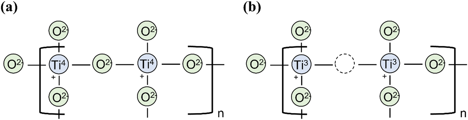 | ||
| Fig. 8 (a) Defect free rutile TiO2. (b) Intrinsic oxygen vacancy in rutile TiO2 causing reduction of Ti4+ to Ti3+ in the lattice to conserve overall charge neutrality. | ||
A promising hybrid material using both α-Fe2O3 and TiO2 is Fe2TiO5 (iron titanate), retaining the advantages of each material, while also improving upon the limiting properties of each, such as the large band gap of TiO2 (Fe2TiO5 has a much narrower bandgap of around 2.0–2.2 eV) and the poor charge carrier conductivity and diffusion lengths of α-Fe2O3.86,87 In addition, the CB and VB positions of Fe2TiO5 are ideally placed to facilitate both HER and OER (Fig. 9).88 Iron titanates are formed via solid state reactions between TiO2 and α-Fe2O3, however, due to the similar metal ion sizes, films can be created by simultaneous, dual deposition of Ti and Fe oxides followed by thermal annealing, where the properties and structure are controlled by the relative concentrations of Fe and Ti ions.88,89 The requirement for high temperature annealing can result in Fe2TiO5 films containing Fe and Ti oxide impurities.
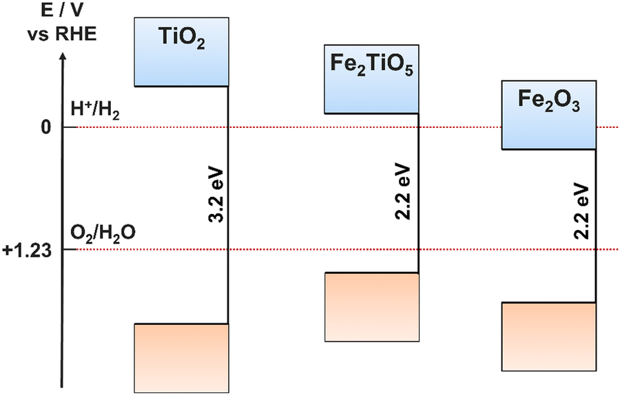 | ||
| Fig. 9 Band positions for TiO2, α-Fe2O3, and Fe2TiO5. | ||
There are limitations to the viability of BiVO4 photocatalysts, the first is that it cannot be run on its own in photocatalytic systems, or even for OER PEC catalysis at low potentials due to high surface recombination resulting in low IPCE values at lower biases.91 The VO4 octahedra that make up the BiVO4 lattice result in poor carrier mobility, forcing hopping between octahedra instead of a constant motion through the lattice. Doping with W or Mo metals is considered essential in BiVO4 to overcome this, substituting into the V sites, and distorting the octahedra to promote easier movement through the lattice.92 BiVO4 can also have a poor photocurrent stability due to the dissolution of V5+ on the surface, and the build-up of oxidation products at the anode surface which act as recombination centres. Decreases in photocurrent densities of up to 75% have been reported after just 30 minutes, highlighting the need to modify such electrodes or coat with protective layers.93
3.2 Photocathodes
Photocathodes are a significant bottleneck in the development of an overall PEC device. The intrinsic electric field originating from the space charge region in p-type semiconductors make them suitable for proton reduction/hydrogen evolution, however, stability and photocorrosion is a ubiquitous issue across the range of potential candidates. It is well understood that PEC cells combining a photoanode with a complementary photocathode will lead to the highest theoretical efficiency, hence it is an issue that must be solved.99 There is therefore great interest in both emerging photocathode materials that show good stability while still performing effectively, and in electrocatalysts and protective layers that can be coated onto the unstable materials to make them viable.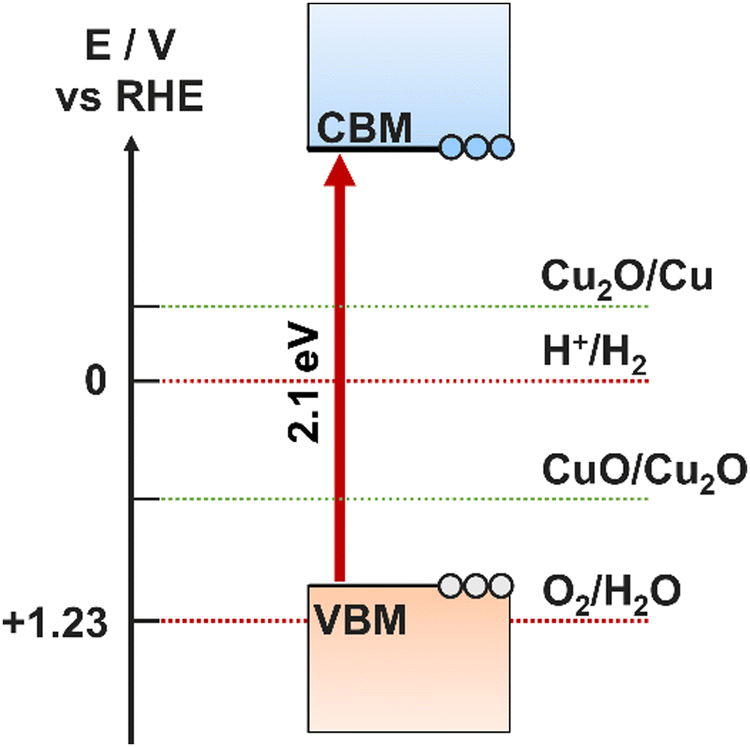 | ||
| Fig. 10 Positions of CB and VB relative to self-oxidation and self-reduction potentials for a Cu2O photocathode. | ||
Research on the optimisation of Cu2O photoelectrodes has revealed multiple methods by which the extent of photocorrosion can be suppressed. The most common method, but also the method with the most breadth in variables to optimise, is to coat the electrode with a protective layer, often a hydrogen evolution catalyst such as MoSx.105 This has the added benefit of improving the surface charge transfer and reducing bulk recombination, as well as increasing stability. TiO2 is another protective choice that has suitable band positions for p–n heterojunction formation, however, it requires complete coverage and good charge transfer, and therefore it is often used with another semiconductor to form a bi-layer coating the Cu2O.106,107 This method also requires the deposition of reduction cocatalysts to ensure the effectiveness of proton reduction is not lost in place of increased stability.100
CdS is generally considered a good photocatalyst material for PEC water splitting, possessing a bandgap of 2.4 eV with a suitably positioned CB for HER and VB for OER, and high catalytic activity, however, environmental concerns and rapid carrier recombination have limited its use.116,117 It is often coupled with more stable materials such as ZnS, TiO2, WO3, and amorphous carbon to counteract its high photocorrosion, as well as form heterojunctions to minimise its intrinsically high recombination rates.118,119 ZnS is like TiO2 in that it is nontoxic, earth abundant, and shows good catalytic properties with suitable band edge positions for both OER and HER. However, its 3.70 eV bandgap is even greater than that of TiO2, making it unsuitable for use without band structure engineering, for example, by doping, and combining/layering with lower band gap materials.120
Many reports have been looking at chalcogenide materials already extensively studied for use in PV systems and repurposing them for PEC photocathodes, including Sb2Se3, Cu2BaSnS4 (CBTS), Cu2ZnSnS4 (CZTS), and CuS2. Due to the nature of PV requirements, all promising options have small bandgaps with CBM and VBM positioning only suitable for photocathodic use. The existing, well studied, and optimised multi-component PV devices based on these materials gives a good starting point for PEC photocathode development, often only requiring slight modifications with electrocatalyst or stability coatings.4
Sb2Se3 is an emerging material for use as a photocathode in PEC water splitting, with a small bandgap of ∼1.2 eV facilitating absorption into the near-IR region, and good bulk carrier mobility.121 It was first reported for PEC application in 2017, where it was used with n-type TiO2 and Pt co-catalysts.122 It can be seen from the use of anti-photocorrosion layers in most reports that stability is still an issue, however, after TiO2-based protective layering, along with loading a Pt or RuOx cocatalyst to ensure efficient HER catalysis can occur, water splitting performances are promising and stability is no longer an issue – unlike the Cu-based photocathodes which still show instability even after a protective coating.123,124 A 2018 study by Malik et al. synthesised Sb2Se3 nanorods by both hot injection and aerosol-assisted chemical vapour deposition (AACVD) techniques using a novel single-source precursor (SSP), which showed high stability under simulated sunlight illumination for 10 minutes, longer than most Cu-based and chalcogenide photocathodes are stable for, however, longer durations would be required to assess long-term stability, and for comparison to photocathodes with protective layers.125
CBTS, CZTS, and binary sulfides such as CuS2 are earth-abundant PV materials that have been investigated for photocathode application. Again, after slight modification from their use in PV, for example, Se incorporation into CBTS,126 and deposition of buffer layers and TiO2 protective overlayers,127 current performances seem promising, although to date not competitive. Promisingly, the significant gap between current PEC performance and PV performance indicates that there is still lots of potential for performance enhancement within these materials.128
4. Design of important photoelectrode properties
Regardless of the electrode material, there are a range of important properties that need to be considered, improved, and implemented to create a highly efficient photoelectrode. To effectively design a precursor, it is essential to understand these properties that should be targeted for improvement. Literature case studies outlining how precursors can be designed to control the properties discussed herein can be found throughout Section 5.4.1 Charge carrier transport within the bulk
The first challenge faced by photogenerated charge carriers is successful transport through the bulk material to the relevant interface, usually either the semiconductor/electrolyte or semiconductor/back-contact interface, before recombination occurs. It is therefore crucial to study and control the bulk charge carrier mobility through a range of photoelectrode design techniques, as outlined herein. Doping and heterojunction formation are both effective and well-used approaches towards improving bulk transport, however, due to their versatile application towards engineering a range of different electrode material properties other than this, they are instead discussed in greater detail in Sections 4.3 and 6.1, respectively.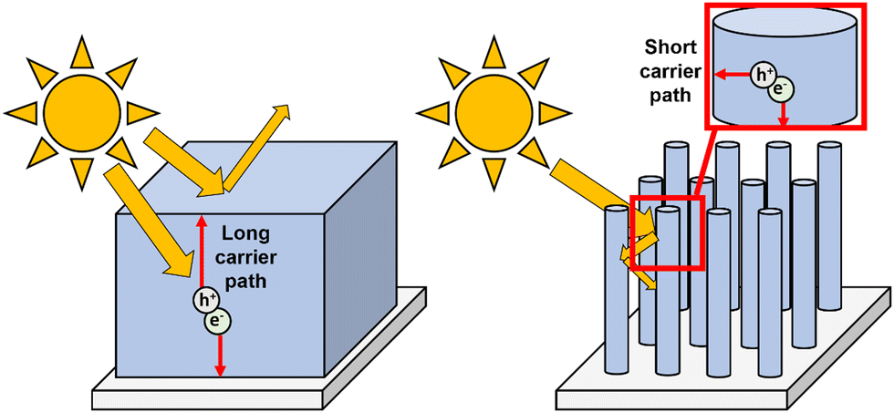 | ||
| Fig. 11 Schematic comparisons of light trapping and carrier diffusion distances in a flat film versus nanorods. | ||
In TiO2, exposed (101) and (010) facets are usually considered as the most photoactive, due to the increased number of uncoordinated atoms at the surface,137,138 or the abundance of 100% coordinated Ti5c atoms at the surface which can more efficiently transfer charge carriers, reducing recombination.139 While certain precursors and deposition procedures can produce films with a high abundance of desired facets directly due to the deposition and growth mechanisms, it is difficult to evaluate this before deposition trials. For a deliberate facet engineering, two techniques can be used: additive addition and templating.
Additives in the precursor solution can interact with either the precursor or the nanocrystals during growth, altering the crystallite shape and the exposed facets.140 The additives chosen must not remain after deposition, either through removal during the deposition process, or by thermal annealing post-deposition. Murray et al. was able to enhance and control the abundance of the (001) facet in TiO2 nanocrystals using TiF4 precursor with oleic acid and cosurfactant additives to produce HF in situ, which selectively binds to the (001) facet, preventing termination and maintaining exposure during continuing crystal growth.138 With the use of different cosurfactants and the introduction of a percentage of TiCl4 instead of TiF4, the amount of facet exposure could be controlled, as well as the resulting overall crystal morphology.
Templating is another common method for controlling the shape of nanostructure during deposition,141,142 however, it can also be used to selectively grow specific crystal facets. Zhou et al. demonstrated the use of a salt template to grow specific planes of transition metal phosphines (TMPs) due to the lattice matching between the salt crystals exposed facets and the grown TMP planes.143,144 Theoretically, any preferred material orientation can be grown provided a suitable template with lattice matching exposed planes, however, it may limit other morphological requirements such as shape and surface area. Templating and additives also add additional material costs and fabrication steps to photoelectrode synthesis, hence achieving similar effects through bespoke precursor design would be advantageous for scale-up application.
Carrier mobility between grains is correlated to how intimately connected neighbouring grains are, hence a sample with a larger range of different grain sizes can often form stronger connections and therefore show greater transport properties; however, this can also increase the density of grains, introducing more energy barriers to move through and also increasing charge mobility degradation rates due to greater diffusion of ambient species into the film, which can then act as energy traps.147–149 Mixed phase films, like anatase–rutile TiO2, will likely contain different sized grains due to the differing growth rates and mechanism of each phase, hence often showing increased bulk charge mobility due to the resulting formation of more intimate contacts.150 Grain sizes can be controlled by the decomposition rate of the precursor molecules, but also by deposition (see Section 5.1.3) and annealing conditions.
4.2 Charge carrier transfer at surfaces
Surface charge utilization is as important as bulk charge behaviour, as poor interfacial transfer will result in significant efficiency losses through carrier recombination.The porosity is also important to consider. While a more porous material will have a greater surface area and thus higher efficiency, it is important to note that a performance decrease with time for materials with extreme porosity may be seen, as solution ions around active sites are consumed but cannot be replenished due to the difficulty of transport through the pores (i.e., mass transport limitations). Nanostructures such as nanorods/nanotubes are among the most promising due to their high surface area, as well as ordered perpendicular growth relative to the substrate surface allowing for easy transport between the solution bulk and the base of the pores.151 Ordered growth can also allow for more control over active areas of the crystal, increasing the exposure of specific facets.
There are four photoanode properties that can be improved using passivating layers: (i) increased stability, preventing photocorrosion by increasing the speed of charge transport and removal from the electrode material to the passivating layer or solution. Chemical dissolution from instability of the electrode material in aqueous solution can also be eliminated by coating with a protective layer of highly chemically stable semiconductor, common examples being TiO2 and WO3.53 (ii) Minimised surface state charge trapping, and therefore recombination, due to non-empty surface states acting as photogenerated hole traps. This phenomenon is caused by defects, dopants, and vacancies at the surface, hence deposition of a passivating layer eliminates charge traps at the electrode–electrolyte interface.152,153 Use of a passivating layer also prevents the need for high temperature annealing to remove these states, which is known to negatively alter morphologies and material phases/polymorphs.154 (iii) Decreased charge accumulation at the back contact, usually caused by poor band alignments between the photoanode and the back contact.155 A thin passivating layer with a very negative VB at this interface also blocks hole backflow, a phenomenon where both holes and electrons are injected into the highly conductive back contact, so recombination can readily occur.156 (iv) Manipulated interfacial energies; layering semiconductors with suitable bandgaps can lead to improved charge transfer throughout the device due to band bending facilitating more favoured transfers of carriers between materials.42,157–159
Alternatively (or in addition) to passivating layers, co-catalyst loading is a common method for enhancing surface charge utilization. OER and HER kinetics are improved by surface-bound electrocatalysts through reduction of the interfacial charge injection overpotential. The highest performing electrocatalysts are noble metals (Pt,160,161 Pd,162 Ru,163,164 Rh,165 Au,166 Ag167) and noble metal oxides (RuO2,168,169 IrO2170), however, due to their high costs and rarity, extensive research is aimed at finding alternatives to facilitate more viable commercialisation and scale-up, including materials such as transition metal phosphides171–173 and oxyhydroxides.174,175 Complex, multicomponent catalysts are emerging as highly efficient multi-functional systems, where the range of species present facilitates use in both HER and OER, a particularly useful trait for PC devices.176
There is a wide range of techniques used for co-catalyst deposition, including electrodeposition,173,177 photodeposition,178 ALD,56 hydrothermal,83 and precipitation.172 Co-catalysts with complementary band structure to the photoanode can also enhance charge carrier transport and separation throughout the device in the same way as discussed for passivating layers, acting as a heterojunction, and if the electrocatalyst is coated across the entire surface, or by photodeposition to cover the photoactive sites, stability can also be increased.87 A rudimentary test for the photocurrent difference with and without an electrocatalyst can be achieved by running a linear sweep voltammetry measurement under chopped illumination before and after addition of a hole quencher (e.g. H2O2) into the electrolyte (Fig. 12). The difference in measured photocurrent can be correlated to the photocurrent loss due to poor surface charge transfer kinetics.179
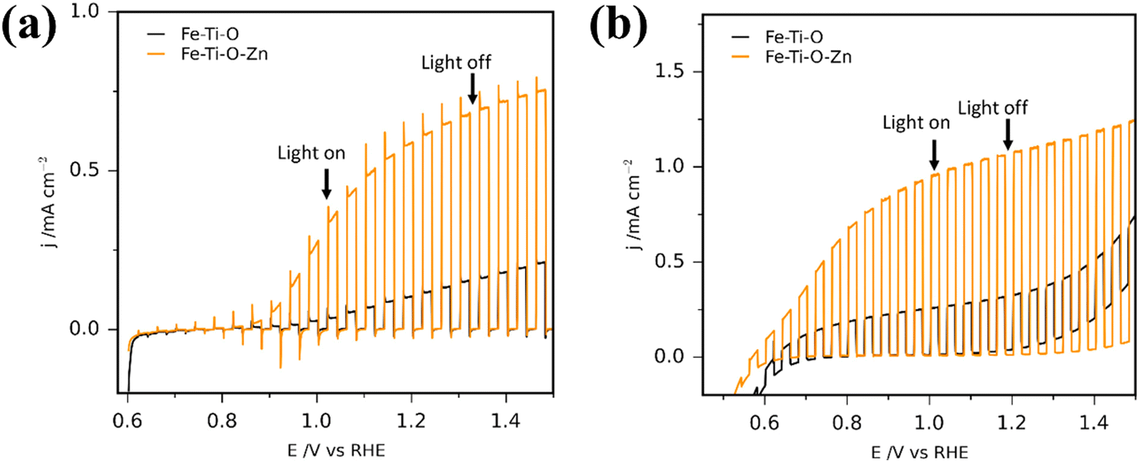 | ||
| Fig. 12 Photocurrent density plots for Fe2TiO5 and Zn-doped Fe2TiO5 photoanodes (a) without hole quencher present, (b) with 10% H2O2 in the solution. Reproduced with permission from ref. 179 copyright 2020, American Chemical Society. | ||
4.3 Point defects – dopants and vacancies
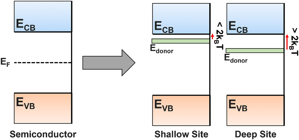
The introduction of dopants into a semiconductor is one of the most powerful tools for improving and controlling the properties of a film. The substitution of an anion or cation dopant into the lattice can have a variety of impacts, particularly towards the band gap and charge carrier lifetimes. It is impossible to make a real semiconductor without some level of doping due to contamination during deposition processes, or the formation of vacancies (which can be seen as a form of dopant) due to fabrication conditions or non-perfect crystal growth. Understanding their impact, and how to choose dopants, is therefore essential for PEC device development. To achieve the desired doping, molecular precursors must be designed with compatible properties for use in co-depositions, or, alternatively, effective single-source precursors must be designed and synthesised (see Section 5.3). Post-treatment, such as annealing in hydrogen or vacuum environments, can also be used to create vacancies (see Section 6.2).Dopants will narrow the bandgap through the introduction of dopant energy levels between the CB and VB of the bulk material, reducing the photon energy required for electron promotion, increasing the charge carrier density, and bringing the Fermi level closer to the valence (p-type doping) or conduction (n-type doping) band.180 These dopant energy levels can form trapping sites, but whether these are good or bad depends on the depth of the energy level (Fig. 13). A shallow trapping site (within ∼2kBT of bulk energy level) allows fast excitation into and out of the sites, still maintaining overall carrier flow but dynamically separating carriers to prevent recombination, therefore increasing the diffusion distance, but not speed. Alternatively, deep trap sites (>2kBT from the transport level) can be detrimental, permanently trapping carriers and removing potential catalytic species, while also forming a potential barrier that slows other charges due to Coulomb repulsion.145,181 It is often difficult to determine the depth of a trapping site before addition of a dopant into a previously unstudied system, so it is common to see reported a range of dopant species tested for a single film, some of which improve the performance and some of which worsen. As discussed in Section 2.3.1, deep traps are visible in j–V curves as cathodic and/or anodic transients.
 | ||
| Fig. 13 Energy level diagram for a perfect, non-doped semiconductor, and n-type semiconductors with shallow trapping sites or deep trapping sites. | ||
Dopants can also increase the bulk charge transport and conductivity of a deposit by distorting the lattice structure or generating intrinsic electric fields. Monoclinic BiVO4, for example, is well known to have poor bulk transport properties owing to its VO4 octahedra-based lattice, requiring charge carriers to make distinct, slow hops when travelling through bulk material. By doping with W, V sites in affected octahedra are replaced by W atoms, which distort the lattice geometry and allow more continuous, faster carrier diffusion.92,182,183
If the dopant species resides near to the photoelectrode–electrolyte interface, it can increase the interfacial catalytic activity. This is a good method for increasing catalytic efficiency without needing an additional catalyst loading step in the device fabrication process. Selectivity towards which species is oxidised/reduced can also change dependent on the dopant. For example, in TiO2, oxygen vacancies can be formed by reductive annealing, acting as 2-electron donors which reduce Ti4+ in the lattice to Ti3+. The Ti3+ at the surface is both more catalytically active than Ti4+, and has a selectivity towards chloride oxidation over hydroxide, as shown in work by Marken et al. where TiO2 in a solution of KCl was inactive to chloride oxidation before vacuum annealing, but active after.13,151
Finally, the film morphology can be altered due to the impact of dopant precursor presence on the film growth mechanisms (Fig. 14). Sathasivam et al. reported a morphological switch from an array of compact domes to a pyramidal featured thin film after doping TiO2 with W in an AACVD process, achieved by the inclusion of a W(OEt)6 precursor into the initial precursor solution.184 Parkin et al. reported a similar change upon antimony doping, again by AACVD, where the pyramidal TiO2 became a mixed pyramidal-needle morphology, increasing in the amount and prominence of the needle-like features with increasing percentage of Sb doping.185
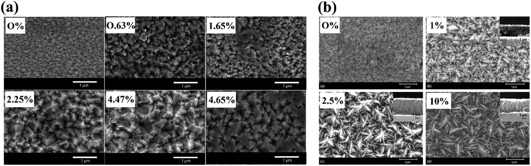 | ||
| Fig. 14 Morphological changes reported for TiO2 films after doping with varying concentrations of (a) W, reproduced with permission from ref. 184 copyright 2015, Nature Portfolio, (b) Sb, reproduced with permission from ref. 185 copyright 2017, Royal Society of Chemistry. | ||
4.4 Polymorph composition
The polymorph of a semiconductor will have considerable influence over the PEC properties it exhibits, including different band gaps, band edge positions, catalytic activities, charge mobilities, and stability. The easiest method to ensure only a single phase is present is by annealing at a temperature high enough such that all the material will be converted to the most thermodynamically favoured phase, for TiO2 for example, a temperature above 600 °C will ensure complete conversion to rutile, except in rare cases.186 To obtain a non-thermodynamically stable phase, precursor design and deposition parameters must be used to control the deposition, covered in greater detail in Section 5.5.It is possible to create a mixture of two or more polymorphs in an as-deposited material, for example, anatase and rutile phases in TiO2 films, which can modify the properties of the electrode significantly depending on the relative ratios of phases, the properties of each phase, and how compatible the phases are with each other. The possible benefits of mixed phases include: (i) the combination of best properties of each material (if one phase is better at light absorption and the other better at charge carrier transport, for example); (ii) different band gaps enhancing light absorption efficiency; (iii) aligned band positions forming an intrinsic electric field for enhanced charge separation.74,92,187 It is known that an anatase–rutile mixed phase TiO2 electrode consistently shows greater PEC performance than equivalent single-phase electrodes.150,188 Alternatively, multi-phase materials can be detrimental, particularly if one of the phases is inactive or has poor light absorption or carrier transport properties. A greater transport resistance in highly dispersed phases can also occur because of increased hopping between. Unsuitable band alignments that drive electrons and holes to the same material will also increase carrier losses through recombination.
4.5 Photostability and photocorrosion
A common occurrence on PEC electrodes is self-oxidation and self-reduction, also known as photocorrosion, a side effect of generating free charge carriers that are available to oxidise/reduce the electrode material itself in addition to targeted ions in solution.16 For self-oxidation to occur, the electrode must have an oxidation potential less positive than its VBM, and equivalently for self-reduction the reduction potential must be more positive than the CBM.189 It is therefore possible for only oxidation or reduction to occur, both, or neither on a single semiconductor. Examples for TiO2, Cu2O, and Fe2O3 are illustrated in Fig. 15, showing that all three are theoretically susceptible to oxidative photocorrosion, while Cu2O can also experience reductive photocorrosion.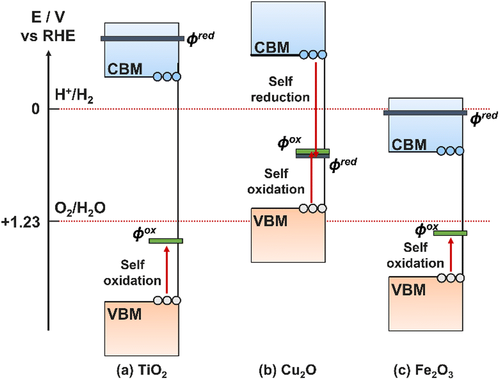 | ||
| Fig. 15 Band energy levels for three common semiconductors compared to their reduction potentials (φox, grey) and oxidation potentials (φred, green). | ||
Photocorrosion can be avoided if the reaction time for oxidation/reduction of the semiconductor is greater than the duration for complete charge carrier removal, therefore using co-catalysts is an effective approach for indirectly increasing material stability. Improved redox kinetics for the transfer of photogenerated charge carriers across the semiconductor–electrolyte interface results in faster removal of the oxidising/reducing species, therefore suppressing photocorrosion and increasing the life and activity of the device.190 Additionally, co-catalysts inhibit the back reactions of H2/O2 recombination and O2 photoreduction due to their optimised selectivity and activity. However, the most promising options are noble metals and noble metal oxides (see Section 4.2), which are not suitable for large-scale application due to their high costs, rarity, and unsustainability.191 Doping and heterojunction formation (Section 6.1) also improve charge separation efficiency, lowering the number of unconsumed charge carriers which can act towards self-oxidation or self-reduction.16
4.6 Material practicality
Even if a PEC electrode fulfils all electronic and structural requirements such that it performs perfectly, it must also be practical for application in large-scale, green, sustainable energy production and storage. The material must therefore be: (i) earth abundant; (ii) cheap to source and produce at large-scale; (iii) environmentally safe in production, operation, and disposal. Ideally, high percentage return recycling and/or regeneration of the material should be possible to minimise waste at end of life.22,24,59 Consequently, considerations must be made towards both the deposition method and precursor design beyond simply maximised performance.5. Precursor design and growth criteria for semiconductor materials
Molecular precursor design takes a systematic approach to thin film deposition, specifically engineering structures to modify the precursor thermal decomposition profile and mechanisms, increase stability and ease of handling, and open the door to a wider range of more complex precursors that can be used to deposit multinuclear, mixed phase, or uniquely structured semiconductors. This section will cover the range of options for tailoring precursor molecular structures towards both suitability for deposition, and properties of the resulting semiconducting films. Modifying the structure of a precursor to enhance a certain property will result in a change to all other properties, hence it is often necessary to work through many iterations of a precursors design, each new structure building on the benefits and limitations of the previous. A large range of case studies from previous reports of precursor design will be discussed, however, there is a distinct lack of literature on precursor design towards water splitting materials. Most discussions will therefore focus on the methods of precursor structural development and improvements towards properties for effective deposition, and resulting film properties that are required for water splitting; instead of specific examples that would report from precursor development to deposition to PEC characterisation.All molecular design features discussed in Section 5 are summarised in Table 2, along with their influence on precursor and resulting material properties. This is not an exhaustive list, but acts as a guide towards tailoring molecular precursor design for specific deposition and thin film requirements and applications. It should be noted that when designing a precursor, it is essential to consider the simplicity and cost-effectiveness of the precursor synthesis method, whether it would be suitable for scale-up and real-world applications, and how environmentally sustainable its production and use would be.192 A summary of molecular properties discussed in this section, and the measurement techniques used to study them, is also given in Table 3. It should also be noted that precursors should normally be isolated and purified at the end of synthesis to prevent contamination of the thin film, or disruption during growth, no matter what deposition technique or product is used.
| Molecular design | Precursor property | Impact on material deposition |
|---|---|---|
| Multidentate ligand | Multi-step thermal decomposition | Nanostructured material |
| Coordinative saturation for increased air/moisture stability | Easier to handle, purer material, better solubility and volatility | |
| Organic substituents sterically surrounding metal centre | Increased solubility | Faster deposition by AACVD increased solvent options |
| Increased stability | Nanostructure changes | |
| More complex decomposition | Increased carbon contamination | |
| Large organic chains on ligand | Increased solubility | Faster deposition by AACVD |
| Greater carbon contamination | Nanostructure changes | |
| Lower volatility | Increased carbon contamination | |
| More complex decomposition | ||
| Fluorinated ligand | Increased volatility | Increased decomposition temperature |
| Increased solubility | Decreased carbon/by-product contamination | |
| Increased thermal stability | Fluorine contamination | |
| Multinuclear | Require larger/more ligands | Doped and/or hybrid deposit from SSP |
| Decrease volatility | ||
| Dimer, trimer, oligomer, cluster (homo-polymetallic) | Increased thermal stability | Increased decomposition temperature |
| More complex decomposition | Unique nanostructure and/or phase materials | |
| Decreased volatility | ||
| Donor functionalised ligands | Increased air/moisture stability | Increased purity |
| Reduced oligomerisation | Access to difficult-to-make materials | |
| Increased solubility | ||
| Ligand adaptability to metal systems | Compatible metal precursors – similar solubility, volatility, thermal decomposition rates and mechanisms | High stoichiometric control in multi-source doped/hybrid materials |
| Homogeneous films | ||
| Single-step doped/hybrid material depositions | ||
| Anionic dopant species | Contain atoms that can act as dopants: Cl, F, N, C, S, Se | Single-source doped or chalcogenide materials |
| Isolated and purified precursor | High molecular purity | Increased purity |
| Consistent depositions | ||
| Building block structures | Precursor shaped for growth of desired nanostructure | Controlled growth of specific nanostructure |
| Molecular property | Measurement technique |
|---|---|
| Volatility | TGA – variation of wt% with temperature ramp |
| Isothermal TGA – volatilisation rates and sublimation enthalpies | |
| Thermal stability and decomposition kinetics and products | TGA – mechanism, decomposition rate, decomposition species and by-products (match wt% to fragment) |
| Couple with NMR, GC-MS, MI-IR | |
| Solubility | Qualitative – check transparency of solution with desired concentration of precursor in |
| Air/moisture stability | NMR before and after exposure |
| Solvent adduct formation | Single-crystal XRD |
| Molecular structure and composition | Single-crystal XRD |
| M–L bond strength | Single-crystal XRD |
In general, there are two categories of control for deposited semiconductor properties to consider: (i) the molecular precursor design; (ii) the deposition technique and conditions. When using ready-made, common precursors untailored for application such as metal nitrates, chlorides, or simple isopropoxides, ethoxides, and butoxides, not only will the precursor be unoptimized and untailored for the deposition technique and conditions, but the substantial element of semiconductor property control associated with the starting precursor will be lost, significantly limiting the potential of performance optimisation and enhancement.
5.1 Deposition requirements
The first aspect to consider when designing a precursor is the deposition technique that will be used, and the properties required for effective use in that method. Precursor deposition techniques can be split into two categories, solution-based and vapour-based. Solution-based depositions involve dissolving the precursor into a solvent solution, whereas vapour-based techniques rely on volatilisation of the precursor. It is therefore essential to consider the solubility and volatility properties of the precursor for the former and latter family of techniques, respectively.Many variations of CVD exist for different reaction activation mechanisms and precursor types, summarised in Table 4. In the simplest case, CVD involves the volatilisation of a precursor which is subsequently thermally decomposed over a heated substrate to form the target material as a thin film. The structure and behaviour of the precursor itself is therefore the most influencing factor on the fabricated thin film properties. CVD also enables great flexibility in the design of suitable precursors, including the availability for simultaneous co-depositions of multiple precursors to create more complex materials. The reader is referred to ref. 193–196 for more detailed reviews on CVD techniques.
| CVD technique | Volatility | Solubility | Advantages | Limitations |
|---|---|---|---|---|
| Low-pressure CVD | ✓ | ✗ | Simple reactor setup, good film uniformity | Higher process costs, not suitable for multi-source |
| Photo-assisted CVD | ✓ | ✗ | Lower process temperature, unique deposit structures | Higher process costs, not suitable for multi-source |
| Plasma-enhanced CVD | ✓ | ✗ | Lower process temperature, unique deposit structures | Higher process costs, not suitable for multi-source |
| Aerosol-assisted CVD | ✗ | ✓ | Precursor solubility required, multi-source suitability | Solvent decomposition contamination |
| Metal–organic CVD | ✓ | ✗ | Simple reactor setup, high throughput | Poor uniformity, low film purity compared to others |
| Atomic layer deposition | ✓ | ✗ | Highly controlled monolayer deposition | More restricted precursor requirements |
Among the techniques in the CVD family (Table 4), AACVD has a key advantage over other variations: the precursor only needs to be soluble in a solvent that can be aerosolised, without any chemical volatility requirements. AACVD is the only solution-based deposition technique in the CVD family, hence greatly increasing the range of potential precursor structures that can be used to deposit thin films, and opening the door to non-volatile, larger, and more complex precursor structures that can be used as SSPs for complex film deposition (Section 5.3), or for uniquely nanostructured films (Sections 5.4 and 5.6 respectively).197,198 The number of operational conditions that can be varied to optimise film properties is also increased with AACVD, now including choice of solvent, precursor concentration, and carrier gas flow.
Volatility of precursors is usually managed by the choice of organic groups. Ideally, the organic group of the ligand should have a large steric profile to reduce nuclearity, however, bulkier groups tend to indirectly reduce volatility by increasing the molecular weight, and increase thermal stability requiring higher process temperatures. In the development of MgAl2O4 precursors for CVD, a range of alkoxy groups have been tested and modified to achieve the best performing precursor. The molecular structure [MgAl2(OiPr)8] is a commonly used precursor, however, it was found to oligomerize during vapour transport due to the unsaturated metal centre within the framework, forming the less volatile structures [MgAl2(OiPr)8]2 and [Mg2Al3(OiPr)13].202 To prevent this, tert-butoxide (OtBu) alkoxide groups were used instead of {OiPr} to make a [MgAl2(OtBu)8] structure, with the larger ligand hopefully increasing the steric profile and hindering oligomerization. However, the bulkier {OtBu} groups also reduce volatility and increase thermal stability to decomposition, now requiring higher process temperatures than with {OiPr} groups. Expanding on this, Kim et al. replaced only the terminal alkoxide groups present on the Al atoms with methyl groups to form [MgAl2(OiPr)4Me4] and [MgAl2(OtBu)4Me4], which show greater volatility than both the [MgAl2(OR)8] compounds.203 The lower molecular weight gave better vapour-phase transport properties, however, at 600 °C, the temperature required for crystalline deposits using [MgAl2(OiPr)8], the resulting deposit for both methyl substituted precursors was amorphous, requiring annealing in air at 900 °C for crystallinity.
Veith et al. used hydride groups instead of methyl to produce the low weight precursor [MgAl2(OtBu)4H4], with higher volatility ([MgAl2(OtBu)8] vaporisation temperature = 100 °C; [MgAl2Me4(OtBu)4] 60 °C; [MgAl2H4(OtBu)4] 45 °C) and forming crystalline films at 450 °C, but now contained small percentages of residual organics.204 The choice of methyl and hydride groups in these examples was also for tailoring of decomposition products, predicting β-hydrogen elimination to form gaseous, non-contaminating methane or dihydrogen products upon decomposition (Fig. 16), as previously shown in similar ZnO and MgO precursors.205 Precursors with increasing volatility were also reported to possess increased film growth rates and surface roughness. This combination of work on MgAl2O4 precursors is a fitting example of the importance of precursor chemistry towards the fabrication process and the properties of the final material, and how minor changes to a structure can have significant influence. The focus of this small study was solely on volatility and decomposition, hence there is far more work that could be done on designing the precursor molecular structures to encompass other properties, especially targeting a film application.206
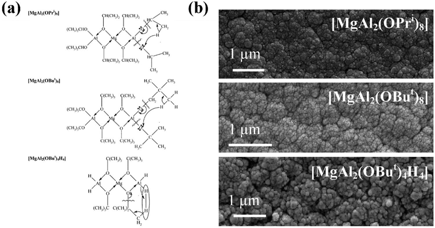 | ||
| Fig. 16 (a) Proposed decomposition methods and (b) scanning electron microscopy surface images for precursors (top to bottom) [MgAl2(OiPr)8], [MgAl2(OiPr)8], [MgAl2(OiPr)8]. Reproduced with permission from ref. 204 copyright 2004, American Chemical Society. | ||
Fluorination of alkoxide ligands is an alternative strategy reported to increase molecular volatility due to the subsequent strong repulsion between complexes from the introduction of non-bonding p electrons on fluorine, reducing intermolecular interactions.207–210 Fluoroalkoxides are also hydrophobic, providing additional stability against hydrolysis from atmospheric moisture.207 While fluorinated ligands are sometimes reported in SSPs for fluorine-doped materials,211 most commonly fluorine-doped tin oxide (FTO),212,213 it is feasible to fabricate thin films without fluorine incorporation despite using fluorinated precursors. The strong C–F bond means complexes will thermally decompose into more stable fluorine-containing fragments, removing the fluorine atoms as process-inert by-products and preventing incorporation into the film.214 Of course, the greater the temperature of the deposition process, and more reactive the precursors and thermal by-products, the greater the likelihood of fluorine contamination. For a more in-depth discussion of fluorinated ligands used in inorganic material precursors, the reader is directed towards the review by Mishra and Daniele.215
The solubility of the precursor can be indirectly improved using perfluorinated alkyl chains and CF3 groups, which are less π-donating than the conventional organic equivalents, therefore favouring low-nuclear (monomeric and dimeric) structures and suppressing aggregation, leading to greater solubility.215 Additionally, the strong secondary M–F bonds that are formed with oxophilic metals increases the metal coordination number to prevent the formation of multinuclear complexes and maintain high solubility. These secondary bonds also increase the thermal stability of the complex,209 which would normally be considered a negative result of fluorination, however, it does provide a means to control and tune decomposition temperature without significantly changing the overall molecular structure that has been designed. This is particularly useful when designing a precursor to be compatible with an already existing process, or for co-depositions of two or more different precursors, all requiring similar decomposition temperatures and kinetics to ensure a homogeneous film deposition across the substrate.
Organic solvents are often required due to the air and water instability of many molecular precursors; hence precursors should be designed with organic chains or groups to increase solubility in these solvents. There is a balance between larger organic moieties which maximise solubility, and smaller groups which facilitate lower energy and cleaner thermal decomposition.218 The polarity of the molecule will also determine which solvents the precursor is soluble in ref. 216 and 219. Solvents containing potential contaminants such as fluorine and chlorine should be avoided.
Carbon contamination in processes near or above the thermal decomposition temperature of the solvent is inevitable. Interestingly, the carbon particles from this decomposition can act as nucleation sites during film growth, influencing film properties including crystal orientation, nanostructure, grain size, and phase.220,221 The carbon contaminants can be easily removed by annealing post-deposition, but the impact on the film morphology and growth will remain. The selection of solvent must therefore include considerations towards thermal decomposition temperatures compared to the process temperature being used, and if the result of carbon contamination on the final film nanostructure and grain size is beneficial or detrimental.
Many complexes will form adducts with the solvent molecules they are dissolved in, altering the structural and thermal properties. For particularly reactive precursors, this can bring the advantage of increased air/moisture stability due to steric saturation of the metal centre.222 Some solvent adducts will impact the thermal properties more significantly than others, partially dependent on how easy the solvent is to remove upon heating, and hence how much the decomposition/volatilisation of the precursor is altered. Buchanan et al. compared diglyme, tetrahydrofuran (THF), and dimethoxyethane (DME) solvent adducts to solvent-free species for metal–organic chemical vapour deposition (MOCVD) precursors (targeting volatility) and found that the introduction of solvent adducts, particularly DME, not only increased the stability of the precursors due to steric saturation of the metal centre, but also the volatility.214 The bidentate nature and low boiling point of DME contributed to it performing best in both aspects, increasing steric saturation while still being easily removed upon heating.
In AACVD, the volatility and viscosity of the solvent also has significant impact on the deposition. Degradation of more volatile solvents usually occurs sooner and faster upon entering the heated furnace, leading to the formation of more particulates compared to less volatile solvents. These act as nucleation sites, inhibiting crystallite growth when in excess and therefore yielding smaller crystallite sizes.221 Eslava et al. demonstrated this with a titanium oxo/alkoxy cluster TiO2 precursor, deposited using either toluene or THF solvents, identified as the only suitable solvents with good precursor solubility.139 As expected, THF, the far more volatile solvent, resulted in smaller grain sizes and smaller overall plate-like sheets in the nanostructure, yielding photoanodes with lower PEC performance, suggested to be a result of a decrease in the exposure of the most active TiO2 (010) facets. Interestingly, the lower viscosity of THF compared to toluene (0.55 vs. 0.59 cP at 298 K)223 should lead to superior grain growth due to the more consistent aerosol generation and increased spray volume rate providing an uninterrupted, stable supply of precursor.224,225 Larger, well-connected grains promote greater electronic conductivity by reducing grain boundary areas, and the number of grain interfaces charge carriers must travel across.226,227 As shown by Eslava et al., this does come with the side-effect of significantly higher precursor usage rates for lower viscosity solvents (0.3 and 0.7 ml min−1 for toluene and THF respectively), which could be useful if the increased usage correlates to increased film growth rate/thickness, however, in this instance the films had similar thicknesses after the same duration, and thus the increased usage corresponds to wasted precursor and solvent.
The choice of solvent can determine both the structure and phase of the deposited films. Parkin et al. reported the AACVD of TiO2 onto steel substrates using methanol, ethanol, hexane, dichloromethane (DCM), and isopropanol solvents.217 Methanol yielded exclusively rutile phase films, while all other solvents exclusively anatase. Interestingly, when mixing methanol and ethanol solvents, the phase became majority rutile at just 10% methanol, and was exclusively rutile at ≥50% methanol, implying methanol solvent had a stronger impact on the deposition mechanism. The morphology of the films also varied with varying mixtures of ethanol and methanol, ranging from plate-like crystallites in 100% ethanol, needles in 100% methanol, and block-like crystallites in mixtures (Fig. 17). Methanol solvent has been previously reported to act as a reducing or oxidizing agent due to its thermal breakdown mechanism forming carbon dioxide and hydrogen, an explanation for this variation from ethanol deposits despite the similar solvent properties.228 Carmalt et al. used hexane or DCM in an in situ AACVD reaction for NbS2 and TaS2 films, which showed significantly different sized cluster morphologies depending on the solvent, however, the larger, and less uniform, clusters were grown using hexane for TaS2 but DCM for NbS2.229
 | ||
| Fig. 17 Scanning electron micrographs of TiO2 grown on steel substrate by AACVD use carrier solvent of (a) ethanol, (b) methanol, (c) 10% methanol and 90% ethanol, (d) 25% methanol and 75% ethanol. Reproduced with permission from ref. 217 copyright 2012, Wiley-VCH. | ||
The use of solvents for precursor synthesis in situ can produce films with higher purity and reduced oxygen deficiency,230,231 while also eliminating the need for precursor purification and isolation, increasing the efficiency of both production time and cost. Additionally, it provides an alternative means of deposition for precursors that are difficult to isolate, and different morphologies can be constructed dependent on the solvent reactant used.232 Carmalt et al. studied in situ precursor synthesis in CVD applications in detail, first fabricating In2O3 films from the AACVD reaction of Me3In and ROH,233 then reporting the first use of AACVD for Ga2O3 fabrication using [Ga(NMe2)3]2 and ROH,231 and comparing the use of 2 pre-made diorganoalkoxygallanes in low pressure CVD (LPCVD) with in situ equivalents made from Et3Ga and excess ROH in AACVD (Fig. 18).230 LPCVD resulted in oxygen deficient Ga2O3 thin films, whereas the in situ synthesis of precursor in AACVD gave stoichiometric Ga2O3. This was suggested to be a result of low oxygen content in the precursor molecule, but excess alcohol in the in situ reaction increased oxygen availability in the deposition chamber and prevented deficiency. The precursor synthesis reaction must be studied and optimised before use in deposition to ensure a full understanding of the chemicals present in the reaction chamber. More reactive input species are preferred to guarantee a complete reaction before entering the chamber.
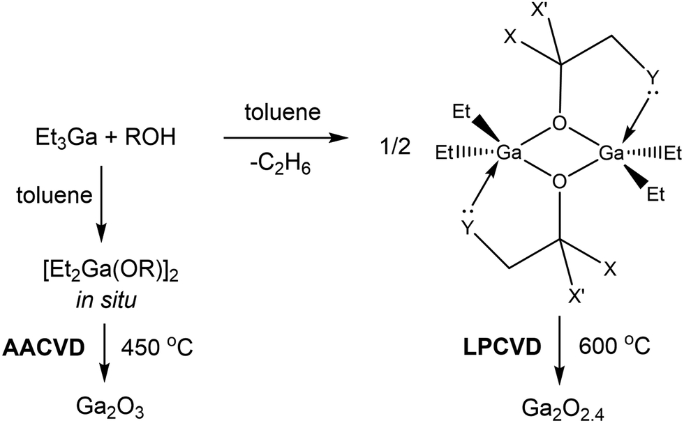 | ||
| Fig. 18 In situ precursor formation, using AACVD and lower process temperature, versus pre-deposition synthesis, isolation, and purification; R = CH2CH2NMe2, CH(CH3)CH2NMe2, C(CH3)2CH2OMe, or CH(CH2NMe2)2, X and/or X′ = H, CH3, or CH2NMe2; Y = NMe2 or OMe.230 | ||
5.2 Ligand structure
While solubility and volatility only need to be considered for solution or vapour-based deposition techniques respectively, all precursor properties discussed herein can be applied for all deposition methods and target photoelectrode materials. Section 5.2 will cover the fundamental aspects of ligand design for any new precursor ranging from small, simple structures to large, complex structures.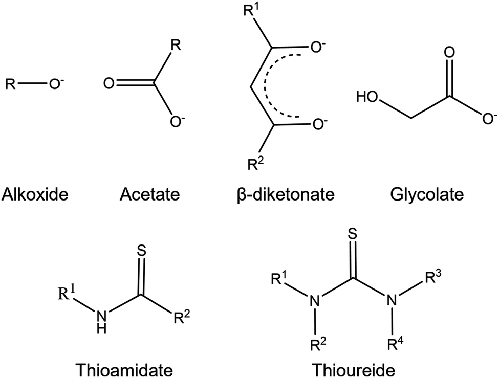 | ||
| Fig. 19 Common ligands used for metal oxide and metal sulfide precursors. | ||
The high reactivity of alkoxides makes them sensitive to moisture exposure, forming clusters or metal oxide particles due to partial hydrolysis which cannot deposit in the same way as the precursors, or at all. This decreases the ease of handling and use, requiring inert conditions during synthesis and deposition.219 Fortunately, the molecular design can be altered to increase stability without losing the beneficial alkoxide properties. Larger, multinuclear complexes with oxo-bridges and alkoxide ligands (metal oxoalkoxides) can be synthesised by the non-hydrolytic condensation of alkoxides, usually showing higher solubility, lower volatility, and greater thermal and chemical stability.200 Alternatively, multidentate alkoxide ligands can be used to reduce the number of terminal, hydrolysable alkoxide groups and provide greater steric protection around the metal centre, increasing the chemical stability without significantly increasing the molecular size or number of metal atoms.207,240
While most precursor design case studies in this review focus on metal oxide precursors, it is important to note that the same understanding can be applied to the growing field of metal chalcogenide precursors. It is most common to use dual-source precursors to deposit a metal chalcogenide, usually a precisely designed metal alkyl coupled with H2S, however, it is becoming more apparent the advantages of SSPs for the development of these materials. Thiolate ligands ([R–S]−) such as thioamidates241 and thioureides242,243 (Fig. 19) are good choices for sulfur-based chalcogenide precursors due to the flexibility in the organic group structure for tailoring steric size, shape, polarity, composition, and molecular weight.244 Metal chalcogenide SSPs are discussed in detail in Section 5.3.6.
Film impurities are ubiquitous across all deposition techniques for all target materials. Carbon impurities are the most common, arising from M–C bonds that are not broken and replaced, or from thermal decomposition of carbon containing by-products. This contamination can be minimised through precursor design, using ligands that form M–O bonds (e.g. alkoxides) for metal oxide depositions, or M–N (e.g. amides) for metal nitrides. Alternatives such as M–Cl species have been reported, however, this usually then leads to chlorine contamination instead.248 In metal oxide-free materials, oxygen impurities are also a significant issue, even present if the precursor does not contain oxygen atoms due to background oxygen levels and the higher M–O thermodynamic driving forces compared to M–N or M–Cl. The simplest way to minimise this is by purging the system with extreme vacuum to make background oxygen negligible, however, this is expensive, energy intensive, and not a complete fix. Instead, the precursor can be designed to contain reducing surface conditions to prevent oxygen incorporation. Buttera et al. used a tris(dimethylamido)aluminium(III) ([Al(NMe2)3]2) precursor to eliminate carbon impurities in the PE-ALD deposition of AlN,249 yielding carbon contamination of approx. 1%; compared to trimethyl aluminium, the standard Al-based ALD precursor, which usually yields 3–6% carbon,250,251 and aluminium chloride (AlCl3) which gets similar 1% carbon impurity, but with 1–3% chlorine contamination as well.248 Despite the ultra-high vacuum used in ALD, significant oxygen contamination was present in XPS spectra, hence the precursor design was later amended to replace two dimethylamine groups with strongly reducing hydride groups ([AlH2(NMe2)]3) that can protect the metal centre from oxygen incorporation, lowering the final oxygen impurity to <2%.252
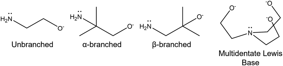 | ||
| Fig. 20 Donor functionalised ligands with no branching, α-branching, β-branching, and multidenticity. | ||
5.3 Single-source precursors
Alternatively, mixed-metal multinuclear precursors can be used to deposit complex hybrid, doped, and mixed materials as a single molecular source (Fig. 21),257 allowing deposition conditions to be tailored specifically for that single precursor, as well as introducing benefits such as higher purity of the deposited material and defining stoichiometries at a molecular level.245,258 There is, however, higher complexity in molecular composition and design, and metals within the precursor molecule must be accessible for deposition upon thermal decomposition and with the correct stoichiometries for the desired film, particularly challenging for doping where as little as a 1–5% dopant concentration is standard. SSPs will inevitably have larger and heavier structures than smaller, simpler precursors used in dual-source deposition, hence volatility will always be poor even with tailored structure modification, therefore ruling out the use of vapour-based deposition techniques. The importance of AACVD (Section 5.1), the only solution-based CVD technique, is now clear. Solubility is a far easier property to engineer in large, complex SSP structures, hence the flexibility in structure and design for SSPs is not limited by what can retain some level of volatility, and deposition can still occur via a highly promising CVD method.
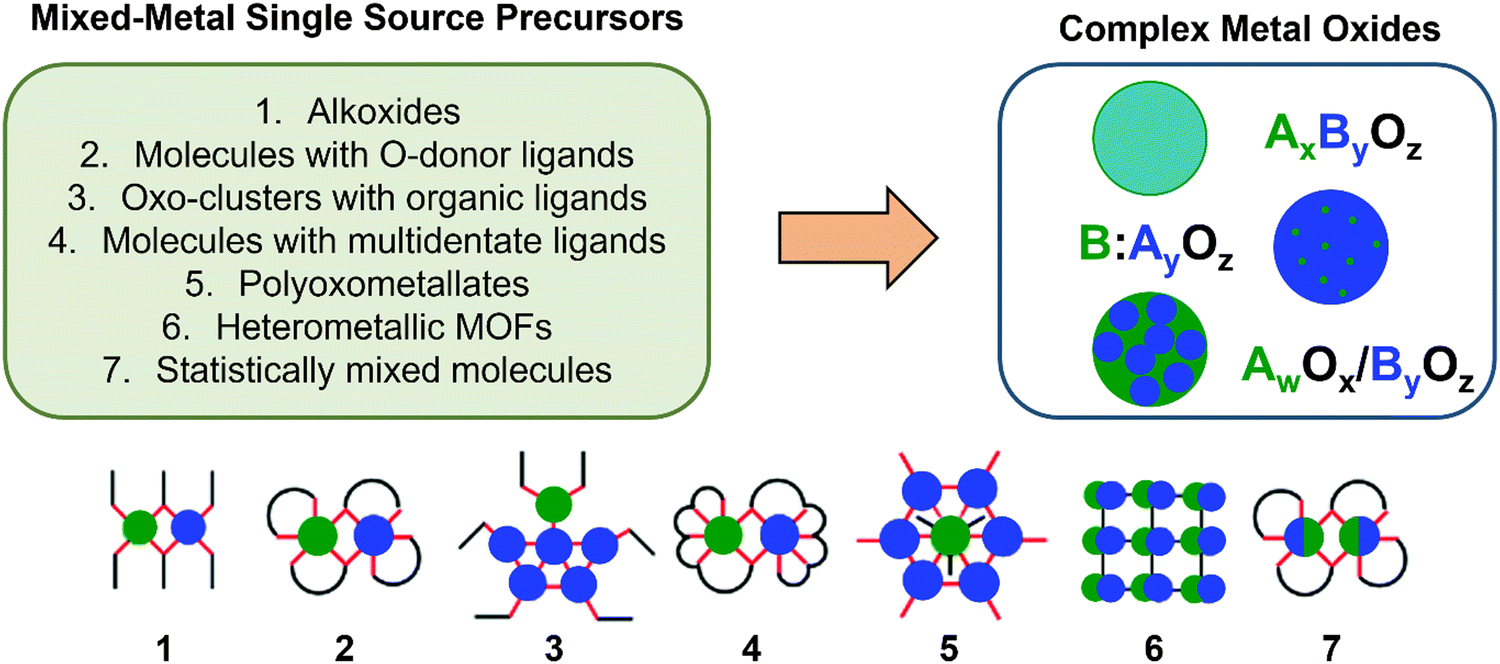 | ||
| Fig. 21 Structures for mixed-metal SSPs and the deposited complex metal oxides. Reproduced with permission from ref. 261 copyright 2020, Royal Society of Chemistry. | ||
There are two approaches towards SSP design for a multinuclear system: (i) binding many small, simple ligands individually to multinuclear centres; (ii) specifically designing a single, large ligand system that acts as a complex scaffold for multiple metal centres. Both can be effective, but the latter approach provides greater freedom in structural design and tailoring. Scaffolds can also be multi-use, with a range of metal atoms capable of integrating into the centre, hence a variety of doped or hybrid mixed metal semiconductors can be fabricated using a single ligand design, and without significantly altering the properties of the precursor which would require re-optimisation of the deposition conditions – a slow and expensive process.259,260
SSPs can be designed for three possible scenarios: (i) SSP-I, the stoichiometric ratio of elements in the SSP is equal to that in the deposit, but the number and structure of side products is not controlled (eqn (9)); (ii) SSP-II, same as SSP-I but with ligands that have been designed to decompose into fewer, inert and/or volatile side products (eqn (10)); (iii) SSP-III, the precursor decomposes to form two or more solid phases that make up the resulting composite deposit (eqn (11)).262
| ABnXY → ABn + X + Y | (9) |
| ABnXY → ABn + X–Y | (10) |
| ABnXY → ABn − m + mB + X–Y | (11) |
| Precursora | Material | Deposition technique | Nanostructure | Substrate/temp/solvent | j /mA cm−2 | Ref. |
|---|---|---|---|---|---|---|
| a Only the highest performing photoelectrode and precursor is listed from each literature report. b Photocurrent density measured at 0 V vs. RHE under 1 sun (100 mW cm−2, AM 1.5G) solar simulation, unless stated otherwise. All potentials are vs. RHE. | ||||||
| [Ti2(OEt)9(NiCl)]2 | NiOx/TiO2 | Spin coating | Smooth unfeatured | WO3/—/toluene | 0.45 | 98 |
| [Ti4Mo2O8(OEt)10]2 | Mo–TiO2 | Spray pyrolysis | Aggregated islands | FTO/150 (anneal 700)/toluene | 0.2 | 264 |
| [Bi2(DMSO)6V12O33Cl]2[Zn(DMSO)6] | Zn–BiVO4 | Drop casting | Mixed rods/particles | FTO/550/DMSO | 1.07 | 259 |
| [Mg2Ti4(O)2(OH)4(TFA)8(THF)6]·THF | MgTi2O5 | AACVD | Compact spheroid objects | FTO/600/EtOH | 0.25 | 247 |
| TFA = trifluoroacetato and THF = tetrahydrofuran | ||||||
| [Mn2Ti4(TFA)8(THF)6(OH)4(O)2]·0.4THF | Mn2O3–4TiO2 | AACVD | Uniform cube/rod distribution | FTO/450/THF | 0.343 | 265 |
| TFA = trifluoroacetato | ||||||
| {[CaMn(OAc)(TFA)3(THF)(H2O)2]·3THF}n (OAc = acetate, TFA = trifluoroacetate, THF = tetrahydrofuran) | Ca2Mn3O8–CaO | AACVD | Spheres | FTO/500/THF | 1.3 | 266 |
| [SrNb2(OiPr)12(HOiPr)] | SrNb2O6 | Electro-spinning | Nanofibers | —/1000 calcination/isopropanol | 0.16 | 267 |
| Zn6(OAc)8(μ-O)2(dmae)4 | ZnO | AACVD | Dense rectangular | FTO/400/THF | 0.09 | 268 |
| {Zn5(TFA)7(OH)2(H2O)4(OAc)}n·2(C4H6O2) | ZnO, Ag–ZnO | AACVD | ZnO: dense pyramidal particles | FTO/500/THF | ZnO: 0 at 0.8 V | 269 |
| [TFA = trifluoroacetate, OAc = acetate] | Ag–ZnO: porous rounded particle | Ag–ZnO: 0.55 at 0.8 V | ||||
| Ag(CH3COO) | ||||||
As noted in Section 3.1.2, pseudo-brookite structured Fe2TiO5 is a promising material for PEC water splitting, where purity can have a significant impact on the performance of the film, and therefore it makes sense to deposit using a SSP.276–279 Single-source deposited Fe2TiO5 appears difficult to produce as a phase pure material however, due to its high temperature of formation but low thermodynamic stability relative to its secondary phases, hematite and rutile.280,281 Soares et al. developed the [FeCl{Ti2(OPri)9}] precursor (Fig. 22) used in sol–gel deposition, which obtained films containing: (i) anatase TiO2 and amorphous Fe2O3 at 500 °C; (ii) rutile TiO2, α-Fe2O3, and pseudobrookite Fe2TiO5 at 700 °C; (iii) rutile TiO2 and pseudobrookite Fe2TiO5 at 1000 °C.282 Klabunde et al. reported similar issues with a range of metal titanates; using a [M{O–Ti(OPrn)3}2] (M = Mg, Mn, Fe, Co, Zn, Sn) precursor (Fig. 22b), composites of MTiO3/TiO2 were formed, except for M = Mg where pure pseudobrookite MgTi2O5 was obtained.283
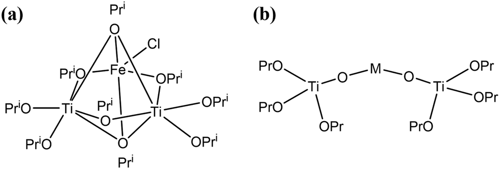 | ||
| Fig. 22 Molecular structures of (a) [FeCl{Ti2(OPri)9}], (b) [M{O–Ti(OPrn)3}2] (M = Mg, Mn, Fe, Co, Zn, Sn). | ||
Obtaining mixed phases from SSPs is often more common than single pure phases, previously defined as SSP-III. The precursor [NdAl3(OiPr)12(PriOH)] formed equimolar crystalline NdAlO3 and amorphous Al2O3 when applied in sol–gel and CVD techniques by Mathur et al.284,285 Mixed phase metal/metal oxides are also possible, for example, in work by Veith and Kneip, a BaSn2(OtBu)8 precursor used in MOCVD formed Sn and BaSnO3 mixed phases due to the disproportionation of the two valent Sn species to Sn(0) and Sn(IV).286 While single-source mixed-metal precursors have a greater occurrence of forming mixed phases due to the presence of multiple metal centres simultaneously depositing, it is important to note that it is not a unique characteristic and it is possible to fabricate similar mixed metal/metal oxide films from homo-nuclear precursors such as [Ge(OtBu)2]2, [Sn(OtBu)2]2, [Pb(OtBu)2]3 forming (α-Ge/GeO2), (β-Sn/SnO2), and (Pb/PbO2) respectively,287 and mixed phase metal oxide films such as rutile/anatase–TiO2 from [(EtO)Ti{OCMe2CH2}3N].288
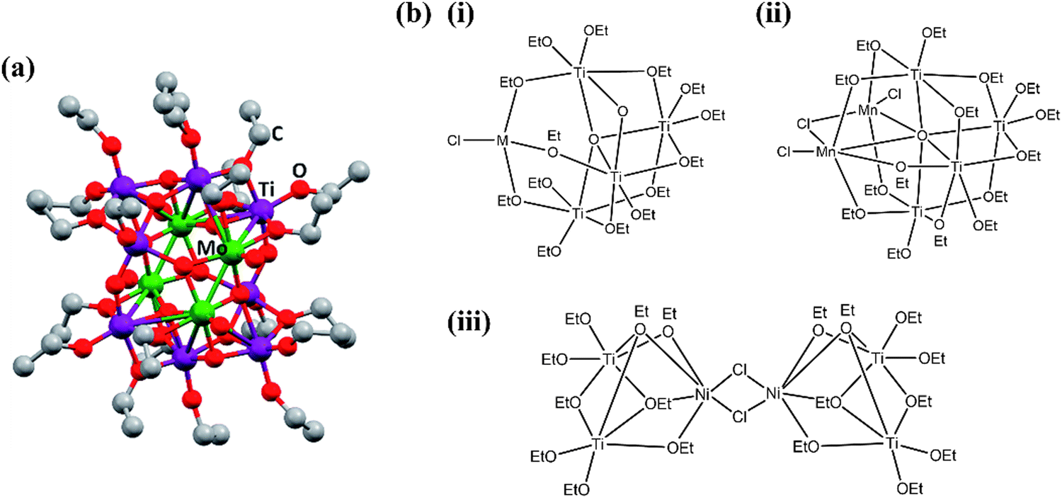 | ||
| Fig. 23 Molecular structures of (a) [Ti4Mo2O8(OEt)10]2, reproduced with permission from ref. 264 copyright 2018, Royal Society of Chemistry, (b) (i) [Ti4O(OEt)15(MCl)] (M = Co, Zn, Fe, Cu), (ii) [Ti4O(OEt)15(Mn2Cl3)], (iii) [Ti2(OEt)9(NiCl)]2. | ||
Similar work developed a family of heterometallic titanium oxo cage SSPs for different metal-doped TiO2 films using a simple solvothermal reaction of Ti(OEt)4 with a transition metal dichloride (MIICl2).260 The nature of the cage was dependent on the metal ion in each case due to differing ionic radii and strength of interactions, resulting in [Ti4O(OEt)15(MCl)] (M = Co, Zn, Fe, Cu), [Ti4O(OEt)15(Mn2Cl3)], and [Ti2(OEt)9(NiCl)]2 stoichiometries (Fig. 23), hence the doping stoichiometry for each will also be different within similar deposition parameters. Deposition studied using these precursors were not carried out.
Polyoxometallate (POM) cages of the form [MxOy(OR)z] are a promising solution-based precursor for thin film deposition due to the readily hydrolysable alkoxide groups, high solubility in organic solvents, and vast flexibility in molecular design.291 Modifications can be made to the structure to include functional ligands that will vary the thermal decomposition mechanism, and thus phase and morphology of the deposit,292,293 yield highly nanoporous or mesoporous films,294 or contain atoms for anionic doping (halides for example). Such structures are known as functional ligand-modified POMs (L-POM) with the formula [MxOy(OR)z(L)m] (OR = alkoxide, L = functional ligand). The yielded thin films are usually amorphous due to substantial amounts of organic residue because of poor decomposition from the L group, hence films require further calcination to remove carbon contamination and obtain crystalline films.295
Additional metal cations can be added into the structure of polyoxotitanates (POT) to form a metal-doped POT (M-POT, [TixOy(OR)zMnXm], M = metal ion, X = anion such as halide), which can act as a SSP to metal-doped materials. Importantly, M-POTs give a high degree of atomic control over the level of doping, for example, Wright et al. synthesised three Ce-POTs with structures [Ti28O38(OEt)38(EtOH)1.4CeCl], [Ti8O7(HOEt)(OEt)21Ce], and [{Ti2O(OEt)8}(EtOH·CeCl)]2 (Fig. 24) for use as Ce-doped TiO2 SSPs.296 [Ti28O38(OEt)38(EtOH)1.4CeCl] and [Ti8O7(HOEt)(OEt)21Ce] both contained high Ti:Ce ratios, 28:1 and 8:1 respectively, and yielded anatase TiO2 films with Ce doping at the exact concentrations matching the precursor stoichiometries. Interestingly, [{Ti2O(OEt)8}(EtOH·CeCl)]2, with a low Ti:Ce ratio (2:1), instead formed a phase separated TiO2-coated Ce2Ti2O7 film, implying that the inclusion of Ce(III) into the TiO2 lattice is concentration dependent. This behaviour has been reported for POTs multiple times, for example, in similar systems forming Ba-TiO2 and BaTiO2 from Ba-POT cages.297,298 The flexibility in choice of metal dopant makes these M-POT systems very promising SSP options for TiO2-based films, even facilitating lanthanide dopants such as Eu and Er.299,300
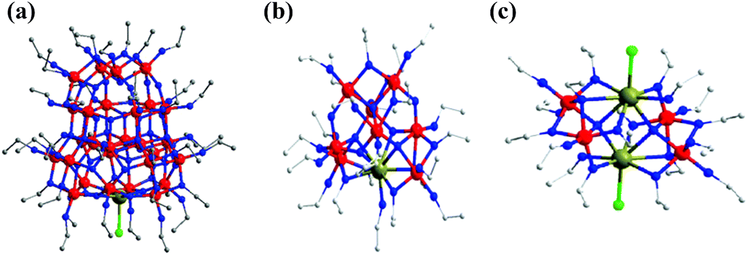 | ||
| Fig. 24 M-POT structures with varying Ti:Ce ratios, (a) [Ti28O38(OEt)38(EtOH)1.4CeCl], (b) [Ti8O7(HOEt)(OEt)21Ce], (c) [{Ti2O(OEt)8}(EtOH·CeCl)]2. Reproduced with permission from ref. 296 copyright 2013, Royal Society of Chemistry. | ||
Dopant ions can also be mobile in a material, allowing them to migrate to the surface of the electrode during operation and remain there for future use. This is particularly important when the dopant is an excellent electrocatalyst, as their surface enrichment provides a means of depositing a photoanode-electrocatalyst multi-component device with a single precursor in a single deposition step. Expanding on complexes designed by Streb et al.,302 Pike et al. synthesised a single-source trimetallic BiVO4 precursor that could use any one of a range of metal dopants; [Bi2(DMSO)6V12O33X]2[M(DMSO)6] (X = Cl, Br; M = Ca, Co, Ni, Cu, Zn).259 Aside from the impressive success of using an SSP to deposit doped BiVO4, the resulting Co-doped BiVO4 photoelectrode showed a surface (6–9 nm) enrichment of Co after initial operation, providing a concentrated Co surface layer in the photoelectrode, known to enhance PEC water oxidation and photoanode stability. Interestingly the Zn-doped BiVO4 film showed the greatest photocurrent response at 1.23 V vs. RHE (1.07 mA cm−2, Zn > Co > Cu > Ni > Undoped), but Co-doped showed the earliest onset potential (0.4 V vs. RHE) and the highest photocurrent at potentials lower than 1.15 V vs. RHE, due to the enhanced catalysis at the enriched Co surface. Zn is considered a structural modifier for BiVO4, hence a combination of Co and Zn dopants could combine the best properties of each of these M-doped films, since neither property is mutually exclusive. The Co-doped BiVO4 multi-component photoelectrode was then used in a scaled up 300 cm2 device, proving the method's viability for large scale production; a common flaw of many electrocatalyst loading techniques.
The efficiency of a catalyst is improved when used with a complementary material, for example, improved conductivity of NiOOH when combined with small fractions of FeOOH,303 Ca2+ stabilising water oxidation intermediates of CaMn4 clusters,304 or Fe forming a highly oxidised state to act as a favourable surface for oxidised ligands to form on during Co- or Ni-based catalysis.305 Zr is an emerging, unexplored partner to OER catalysts such as Co, providing protection from moisture as well as stabilisation of OER intermediates to reduce loss during catalysis. Novel SSPs with structures [{Zr4(μ4-O)(OEt)15}Co(II)Cl], [{Zr4(μ4-O)2(EtO)16}(Fe(III)Cl)2], [{Zr4(μ4-O)2(EtO)16}{(Cu(II)Cl)2(OEt)}2] were developed by Wright et al. for the solution deposition of catalyst-doped ZrO2 films.301 The Co-doped ZrO2 film had the lowest Tafel slopes and onset potentials (at pH 14, 1 M KOH electrolyte), as expected given Co is considered one of the most efficient non-precious metal oxidation catalysts available. All three doped films showed a stable, homogeneous distribution of catalyst dopant particles throughout ZrO2, an essential feature for electrocatalyst function as unstable dopant ions near the surface will be dissolved or reacted and the photoelectrode will lose the surface catalysis benefits.
| Precursora | Material | Deposition technique | Nanostructure | Substrate/temp/solvent | j /mA cm−2 | Ref. |
|---|---|---|---|---|---|---|
| a Only the highest performing photoelectrode and precursor is listed from each literature report. b Photocurrent density measured at 0 V vs. RHE under 1 sun (100 mW cm−2, AM 1.5G) solar simulation, unless stated otherwise. | ||||||
| [Sn(μ-NMe2){SC(NMe2)NC6H5}]2 | SnS | AACVD | 500 nm triangular grains | FTO/375 °C/toluene | −0.92 (470 nm illumination) | 242 |
| [{PhC(O)Se}2SnBu2] | SnSe | Hot injection + dropcasting | Nanosheets | FTO/200/isopropanol | −0.011 | 308 |
| [Sb{SeC(O)C6H5}3] | Sb2Se3 | Hot injection + dropcasting | Nanorod | FTO/200/isopropanol | −0.029, −0.662 at −0.6 VRHE | 125 |
| [Bi(SeOCPh)3] | Bi2Se3 | AACVD | Nanosheets | FTO/200/CHCl3 | −0.082, −0.213 at −0.6 VRHE | 309 |
Johnson et al. developed a family of 12 zinc thioureide systems, with general structures [{L}ZnMe], [{L}Zn{N(SiMe3)2}], and [{L}2Zn], where H{L} = iPrN(H)CS(NMe2), CyN(H)CS(NMe2), tBuN(H)CS(NMe2), or MesN(H)CS(NMe2), as SSPs to ZnS films, choosing AACVD to overcome the limitations seen with developing chalcogenide precursors with high volatilities for CVD.243 Viabilities for deposition were assessed by TGA. Many compounds showed multistep decompositions, with residual masses lower than ZnS, suggesting some volatility, or lower than ZnS and Zn, suggesting high volatility. Volatility is not an issue for AACVD, however, it hides the useful decomposition data from TGA traces. [{tBuN(H)CS(NMe2)}Zn{N(SiMe3)2}]2, showed the best TGA values (residual mass only 0.1% lower than extended, lowest onset temperature), but it contained a slow multi-step mass loss event after an initial rapid decrease. [{iPrN(H)CS(NMe2)}2Zn2] was therefore identified as the most promising for application due to its single mass loss event at low onset temperature, as well as practical benefits including ease of synthesis, stability, and solubility in THF – all factors that need to be considered outside of what is theoretically the best.
Johnson et al. have also synthesised and compared three SSPs for CdS deposition, pyridine, bis-3-methylpyridine and bis-4-methylpyridine complexes of cadmium(II) ethylxanthate ([Cd(S2COEt)2(Py)2], [Cd(S2COEt)2(3-MePy)2], [Cd(S2COEt)2(4-MePy)2] respectively).116 TGA profiles revealed single mass loss events for all three, however, the pyridine complex possessed the highest onset temperature and a residual mass significantly higher (11.5%) than that expected for CdS. The pyridine methyl compounds displayed similar thermograms, indicating that the position of the methyl group on the pyridine had negligible impact on thermal decomposition. Despite these similar TGA profiles however, the deposition of the methylpyridine derivatives were significantly different. The 3-MePy isomer grew dense aggregates of ∼200 nm particulates at both 220 and 350 °C process temperatures, while 4-MePy had plate-like morphologies at both temperatures with larger crystallite sizes of 25–36 nm compared to 16–17 nm. Further, the 3-MePy deposit had a hexagonal phase at both temperatures, with preferential growth in [002] direction, whereas that for 4-MePy was amorphous at 220 °C and hexagonal phase at 350 °C, again favouring the [002] direction. This clearly identifies the dramatic influence that minor precursor structure can make on the deposited film, in this case it is suggested that differences in the basicity and steric demands of the two isomeric derivatives are the cause of these differences.
Sb2Se3 is a very newly emerging photocathode material for PEC water splitting, despite its application in microelectronics predating this by several years. Sb2Te3 has also been recently applied towards PEC water splitting, but as a HER co-catalyst instead of photoelectrode.310 Reid et al. developed a series of alkylchalcogenostibines, [Me2SbSenBu], [MeSb(SenBu)2], [Sb(SenBu)3] as SSPs for Sb2Se3.311 LPCVD studies on all three precursors revealed [MeSb(SenBu)2] as the most promising based on Sb:Se ratios close to the desired 1:1.5 value, and superior uniformity and coverage of deposit, likely due to its higher volatility. Substrate-dependent morphologies were observed, producing a high surface area film consisting of separated clusters on SiO2, and a denser continuous thin film on TiN with lower surface area but higher surface coverage. Due to the success of this precursor, the tellurostibine analogue was synthesised as an SSP for Sb2Te3, requiring lower temperature for deposition (450 instead of 500 °C) but again seeing similar substrate-dependent morphologies, but on fused SiO2 compared to PVD silica.
5.4 Clusters
While they can lead to issues due to formation of many thermal decomposition fragments, higher required process temperatures, and worse air/moisture sensitivities, metal clusters can prove effective precursors, not only for their promise as multinuclear complexes for SSPs, but also producing interesting and more complex thin film morphologies and crystal phases, features which can enhance performance in many ways, as discussed in Section 4.1. There is also more flexibility in design for larger complexes, such as varying metal composition, nuclearity, spatial arrangements, and functionalities.312,313Eslava et al. used a Ti7O4(OEt)20 titanium-oxo cluster that produced a unique desert rose anatase TiO2 morphology when deposited using AACVD.139 This morphology was found to favour the (010) facet, the most photocatalytically active orientation for anatase, without the need for any templating, and produced an anatase phase that was impressively stable up to an annealing temperature of 1000 °C. To investigate the effect of the cluster precursor, its thermal decomposition was compared to that of a common titanium precursor, titanium ethoxide (Ti(OEt)4), in the same AACVD conditions. The simpler Ti(OEt)4 structure has in a single-step volatilisation, whereas [Ti7O4(OEt)20], as expected for a cluster, showed a more complex 3-step decomposition pathway that settled on the target TiO2 weight percentage (Fig. 25a and b). For [Ti(OEt)4], only the alkoxy groups must break off to reveal the Ti core for TiO2 growth, whereas in [Ti7O4(OEt)20] the alkoxy groups need to be removed, and the Ti–O–Ti bonds need to be broken. The resulting TiO2 morphologies can also be linked back to the difference in precursor structures, with [Ti(OEt)4] growing randomly distributed particles of irregular shape due to rapid decomposition, while [Ti7O4(OEt)20] grew the ordered and more complex structured desert rose, likely due to the influence of its large, sterically hindering ethoxide groups acting as barriers to growth around a single Ti growth site (Fig. 25c and d). As previously described in Section 4.1, the desert rose morphology also increases the light absorption efficiency due to reabsorption of scattered photons, particularly important for lighter/white coloured films such as TiO2.133
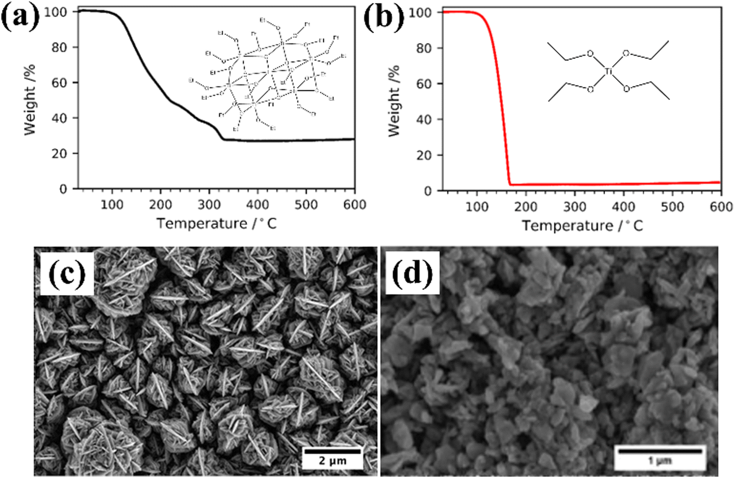 | ||
| Fig. 25 Thermogravimetric analysis data for (a) [Ti7O4(OEt)20], (b) [Ti(OEt)4], inserts show the respective molecular structures; and SEM micrographs of films deposited using 0.35 M concentration of precursors (c) [Ti7O4(OEt)20], (d) [Ti(OEt)4]. Reproduced with permission from ref. 139 copyright 2019, Royal Society of Chemistry. | ||
Another report by Eslava et al. used [Ti16O16(OEt)32] clusters with graphene oxide sacrificial templates to create nanoflakes that could act as spontaneous photocatalysts for hydrogen evolution when suspended in a methanol hole scavenging solution.314 This shows the versatility that polyoxometalate clusters possess for use within the PEC and PC field.
5.5 Polymorph control
The polymorph, or phase, of a deposited film is heavily influenced by the thermal decomposition pathway of the precursor, and the temperature along that pathway that the deposition process uses. Precursors with minor differences in molecular structure can therefore yield different polymorphs due to the differing decomposition pathways. Boyle et al. produced a series of calcium aryloxide precursors for the fabrication of calcium ceramics, and used thermogravimetric analysis (TGA) to explain the different polymorphs seen for different molecular structures (Fig. 26).315 Compound 3 (Fig. 26a) is seen to cleanly decompose (a single, fast mass loss event) in two distinct steps either side of the process temperature (200 °C), hence the precursor will decompose cleanly with no ongoing decomposition during the deposition. The flatter, stable section between the major mass-loss events at the process temperature favours a thermodynamically stable phase, which matches the portlandite phase seen experimentally, independent of the processing route.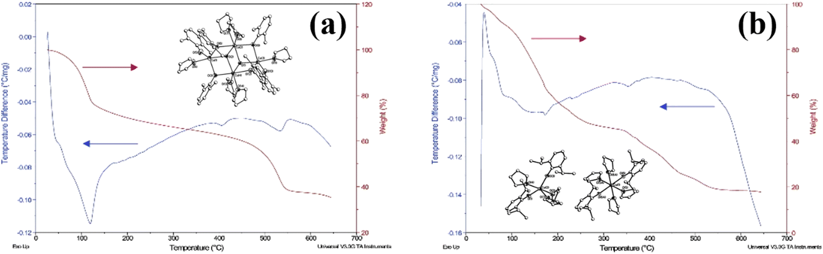 | ||
| Fig. 26 Differential thermal analysis (blue) and thermogravimetric analysis (red) traces for (a) compound 3, (b) compound 4a. Inserts show the molecular structures. Reproduced with permission from ref. 315 copyright 2007, American Chemical Society. | ||
Conversely, the TGA for compound 4a (Fig. 26b) contains many small weight steps with no stable, flat segments, indicating a more complex decomposition with many different steps and pathways. There are therefore ongoing decomposition events occurring at the process temperature, causing the kinetically favoured phases to be trapped instead of providing enough time for thermodynamic stability. Again, this was confirmed experimentally by the deposition of the vaterite phase when using compound 4a. To further confirm this phase-decomposition correlating theory, both precursors were deposited at elevated temperatures for prolonged times, now yielding the thermodynamically stable portlandite phase for both. This is as expected for compound 3 as it is already in the most stable state, and compound 4a now is being processed at a temperature above the more complex mass-loss events and instead in a smooth region on the TGA trace.
Exploring the exact thermal decomposition mechanism helps to understand how different polymorphs and purity can be selectively formed through chosen deposition temperature. Johnson et al. studied the thermal breakdown of a novel tin thioureide SnS precursor, [Sn(μ-NMe2){SC(NMe2)NC6H5}]2.242 Interestingly, deposits of α-SnS were formed at deposition temperatures of 375 °C, compared to ZB-SnS at 300 °C, which one may expect given that ZB-SnS is the thermodynamically unstable phase, but more kinetically stable phase, compared to α-SnS. TGA revealed a two-step thermal decomposition event (Fig. 27a), an initial minor drop at ∼270 °C followed by a rapid, complete drop to the expected residue that onsets during the first event but only reaches peak rate of mass loss at ∼315 °C. Using similar theory to that discussed by Boyle et al., using a process temperature that facilitates multiple ongoing decomposition events will trap the kinetically favoured phase, as is the case for 300 °C here. The precursor was found to form a dimer complex in solid state, however, evidence from high temperature (323 K) 119Sn NMR studies suggested that the dimer complex breaks down into its monomeric species at elevated temperatures. The nucleophilic {NMe2} group on the Sn centre is then free to attack the {NMe2} group at the central carbon. This was reinforced by the identification of a matching phenyl guanidine species by 13C NMR spectroscopy of the cold-trapped CVD by-products from a 375 °C deposition process, implying that at this temperature decomposition occurs in a single reaction step (Fig. 27b) likely matching the larger mass loss event seen in TGA, whereas at 300 °C there is contributions from another decomposition, however, the decomposition by-products at this temperature were not examined in the study.
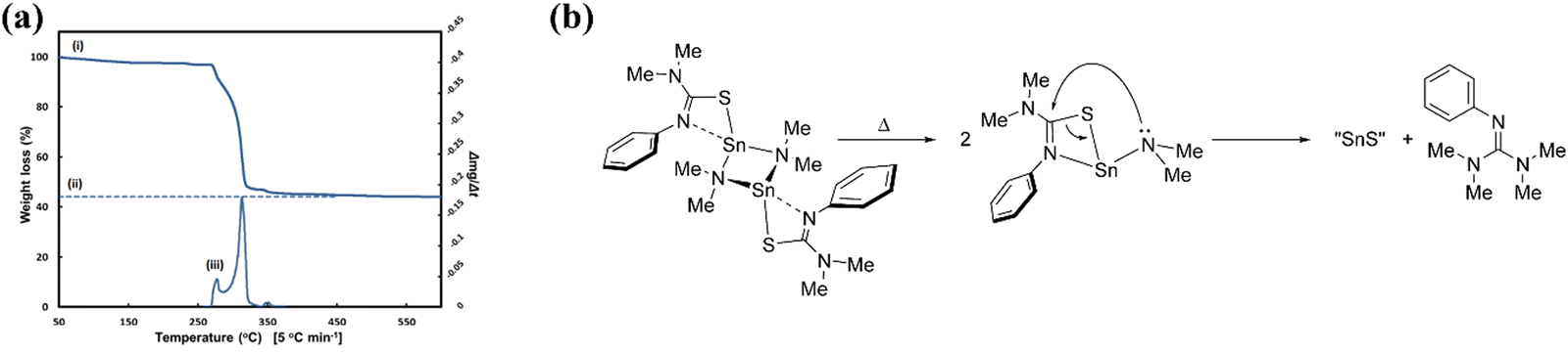 | ||
| Fig. 27 (a) TGA of [Sn(μ-NMe2){SC(NMe2)NC6H5}]2, and the derivative of mass loss with respect to temperature to identify significant mass loss events, (b) suggested SnS formation mechanism from initial precursor. Reproduced with permission from ref. 242 copyright 2015, American Chemical Society. | ||
5.6 Nanostructure control
Structural design of precursors is a key technique for controlling the morphology of thin films, particularly within multi-nuclear precursors where preferential film growth directions can be more easily controlled. The benefits of morphological control were outlined in Section 4.1.1. The precursor structure argument (PSA) treats precursors as building blocks to direct the final morphology formed, with many literature reports highlighting its effectiveness.316–319 Boyle et al. developed a Ca framework of 2 face-shared cubes, each with opposite corners missing (Fig. 28), depositing a nanorod morphology in both solution and solvothermal depositions.315 The organic moieties are removed during Ca deposition, leaving the double cubic structure which will grow significantly easier/faster in the direction where corners are not missing, fabricating particles with greater length in one direction than the other; rods. Similar ZnO work expands on this structural argument for the influence of the central multi-nuclear core of the precursors, using Zn cores with increasing nuclearity and steric size to deposit nanorod morphologies with increasing rod thickness to match the core structure.319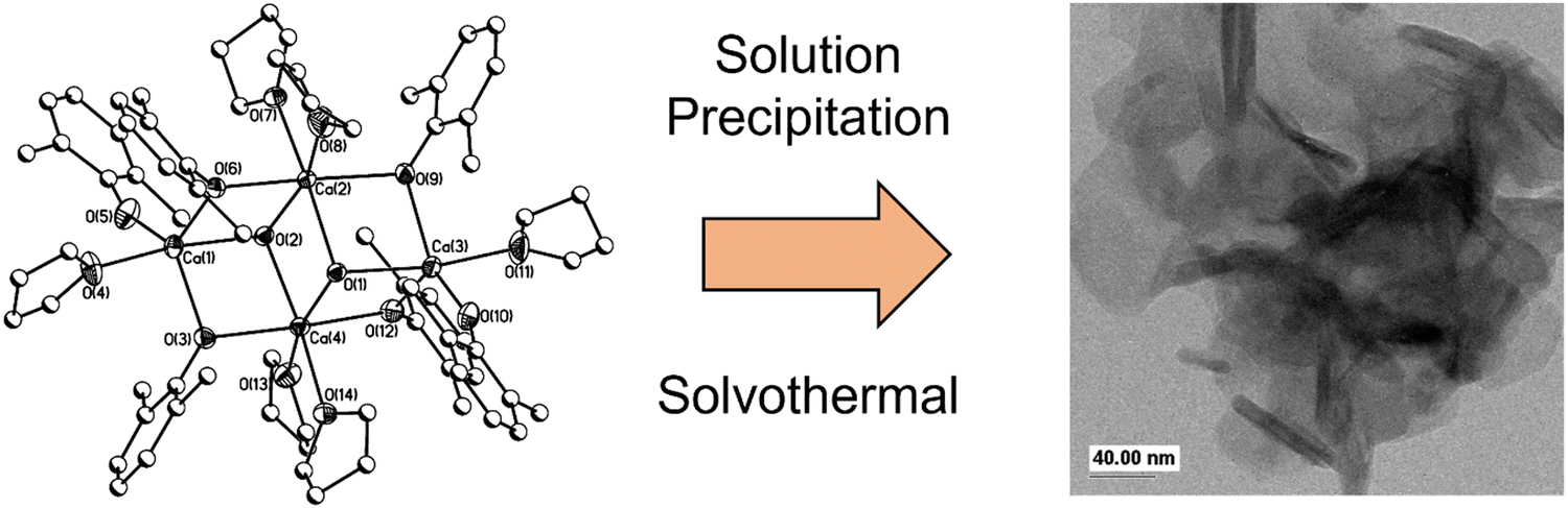 | ||
| Fig. 28 Structure plot of a Ca framework designed to fabricate nanorod morphology, with TEM image of a nanorod cluster produced via solution precipitation route. Reproduced with permission from ref. 315 copyright 2007, American Chemical Society. | ||
Cd chalcogen precursors have also been used to a similar extent,318 showing how morphological changes are possible based on the influence of decomposition by-products which poison and promote different growth planes, however, the ability to control this outside of trial and error is limited. The chalcogen used (S, Se, Te) also impacted the final morphology (sphere, rod, sphere respectively), hence the control of the morphology relies on all different parameters within the precursor molecular structure: metal core structure, ligand choice and its decomposition fragments, and the chalcogen (or oxygen) choice for M–L bonding.
An option for controlling film morphology through precursor molecular structure without requiring multi-nuclear complexes is with multidentate ligands with strong M–L bonds, for example, M-alkoxide bonds as described previously. The slower thermal decomposition process means that at any instance during film growth, when the metal centre has bound to the substrate or growing film surface, each M–L bond will break in distinct, time separated events, leaving the ligand, or remaining fragment of ligand, bound but in a different position around the metal and occupying space within the growing film, therefore creating a porous structure.288 This method has less control over the exact shape of the nanostructure morphology; however, it is complementary with previously described benefits to chelating ligands, and can be achieved with low-nuclear complexes.
To effectively control elongated morphology (essential for high surface area, thicker films), the rate of nucleation site generation during precursors decomposition must be limited, while maintaining sufficient feedstock to continue growth, and without the process taking too long or requiring too much precursor.320 Highly reactive precursors lead to rapid deposition, but an overload of nucleation sites results in uncontrolled film growth.317 The use of the stronger M–O bonds compared to M–N tends to favour this reduction in reactivity just enough for controlled growth, however, it may vary depending on the ligand, the metal, and the amount of steric hindrance.
6. Further photoelectrode performance enhancement
So far, the review has detailed ways to design and tailor molecular precursors to deposit a high-performance film with controlled and desired properties. To make a competitive photoelectrode, additional, post-deposition modifications can and must be made to further increase performance and maximise efficiencies. There are numerous approaches that can be applied to increase the complexity of the device, and usually a combination of many will be used. Here, the three most common methods will be outlined, however, there are countless other modifications that can be made, including sensitizer incorporation, deposition of a blocking layer, protective layer, passivating layer and charge transport layer, and tandem cell configurations.6.1 Heterojunction formation
Charge carrier recombination is a dominant source of efficiency loss in most photochemical devices, but one common and highly effective method for enhancing the properties of a device against this is by layering one semiconductor on top of another, known as a heterojunction, or composite semiconductor. There are many variations of heterojunctions, distinguished in two ways: (i) whether the majority charge carriers present in each semiconductor are the same (p–p or n–n heterojunction) or opposite (p–n or n–p heterojunction), known as isotype and anisotype heterojunctions respectively;321 (ii) by the relative band positions of each semiconductor (Fig. 29), if both bands of one semiconductor are straddled by those of the other, it is Type-I, if only one of the VB or CB of one semiconductor is straddled by both bands of the other, it is Type-II, and if one has both bands above the CB of the other, it is Type-III.322 Type-I heterojunctions show no improvement to charge carrier separation since all carriers are accumulated onto semiconductor B, whereas Type-II and Type-III junctions result in spatially separated holes and electrons, reducing recombination and increasing lifetimes.323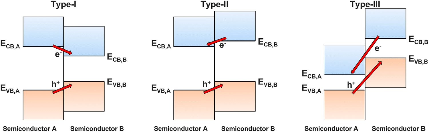 | ||
| Fig. 29 Variations of heterojunction based on energy band alignments. | ||
Further, heterojunctions can be created for multiple functions, such as employing a protective layer that has compatible band positioning, or using a second semiconductor with a significantly different band gap that will absorb photons of energy too low for the original semiconductor, or too large resulting in energy losses to nonradiative relaxation, hence utilising the available photon energy range more efficiently. It is important to note that the second semiconductor layer used to create the heterojunction can also be designed using bespoke precursors as outlined in Section 5, resulting in two or more semiconductors developed and optimised in this way. The additional layer should therefore be fabricated on its own first to ensure the best precursor structure and deposition conditions/technique are found prior to layering.
ALD is an outstanding technique for depositing heterojunction layers due in part to its high aspect ratio deposition, meaning the carefully designed, high surface area morphology of the initial semiconductor layer is not filled by the second material, but rather uniformly coated to maintain shape and surface area. The highly controllable thickness of deposition is also essential for optimisation of the two layers, as often the second layer in a heterojunction is only there for charge separation and surface passivation. It is also a chemisorption-based process, ensuring intimate contact between the layers and hence more rapid carrier injection across the interface.56,324–326
In recent work by Johnson et al., a TiO2 nanorod system was coated with NiO using ALD to form a TiO2/NiO heterojunction, yielding significantly increased photocurrents at all potentials and a conformal NiO coating was observed that maintained the morphology and high porosity of the TiO2 nanorods (Fig. 30).327 Barecca et al. used ALD to coat TiO2 onto a chemical vapour deposited Fe2O3 film, forming an intimately contacted TiO2-stabilised heterojunction with a 10-fold photocurrent increase due to the enhanced charge separation and transfer.328,329 ALD can also be used to deposit hybrid materials using either single-source or dual-source precursors. Fe2TiO5, for example, was deposited onto an Fe2O3 film to increase photocurrent performance by up to 3.5-fold.330
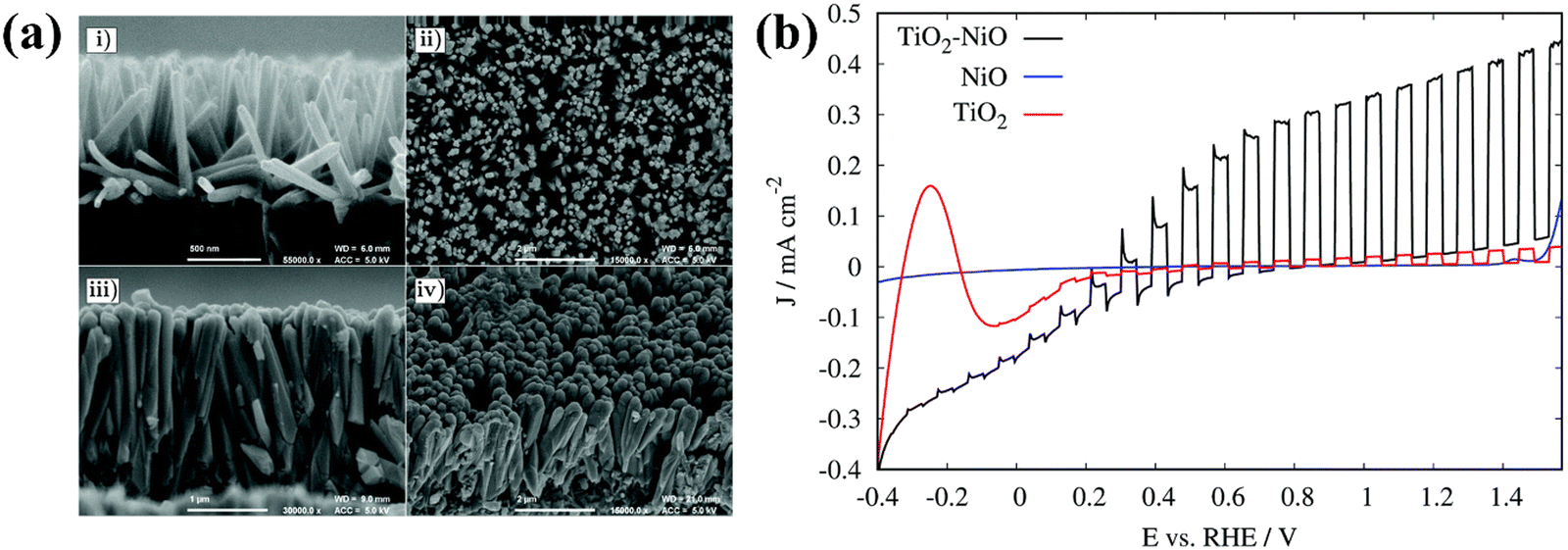 | ||
| Fig. 30 (a) Scanning electron microscopy images of TiO2 nanorods before (above) and after (below) NiO ALD coating, (b) photocurrent densities measured under chopped 1 sun rear-side illumination for TiO2, NiO, and NiO-coated TiO2 systems. Reproduced with permission from ref. 327 copyright 2021, Royal Society of Chemistry. | ||
6.2 Annealing
Post deposition annealing is a useful tool to remove carbon contamination from the deposition, increase the crystallinity of the film to increase conductance, alter film or nanoparticle shape and size, and convert the material phase to a more thermodynamically favoured phase.95 Annealing can also be undergone in a range of environments to modify the oxygen content within the film in whichever direction is required for that material. An air environment is oxidative, hence oxygen deficient as-deposited films can be air-annealed to ensure correct stoichiometry.231 Annealing in a vacuum or hydrogen environment is reductive, hence it is possible to increase the oxygen deficit/number of oxygen vacancies which can enhance PEC properties of some metal oxides, such as charge carrier generation and separation, by effective vacancy doping.331 TiO2, which forms Ti3+ centres with oxygen vacancies, has been reported to have significantly greater PEC performance after hydrogen or vacuum annealing, and vacuum annealing has also been shown by Marken et al. to change the material selectivity from oxygen evolution to chorine evolution in the presence of chloride ions.13,1516.3 Co-catalyst loading
The principles of co-catalyst loading have already been covered in Section 4.2, and it should be stated that for almost any real-world device it is essential to have co-catalysts, however, what form this takes can vary between thin films, nanoparticles, and surface-level doping. Thin films are often the chosen option when the co-catalyst has greater stability than the pristine film, good charge transport properties, and preferential energy band alignment with the material below, for example, with WO3-coated BiVO4, such that the loading not only improves surface charge transfer, but also acts as a protective layer and a component in a heterojunction for enhanced bulk charge transfer.92,332Catalyst doping, particularly at the surface, can be used to combine the enhancement associated with doped materials (i.e. narrower bandgap, better charge transport, reduced recombination) with the improved surface transfer and catalysis kinetics associated with co-catalysts, however, it is only viable for catalyst species that are compatible for doping with the bulk material, and when the bulk material is already chemically stable enough during operation since additional protective layers will render the catalyst dopant pointless.333,334 Case studies for SSP catalyst doping were covered in Section 5.3.5. It also facilitates the fabrication of the overall device in fewer steps without the need for a separate process to load catalyst on the surface, which is always preferential when moving towards commercialisation. Finally, nanoparticles are typically the only option when precious metal catalysts are required, since the high cost and rarity limits the quantity of metal that can be used for a realistic device, while still providing as many active sites through exposed catalyst surface area as possible.335,336
Deposition of cocatalysts often uses common precursors and simple methods, however, the same principles for precursor design may be taken into consideration to design an efficient co-catalyst loading process, either as a distinct additional deposition process or in the same process as photoelectrode deposition. Table 7 shows examples of literature reporting novel precursor design of electrocatalysts for water splitting.
| Precursor | Material | Deposition technique | Catalytic activity | Overpotentiala | Tafel slopeb | Ref. |
|---|---|---|---|---|---|---|
| a Overpotential measured at 10 (−10) mA cm−2 for the OER (HER)/mV. b Tafel slope measured at 10 (−10) mA cm−2 for the OER (HER)/mV dec−1. | ||||||
| FeMn(CO)8(μ-PH(μ-PH2) | FeMnP | MOCVD | OER | 280 | 57 | 337 |
| [Ni4(HL)4(OAc)4] | NiOx | Electrodeposition | OER | 380–400 | 42 | 338 |
| H2L = 2,6-pyridinedimethanol | ||||||
| [Ti2(OEt)9(NiCl)]2 | NiOx/TiO2 | Spin coating | OER | Increased WO3 photocurrent at low bias | — | 98 |
| [Ir(COD)(DPAMD)] | Ir | MOCVD | OER and HER | HER: 50 | HER: 41 | 339 |
| COD = 1,5-cyclooctadiene | ||||||
| DPAMD = N,N′-diisopropyl-amidinate | ||||||
| [Bi(SeOCPh)3] | Bi2Se3 | AACVD | OER and HER | OER: 385 | OER: 122 | 309 |
| HER: 220 | HER: 178 | |||||
| [{Zr4(μ4-O)(OEt)15}CoIICl] | Co–ZrO2 | Solution deposition | OER | 430 | 54 | 301 |
Devi et al. used three Ir precursors (Fig. 31) that had been tailored for high volatility and thermal stability to suit deposition via MOCVD, and to create a highly catalytically efficient Ir coating method for oxygen evolution enhancement.339 Thermal evaluation of each precursor by TGA led to conclusion of [Ir(COD)(DPAMD)] being the most promising, owing to its decomposition to the residual weight of crystalline metallic Ir (confirmed by PXRD) at suitably low temperatures. By varying the deposition time from 3.25 min to 30 min, the microstructure of the deposits was controllable, ranging from nanoparticulate deposition to a continuous thin film respectively, allowing for tailoring of the electrocatalyst form to suit the underlying material, as discussed earlier in the section.
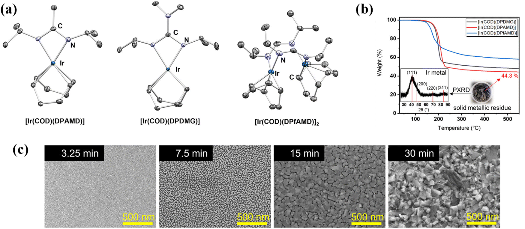 | ||
| Fig. 31 (a) Structures of three bespoke Ir precursors, (b) TGA curves for the three complexes with PXRD of the residue for [Ir(COD)(DPAMD)], (c) SEM images of the Ir film deposited from [Ir(COD)(DPAMD)] with varying deposition times. Reproduced with permission from ref. 339 copyright 2022, American Chemical Society. | ||
Coupling co-catalysts with complementary materials can enhance their effectiveness. Zr-based mixed metal oxides are an emerging system for use in stable, low-cost, and earth abundant electrocatalyst coatings. Zr4+ has a high charge density, making it strongly Lewis acidic, a trait known to stabilise water oxidation intermediates during catalysis.340,341 It is therefore promising to couple Zr with an effective OER catalyst, such as Co, into a single mixed-metal oxide system for improving surface water oxidation at the photoanode. Wright et al. developed three SSPs, [Zr4O(EtO)15Co(II)Cl], [Zr4(O)2(EtO)16Fe2(III)Cl2], [Zr4(O)2(EtO)18Cu4(II)Cl4], for the deposition of first-row transition metal-doped ZrO2 thin films Co–ZrO2, Fe–ZrO2, Cu–ZrO2 respectively, as discussed in Section 5.5.5.301
7. Overall device design and characterisation
The most significant device properties, design methods to control them, and techniques to measure each are outlined in Table 8. It should be noted that molecular precursor design can influence all these properties, as discussed throughout Section 5, however, for a commercial device it is beneficial to combine precursor design with other techniques to obtain vastly greater performances than any device design method could on its own.| Device property to enhance | Design method | Measurement technique |
|---|---|---|
| Light absorption | Heterojunction | PEC efficiency (STH, IPCE) |
| Doping | UV/Vis spectroscopy (Tauc plot – bandgap measurement) | |
| Nanostructure | ||
| Bulk charge separation | Heterojunction | Impedance |
| Doping | Mott Schottky plot (charge carrier density) | |
| Morphology (surface area, nanostructure, orientation) | ||
| Surface charge transfer | Co-catalyst loading | Hole/electron quencher PEC measurements |
| Doping | ||
| Interface passivation | ||
| Grain size | Nucleation rate, annealing | XRD (Scherrer equation) |
| Bulk carrier mobility | Annealing | Impedance |
| Doping | ||
| Morphology (surface area, nanostructure, orientation) | Templating, additives, deposition method and conditions (temp., prec. conc., solvent) | SEM, TEM, EBSD |
| Chemical and photo-stability | Protective layer | Chronoamperometry |
| Electrolyte choice | ||
| Material phase/polymorph | Temperature of deposition and annealing | XRD |
| Raman spectroscopy | ||
8. Conclusions and outlook
8.1 Summary
The most crucial factor affecting the composition and structure of a semiconductor is the precursor itself.244 Bespoke precursor development for semiconducting thin films is a well explored field, with the overwhelming benefits already proven in areas such as microelectronics, however, it has yet to be significantly introduced to PEC water splitting, despite similarities in many design requirements. Similarly, extensive PEC studies on complex multi-component devices are reported regularly, but using untailored, commercially available precursors for material fabrication. The quality of research and expertise within these two fields individually is exceptional, hence if collaborations can be made to link the two areas together, the potential research output could have remarkable impact, producing higher performance devices as well as using a more systematic, informed approach to gain valuable knowledge for the benefit of future development and progression.The ligand structure on a precursor not only influences its own properties for tailoring towards specific deposition techniques and conditions, but also the resulting deposit structure, composition, and performance. The thermal decomposition and removal of the ligand is therefore key to precursor development. The molecular structure should provide the precursor with favourable properties for handling and deposition, while being thermally decomposed and removed rapidly at low temperatures, ideally as a gas phase by-product or an inert species that will not act as a contaminant source, react with starting precursor, or negatively impact the crystal growth. The more complex the precursor, the greater the complexity of thermal decomposition and fragmentation, which can be detrimental to film growth, but can also result in unique physical properties that are unseen in standard common precursor uses.
The general requirements of any precursor, novel or not, are purity, stability, low-toxicity, ease and scale of synthesis, and cost. From there, specialised precursors can be designed to target more tailored properties, such as thermal decomposition kinetics and pathways, volatility/solubility, deposit morphology, deposit crystal phase and orientation, and homogeneity in single and mixed materials. The physical features of the photoelectrode, such as morphology and polymorph composition, are becoming increasingly important as research advances. The use of templating, additives, etching, and post-deposition treatment can achieve good control over these properties; however, all these options also increase production time and costs, limiting scalability. Tailored precursors offer excellent control over the physical features of the deposit without the need for additional fabrication steps or chemicals, vastly increasing the potential for scaling to commercial and industrial application.
Precursor development is not necessarily reliant on planning the perfect structure from the start, but instead designing a base structure that should provide the desired properties, followed by ongoing refinement of this structure to progressively achieve more effective performance in optimal deposition conditions, and composition and structure of the photoelectrode deposited. Such refinement processes are not possible with commercial, pre-made precursors. Several case studies that exemplify this iterative structure refinement have been discussed throughout the review.
Transition from lab scale to commercial must be considered when designing new precursors and materials if the technology is to become viable. High STH efficiencies are not industrially meaningful unless the device can be effectively scaled to yield high H2 production rates. Both the precursor synthesis and the deposition techniques must therefore be chosen carefully to ensure suitability for batch production across large surface areas. CVD techniques have been proven for large scale production already, and are well suited to the use of new and multiple precursors, hence it is likely that CVD will dominate material production in the future, and why it has been the focus of this review compared to alternative deposition methods.
Herein, it has been described how bespoke precursor development is an invaluable tool for the tailored optimisation of each property within a semiconductor. Compatibility between precursors is required for doping, hybridisation, and any other simultaneous use, which is more effective and more easily controlled using molecular structures that have been specifically designed for simultaneous use. Alternatively, single-source precursors can overcome many issues associated with combining multiple individual precursors, such as a simpler deposition process, fewer film defects, and greater homogeneity of deposition, however, the multinuclear, larger complexes used requires an even greater focus and control on molecular structure and behaviour; hence such precursors are usually only effective when they have been well-designed for purpose, which demands a strong understanding of, and consideration towards, design requirements. This field can therefore be expanded by the inclusion of synthetic chemists and collaboration between an interdisciplinary team, splitting photoelectrode development and characterisation into: (i) planning and design of the desired material(s)/electrode; (ii) bespoke precursor synthesis; (iii) precursor deposition; film characterisation, and iterative optimisation; (iv) photoelectrochemical characterisation; and (v) additional complexity towards an overall multicomponent photoelectrode device (Fig. 32).
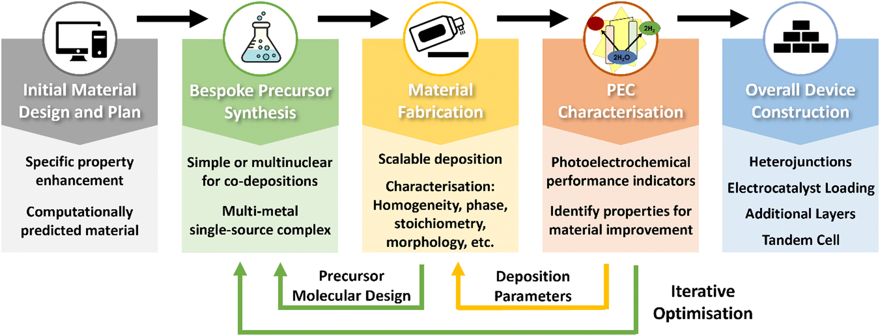 | ||
| Fig. 32 An idealised complete interdisciplinary workplan and work packages for photoelectrode development. | ||
The current absence of work on tailoring for water splitting photoelectrodes provides clear and strong evidence for the importance and timeliness of this review, highlighting the benefits of tailored precursors towards: (i) suitability for deposition and optimising required deposition conditions; (ii) resulting thin film properties that can enhance overall water splitting performance; (iii) providing unique properties to thin films that are unseen in commercial precursors; (iv) progressive, iterative improvements to precursors; (v) gaining more valuable long-term knowledge and understanding from systematic precursor designs for future development. All this together shows that the only way to achieve the target of a cost-effective, stable, highly efficient PEC device is by combining the expertise available across a range of disciplines.
8.2 Future outlook
The overall aim for this field is to create a highly efficient PEC device that is cost-effective and stable long-term.59 It has been concluded that individual semiconductors are not capable of this – TiO2 is cheap and stable but has poor carrier generation, BiVO4 is effective at carrier generation but has slow bulk and surface transport, Cu2O has high PEC efficiencies but is unstable. It is therefore clear that not only does each material need to be maximised in its own performance, combinations of materials through doping, hybridisation, layering, and co-catalyst loading will be essential to achieving this target. At present, there is a significant disparity between theoretical maximum efficiency and practical performance, particularly in photoanodes which are limited by the sluggish OER kinetics. The only way to achieve the development of new, better, and more complex materials, using existing deposition techniques, is through new, systematic precursor design. This would switch to a more ‘bottom-up’, fundamental approach towards systematic photoelectrode material development, focusing on the development and optimisation of individual materials, using suitable precursors such that they can be combined to then fabricate more complex devices with already highly optimised individual components. The use of techniques such as AACVD allows for greater precursor design flexibility, particularly for large, complex, multinuclear precursors that can be used as SSPs for advanced materials.Consequently, new materials are emerging as promising next generation photoelectrodes to either replace or supplement the more ubiquitous materials such as TiO2. In fact, there is excellent compatibility between bespoke precursor design and the fabrication requirements for many of these next generation materials. Hybrid and complex materials such as Fe2TiO5,342 perovskites,343 and organic polymers344 are among the alternatives. Additionally, computational studies can be used to predict new materials with a myriad of multi-metal elemental compositions as promising next generation photoelectrodes.345–347 It is therefore clear that having a library of already compatible precursors for a wide range of different metal species which can be dropped in and instantly used effectively would be invaluable, not only for reducing the time required to develop an optimised process for each new material, but also improve the quality of deposition using precursors already tailored for this function. In this way, computationally predicted new materials can be quickly and effectively experimentally screened as potential candidates, and those that show promise can then be examined further, with additional tailored precursors, including SSPs, being synthesised specifically for property optimisation of that individual material.
High entropy and entropy-stabilised inorganic materials are a recent development, but show great promise in a range of energy and catalysis applications, including photoelectrochemical water splitting.348 Often containing greater than five principal metal elements incorporated into a single disordered phase, this class of materials show unique and promising structures and properties conducive towards use in highly efficient photoelectrodes.349 Current synthesis procedures use high temperature and multi-stepped methods, often using solid state synthetic strategies from the constituent elements, however, simpler and more scalable routes using metal precursors have also been explored, for example in the work by Lewis et al.,350 where precursors were decomposed in tandem to form a high entropy transition metal disulfide material (Fig. 33).351,352 The simultaneous application of a collection of bespoke and compatible metal precursors, or the development of a multinuclear SSP containing five or more different metals, could be an effective, scalable fabrication route for these materials, particularly with a lower temperature deposition technique such as AACVD followed by high temperature post-treatment to ensure single-phase formation.
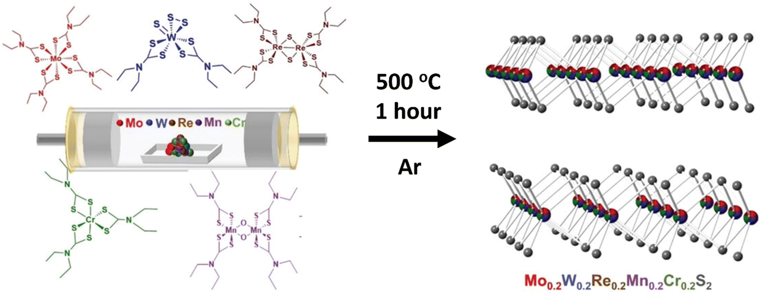 | ||
| Fig. 33 Schematic of the preparation of a high entropy transition metal disulfide by the thermal decomposition of five precursor powders in tandem. Reproduced with permission from ref. 350 copyright 2023, Wiley-VCH. | ||
All-in-all, the PEC water splitting field is currently dominated by materials scientists and electrochemists, however, there is a large absence of precursor design for material development, which requires inorganic chemists to fill, if the technology is to progress further and become viable and successful. This inter-disciplinary approach is an untapped research field, ripe for further development and discovery; and it will only grow in both size and importance as green hydrogen is increasingly introduced and integrated into society. Now is the time to get involved and realise its potential. This review links the two sides of PEC water splitting to encourage a more inter-disciplinary approach that can push PEC water splitting into new frontiers of understanding and performance.
List of abbreviations
| 0D, 1D, 2D, 3D | Zero/one/two/three-dimensional |
| AACVD | Aerosol-assisted chemical vapour deposition |
| ALD | Atomic layer deposition |
| a-TiO2 | Amorphous TiO2 |
| CB | Conduction band |
| CBM | Conduction band minima |
| CBTS | Cu2BaSnS4 |
| COD | 1,5-Cyclooctadiene |
| CVD | Chemical vapour deposition |
| CZTS | Cu2ZnSnS4 |
| DCM | Dichloromethane |
| DME | Dimethoxyethane |
| DMSO | Dimethylsulfoxide |
| DPAMD | N,N′-Diisopropyl-amidinate |
| EBSD | Electron backscatter diffraction |
| EIS | Electrochemical impedance spectroscopy |
| Et | Ethyl group |
| FE | Faradaic efficiency |
| FTO | Fluorine-doped tin oxide |
| GC-MS | Gas chromatography–mass spectroscopy |
| HER | Hydrogen evolution reaction |
| HOMO | Highest occupied molecular orbital |
| IPCE | Incident photon to current conversion efficiency |
| iPr | Isopropyl group |
| LPCVD | Low-pressure CVD |
| LUMO | Lowest unoccupied molecular orbital |
| Me | Methyl group |
| MI-IR | Matrix-isolation infrared (spectroscopy) |
| MOCVD | Metal–organic chemical vapour deposition |
| M-POT | Metal-doped polyoxotitanate |
| NMR | Nuclear magnetic resonance (spectroscopy) |
| OAc | Acetate |
| OER | Oxygen evolution reaction |
| PC | Photocatalysis |
| PEC | Photoelectrochemical |
| Ph | Phenyl group |
| POM | Polyoxometalate |
| POT | Polyoxotitanate |
| PSA | Precursor structure argument |
| PV | Photovoltaics |
| PV–E | Coupled photovoltaics–electrolysis |
| PXRD | Powder X-ray diffraction |
| Py | Pyridine |
| RHE | Reversible hydrogen potential |
| SEM | Scanning electron microscopy |
| SHE | Standard hydrogen potential |
| SSP | Single-source precursor |
| STH | Solar to hydrogen conversion efficiency |
| t Bu | tert-Butyl group |
| TEM | Transmission electron microscopy |
| TFA | Trifluoroacetate |
| TGA | Thermogravimetric analysis |
| THF | Tetrahydrofuran |
| TMP | Transition metal phosphine |
| VB | Valence band |
| VBM | Valence band maxima |
| XRD | X-ray diffraction |
List of symbols
| E | Potential |
| e− | Electron |
| E F | Fermi level |
| E redox | Electrolyte redox potential |
| h+ | Hole |
| j photo | Photocurrent density |
| V on | Onset potential |
| V plat | Plateau potential |
| φ ox | Oxidation potential |
| φ red | Reduction potential |
Conflicts of interest
There are no conflicts to declare.Acknowledgements
We gratefully acknowledge the financial support of the University of Bath and University of Monash, and the provision of a Bath/Monash PhD studentship to T. R. H. L.; C. L. B. is the recipient of an Australian Research Council (ARC) Discovery Early Career Researcher Award (DECRA, project number DE200101076), funded by the Australian Government.References
- Energy Institute, 72nd Statistical Review of World Energy, 2023.
- J. Tsao, N. Lewis and G. Crabtree, Solar FAQs, US Department Energy, 2006, 1–24 Search PubMed.
- S. Wang, A. Lu and C.-J. Zhong, Nano Convergence, 2021, 8, 4 CrossRef CAS PubMed.
- W. Yang, R. R. Prabhakar, J. Tan, S. D. Tilley and J. Moon, Chem. Soc. Rev., 2019, 48, 4979–5015 RSC.
- N. Nitta, F. Wu, J. T. Lee and G. Yushin, Mater. Today, 2015, 18, 252–264 CrossRef CAS.
- G. Girishkumar, B. McCloskey, A. C. Luntz, S. Swanson and W. Wilcke, J. Phys. Chem. Lett., 2010, 1, 2193–2203 CrossRef CAS.
- I. Staffell, D. Scamman, A. V. Abad, P. Balcombe, P. E. Dodds, P. Ekins, N. Shah and K. R. Ward, Energy Environ. Sci., 2019, 12, 463–491 RSC.
- J. Chi and H. Yu, Chin. J. Catal., 2018, 39, 390–394 CrossRef CAS.
- M. K. Singla, P. Nijhawan and A. S. Oberoi, Environ. Sci. Pollut. Res., 2021, 28, 15607–15626 CrossRef CAS PubMed.
- D. J. Durbin and C. Malardier-Jugroot, Int. J. Hydrogen Energy, 2013, 38, 14595–14617 CrossRef CAS.
- Internal Atomic Energy Agency, Hydrogen Production Using Nuclear Energy, 2013.
- Z. Li, S. Fang, H. Sun, R. J. Chung, X. Fang and J. H. He, Adv. Energy Mater., 2023, 13, 1–26 Search PubMed.
- T. R. Harris-Lee, Y. Zhang, C. R. Bowen, P. J. Fletcher, Y. Zhao, Z. Guo, J. W. F. Innocent, S. A. L. Johnson and F. Marken, Electrocatalysis, 2021, 12, 65–77 CrossRef CAS.
- C. Palmer, F. Saadi and E. W. McFarland, ACS Sustainable Chem. Eng., 2018, 6, 7003–7009 CrossRef CAS.
- B. Mei, G. Mul and B. Seger, Adv. Sustainable Syst., 2017, 1, 1600035 CrossRef.
- S. Chen, D. Huang, P. Xu, W. Xue, L. Lei, M. Cheng, R. Wang, X. Liu and R. Deng, J. Mater. Chem. A, 2020, 8, 2286–2322 RSC.
- A. Raveendran, M. Chandran and R. Dhanusuraman, RSC Adv., 2023, 13, 3843–3876 RSC.
- L. Tian, X. Guan, S. Zong, A. Dai and J. Qu, Catalysts, 2023, 13, 355 CrossRef CAS.
- Q. Chen, G. Fan, H. Fu, Z. Li and Z. Zou, Adv. Phys. X, 2018, 3, 1487267 Search PubMed.
- T. Hisatomi and K. Domen, Nat. Catal., 2019, 2, 387–399 CrossRef CAS.
- K. Takanabe, ACS Catal., 2017, 7, 8006–8022 CrossRef CAS.
- C. Ros, T. Andreu and J. R. Morante, J. Mater. Chem. A, 2020, 8, 10625–10669 RSC.
- B. D. Alexander, P. J. Kulesza, I. Rutkowska, R. Solarska and J. Augustynski, J. Mater. Chem., 2008, 18, 2298–2303 RSC.
- S. Ardo, D. Fernandez Rivas, M. A. Modestino, V. Schulze Greiving, F. F. Abdi, E. Alarcon Llado, V. Artero, K. Ayers, C. Battaglia, J. P. Becker, D. Bederak, A. Berger, F. Buda, E. Chinello, B. Dam, V. Di Palma, T. Edvinsson, K. Fujii, H. Gardeniers, H. Geerlings, S. M. Hashemi, S. Haussener, F. Houle, J. Huskens, B. D. James, K. Konrad, A. Kudo, P. P. Kunturu, D. Lohse, B. Mei, E. L. Miller, G. F. Moore, J. Muller, K. L. Orchard, T. E. Rosser, F. H. Saadi, J. W. Schüttauf, B. Seger, S. W. Sheehan, W. A. Smith, J. Spurgeon, M. H. Tang, R. Van De Krol, P. C. K. Vesborg and P. Westerik, Energy Environ. Sci., 2018, 11, 2768–2783 RSC.
- C. Jiang, S. J. A. Moniz, A. Wang, T. Zhang and J. Tang, Chem. Soc. Rev., 2017, 46, 4645–4660 RSC.
- M. G. Walter, E. L. Warren, J. R. McKone, S. W. Boettcher, Q. Mi, E. A. Santori and N. S. Lewis, Chem. Rev., 2010, 110, 6446–6473 CrossRef CAS PubMed.
- B. D. Alexander, P. J. Kulesza, I. Rutkowska, R. Solarska and J. Augustynski, J. Mater. Chem., 2008, 18, 2298–2303 RSC.
- T. Hisatomi and K. Domen, Nat. Catal., 2019, 2, 387–399 CrossRef CAS.
- S. K. Ghosh and H. Rahaman, Noble Metal-Metal Oxide Hybrid Nanoparticles, Elsevier, 2019, pp. 313–340 Search PubMed.
- R. Tang, S. Zhou, Z. Zhang, R. Zheng and J. Huang, Adv. Mater., 2021, 33, 2005389 CrossRef CAS PubMed.
- M. S. Prévot and K. Sivula, J. Phys. Chem. C, 2013, 117, 17879–17893 CrossRef.
- C. Jiang, S. J. A. Moniz, A. Wang, T. Zhang and J. Tang, Chem. Soc. Rev., 2017, 46, 4645–4660 RSC.
- P. Hofmann, Solid State Physics: an introduction, 2nd edn, 2015 Search PubMed.
- R. J. Singh, Solid State Physics, Pearson, India, 1st edn, 2011 Search PubMed.
- H. Ibach and H. Lüth, Solid-state physics: An introduction to principles of materials science, Springer Berlin Heidelberg, 2010 Search PubMed.
- A. B. Bocarsly and H. Tachikawa, in Laboratory Techniques in Electroanalytical Chemistry, Revised and Expanded, ed. P. Kissinger and W. R. Heineman, Taylor and Francis Ltd., 2nd edn, 1996, pp. 855–899 Search PubMed.
- M. Shakeel, B. Li, M. Arif, G. Yasin, W. Rehman, A. U. Khan, S. Khan, A. Khan and J. Ali, Appl. Catal., B, 2018, 227, 433–445 CrossRef CAS.
- J. W. Harder, J. M. Fontenla, P. Pilewskie, E. C. Richard and T. N. Woods, Geophys. Res. Lett., 2009, 36, L07801 CrossRef.
- X. Tao, Y. Zhao, S. Wang, C. Li and R. Li, Chem. Soc. Rev., 2022, 51, 3561–3608 RSC.
- Y. Ma, X. Wang, Y. Jia, X. Chen, H. Han and C. Li, Chem. Rev., 2014, 114, 9987–10043 CrossRef CAS PubMed.
- J. Li and N. Wu, Catal. Sci. Technol., 2015, 5, 1360–1384 RSC.
- M. R. Nellist, F. A. L. Laskowski, F. Lin, T. J. Mills and S. W. Boettcher, Acc. Chem. Res., 2016, 49, 733–740 CrossRef CAS PubMed.
- S. M. Thalluri, L. Bai, C. Lv, Z. Huang, X. Hu and L. Liu, Adv. Sci., 2020, 7, 1902102 CrossRef CAS PubMed.
- H. Eidsvåg, S. Bentouba, P. Vajeeston, S. Yohi and D. Velauthapillai, Molecules, 2021, 26, 1–30 CrossRef PubMed.
- J. Low, J. Yu, M. Jaroniec, S. Wageh and A. A. Al-Ghamdi, Adv. Mater., 2017, 29, 1601694 CrossRef PubMed.
- J. R. Hook and H. E. Hall, Solid state physics, 2nd edn, 1928 Search PubMed.
- Z. Chen, H. N. Dinh and E. Miller, Photoelectrochemical Water Splitting Standards, Experimental Methods, and Protocols, 2013 Search PubMed.
- B. Klahr, S. Gimenez, F. Fabregat-Santiago, J. Bisquert and T. W. Hamann, Energy Environ. Sci., 2012, 5, 7626–7636 RSC.
- F. Spadavecchia, S. Ardizzone, G. Cappelletti, L. Falciola, M. Ceotto and D. Lotti, J. Appl. Electrochem., 2013, 43, 217–225 CrossRef CAS.
- L. M. Peter, A. B. Walker, T. Bein, A. G. Hufnagel and I. Kondofersky, J. Electroanal. Chem., 2020, 872, 114234 CrossRef CAS.
- K. Schwarzburg and F. Willig, Appl. Phys. Lett., 1991, 58, 2520–2522 CrossRef CAS.
- Z. Chen, T. F. Jaramillo, T. G. Deutsch, A. Kleiman-Shwarsctein, A. J. Forman, N. Gaillard, R. Garland, K. Takanabe, C. Heske, M. Sunkara, E. W. McFarland, K. Domen, E. L. Milled and H. N. Dinh, J. Mater. Res., 2010, 25, 3–16 CrossRef CAS.
- S. Zhang, I. Ahmet, S. H. Kim, O. Kasian, A. M. Mingers, P. Schnell, M. Kölbach, J. Lim, A. Fischer, K. J. J. Mayrhofer, S. Cherevko, B. Gault, R. Van De Krol and C. Scheu, ACS Appl. Energy Mater., 2020, 3, 9523–9527 CrossRef CAS PubMed.
- C. Y. Toe, Z. Zheng, H. Wu, J. Scott, R. Amal and Y. H. Ng, Angew. Chem., 2018, 130, 13801–13805 CrossRef.
- C. Y. Toe, J. Scott, R. Amal and Y. H. Ng, J. Photochem. Photobiol., C, 2019, 40, 191–211 CrossRef CAS.
- N. Pastukhova, A. Mavrič and Y. Li, Adv. Mater. Interfaces, 2021, 8, 2002100 CrossRef CAS.
- F. E. Osterloh, Chem. Mater., 2008, 20, 35–54 CrossRef CAS.
- Y. J. Jang and J. S. Lee, ChemSusChem, 2019, 12, 1835–1845 CrossRef CAS PubMed.
- C. Jiang, S. J. A. Moniz, A. Wang, T. Zhang and J. Tang, Chem. Soc. Rev., 2017, 46, 4645–4660 RSC.
- K. Qi, S. Liu and A. Zada, J. Taiwan Inst. Chem. Eng., 2020, 109, 111–123 CrossRef CAS.
- P. Lianos, Appl. Catal., B, 2017, 210, 235–254 CrossRef CAS.
- A. Fujishima and K. Honda, Nature, 1972, 238, 37–38 CrossRef CAS PubMed.
- Z. Zhang, L. Zhang, M. N. Hedhili, H. Zhang and P. Wang, Nano Lett., 2012, 13, 14–20 CrossRef PubMed.
- I. S. Cho, C. H. Lee, Y. Feng, M. Logar, P. M. Rao, L. Cai, D. R. Kim, R. Sinclair and X. Zheng, Nat. Commun., 2013, 4, 1–10 Search PubMed.
- M. Xu, P. Da, H. Wu, D. Zhao and G. Zheng, Nano Lett., 2012, 12, 1503–1508 CrossRef CAS PubMed.
- K. Rajeshwar, N. R. de Tacconi and C. R. Chenthamarakshan, Chem. Mater., 2001, 13, 2765–2782 CrossRef CAS.
- K. Basu, H. Zhang, H. Zhao, S. Bhattacharya, F. Navarro-Pardo, P. K. Datta, L. Jin, S. Sun, F. Vetrone and F. Rosei, Nanoscale, 2018, 10, 15273–15284 RSC.
- J. N. Tiwari, R. N. Tiwari and K. S. Kim, Prog. Mater. Sci., 2012, 57, 724–803 CrossRef CAS.
- J. Joy, J. Mathew and S. C. George, Int. J. Hydrogen Energy, 2018, 43, 4804–4817 CrossRef CAS.
- O. K. Varghese and C. A. Grimes, Sol. Energy Mater. Sol. Cells, 2008, 92, 374–384 CrossRef CAS.
- S. Cho, J.-W. Jang, K.-H. Lee and J. S. Lee, APL Mater., 2014, 2, 010703 CrossRef.
- V. Etacheri, C. Di Valentin, J. Schneider, D. Bahnemann and S. C. Pillai, J. Photochem. Photobiol., C, 2015, 25, 1–29 CrossRef CAS.
- F. Niu, D. Wang, F. Li, Y. Liu, S. Shen and T. J. Meyer, Adv. Energy Mater., 2020, 10, 1900399 CrossRef.
- M. Pelaez, N. T. Nolan, S. C. Pillai, M. K. Seery, P. Falaras, A. G. Kontos, P. S. M. Dunlop, J. W. J. Hamilton, J. A. Byrne, K. O’Shea, M. H. Entezari and D. D. Dionysiou, Appl. Catal., B, 2012, 125, 331–349 CrossRef CAS.
- T. Luttrell, S. Halpegamage, J. Tao, A. Kramer, E. Sutter and M. Batzill, Sci. Rep., 2014, 4, 1–8 Search PubMed.
- J. E. S. Haggerty, L. T. Schelhas, D. A. Kitchaev, J. S. Mangum, L. M. Garten, W. Sun, K. H. Stone, J. D. Perkins, M. F. Toney, G. Ceder, D. S. Ginley, B. P. Gorman and J. Tate, Sci. Rep., 2017, 7, 1–11 CrossRef CAS PubMed.
- X. Chen, L. Liu, P. Y. Yu and S. S. Mao, Science, 2011, 331, 746–750 CrossRef CAS PubMed.
- Z. Wang, C. Yang, T. Lin, H. Yin, P. Chen, D. Wan, F. Xu, F. Huang, J. Lin, X. Xie and M. Jiang, Energy Environ. Sci., 2013, 6, 3007–3014 RSC.
- S. Das, S. H. Kim, Y. K. Park, C. M. Choi, D. Y. Kim and Y. B. Hahn, Mater. Chem. Phys., 2010, 124, 704–708 CrossRef CAS.
- A. R. Bally, E. N. Korobeinikova, P. E. Schmid, F. Lévy and F. Bussy, J. Phys. D: Appl. Phys., 1998, 31, 1149–1154 CrossRef CAS.
- V. C. Anitha, A. N. Banerjee and S. W. Joo, J. Mater. Sci., 2015, 50, 7495–7536 CrossRef CAS.
- E. Parzinger, B. Miller, B. Blaschke, J. A. Garrido, J. W. Ager, A. Holleitner and U. Wurstbauer, ACS Nano, 2015, 9, 11302–11309 CrossRef CAS PubMed.
- Z. Li, X. Meng and Z. Zhang, J. Photochem. Photobiol., C, 2018, 35, 39–55 CrossRef CAS.
- A. Bak, W. Choi and H. Park, Appl. Catal., B, 2011, 110, 207–215 CrossRef CAS.
- E. Kalamaras, V. Dracopoulos, L. Sygellou and P. Lianos, Chem. Eng. J., 2016, 295, 288–294 CrossRef CAS.
- P. S. Bassi, S. Y. Chiam, Gurudayal, J. Barber and L. H. Wong, ACS Appl. Mater. Interfaces, 2014, 6, 22490–22495 CrossRef CAS PubMed.
- M. A. Melo, H. A. Centurion, T. T. A. Lucas, D. N. F. Muche, F. L. Souza and R. V. Gonçalves, ACS Appl. Nano Mater., 2020, 3, 9303–9317 CrossRef CAS.
- S. Kment, F. Riboni, S. Pausova, L. Wang, L. Wang, H. Han, Z. Hubicka, J. Krysa, P. Schmuki and R. Zboril, Chem. Soc. Rev., 2017, 46, 3716–3769 RSC.
- L. Wang, N. T. Nguyen, X. Huang, P. Schmuki and Y. Bi, Adv. Funct. Mater., 2017, 27, 1703527 CrossRef.
- A. Kudo, K. Ueda, H. Kato and I. Mikami, Catal. Lett., 1998, 53, 229–230 CrossRef CAS.
- Z. Li, W. Luo, M. Zhang, J. Feng and Z. Zou, Energy Environ. Sci., 2013, 6, 347–370 RSC.
- B. S. Kalanoor, H. Seo and S. S. Kalanur, Mater. Sci. Energy Technol., 2021, 4, 317–328 CAS.
- K. Sayama, A. Nomura, Z. Zou, R. Abe, Y. Abe and H. Arakawa, Chem. Commun., 2003, 2908–2909 RSC.
- J. Gan, X. Lu and Y. Tong, Nanoscale, 2014, 6, 7142–7164 RSC.
- X. Liu, F. Wang and Q. Wang, Phys. Chem. Chem. Phys., 2012, 14, 7894–7911 RSC.
- S. Sfaelou, L. C. Pop, O. Monfort, V. Dracopoulos and P. Lianos, Int. J. Hydrogen Energy, 2016, 41, 5902–5907 CrossRef CAS.
- M. Sarnowska, K. Bienkowski, P. J. Barczuk, R. Solarska and J. Augustynski, Adv. Energy Mater., 2016, 6, 1600526 CrossRef.
- Y. H. Lai, T. C. King, D. S. Wright and E. Reisner, Chem. – Eur. J., 2013, 19, 12943–12947 CrossRef CAS PubMed.
- B. D. Alexander, P. J. Kulesza, I. Rutkowska, R. Solarska and J. Augustynski, J. Mater. Chem., 2008, 18, 2298–2303 RSC.
- Q. Huang, Z. Ye and X. Xiao, J. Mater. Chem. A, 2015, 3, 15824–15837 RSC.
- C. G. Read, Y. Park and K. S. Choi, J. Phys. Chem. Lett., 2012, 3, 1872–1876 CrossRef CAS PubMed.
- Y. Liu, F. Le Formal, F. Boudoire, L. Yao, K. Sivula and N. Guijarro, J. Mater. Chem. A, 2019, 7, 1669–1677 RSC.
- M. S. Prévot, Y. Li, N. Guijarro and K. Sivula, J. Mater. Chem. A, 2016, 4, 3018–3026 RSC.
- S. P. Berglund, F. F. Abdi, P. Bogdanoff, A. Chemseddine, D. Friedrich and R. Van De Krol, Chem. Mater., 2016, 28, 4231–4242 CrossRef CAS.
- C. G. Morales-Guio, S. D. Tilley, H. Vrubel, M. Gratzel and X. Hu, Nat. Commun., 2014, 5, 1–7 Search PubMed.
- A. Paracchino, V. Laporte, K. Sivula, M. Grätzel and E. Thimsen, Nat. Mater., 2011, 10, 456–461 CrossRef CAS PubMed.
- T. Shi, Y. Feng, Y. Zhong, H. Ding, K. Chen and D. Chen, Inorganics, 2023, 11, 155 CrossRef CAS.
- J. Yin, J. Jin, H. Lin, Z. Yin, J. Li, M. Lu, L. Guo, P. Xi, Y. Tang and C. Yan, Adv. Sci., 2020, 7, 1903070 CrossRef CAS PubMed.
- Y. Chen, X. Feng, M. Liu, J. Su and S. Shen, Nanophotonics, 2016, 5, 524–547 Search PubMed.
- L. Zheng, F. Teng, X. Ye, H. Zheng and X. Fang, Adv. Energy Mater., 2020, 10, 1–32 Search PubMed.
- I. Y. Ahmet, J. R. Thompson and A. L. Johnson, Eur. J. Inorg. Chem., 2018, 1670–1678 CrossRef CAS.
- H. Lee, W. Yang, J. Tan, J. Park, S. G. Shim, Y. S. Park, J. W. Yun, K. M. Kim and J. Moon, ACS Appl. Mater. Interfaces, 2020, 12, 15155–15166 CrossRef CAS PubMed.
- I. Y. Ahmet, M. S. Hill, P. R. Raithby and A. L. Johnson, Dalton Trans., 2018, 47, 5031–5048 RSC.
- M. Yarema, R. Caputo and M. V. Kovalenko, Nanoscale, 2013, 5, 8398–8410 RSC.
- D. V. Talapin, J. S. Lee, M. V. Kovalenko and E. V. Shevchenko, Chem. Rev., 2010, 110, 389–458 CrossRef CAS PubMed.
- M. A. Buckingham, A. L. Catherall, M. S. Hill, A. L. Johnson and J. D. Parish, Cryst. Growth Des., 2017, 17, 907–912 CrossRef CAS.
- J. A. Nasir, Z. U. Rehman, S. N. A. Shah, A. Khan, I. S. Butler and C. R. A. Catlow, J. Mater. Chem. A, 2020, 8, 20752–20780 RSC.
- A. Kolivand and S. Sharifnia, Int. J. Energy Res., 2021, 45, 2739–2752 CrossRef CAS.
- S. Han, Y. C. Pu, L. Zheng, L. Hu, J. Z. Zhang and X. Fang, J. Mater. Chem. A, 2016, 4, 1078–1086 RSC.
- L. Xu, J. Meng, J. Wang, L. Wang and Q. Li, New J. Chem., 2022, 46, 8079–8087 RSC.
- P. Adams, F. Creazzo, T. Moehl, R. Crockett, P. Zeng, Z. Novotny, S. Luber, W. Yang and S. D. Tilley, J. Mater. Chem. A, 2023, 11, 8277–8284 RSC.
- J. Kim, W. Yang, Y. Oh, H. Lee, S. Lee, H. Shin, J. Kim and J. Moon, J. Mater. Chem. A, 2017, 5, 2180–2187 RSC.
- L. Zhang, Y. Li, C. Li, Q. Chen, Z. Zhen, X. Jiang, M. Zhong, F. Zhang and H. Zhu, ACS Nano, 2017, 11, 12753–12763 CrossRef CAS PubMed.
- W. Yang, S. Lee, H. C. Kwon, J. Tan, H. Lee, J. Park, Y. Oh, H. Choi and J. Moon, ACS Nano, 2018, 12, 11088–11097 CrossRef CAS PubMed.
- M. D. Khan, M. Aamir, M. Sohail, M. Sher, J. Akhtar, M. A. Malik and N. Revaprasadu, Sol. Energy, 2018, 169, 526–534 CrossRef CAS.
- J. Ge, Y. Yu and Y. Yan, ACS Energy Lett., 2016, 1, 583–588 CrossRef CAS.
- J. Ge, P. J. Roland, P. Koirala, W. Meng, J. L. Young, R. Petersen, T. G. Deutsch, G. Teeter, R. J. Ellingson, R. W. Collins and Y. Yan, Chem. Mater., 2017, 29, 916–920 CrossRef CAS.
- R. B. Hall, R. W. Birkmire, J. E. Phillips and J. D. Meakin, Appl. Phys. Lett., 1981, 38, 925–926 CrossRef CAS.
- M. V. Makarova, F. Amano, S. Nomura, C. Tateishi, T. Fukuma, Y. Takahashi and Y. E. Korchev, ACS Catal., 2022, 12, 1201–1208 CrossRef CAS.
- A. Prathan, C. Bhoomanee, P. Ruankham, S. Choopun, A. Gardchareon, S. Phadungdhitidhada and D. Wongratanaphisan, Mater. Today Proc., 2019, 17, 1514–1520 CrossRef CAS.
- S. Reghunath, D. Pinheiro and K. R. Sunaja Devi, Appl. Surf. Sci. Adv., 2021, 3, 100063 CrossRef.
- Y. Zhou, L. Zhang, L. Lin, B. R. Wygant, Y. Liu, Y. Zhu, Y. Zheng, C. B. Mullins, Y. Zhao, X. Zhang and G. Yu, Nano Lett., 2017, 17, 8012–8017 CrossRef CAS PubMed.
- M. Ge, C. Cao, J. Huang, S. Li, Z. Chen, K.-Q. Zhang, S. S. Al-Deyab and Y. Lai, J. Mater. Chem. A, 2016, 4, 6772–6801 RSC.
- D. Li, Y. Liu, W. Shi, C. Shao, S. Wang, C. Ding, T. Liu, F. Fan, J. Shi and C. Li, ACS Energy Lett., 2019, 4, 825–831 CrossRef CAS.
- H. S. Han, S. Shin, D. H. Kim, I. J. Park, J. S. Kim, P. S. Huang, J. K. Lee, I. S. Cho and X. Zheng, Energy Environ. Sci., 2018, 11, 1299–1306 RSC.
- R. Li, F. Zhang, D. Wang, J. Yang, M. Li, J. Zhu, X. Zhou, H. Han and C. Li, Nat. Commun., 2013, 4, 1–7 Search PubMed.
- J. Pan, G. Liu, G. Q. (Max) Lu and H.-M. Cheng, Angew. Chem., Int. Ed., 2011, 50, 2133–2137 CrossRef CAS PubMed.
- T. R. Gordon, M. Cargnello, T. Paik, F. Mangolini, R. T. Weber, P. Fornasiero and C. B. Murray, J. Am. Chem. Soc., 2012, 134, 6751–6761 CrossRef CAS PubMed.
- M. Regue, S. Sibby, I. Y. Ahmet, D. Friedrich, F. F. Abdi, A. L. Johnson and S. Eslava, J. Mater. Chem. A, 2019, 7, 19161–19172 RSC.
- J. Du, M. Zhang and J. Tian, Int. J. Miner., Metall. Mater., 2022, 29, 49–58 CrossRef CAS.
- H. Kmentova, S. Kment, L. Wang, S. Pausova, T. Vaclavu, R. Kuzel, H. Han, Z. Hubicka, M. Zlamal, J. Olejnicek, M. Cada, J. Krysa and R. Zboril, Catal. Today, 2017, 287, 130–136 CrossRef CAS.
- A. K. Singh and D. Sarkar, Nanoscale, 2018, 10, 13130–13139 RSC.
- T. Li, H. Jin, Z. Liang, L. Huang, Y. Lu, H. Yu, Z. Hu, J. Wu, B. Y. Xia, G. Feng and J. Zhou, Nanoscale, 2018, 10, 6844–6849 RSC.
- X. Xiao, H. Song, S. Lin, Y. Zhou, X. Zhan, Z. Hu, Q. Zhang, J. Sun, B. Yang, T. Li, L. Jiao, J. Zhou, J. Tang and Y. Gogotsi, Nat. Commun., 2016, 7, 1–8 Search PubMed.
- I. Vladimirov, M. Kühn, T. Geßner, F. May and R. T. Weitz, Sci. Rep., 2018, 8, 1–10 CAS.
- J. Wang and C. Jiang, Org. Electron., 2014, 16, 164–170 CrossRef.
- R. T. Weitz, K. Amsharov, U. Zschieschang, M. Burghard, M. Jansen, M. Kelsch, B. Rhamati, P. A. Van Aken, K. Kern and H. Klauk, Chem. Mater., 2009, 21, 4949–4954 CrossRef CAS.
- R. T. Weitz, K. Amsharov, U. Zschieschang, E. B. Villas, D. K. Goswami, M. Burghard, H. Dosch, M. Jansen, K. Kern and H. Klauk, J. Am. Chem. Soc., 2008, 130, 4637–4645 CrossRef CAS PubMed.
- W. Kalb, P. Lang, M. Mottaghi, H. Aubin, G. Horowitz and M. Wuttig, Synth. Met., 2004, 146, 279–282 CrossRef CAS.
- D. C. Hurum, A. G. Agrios, K. A. Gray, T. Rajh and M. C. Thurnauer, J. Phys. Chem. B, 2003, 107, 4545–4549 CrossRef CAS.
- T. R. Harris-Lee, S. A. L. Johnson, L. Wang, P. J. Fletcher, J. Zhang, C. Bentley, C. R. Bowen and F. Marken, New J. Chem., 2022, 46, 8385–8392 RSC.
- K. Sivula, J. Phys. Chem. Lett., 2013, 4, 1624–1633 CrossRef CAS PubMed.
- M. Zhong, T. Hisatomi, Y. Kuang, J. Zhao, M. Liu, A. Iwase, Q. Jia, H. Nishiyama, T. Minegishi, M. Nakabayashi, N. Shibata, R. Niishiro, C. Katayama, H. Shibano, M. Katayama, A. Kudo, T. Yamada and K. Domen, J. Am. Chem. Soc., 2015, 137, 5053–5060 CrossRef CAS PubMed.
- O. Zandi and T. W. Hamann, J. Phys. Chem. Lett., 2014, 5, 1522–1526 CrossRef CAS PubMed.
- F. Le Formal, S. R. Pendlebury, M. Cornuz, S. D. Tilley, M. Grätzel and J. R. Durrant, J. Am. Chem. Soc., 2014, 136, 2564–2574 CrossRef CAS PubMed.
- H. Lee, W. Yang, J. Tan, Y. Oh, J. Park and J. Moon, ACS Energy Lett., 2019, 4, 995–1003 CrossRef CAS.
- Y. Mi and Y. Weng, Sci. Rep., 2015, 5, 1–10 Search PubMed.
- Z. Zhang and J. T. Yates, Chem. Rev., 2012, 112, 5520–5551 CrossRef CAS PubMed.
- S. Chen, T. Takata and K. Domen, Nat. Rev. Mater., 2017, 2, 17050 CrossRef CAS.
- N. Bao, L. Shen, T. Takata and K. Domen, Chem. Mater., 2007, 20, 110–117 CrossRef.
- H. Yan, J. Yang, G. Ma, G. Wu, X. Zong, Z. Lei, J. Shi and C. Li, J. Catal., 2009, 266, 165–168 CrossRef CAS.
- M. Liu, X. Wang, J. Liu, K. Wang, S. Jin and B. Tan, ACS Appl. Mater. Interfaces, 2020, 12, 12774–12782 CrossRef CAS PubMed.
- M. Hara, J. Nunoshige, T. Takata, J. N. Kondo and K. Domen, Chem. Commun., 2003, 3000–3001 RSC.
- I. Tsuji, H. Kato and A. Kudo, Angew. Chem., Int. Ed., 2005, 44, 3565–3568 CrossRef CAS PubMed.
- K. Maeda, K. Teramura, D. Lu, N. Saito, Y. Inoue and K. Domen, Angew. Chem., Int. Ed., 2006, 45, 7806–7809 CrossRef CAS PubMed.
- H. Y. Lin, H. C. Yang and W. L. Wang, Catal. Today, 2011, 174, 106–113 CrossRef CAS.
- S. Onsuratoom, T. Puangpetch and S. Chavadej, Chem. Eng. J., 2011, 173, 667–675 CrossRef CAS.
- K. Kalyanasundaram, E. Borgarello, D. Duonghong and M. Grätzel, Angew. Chem., Int. Ed. Engl., 1981, 20, 987–988 CrossRef.
- K. Maeda, T. Takata, M. Hara, N. Saito, Y. Inoue, H. Kobayashi and K. Domen, J. Am. Chem. Soc., 2005, 127, 8286–8287 CrossRef CAS PubMed.
- W. J. Youngblood, S.-H. A. Lee, Y. Kobayashi, E. A. Hernandez-Pagan, P. G. Hoertz, T. A. Moore, A. L. Moore, D. Gust and T. E. Mallouk, J. Am. Chem. Soc., 2009, 131, 926–927 CrossRef CAS PubMed.
- D. K. Zhong, J. Sun, H. Inumaru and D. R. Gamelin, J. Am. Chem. Soc., 2009, 131, 6086–6087 CrossRef CAS PubMed.
- Z. Dai, Z. Guo, J. Wang, X. Zhang and J. Tu, Metal Oxides and Related Solids for Electrocatalytic Water Splitting, Elsevier, 2022, pp. 293–324 Search PubMed.
- D. K. Zhong, S. Choi and D. R. Gamelin, J. Am. Chem. Soc., 2011, 133, 18370–18377 CrossRef CAS PubMed.
- L. Francàs, S. Corby, S. Selim, D. Lee, C. A. Mesa, R. Godin, E. Pastor, I. E. L. Stephens, K. S. Choi and J. R. Durrant, Nat. Commun., 2019, 10, 1–10 CrossRef PubMed.
- T. W. Kim and K. S. Choi, Science, 2014, 343, 990–994 CrossRef CAS PubMed.
- Q. Shi, Q. Liu, Y. Ma, Z. Fang, Z. Liang, G. Shao, B. Tang, W. Yang, L. Qin and X. Fang, Adv. Energy Mater., 2020, 10, 1–11 Search PubMed.
- Y. P. Liu, S. X. Guo, L. Ding, C. A. Ohlin, A. M. Bond and J. Zhang, ACS Appl. Mater. Interfaces, 2015, 7, 16632–16644 CrossRef CAS PubMed.
- B. D. B. Aaronson, J. Garoz-Ruiz, J. C. Byers, A. Colina and P. R. Unwin, Langmuir, 2015, 31, 12814–12822 CrossRef CAS PubMed.
- M. Regue, I. Y. Ahmet, P. S. Bassi, A. L. Johnson, S. Fiechter, R. van de Krol, F. F. Abdi and S. Eslava, ACS Appl. Energy Mater., 2020, 3, 12066–12077 CrossRef CAS.
- M. Gao, L. Zhu, C. K. Peh and G. W. Ho, Energy Environ. Sci., 2019, 12, 841–864 RSC.
- Z. Cai, B. Liu, X. Zou and H.-M. Cheng, Chem. Rev., 2018, 118, 6091–6133 CrossRef CAS PubMed.
- G. Talasila, S. Sachdev, U. Srivastva, D. Saxena and S. S. V. Ramakumar, Energy Rep., 2020, 6, 1963–1972 CrossRef.
- V. Pasumarthi, T. Liu, M. Dupuis and C. Li, J. Mater. Chem. A, 2019, 7, 3054–3065 RSC.
- S. Sathasivam, D. S. Bhachu, Y. Lu, N. Chadwick, S. A. Althabaiti, A. O. Alyoubi, S. N. Basahel, C. J. Carmalt and I. P. Parkin, Sci. Rep., 2015, 5, 1–10 Search PubMed.
- D. S. Bhachu, R. G. Egdell, G. Sankar, C. J. Carmalt and I. P. Parkin, J. Mater. Chem. C, 2017, 5, 9694–9701 RSC.
- D. A. H. Hanaor and C. C. Sorrell, J. Mater. Sci., 2010, 46, 855–874 CrossRef.
- X. Wang and G. Yushin, Energy Environ. Sci., 2015, 8, 1889–1904 RSC.
- A. J. Gardecka, C. Bishop, D. Lee, S. Corby, I. P. Parkin, A. Kafizas and S. Krumdieck, Appl. Catal., B, 2018, 224, 904–911 CrossRef CAS.
- S. Chen and L.-W. Wang, Chem. Mater., 2012, 24, 3659–3666 CrossRef CAS.
- J. Ran, J. Zhang, J. Yu, M. Jaroniec and S. Z. Qiao, Chem. Soc. Rev., 2014, 43, 7787–7812 RSC.
- J. Ran, J. Yu and M. Jaroniec, Green Chem., 2011, 13, 2708–2713 RSC.
- H. Pedersen, S. T. Barry and J. Sundqvist, J. Vac. Sci. Technol., A, 2021, 39, 051001 CrossRef CAS.
- P. Marchand, I. A. Hassan, I. P. Parkin and C. J. Carmalt, Dalton Trans., 2013, 42, 9406–9422 RSC.
- A. C. Jones and M. L. Hitchman, Chemical Vapour Deposition: Precursors, Processes and Applications, Royal Society of Chemistry, 2009 Search PubMed.
- K. L. Choy, Prog. Mater. Sci., 2003, 48, 57–170 CrossRef CAS.
- X. Hou and K. L. Choy, Chem. Vap. Deposition, 2006, 12, 583–596 CrossRef CAS.
- P. Marchand, I. A. Hassan, I. P. Parkin and C. J. Carmalt, Dalton Trans., 2013, 42, 9406–9422 RSC.
- X. Hou and K.-L. Choy, Chem. Vap. Deposition, 2006, 12, 583–596 CrossRef CAS.
- S. E. Koponen, P. G. Gordon and S. T. Barry, Polyhedron, 2016, 108, 59–66 CrossRef CAS.
- L. G. Hubert-Pfalzgraf, Inorg. Chem. Commun., 2003, 6, 102–120 CrossRef CAS.
- D. J. Otway and W. S. Rees, Coord. Chem. Rev., 2000, 210, 279–328 Search PubMed.
- J. A. Meese-Marktscheffel, R. Fukuchi, M. Kido, G. Tachibana, C. M. Jensen and J. W. Gilje, Chem. Mater., 1993, 5, 755–757 CrossRef CAS.
- J. H. Boo, S. B. Lee, S. J. Ku, W. Koh, C. Kim, K. S. Yu and Y. Kim, Appl. Surf. Sci., 2001, 169–170, 581–586 CrossRef CAS.
- S. Mathur, M. Veith, T. Ruegamer, E. Hemmer and H. Shen, Chem. Mater., 2004, 16, 1304–1312 CrossRef CAS.
- J. Auld, D. J. Houlton, A. C. Jones, S. A. Rushworth, M. A. Malik, P. O’Brien and G. W. Critchlow, J. Mater. Chem., 1994, 4, 1249–1253 RSC.
- M. Azad Malik and P. O’Brien, Chemical Vapour Deposition, 2008, pp. 207–271 Search PubMed.
- D. C. Bock, N. C. Ou, R. O. Bonsu, C. T. Anghel, X. Su and L. McElwee-White, Solid State Ionics, 2018, 315, 77–84 CrossRef CAS.
- A. P. Purdy and C. F. George, Recent Developments in the Chemistry of Fluorinated Isopropoxides and Tertiary Butoxides, 1994, pp. 405–420 Search PubMed.
- W. D. Buchanan and K. Ruhlandt-Senge, Chem. – Eur. J., 2013, 19, 10708–10715 CrossRef CAS PubMed.
- N. C. Ou, D. C. Bock, X. Su, D. Craciun, V. Craciun and L. McElwee-White, ACS Appl. Mater. Interfaces, 2019, 11, 28180–28188 CrossRef CAS PubMed.
- L. Bigiani, C. Maccato, A. Gasparotto, C. Sada, E. Bontempi and D. Barreca, Nanomaterials, 2020, 10, 1–13 Search PubMed.
- L. A. Miinea and D. M. Hoffman, J. Mater. Chem., 2000, 10, 2392–2395 RSC.
- M. F. Mahon, K. C. Molloy, J. E. Stanley, D. W. H. Rankin, H. E. Robertson and B. F. Johnston, Appl. Organomet. Chem., 2005, 19, 658–671 CrossRef CAS.
- W. D. Buchanan, M. A. Guino-O and K. Ruhlandt-Senge, Inorg. Chem., 2010, 49, 7144–7155 CrossRef CAS PubMed.
- S. Mishra and S. Daniele, Chem. Rev., 2015, 115, 8379–8448 CrossRef CAS PubMed.
- D. B. Potter, I. P. Parkin and C. J. Carmalt, RSC Adv., 2018, 8, 33164–33173 RSC.
- C. Edusi, G. Sankar and I. P. Parkin, Chem. Vap. Deposition, 2012, 18, 126–132 CrossRef CAS.
- M. J. Powell and C. J. Carmalt, Chem. – Eur. J., 2017, 23, 15543–15552 CrossRef CAS PubMed.
- C. E. Knapp and C. J. Carmalt, Chem. Soc. Rev., 2016, 45, 1036–1064 RSC.
- P. Brack, J. S. Sagu, T. A. N. Peiris, A. McInnes, M. Senili, K. G. U. Wijayantha, F. Marken and E. Selli, Chem. Vap. Deposition, 2015, 21, 41–45 CrossRef CAS.
- N. Noor and I. P. Parkin, J. Mater. Chem. C, 2013, 1, 984–996 RSC.
- W. Maudez and K. M. Fromm, Z. Anorg. Allg. Chem., 2012, 638, 1810–1819 CrossRef CAS.
- I. M. Smallwood, Handbook of Organic Solvent Properties, Elsevier, 1996 Search PubMed.
- D. B. Potter, I. P. Parkin and C. J. Carmalt, RSC Adv., 2018, 8, 33164–33173 RSC.
- W. N. Wang, A. Purwanto, I. W. Lenggoro, K. Okuyama, H. Chang and H. D. Jang, Ind. Eng. Chem. Res., 2008, 47, 1650–1659 CrossRef CAS.
- D. B. Potter, M. J. Powell, I. P. Parkin and C. J. Carmalt, J. Mater. Chem. C, 2018, 6, 588–597 RSC.
- J. H. Kim and S. M. Koo, Ceram. Int., 2015, 41, 37–42 CrossRef CAS.
- S. D. Jackson, D. S. Anderson, G. J. Kelly, T. Lear, D. Lennon and S. R. Watson, Top. Catal., 2003, 22, 173–182 CrossRef CAS.
- E. S. Peters, C. J. Carmalt, I. P. Parkin and D. A. Tocher, Eur. J. Inorg. Chem., 2005, 4179–4185 CrossRef CAS.
- S. Basharat, C. J. Carmalt, R. Palgrave, S. A. Barnett, D. A. Tocher and H. O. Davies, J. Organomet. Chem., 2008, 693, 1787–1796 CrossRef CAS.
- S. Basharat, C. J. Carmalt, R. Binions, R. Palgrave and I. P. Parkin, Dalton Trans., 2008, 591 RSC.
- C. S. Blackman and I. P. Parkin, Chem. Mater., 2005, 17, 1583–1590 CrossRef CAS.
- S. Basharat, C. J. Carmalt, S. A. Barnett, D. A. Tocher and H. O. Davies, Inorg. Chem., 2007, 46, 9473–9480 CrossRef CAS PubMed.
- P. Marchand and C. J. Carmalt, Coord. Chem. Rev., 2013, 257, 3202–3221 Search PubMed.
- A. C. Jones, H. C. Aspinall and P. R. Chalker, Surf. Coat. Technol., 2007, 201, 9046–9054 CrossRef CAS.
- M. Veith, S. Mathur, A. Kareiva, M. Jilavi, M. Zimmer and V. Huch, J. Mater. Chem., 1999, 9, 3069–3079 RSC.
- L. G. Hubert-Pfalzgraf, Appl. Organomet. Chem., 1992, 6, 627–643 CrossRef CAS.
- T. J. Boyle, R. P. Tyner, T. M. Alam, B. L. Scott, J. W. Ziller and B. G. Potter, J. Am. Chem. Soc., 1999, 121, 12104–12112 CrossRef CAS.
- W. Clegg, R. J. Errington, P. Kraxner and C. Redshaw, J. Chem. Soc., Dalton Trans., 1992, 8, 1431 RSC.
- T. J. Boyle, R. M. Sewell, L. A. M. Ottley, H. D. Pratt, C. J. Quintana and S. D. Bunge, Inorg. Chem., 2007, 46, 1825–1835 CrossRef CAS PubMed.
- A. L. Catherall, S. Harris, M. S. Hill, A. L. Johnson and M. F. Mahon, Cryst. Growth Des., 2017, 17, 5544–5551 CrossRef CAS.
- I. Y. Ahmet, M. S. Hill, A. L. Johnson and L. M. Peter, Chem. Mater., 2015, 27, 7680–7688 CrossRef CAS.
- H. S. I. Sullivan, J. D. Parish, P. Thongchai, G. Kociok-Köhn, M. S. Hill and A. L. Johnson, Inorg. Chem., 2019, 58, 2784–2797 CrossRef CAS PubMed.
- M. A. Malik, M. Afzaal and P. O’Brien, Chem. Rev., 2010, 110, 4417–4446 CrossRef CAS PubMed.
- M. Veith, S. Mathur, N. Lecerf, V. Huch, T. Decker, H. P. Beck, W. Eiser and R. Haberkorn, J. Sol-Gel Sci. Technol., 2000, 17, 145–158 CrossRef CAS.
- M. Veith, A. Altherr and H. Wolfanger, Chem. Vap. Deposition, 1999, 5, 87–90 CrossRef CAS.
- M. A. Ehsan, R. Naeem, V. McKee, A. S. Hakeem and M. Mazhar, Sol. Energy Mater. Sol. Cells, 2017, 161, 328–337 CrossRef CAS.
- Y. J. Lee and S. W. Kang, Thin Solid Films, 2004, 446, 227–231 CrossRef CAS.
- S. C. Buttera, D. J. Mandia and S. T. Barry, J. Vac. Sci. Technol., A, 2017, 35, 01B128 CrossRef.
- S. Goerke, M. Ziegler, A. Ihring, J. Dellith, A. Undisz, M. Diegel, S. Anders, U. Huebner, M. Rettenmayr and H. G. Meyer, Appl. Surf. Sci., 2015, 338, 35–41 CrossRef CAS.
- M. Broas, P. Sippola, T. Sajavaara, V. Vuorinen, A. Pyymaki Perros, H. Lipsanen and M. Paulasto-Kröckel, J. Vac. Sci. Technol., A, 2016, 34, 041506 CrossRef.
- S. C. Buttera, P. Rouf, P. Deminskyi, N. J. O’Brien, H. Pedersen and S. T. Barry, Inorg. Chem., 2021, 60, 11025–11031 CrossRef CAS PubMed.
- W. A. Herrmann, N. W. Huber and T. Priermeier, Angew. Chem., Int. Ed. Engl., 1994, 33, 105–107 CrossRef.
- P. A. Williams, J. L. Roberts, A. C. Jones, A. C. Jones, A. C. Jones, P. R. Chalker, J. F. Bickley, A. Steiner, H. O. Davies and T. J. Leedham, J. Mater. Chem., 2002, 12, 165–167 RSC.
- T. Wildsmith, M. S. Hill, A. L. Johnson, A. J. Kingsley and K. C. Molloy, Chem. Commun., 2013, 49, 8773–8775 RSC.
- P. S. Kubiak, A. L. Johnson, P. J. Cameron and G. Kociok-Köhn, Eur. J. Inorg. Chem., 2019, 3962–3969 CrossRef CAS.
- H. Liu, Z. Li, H. Sun and Q. Lu, Energy Technol., 2020, 8, 2000215 CrossRef CAS.
- R. Winter, M. Quinten, A. Dierstein, R. Hempelmann, A. Altherr and M. Veith, J. Appl. Crystallogr., 2000, 33, 507–510 CrossRef CAS.
- H. Lu, V. Andrei, K. J. Jenkinson, A. Regoutz, N. Li, C. E. Creissen, A. E. H. Wheatley, H. Hao, E. Reisner, D. S. Wright and S. D. Pike, Adv. Mater., 2018, 30, 1804033 CrossRef PubMed.
- S. Eslava, M. McPartlin, R. I. Thomson, J. M. Rawson and D. S. Wright, Inorg. Chem., 2010, 49, 11532–11540 CrossRef CAS PubMed.
- H. Lu, D. S. Wright and S. D. Pike, Chem. Commun., 2020, 56, 854–871 RSC.
- M. Veith, J. Chem. Soc., Dalton Trans., 2002, 12, 2405–2412 RSC.
- M. Veith, Prog. Phys. Chem., 2010, 2, 63–81 Search PubMed.
- M. Regue, K. Armstrong, D. Walsh, E. Richards, A. L. Johnson and S. Eslava, Sustainable Energy Fuels, 2018, 2, 2674–2686 RSC.
- M. A. Mansoor, M. Mazhar, V. McKee and Z. Arifin, Polyhedron, 2014, 75, 135–140 CrossRef CAS.
- K. Munawar, M. A. Mansoor, V. McKee, T. Zaharinie, M. N. Mohd Zubir, Z. Aspanut, F. B. Yusof and M. Mazhar, J. Solid State Chem., 2020, 290, 121552 CrossRef CAS.
- D. Graf, A. Queraltó, A. Lepcha, L. Appel, M. Frank and S. Mathur, Sol. Energy Mater. Sol. Cells, 2020, 210, 110485 CrossRef CAS.
- M. Shahid, M. Hamid, A. A. Tahir, M. Mazhar, M. A. Malik and M. Helliwell, Ind. Eng. Chem. Res., 2012, 51, 16361–16368 CrossRef CAS.
- K. Munawar, M. A. Mansoor, M. M. Olmstead, T. Zaharinie, M. N. Mohd Zubir, M. Haniffa, W. J. Basirun and M. Mazhar, Mater. Chem. Phys., 2020, 255, 123220 CrossRef CAS.
- J. Slaughter, C. Coates, G. Phillips, D. Choudhury, A. D. Bond, C. P. Grey and D. S. Wright, Inorg. Chem., 2022, 61, 19203–19219 CrossRef CAS PubMed.
- V. Miikkulainen, K. Väyrynen, K. Mizohata, J. Räisänen, M. Vehkamäki and M. Ritala, J. Vac. Sci. Technol., A, 2019, 37, 060911 CrossRef.
- S. J. A. Moniz, C. S. Blackman, C. J. Carmalt and G. Hyett, J. Mater. Chem., 2010, 20, 7881–7886 RSC.
- S. Mishra, E. Jeanneau, M. H. Berger, J. F. Hochepied and S. Daniele, Inorg. Chem., 2010, 49, 11184–11189 CrossRef CAS PubMed.
- D. Boegeat, B. Jousseaume, T. Toupance, G. Campet and L. Fournès, Inorg. Chem., 2000, 39, 3924–3927 CrossRef CAS PubMed.
- J. D. Parish, M. W. Snook and A. L. Johnson, Dalton Trans., 2021, 50, 13902–13914 RSC.
- M. A. Melo, H. A. Centurion, T. T. A. Lucas, D. N. F. Muche, F. L. Souza and R. V. Gonçalves, ACS Appl. Nano Mater., 2020, 3, 9303–9317 CrossRef CAS.
- C. Li, T. Wang, Z. Luo, S. Liu and J. Gong, Small, 2016, 12, 3415–3422 CrossRef CAS PubMed.
- M. Wang, X. Wu, K. Huang, Y. Sun, Y. Zhang, H. Zhang, J. He, H. Chen, J. Ding and S. Feng, Nanoscale, 2018, 10, 6678–6683 RSC.
- Y. Gao, Y. Li, G. Yang, S. Li, N. Xiao, B. Xu, S. Liu, P. Qiu, S. Hao and L. Ge, ACS Appl. Mater. Interfaces, 2018, 10, 39713–39722 CrossRef CAS PubMed.
- G. Seitz, N. Penin, L. Decoux, A. Wattiaux, M. Duttine and M. Gaudon, Inorg. Chem., 2016, 55, 2499–2507 CrossRef CAS PubMed.
- K. M. Min, K. S. Park, A. H. Lim, J. C. Kim and D. W. Kim, Ceram. Int., 2012, 38, 6009–6013 CrossRef CAS.
- P. H. C. Camargo, G. G. Nunes, G. R. Friedermann, D. J. Evans, G. J. Leigh, G. Tremiliosi-Filho, E. L. De Sá, A. J. G. Zarbin and J. F. Soares, Mater. Res. Bull., 2003, 38, 1915–1928 CrossRef CAS.
- P. N. Kapoor, S. Uma, S. Rodriguez and K. J. Klabunde, J. Mol. Catal. A: Chem., 2005, 229, 145–150 CrossRef CAS.
- S. Mathur, M. Veith, H. Shen, S. Hüfner and M. H. Jilavi, Chem. Mater., 2002, 14, 568–582 CrossRef CAS.
- M. Veith, S. Mathur, N. Lecerf, K. Bartz, M. Heintz and V. Huch, Chem. Mater., 2000, 12, 271–274 CrossRef CAS.
- M. Veith and S. Kneip, J. Mater. Sci. Lett., 1994, 13, 335–337 CrossRef CAS.
- M. Veith, S. J. Kneip, A. Jungmann and S. Hofner, Z. Anorg. Allg. Chem., 1997, 623, 1507–1517 CrossRef CAS.
- T. R. Harris-Lee, E. Della Gaspera, F. Marken, J. Zhang, C. L. Bentley and A. L. Johnson, Mater. Adv., 2023, 4, 3708–3713 RSC.
- V. Kumar, A. Govind and R. Nagarajan, Inorg. Chem., 2011, 50, 5637–5645 CrossRef CAS PubMed.
- Y. Zhao, F. T. Rabouw, T. Van Puffelen, C. A. V. Walree, D. R. Gamelin, C. De Mello Donegá and A. Meijerink, J. Am. Chem. Soc., 2014, 136, 16533–16543 CrossRef CAS PubMed.
- N. Li, P. D. Matthews, H. K. Luo and D. S. Wright, Chem. Commun., 2016, 52, 11180–11190 RSC.
- A. Chemseddine and T. Moritz, Eur. J. Inorg. Chem., 1999, 235–245 CrossRef CAS.
- A. Rammal, F. Brisach and M. Henry, C. R. Chim., 2002, 5, 59–66 CrossRef CAS.
- J. Liu, Z. Cai, Y. Lv, Y. Zhang, C. Su, M. Ouyang, C. Zhang and D. S. Wright, J. Mater. Chem. A, 2015, 3, 1837–1840 RSC.
- I. Karatchevtseva, D. J. Cassidy, Z. Zhang, G. Triani, K. S. Finnie, S. L. Cram, C. J. Barbé and J. R. Bartlett, J. Am. Ceram. Soc., 2008, 91, 2015–2023 CrossRef CAS.
- Y. Lv, M. Yao, J. P. Holgado, T. Roth, A. Steiner, L. Gan, R. M. Lambert and D. S. Wright, RSC Adv., 2013, 3, 13659–13662 RSC.
- P. D. Matthews, T. C. King and D. S. Wright, Chem. Commun., 2014, 50, 12815–12823 RSC.
- S. Otsuka-Yao-Matsuo, T. Omata and M. Yoshimura, J. Alloys Compd., 2004, 376, 262–267 CrossRef CAS.
- Y. Lv, Z. Cai, D. Yan, C. Su, W. Li, W. Chen, Z. Ren, Y. Wei, O. Mi, C. Zhang and D. S. Wright, RSC Adv., 2015, 6, 57–60 RSC.
- Y. Lv, W. Du, Y. Ren, Z. Cai, K. Yu, C. Zhang, Z. Chen and D. S. Wright, Inorg. Chem. Front., 2016, 3, 1119–1123 RSC.
- V. Riesgo-Gonzalez, S. Bhattacharjee, X. Dong, D. S. Hall, V. Andrei, A. D. Bond, C. P. Grey, E. Reisner and D. S. Wright, Inorg. Chem., 2022, 61, 6223–6233 CrossRef CAS PubMed.
- J. Tucher, L. C. Nye, I. Ivanovic-Burmazovic, A. Notarnicola and C. Streb, Chem. – Eur. J., 2012, 18, 10949–10953 CrossRef CAS PubMed.
- D. Friebel, M. W. Louie, M. Bajdich, K. E. Sanwald, Y. Cai, A. M. Wise, M. J. Cheng, D. Sokaras, T. C. Weng, R. Alonso-Mori, R. C. Davis, J. R. Bargar, J. K. Nørskov, A. Nilsson and A. T. Bell, J. Am. Chem. Soc., 2015, 137, 1305–1313 CrossRef CAS PubMed.
- Y. Liu and T. C. Lau, J. Am. Chem. Soc., 2019, 141, 3755–3766 CrossRef CAS PubMed.
- C. Feng, X. She, Y. Xiao and Y. Li, Angew. Chem., Int. Ed., 2023, 62, e202218738 CrossRef CAS PubMed.
- Y. Liu, Y. Guo, Y. Liu, Z. Wei, K. Wang and Z. Shi, Energy Fuels, 2023, 37, 2608–2630 CrossRef CAS.
- M. Mohamed Abouelela, G. Kawamura and A. Matsuda, J. Energy Chem., 2022, 73, 189–213 CrossRef CAS.
- M. D. Khan, M. Aamir, M. Sohail, M. Sher, N. Baig, J. Akhtar, M. A. Malik and N. Revaprasadu, Dalton Trans., 2018, 47, 5465–5473 RSC.
- S. Razzaque, M. D. Khan, M. Aamir, M. Sohail, S. Bhoyate, R. K. Gupta, M. Sher, J. Akhtar and N. Revaprasadu, Inorg. Chem., 2021, 60, 1449–1461 CrossRef CAS PubMed.
- Q. Wang, L. Huang, Y. Wu, G. Ma, Z. Lei and S. Ren, Int. J. Hydrogen Energy, 2022, 47, 21361–21368 CrossRef CAS.
- S. L. Benjamin, C. H. De Groot, A. L. Hector, R. Huang, E. Koukharenko, W. Levason and G. Reid, J. Mater. Chem. C, 2015, 3, 423–430 RSC.
- M. Regue, K. Armstrong, D. Walsh, E. Richards, A. L. Johnson and S. Eslava, Sustainable Energy Fuels, 2018, 2, 2674–2686 RSC.
- J. Le Hou, W. Luo, Y. Y. Wu, H. C. Su, G. L. Zhang, Q. Y. Zhu and J. Dai, Dalton Trans., 2015, 44, 19829–19835 RSC.
- S. Eslava, A. Reynal, V. G. Rocha, S. Barg and E. Saiz, J. Mater. Chem. A, 2016, 4, 7200–7206 RSC.
- T. J. Boyle, B. A. Hernandez-Sanchez, C. M. Baros, L. N. Brewer and M. A. Rodriguez, Chem. Mater., 2007, 19, 2016–2026 CrossRef CAS.
- H. Gerung, T. J. Boyle, L. J. Tribby, S. D. Bunge, C. J. Brinker and S. M. Han, J. Am. Chem. Soc., 2006, 128, 5244–5250 CrossRef CAS PubMed.
- H. Gerung, S. D. Bunge, T. J. Boyle, C. J. Brinker and S. M. Han, Chem. Commun., 2005, 1914 RSC.
- S. Panigrahi and T. Pal, Chemtracts, 2005, 18, 112–119 CAS.
- T. J. Boyle, S. D. Bunge, N. L. Andrews, L. E. Matzen, K. Sieg, M. A. Rodriguez and T. J. Headley, Chem. Mater., 2004, 16, 3279–3288 CrossRef CAS.
- W. W. Yu, Y. A. Wang and X. Peng, Chem. Mater., 2003, 15, 4300–4308 CrossRef CAS.
- Z. Pan, W. Peng, F. Li and Y. He, Adv. Funct. Mater., 2018, 28, 1706897 CrossRef.
- S. J. A. Moniz, S. A. Shevlin, D. J. Martin, Z.-X. Guo and J. Tang, Energy Environ. Sci., 2015, 8, 731–759 RSC.
- R. Marschall, Adv. Funct. Mater., 2014, 24, 2421–2440 CrossRef CAS.
- H. Van Bui, F. Grillo and J. R. Van Ommen, Chem. Commun., 2017, 53, 45–71 RSC.
- R. W. Johnson, A. Hultqvist and S. F. Bent, Mater. Today, 2014, 17, 236–246 CrossRef CAS.
- V. Cremers, R. L. Puurunen and J. Dendooven, Appl. Phys. Rev., 2019, 6, 021302 Search PubMed.
- J. W. F. Innocent, M. Napari, A. L. Johnson, T. R. Harris-Lee, M. Regue, T. Sajavaara, J. L. MacManus-Driscoll, F. Marken and F. Alkhalil, Mater. Adv., 2021, 2, 273–279 RSC.
- D. Barreca, G. Carraro, A. Gasparotto, C. Maccato, M. E. A. Warwick, K. Kaunisto, C. Sada, S. Turner, Y. Gönüllü, T.-P. Ruoko, L. Borgese, E. Bontempi, G. Van Tendeloo, H. Lemmetyinen and S. Mathur, Adv. Mater. Interfaces, 2015, 2, 1500313 CrossRef.
- J. Deng, Q. Zhuo and X. Lv, J. Electroanal. Chem., 2019, 835, 287–292 CrossRef CAS.
- C. Li, T. Wang, Z. Luo, S. Liu and J. Gong, Small, 2016, 12, 3415–3422 CrossRef CAS PubMed.
- J. H. Kim, Y. Jo, J. H. Kim, J. W. Jang, H. J. Kang, Y. H. Lee, D. S. Kim, Y. Jun and J. S. Lee, ACS Nano, 2015, 9, 11820–11829 CrossRef CAS PubMed.
- B. Y. Cheng, J. S. Yang, H. W. Cho and J. J. Wu, ACS Appl. Mater. Interfaces, 2016, 8, 20032–20039 CrossRef CAS PubMed.
- P. Stathi, M. Solakidou and Y. Deligiannakis, Nanomaterials, 2021, 11, 1–15 CrossRef PubMed.
- M. Rohloff, B. Anke, O. Kasian, S. Zhang, M. Lerch, C. Scheu and A. Fischer, ACS Appl. Mater. Interfaces, 2019, 11, 16430–16442 CrossRef CAS PubMed.
- Y. Tang and W. Cheng, Sci. Adv. Mater., 2012, 4, 784–797 CrossRef CAS.
- E. Mustafa, E. A. Dawi, Z. H. Ibupoto, A. M. M. Ibrahim, A. Elsukova, X. Liu, A. Tahira, R. E. Adam, M. Willander and O. Nur, RSC Adv., 2023, 13, 11297–11310 RSC.
- Z. Zhao, D. E. Schipper, A. P. Leitner, H. Thirumalai, J. H. Chen, L. Xie, F. Qin, M. K. Alam, L. C. Grabow, S. Chen, D. Wang, Z. Ren, Z. Wang, K. H. Whitmire and J. Bao, Nano Energy, 2017, 39, 444–453 CrossRef CAS.
- L. Tong, W. Wu, K. Kuepper, A. Scheurer and K. Meyer, ChemSusChem, 2018, 11, 2752–2757 CrossRef CAS PubMed.
- N. Boysen, J. L. Wree, D. Zanders, D. Rogalla, D. Öhl, W. Schuhmann and A. Devi, ACS Appl. Mater. Interfaces, 2022, 14, 52149–52162 CrossRef CAS PubMed.
- P. Ji, X. Feng, P. Oliveres, Z. Li, A. Murakami, C. Wang and W. Lin, J. Am. Chem. Soc., 2019, 141, 14878–14888 CrossRef CAS PubMed.
- J. E. Rorrer, F. D. Toste and A. T. Bell, ACS Catal., 2019, 9, 10588–10604 CrossRef CAS.
- H. A. Centurion, M. A. Melo, L. G. Rabelo, G. A. S. Alves, W. S. Rosa, I. Rodríguez-Gutiérrez, F. L. Souza and R. V. Gonçalves, J. Alloys Compd., 2023, 933, 167710 CrossRef CAS.
- W. Wang, M. Xu, X. Xu, W. Zhou and Z. Shao, Angew. Chem., Int. Ed., 2020, 59, 136–152 CrossRef CAS PubMed.
- M. Thangamuthu, Q. Ruan, P. O. Ohemeng, B. Luo, D. Jing, R. Godin and J. Tang, Chem. Rev., 2022, 122, 11778–11829 CrossRef CAS PubMed.
- R. R. Katzbaer, M. J. Theibault, N. E. Kirchner-Hall, Z. Mao, I. Dabo, H. D. Abruña and R. E. Schaak, Adv. Energy Mater., 2022, 12, 1–12 Search PubMed.
- I. E. Castelli, D. D. Landis, K. S. Thygesen, S. Dahl, I. Chorkendorff, T. F. Jaramillo and K. W. Jacobsen, Energy Environ. Sci., 2012, 5, 9034–9043 RSC.
- J. E. Park, Z. J. L. Bare, R. J. Morelock, M. A. Rodriguez, A. Ambrosini, C. B. Musgrave, A. H. McDaniel and E. N. Coker, Front. Energy Res., 2021, 9, 1–8 Search PubMed.
- M. A. Buckingham, B. Ward-O’Brien, W. Xiao, Y. Li, J. Qu and D. J. Lewis, Chem. Commun., 2022, 58, 8025–8037 RSC.
- M. A. Buckingham, J. M. Skelton and D. J. Lewis, Cryst. Growth Des., 2023 DOI:10.1021/acs.cgd.3c00712.
- J. Qu, A. Elgendy, R. Cai, M. A. Buckingham, A. A. Papaderakis, H. de Latour, K. Hazeldine, G. F. S. Whitehead, F. Alam, C. T. Smith, D. J. Binks, A. Walton, J. M. Skelton, R. A. W. Dryfe, S. J. Haigh and D. J. Lewis, Adv. Sci., 2023, 10, 1–11 Search PubMed.
- R. Mohili, N. R. Hemanth, H. Jin, K. Lee and N. Chaudhari, J. Mater. Chem. A, 2023, 11, 10463–10472 RSC.
- D. Lai, Q. Kang, F. Gao and Q. Lu, J. Mater. Chem. A, 2021, 9, 17913–17922 RSC.
| This journal is © The Royal Society of Chemistry 2023 |