
 Open Access Article
 This Open Access Article is licensed under a Creative Commons Attribution-Non Commercial 3.0 Unported Licence
Emerging on-chip microcells in electrocatalysis: functions of window and circuit
Jinbo
Wang†
a,
Mengyi
Qiu†
a,
Yubin
Jiang†
a,
Hang
Xia
a,
Xiuyun
An
ab,
Shuangyin
Wang
 *ac and
Yongmin
He
*ac
*ac and
Yongmin
He
*ac
aState Key Laboratory of Chemo/Biosensing and Chemometrics, College of Chemistry and Chemical Engineering, Hunan University, Changsha 410082, P. R. China. E-mail: shuangyinwang@hnu.edu.cn; ymhe@hnu.edu.cn
bLuoyang Institute of Science and Technology, Luoyang 471023, P. R. China
cGreater Bay Area Institute for Innovation, Hunan University, Guangzhou 511300, P. R. China
First published on 7th September 2023
Abstract
An electrocatalytic process that efficiently converts the reactants into high-value-added chemicals has attracted increasing attention in renewable energy fields. Specifically, understanding such a process at a single-material level will be of fundamental importance for catalyst design and mechanism explorations as well. Thanks to the development of electronic devices, on-chip microcells have emerged as a powerful platform through which significant progress has been impressively made. Here, this review provides an overview of the progress based on on-chip microcells. We first introduce how the on-chip microcell develops from electronic transistors like field effect-based and electric double-layer-based ones. Next, we discuss current achievements relying on their two basic functions: the reaction window and the circuit; the former is mainly focused on the active sites, for example, identification of active sites as well as monitoring of their changes; the latter sheds light on its circuit characteristics, such as electrical-field modulation, contact engineering for charge injection, and in situ conductance measurement of metallic and nonmetallic catalysts. Finally, we give personal perspectives on this emerging field, including the current challenges and potential applications.
Broader contextUnderstanding the catalytic behavior at a single-nanomaterial level is of fundamental importance in electrocatalytic reactions. The on-chip microcell has recently emerged, becoming a powerful tool to attract intensive interest. This review first discusses how the on-chip microcell was developed from an electronic device. Later, we summarize current progress based on their two basic functions: the reaction window and the circuit. Finally, we provide our perspectives on current challenges, such as measurement accuracy and conductance issues, as well as applications, such as reaction extension, model catalysis, a combined strategy, and beyond. This review will arouse widespread interest in the scientific community for an in-depth understanding of the reaction process and, thus, designing high-efficiency catalysts. |
1. Introduction
To alleviate the ecological and energy-related issues raised from the growing consumption of traditional sources, researchers are seeking potential strategies for developing clean and sustainable energy, such as water splitting for hydrogen energy, fuel cells for electricity energy, and batteries for energy storage.1–6 Among them, the electrocatalytic reaction, which enables activating or/and converting small molecules (e.g., H2O, CO2, N2, and CH4) into high-value-added chemicals (e.g., H2, C2–C4 products, NH3, and CH3OH) using renewable electricity, has received increasing interest recently.7–12 Being different from thermo- or photo-catalysis, electrocatalysis usually involves two charge processes: one is the charge flowing from the substrate to the catalyst and then to the catalyst-electrolyte interface; the other is charge transfer at the interface, finally making the reaction happen. Briefly, the former refers to an electronic process where the catalyst should be conductive. The latter refers to a chemical process under which the active sites are usually designed to lower the reaction barrier and improve product selectivity. As a result, it is widely accepted that electrocatalysis is an interdisciplinary field of electronics and chemistry, and not only a “chemical process”.Current electrocatalysis measurements are mainly based on particle-assembled electrodes in an electrochemical working station (see the setup and structures in Fig. 1). During the electrode fabrication, the catalyst particles are usually spin-coated or dropped on the conductive substrates, such as metal film or glassy carbon. Specifically for nonmetallic catalysts, conductive additives, e.g., carbon black, graphene, and carbon nanotubes, are usually induced to improve the conductance of the whole electrode. However, what additives and how much to add is still debated. Generally, for evaluating a given reaction, such a particle-assembled measurement faces three limitations: (i) the statistical average of thousands of samples. The measured data are based on the statistical average of thousands of samples, failing to precisely evaluate the catalytic properties of a single unit (e.g., single nanowire (NW)/nanosheet (NS)); (ii) complexed reaction interface. Conductive additives and binders are usually added during the electrode fabrication process, forming complex interfaces, e.g., catalyst/binder, catalyst/conductive additives, and catalyst/substrate, some of which would cover the catalytic sites or obstruct the ion diffusion;13–17 (iii) unclear charge-flowing pathway inside the electrodes. It remains a methodological challenge to precisely extract such a pathway using conventional electrochemical impedance spectroscopy (EIS) through a circuit fitting. Based on the above facts, developing effective characterization methods in electrocatalysis is highly desirable.
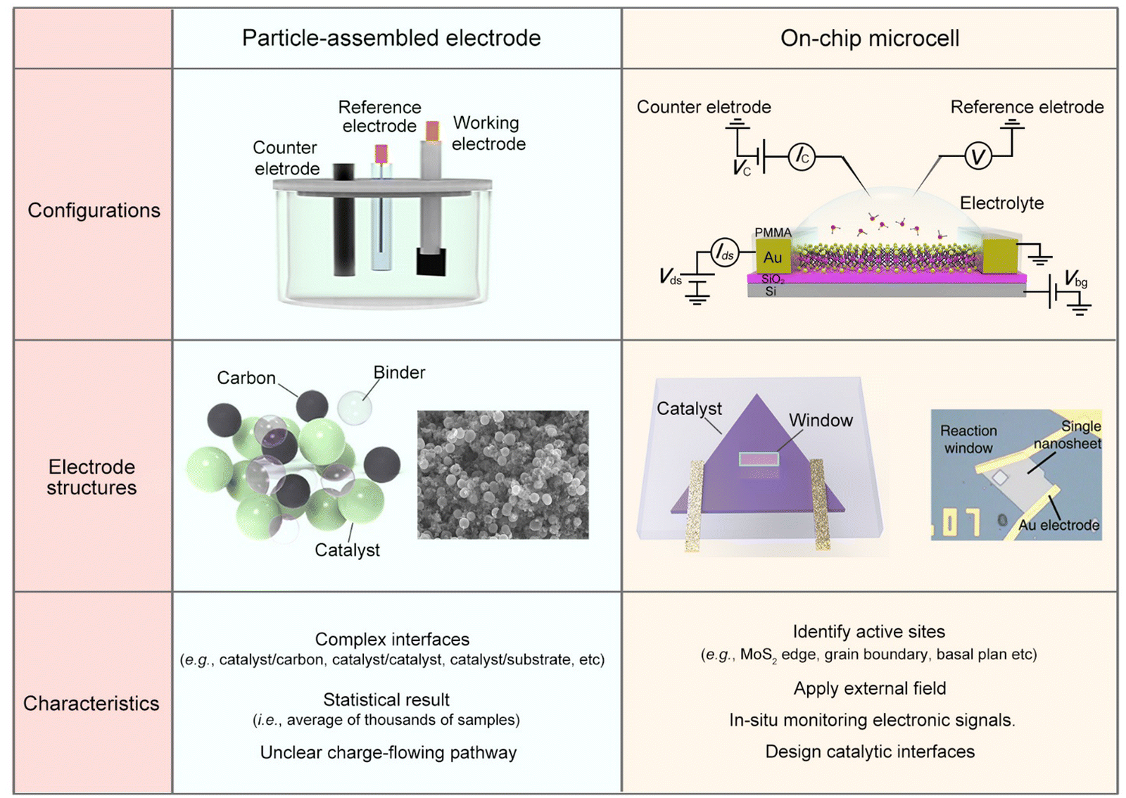 | ||
| Fig. 1 Comparison of the conventional particle-assembled electrode and on-chip microcell from three aspects: configurations, electrode structure, and characteristics. | ||
Along with advancements in micro-/nano-processing technology, an on-chip microcell has recently emerged and become a powerful tool in the electrocatalytic field to probe the catalytic behavior of the electrocatalyst at a single-catalyst level. Significant achievements have been made in such a field in the past nearly ten years, as shown in Fig. 2. For example, Mai et al. fabricated a single NW electrode device for in situ probing how electrode capacity faded in Li-ion-based energy storage devices, which is the first microcell example to study the correlation among material structure changes, transport properties, and electrochemical performance.18 Later, Ding et al. turned their attention to electrocatalysis and developed a four-electrode configuration that allows in situ monitoring of the surface adsorption/desorption features of metal NWs during the electrochemical process.19 Besides NW materials, the on-chip microcell was applied to two-dimensional (2D) NS materials. For example, Chowalla et al. constructed a low-resistance-contact microcell on monolayer MoS2 to compare the activity between the edge or basal plane.20 Similarly, Luo et al. set up microcell-combined in situ scanning time-resolved microscopy to spatially map the catalytic activity of monolayer MoS2 during the hydrogen evolution reaction (HER).21 Notably, such a cell that is derived from a semiconductor device is of particular interest in investigating the electronics-related behavior during the reaction process. For example, C. Frisbie et al. applied an electric-field modulation in an HER process.22,23 Moreover, using in situ electronic/electrochemical measurements, our group revealed a universal self-gating phenomenon to clarify the electronic-conduction modulation of >30 semiconducting catalysts during the electrocatalytic reaction.24 More recently, Duan et al. combined EIS and electrical transport spectroscopy (ETS) in a microcell to probe the behaviors of different cations (Li+, Na+, and K+) in HER kinetics.25
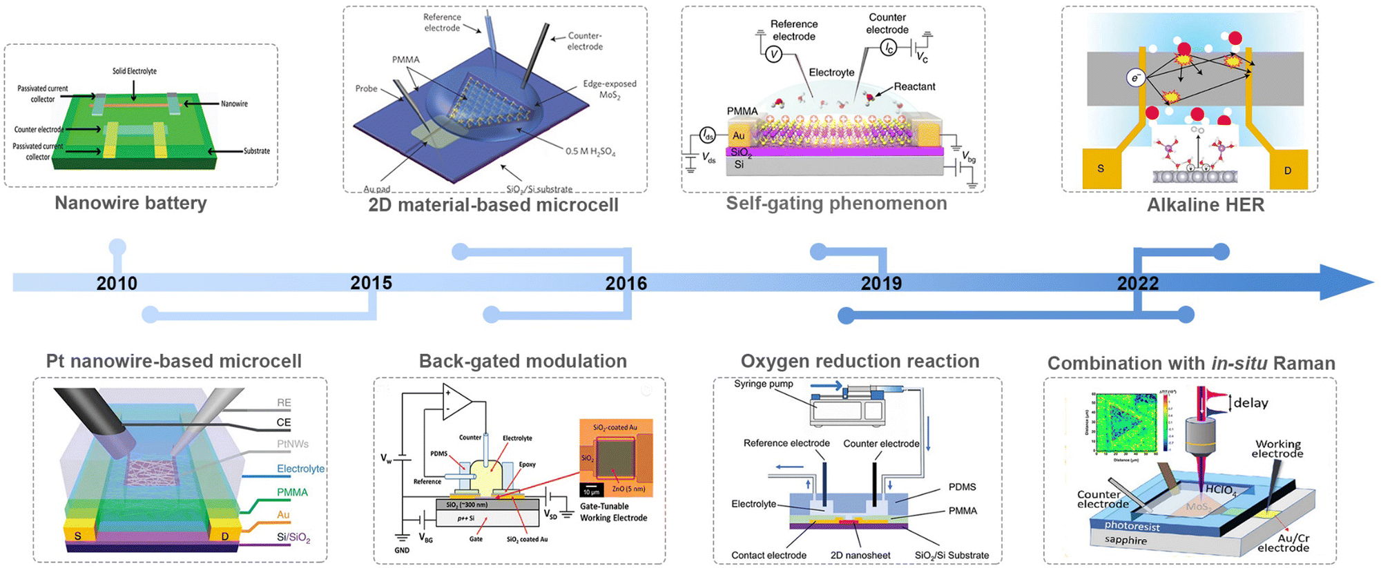 | ||
| Fig. 2 Development of the on-chip microcell in electrocatalysis. | ||
Based on those achievements, it is timely to provide a review on this field, hopefully attracting more attention for further development in model catalysis. Also, it is noteworthy that some excellent reviews have already been presented in this microcell field; unfortunately, there is still a lack of summaries paying much attention to its electronic characteristics, which is, essentially, derived from a semiconductor electronic device. In this review, we first discuss how the on-chip microcell was developed from an electronic device. Later, we will summarize current progress based on their two basic functions: one is to identify and monitor the active sites through the reaction-window function; the other one, from an electronic standpoint, is the circuit function, such as electrical field modulation, charge injection at the contacts, and in situ charge transport/transfer at metallic and semiconducting catalysts. Finally, we provide our perspectives on current challenges and implications in this emergent field.
2. Development of an on-chip microcell
This section will discuss how the on-chip microcells have been developed from the top-gated field effect transistors (FETs) and electric double-layer transistors (EDLTs). Both of them contributed to this microcell with well-defined device structures and mature micro-/nano-processing technology, playing a vital role in its emergence and broad applications in electrocatalysis. Given that FETs and EDLTs have been widely used in the electronic fields, while few are known in electrochemistry, their detailed working principles are also discussed in the following.The emergence of logic transistors in the 1940s dramatically accelerated the development of electronic devices and information systems. In particular, metal-oxide-semiconductor field effect transistors (MOSFETs) have been becoming the cornerstone in those fields.26–28Fig. 3a shows the device structure of a typical MOSFET (Fig. 3a), in which the gate voltage is applied through a top electrode, electrostatically tuning the distribution of the charge carriers at the oxide-semiconductor interface.29–31 The type and density of the charge carriers can be determined by the sign and magnitude of the voltage applied at the top gate, respectively. As a result, the gate voltage continuously controls the semiconductor's conductance, realizing the smooth switch between “on” and “off” states. Note that, owing to a low dielectric constant of traditional oxides (e.g., ∼10−2 μF cm−2 for 300 nm SiO2),32 a large gate voltage is usually needed to realize the above state switch, for example, 10–100 V for the MOSFET based on carbon nanomaterials and metal oxides.33
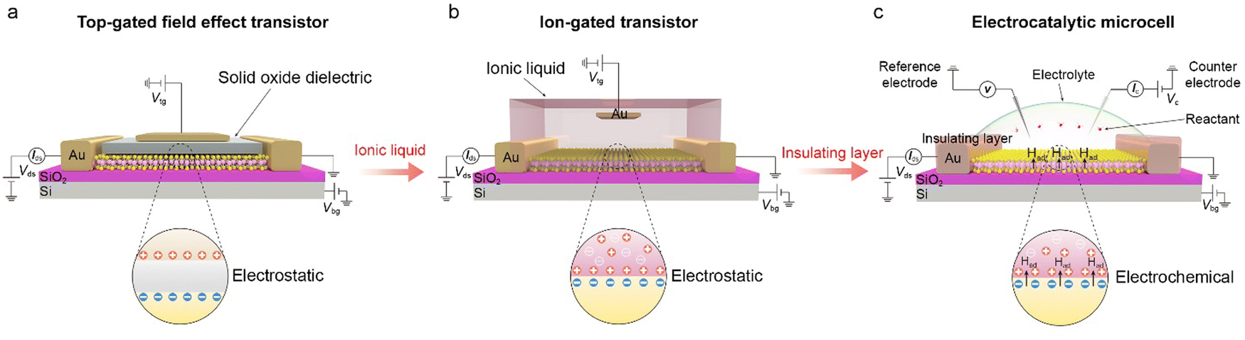 | ||
| Fig. 3 Evolution of the on-chip electrocatalytic microcell. (a) Schematic illustration of the top-gated field effect transistor (FET). It is based on a metal–insulator–semiconductor junction, in which the insulator adopts the solid oxide (grey region). When the positive voltage is applied at the top gate (brown region), the negative charge carriers could be induced and accumulate at the oxide-semiconductor interface (grey-yellow region). The carrier concentration depends on the capacitance of the solid oxide and applied voltage. (b) Schematic illustration of the ion-gated transistor, that is, the electric double-layer transistor (EDLT). By changing the solid oxide insulators with a high-mobility ionic liquid, an electric double-layer is formed at the interface, serving as a nanogap parallel plate capacitor with a substantial capacitance (up to 100 μF cm−2). As a result, applying a low voltage (e.g., 0.1–0.5 V) can achieve high carrier densities (e.g., beyond 1015 cm−2), showing more efficiency of conductance modulation. (c) Schematic illustration of the electrocatalytic microcell. Based on the above EDLT structure, the on-chip microcell has been developed by replacing the ionic liquid with reactive electrolytes (e.g., H2SO4, HClO4, phosphate buffer saline, and KOH2) and introducing an insulating layer (such as PMMA, photoresist, or SiO2 films) to make the reaction windows. The counter and the reference electrode are also used to normalize the reaction voltage to the standard electrochemical potential. Regarding those developments, such a cell exhibits two basic functions: reaction window and circuit, corresponding to an electrochemical view as well as an electronic view, respectively. | ||
In the 1980s, EDLTs34,35 that employed an ionic liquid to replace the conventional oxide dielectric were proposed, as illustrated in Fig. 3b. In an EDLT, the applied top-gate voltage (positive) drives the cations toward the semiconductor interface to form an electric double layer (EDL), which can electrostatically modulate the charge carriers of the semiconductor channel.36,37 Such an EDL can be regarded as a nanogap parallel plate capacitor with a capacitance of up to 100 μF cm−2, much larger than that in MOSFETs.35 Such a giant capacitance can achieve an ultrahigh carrier accumulation beyond 1015 cm−2 at just several volts, resulting in more effective modulation of charge carriers compared to the above MOSFETs.38,39 Moreover, such an EDLT has also come out with a new interdisciplinary concept, i.e., iontronics. This bridges electronics and ionics, with broad applications in electrochemistry, solid-state physics, electronic engineering, and biological sciences.36 For example, Iwasa and colleagues achieved the insulator-metal transition of VO2 film by applying just one voltage through EDLTs.40
More recently, through introducing an insulating layer and changing the ionic liquid into catalytically-active electrolytes, such as H2SO4,20,41,42 KOH,25,43,44etc., those above EDLTs can be transformed into an on-chip microcell used in the electrocatalytic field (Fig. 3c). One of the most significant advancements is that the introduced insulating layer, e.g., PMMA or SiO2, allows one to selectively expose the region of interest through a window fabricated by the micro-/nano-processing technology, such as e-beam lithography (EBL), for a given reaction. Such a window enables various electrocatalytic reactions to only occur in the region of interest and obliviate the leakage current from the metal electrodes. Benefiting from the reaction window, the precise micro-area measurement is achievable through the on-chip microcell, which helps to investigate the active sites in electrocatalysis.
Following the above timeline, two points need to be noted here for comparing on-chip microcells with the above electronic transistors, as follows:
One is the leakage current generated from the gating electrode in the electronic transistors. As is well-known, it must be avoided; on the contrary, such a current is needed for the on-chip microcell, which corresponds to the signal of the catalytic reaction (i.e., the charge transfer process). Taking the HER process as an example, the leakage collected in a microcell is that the reactants (H3O+) receive the electrons at the active sites and generate the adsorbed hydrogen atoms (Had).45
The other one is conductance modulation arising from EDL. The EDL widely exists in both EDLT and on-chip microcells; in the former, EDL can effectively modulate the conduction of the channel. Similarly, in the latter, it can also modulate the nonmetallic catalysts (conductive or even insulated). Therefore, an in situ conductance evaluation should be performed in on-chip microcells to verify whether the microcell works during the measurements. However, such an evaluation is usually neglected in the current microcell measurement.
3. Fabrications and characteristics of on-chip microcells
Fig. 4 shows the typical fabrication procedures of on-chip microcells, with 2D TMD material as an example. First, a 16 mm × 16 mm SiO2 (285 nm)/Si chip with pre-patterned 32 or 16 Au contact pads was fabricated using conventional photolithography followed by thermal evaporation. Second, CVD-grown or mechanically exfoliated 2D catalysts were transferred onto the chip. Subsequently, an EBL process, followed by thermal evaporation, was used to fabricate the drain and source metal contacts (Cr/Au or Ti/Au). Finally, the whole chip was passivated by 1 μm-thick PMMA film, and a second EBL process was adopted to carve windows on the catalytic region. As a result, spatial control of the electrocatalytic reaction was achieved through such a PMMA-passivated window, which ensured that the reaction only occurred in the region of interest.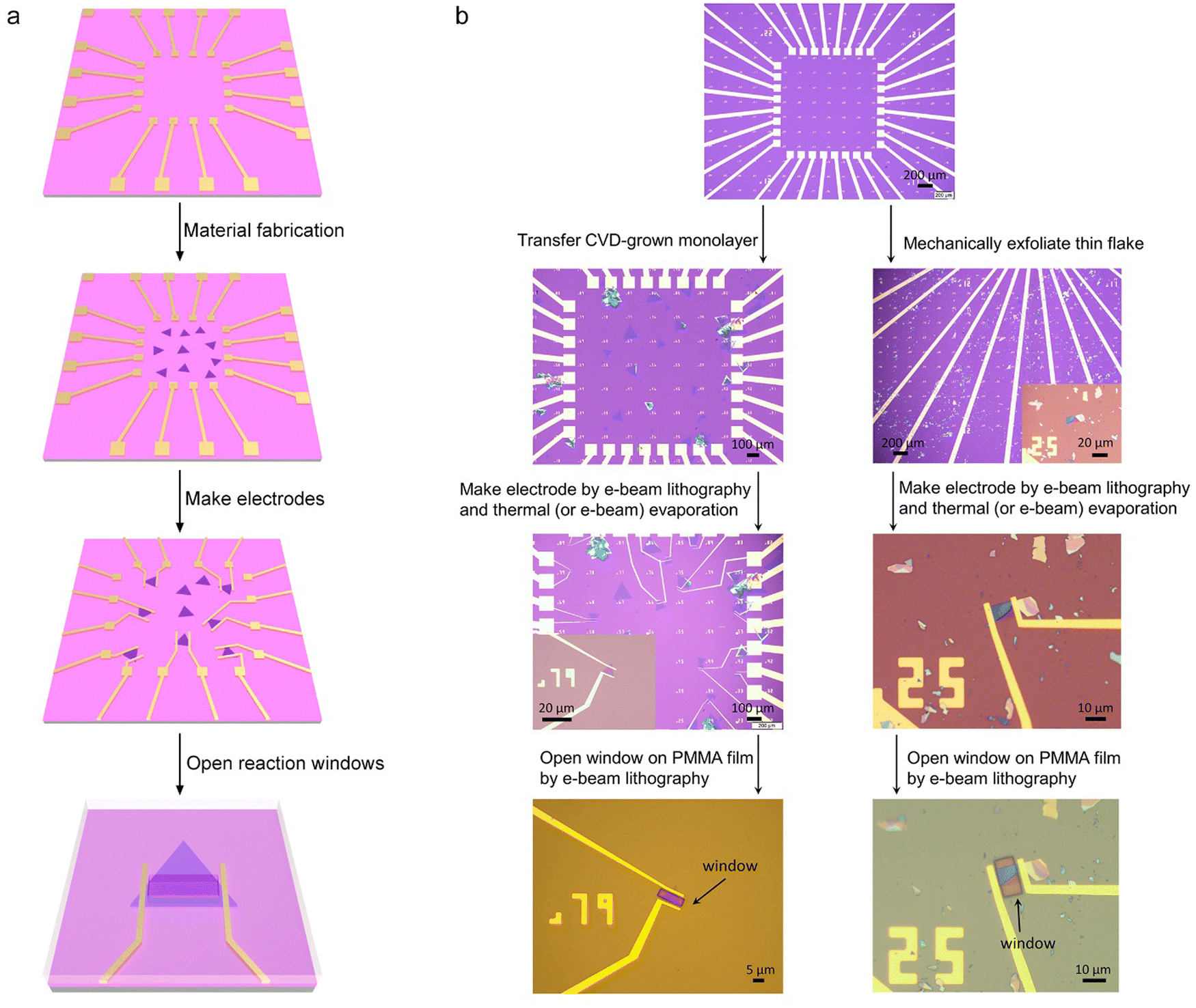 | ||
| Fig. 4 Fabrication process of an on-chip microcell. (a) Schematic illustration of the fabrication steps of the on-chip microcell. (b) Typical fabrication procedures in 2D TMD-based microcells, in which CVD-grown and mechanically-exfoliated samples were introduced, respectively. | ||
Currently, the signals collected from the on-chip microcells are usually several or tens of nA, thus putting forward a high precision requirement for the electrochemical workstation. For example, to obtain a smooth Tafel slop in the HER, the background noise current should be kept as low as 10−11 A. Alternatively, high-precision source measurement units (SMUs) could also be used to meet such a requirement. Here, we took an in situ electronic/electrochemical measurement in our lab as an example for a detailed introduction; please see the testing environment and setup in Fig. 5. First, four electrodes were used, including microcell graphite and an Ag/AgCl micro-reference as the counter and reference, and the other two electrodes as the working electrodes connected to the catalysts (as the source and drain contacts to collect the in situ electronic signals during the electrocatalysis). Second, in our setups, two source measurement units (SMU), i.e., SMU 1 (Keithley 2400) and SMU 2 (Keithley 2450), were used instead of traditional electrochemical workstations. Their equivalent circuit diagram is presented in Fig. 5. In SMU 1, the “High Force (Force HI)” and “Low Force (Force LO)” are connected to the source and drain electrodes on the catalyst for the electronic measurement (Ids). In SMU 2, both “Low Force (Force LO)” and “Low Sense (Sense LO)” terminals are connected with the working electrode, and the “High Force (Force HI)” and “High Sense (Sense HI)” terminals were connected to the counter electrode and reference electrode for the electrochemical measurement (Ic). These two measurements are synchronized by the general-purpose interface bus (GPIB) and the Labview script, allowing simultaneous recording of the electronic and the electrochemical signals.
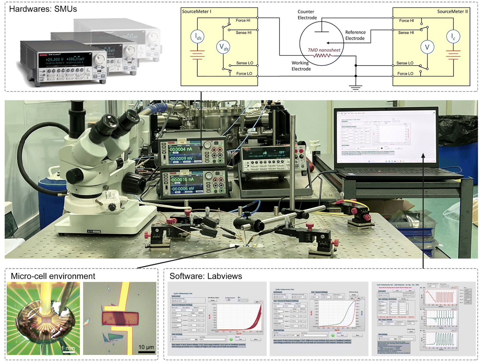 | ||
| Fig. 5 The typical testing setups used in our lab. The hardwares involved in the test are source measurement units (SMUs), and the software is Labview. Taking in situ electronic/electrochemical measurement as an example, SMU 1 and SMU 2 are used for the electronic and the three-electrode electrochemical measurements, respectively, as the equivalent circuit diagram shows. | ||
Taking the above advantages, such an on-chip microcell presents several fantastic features (see Fig. 1), including (i) identifying the active sites through reaction windows. Such a window is able to expose regions of interest on a catalyst using an insulation layer (such as PMMA); (ii) regulation of the reaction through applying an external electrical field. Based on a field-effect-transistor circuit, such a microcell also enables regulating the electrochemical reaction, e.g., activity or interface, by applying an electrical field using a back gate voltage; (iii) in situ monitoring electronic signals. Derived from a semiconductor electronic device, such a cell can in situ probe the conductance of the catalyst during a reaction process. Finally, (iv) design of the catalyst interface. Using the micro-/nano-processing technology, various heterostructure interfaces, such as bottom-/top-electrodes, and interfinger electrodes, could be designed. Thanks to those features, several interesting functions have been derived, contributing to an extensive development of microcells in electrocatalysis, which will be discussed in the following.
4. Functions of on-chip microcells
In this section, we will discuss current achievements on on-chip microcells through paying attention to their two basic functions: the reaction window and the circuit. The reason why we made such a classification is based on the interdisciplinary behavior of on-chip microcells, that is, the combination of electrochemistry and electronics. On the one hand, with the assistance of the reaction window, microcells can be used to study the active sites, such as identifying what they are as well as monitoring how they change. On the other hand, derived from the FET or EDLT circuits, they enable investigating the reactions from an electronic point of view, such as external electrical field modulation, contact engineering for charge injection, and in situ conductance measurement of metallic and nonmetallic catalysts.4.1 Reaction window
In an on-chip microcell, the reaction window is carved by EBL on a PMMA-covering layer, capable of exposing regions of interest at a micro-size for a given electrocatalytic reaction. Thanks to such a window, this cell provides a promising platform to identify the active sites and monitor their changes at a single-material level, which is crucial for the rational design of excellent catalysts as well as the exploration of the mechanism behind the reaction.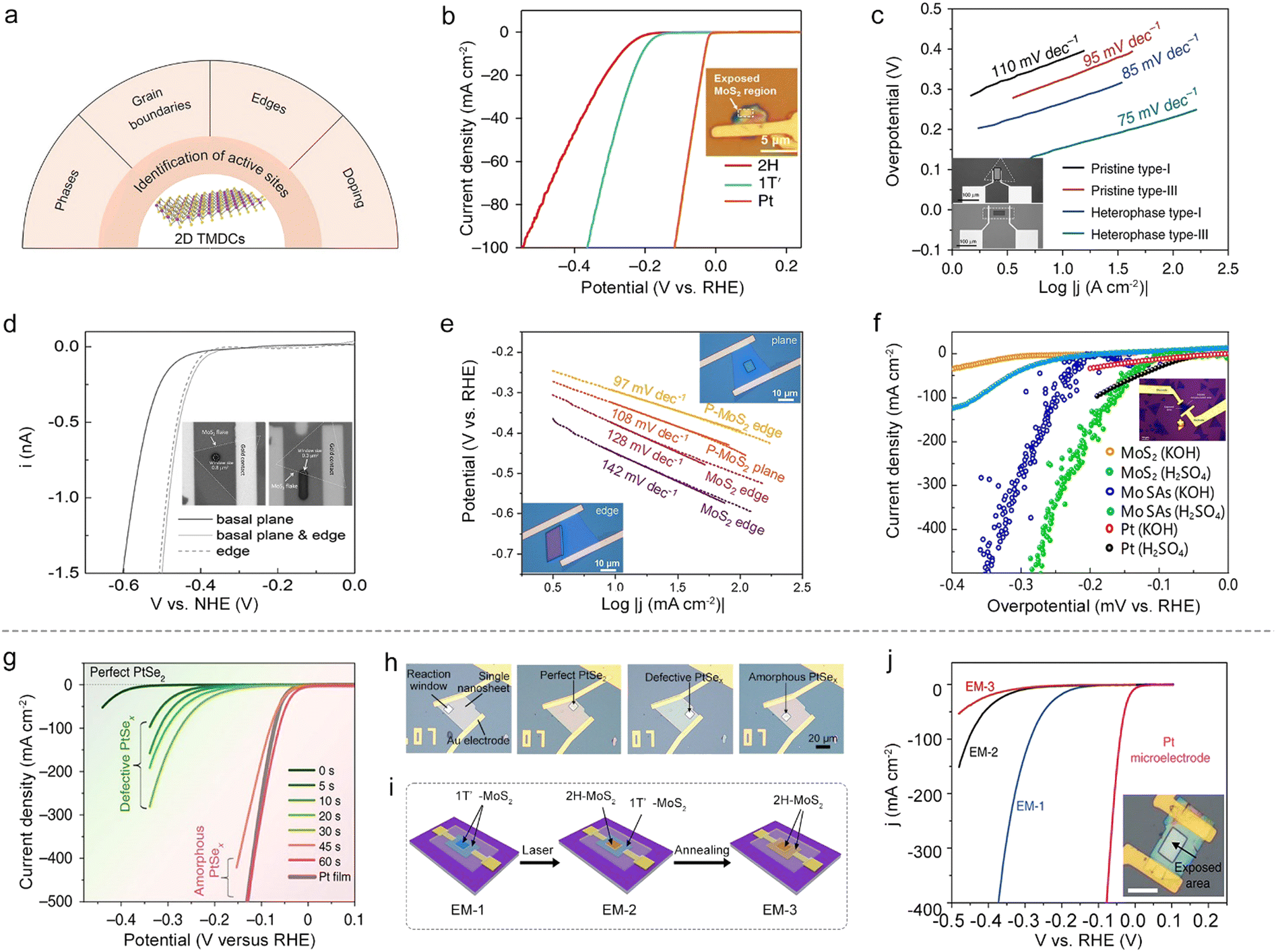 | ||
Fig. 6 Identifying active sites and monitoring their changes at a single material. (a) Various active sites for 2D TMDCs identified by on-chip microcells. (b) Polarization curves of Pt, 1T′-MoS2 and 2H-MoS2. Inset: The optical image of the microcell. (c) Tafel plots of MoS2 with different types of domain boundaries. Inset: The optical images corresponding to the single-crystal MoS2 microcell without 2H–2H domain boundaries and the polycrystalline MoS2 microcell with domain boundaries. (d) Polarization curves of the MoS2 basal plane with and without edge active sites. Inset: The optical images of MoS2 microcells with exposed edges and basal planes. (e) Tafel plots of the basal plane and edge sites. Inset: The optical images of a P-MoS2 microcell with exposure of the edge and the basal plane. (f) Polarization curves of MoS2, Mo SAs sitting on cogenetic MoS2 (Mo SAs/ML-MoS2) and Pt. Inset: The optical image of the microcell. (g) Polarization curves of the PtSex NS with a 0 to 60![[thin space (1/6-em)]](https://www.rsc.org/images/entities/char_2009.gif) s treatment duration. (h) Optical images of PtSex microelectrodes with reaction windows through different plasma treatment times. (i) Schematic of the fabrication of three types of electrochemical microcells (EM-1, EM-2, and EM-3) via a phase-transition strategy. (j) Polarization curves of EM-1, EM-2 and EM-3. Inset: The corresponding optical image of EM-1. s treatment duration. (h) Optical images of PtSex microelectrodes with reaction windows through different plasma treatment times. (i) Schematic of the fabrication of three types of electrochemical microcells (EM-1, EM-2, and EM-3) via a phase-transition strategy. (j) Polarization curves of EM-1, EM-2 and EM-3. Inset: The corresponding optical image of EM-1. | ||
Phases. The phases have a profound effect on the catalytic properties and the conductivity for 2D TMDCs. For example, 2H-phase MoS2 is relatively stable while electrochemically-inert; on the contrary, its 1T-phase or 1T′-phase counterpart present metallic behavior with a better HER activity.55,56 However, since they usually mix in a sample, it is challenging for the conventional particle-assembled electrodes to distinguish the intrinsic activity of each phase. Aiming at solving this issue, Jiao and co-workers synthesized a 1T′-MoS2 monolayer with high purity and crystallinity through a potassium (K)-assisted chemical vapor deposition (CVD) method, and then compared its activity with the 2H-phase counterpart using a microcell. It can be seen from Fig. 6b that 1T′-MoS2 exhibits higher catalytic performance than its counterpart, which is attributed to the efficient electrical coupling between the substrate, rapid electron transport, and increased catalytic active sites as well.57
GBs. As one of the line defects, GBs are universally found in 2D materials. Using the on-chip microcell, the activity of a single GB can also be detectable. For example, Liu and co-workers compared the HER activity among a single GB, a single edge and the basal plane.48 The results showed that the GB had better activity than the edge and basal plane. To further make use of such a GB site, the authors demonstrated the synthesis of wafer-size TMD films with an ultra-high density of GBs (up to 1012 cm−2). Those films showed an excellent hydrogen evolution performance (onset overpotential, ηonset: 25 mV and Tafel slope: 54 mV dec−1), thus indicating an intrinsically high activation of the TMDC basal plane.
On the other hand, besides the above homo-phase ones, homo-phase GBs can also be fabricated using phase engineering, whose improved activity could be verified by microcells. For instance, Zhang and co-workers utilized an on-chip microcell to investigate the HER activity between 2H–2H homo-phase and 2H–1T hetero-phase ones in MoS2, as shown in Fig. 6c. Compared with pristine type-I and type III samples (2H–2H homo-phase GBs), an improved catalytic performance was observed in the 2H–1T hetero-phase, which is ascribed to the metallic 1T-phase offering better charge transport capacity than the 2H-phase.58 Alternatively, Yang et al. recently studied the activity of hetero-phase GBs between the 2H-phase and 1T′-phase in MoTe2 films. The microcell measurement showed a clear improvement of HER activity for 2H–1T′ hetero-phase GBs compared with the pristine MoTe2. This is the result of their local electronic structure and their unique covalent nature.49
Edges. The edges of 2D TMDCs with an unsaturated coordination environment are usually electrochemically active. For example, through the selective exposure of the edge in an on-chip microcell, Lou and co-workers have examined its HER activity in 2H and 1T′-MoS2 monolayers. Moreover, the linear sweep voltammetry (LSV) curves in Fig. 6d showed that the edge gave a much higher HER activity than that of the basal plane.50 Beyond the MoS2 catalyst, the microcell is also applicable for identifying the activity of edge sites for other 2D materials, such as WTe2 and PtSe2. For instance, Cha et al. investigated the activity of (010) and (100) edges of WTe2 in an on-chip microcell. The results demonstrated that the (100) edge was more active, which could be correlated to its lower Gibbs free energies of hydrogen adsorption (ΔGH*) than that of the (010) edge.59 Subsequently, Jiao et al. probed the HER activity of the PtSe2 edge by using a microcell to expose the edge and basal plane selectively. The edge also showed much higher catalytic performance, similar to the above examples of 2D MoS2 and WTe2.51
Doped atoms. Owing to the abundant valence states and flexible oxidation capabilities, doping atoms, such as B,60 F,61 N,62 P,54,63 and Mo,64 can also enhance the HER activity of 2D materials. More recently, Ye et al. studied the edge effect of phosphorus (P) doping on a MoS2 NS (Fig. 6e). The Tafel curves indicated that the P-MoS2 edge had the lowest Tafel slope among those samples, as a result of its lower hydrogen adsorption energy and hydrogen evolution activation barrier.54 Apart from nonmetal doping of TMDCs, metal doping has also been extensively studied to activate the basal plane of TMDCs. For example, Liu and co-workers utilized a cold hydrogen plasma reduction method to synthesize Mo-single-atom doped MoS2, as shown in Fig. 6f. The microcell measurements show that such a catalyst shows more exceptional intrinsic activity with an overpotential of 261 mV and 209 mV at 10 mA cm−2 in 0.5 M H2SO4 and 1.0 M KOH, respectively. The authors claimed that the improved performance is a consequence of the increase of the bond strength through hybridization, leading to fast hydrogen adsorption/desorption kinetics and superior hydrogen evolution activity.64
A typical example is that Liu et al. adopted plasma treatment to obtain desired regions, e.g., perfect single-crystal, defective single-crystal, and amorphous PtSex on a single PtSe2 NS, for a fair comparison among their HER activities. Fig. 6h shows the optical images of those microelectrodes with different reaction windows, and the electrocatalytic performances of these regions are summarized in Fig. 6g. It is worth mentioning that an abruptly improved performance was observed in the microcell, solely corresponding to the transition of the catalytic site during this etching process, that is, from Se vacancies to the amorphous Pt sites. Such a finding gave direct evidence of how the active sites changed during the etching process.10 Similarly, Zhai and co-workers precisely controlled the oxidation degree at a single MoTe2 NS by the varying processing times with O2 plasma. Using an on-chip microcell, they carefully monitored the changes of active sites under defect engineering. The experimental results first verified a high onset overpotential of 280 mV for the pristine MoTe2 NS, showing a nearly HER-inert activity. Impressively, as the O2-plasma treatment time extended, a linear decrease of the onset overpotential of the oxidized MoTe2 was observed, and such a linear behavior was solely ascribed to the oxygen vacancies that increased the surface charge and reduced ΔGH*.65
Besides the above factors, the TMDC thickness can also affect the catalytic properties, which the on-chip microcell could precisely monitor. For example, Jiao et al. studied the influence of PtSe2 thickness on the HER activity at a single NS using the on-chip microcell. In the experiment, the authors firstly made a single-crystalline 2D PtSe2 NS with a controlled number of layers, and then probed the HER activity at the thickness-varied regions through the reaction window. Note that, such a measurement allowed a precise evaluation of the activity change only originating from the thickness effect. Finally, in conjunction with theoretical calculations, they clearly demonstrated how the number of layers affected the active sites of 2D PtSe2 NSs and correspondingly altered their HER performances.51
Beyond a sole factor, the on-chip microcell can further monitor multiple factors affecting the catalytic reaction. A typical example is that Zhang and co-workers conducted phase-dependent HER studies in electrochemical microcells. In their experiment, they constructed a microcell based on a highly-crystalline 1T′-phase MoS2 NS, enabling monitoring of the activity changes step-by-step during the phase-transformed process for a fair comparison (Fig. 6i). First, keeping the contact unchanged, they showed that the basal plane 1T′-MoS2 (EM-1) was much more active than its 2H counterparts (EM-2), which could only be attributed to its higher intrinsic activity. Second, keeping the exposed region unchanged, they demonstrated that the 1T′-metallic-phase contact (EM-2) showed a better charge-injection capability than the 2H-semiconducting-MoS2 (EM-3), contributing to a high HER performance (Fig. 6j). Together, those results that were obtained by the on-chip microcells provided a unique opportunity to study the effect on electrocatalysis solely based on the crystal phase.66
4.2 Circuits
Besides the reaction window's function, the other one is the circuit of the on-chip microcell that stems from the FET or EDLT behavior. It provides a great platform to modulate and monitor the reaction processes with an electronic point of view, such as external electrical field modulation,67–69 charge injection,59 and in situ interface charge translation monitoring.44,70,71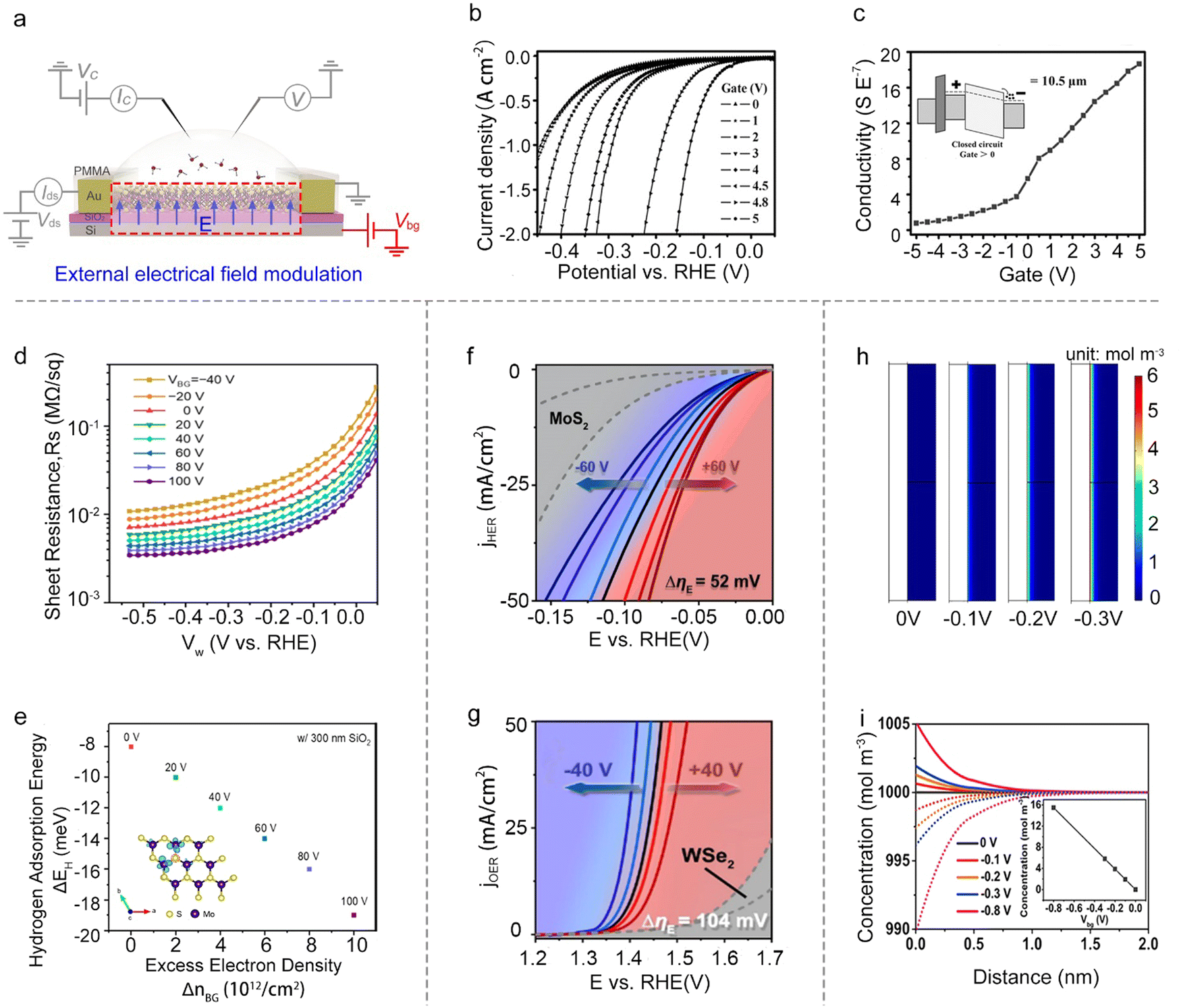 | ||
| Fig. 7 External electrical field modulation. (a) Schematic illustration of the external field electrical modulation principle via a microcell. (b) The polarization curves of the HER at different back-gate voltages. (c) The channel conductance of the MoS2 NS changed with gate voltage observed in a microcell. Inset: The energy band of MoS2 at the positive gate voltage bias (the inset image). (d) Sheet conductance (Rs) at different back gate voltages (VBG) in 0.5 M H2SO4 (the source-to-drain bias is 5 mV). (e) Computed hydrogen adsorption energies (ΔEH) as a function of excess electron density (ΔnBG). Inset: The charge-density map of monolayer MoS2 with 5.5% S vacancies at a VBG of +100 V. (f) The HER polarization curves of Pt SAs/MoS2 at different back gate voltages. (g) The OER polarization curves of Co SAs/WSe2 at different back gate voltages. (h) The simulation of the stationary state of net charge distribution in the interface of the electrolyte and catalyst induced by additional bias. (i) Redistribution of H+ (line), SO42− (dots), and net charge (inset) induced by different back gate voltages. | ||
Besides, the electric field can also modulate ΔGH*. For example, Frisbie et al. demonstrated an enhanced HER performance when increasing the back-gate voltages from −40 V to 100 V on MoS2 devices. Notably, they didn’t observe an evident decrease in the sheet resistance of the monolayer MoS2, thus excluding the possible influence raised from the conductivity discussed above. Furthermore, their density functional theory (DFT) calculations showed that the gate-induced charging of the localized Mo d-states at the active (S-vacancy) sites would increase the Mo–H binding energy. Combined with theory and experiments, they claimed that the increase in HER activity is due to the increased intrinsic reactivity of the active sites in monolayer MoS2 under a positive gate voltage.78 A similar phenomenon was observed by other researchers.79,80 Dong et al. demonstrated that the ΔGH* of electron-dominated WSe2 is much lower than that of hole-dominated WSe2 under the electrical field modulation. Furthermore, Zhai et al. revealed the fact that the external field finely modulated the intermolecular charge transfer of the cobalt phthalocyanine (CoPc)/MoS2 heterojunction and enhanced the Mo–H bonding.
Moreover, turning attention to the single-atom catalysts (SACs), Ding et al. reported the manipulation of local catalytic sites of single-atom catalysts anchored on 2D atomic crystals via a precisely controlled external electric field. Using the microcell, a series of model SACs have been systematically studied, such as Pt single atoms (SAs) and Co SAs on n-type MoS2, p-type WSe2, and metallic graphene. Specifically, the Pt SAs on n-type MoS2 demonstrate significant improvement in HER activity under positive external electric fields (Fig. 7g), and the Co SAs on p-type WSe2 achieved a dramatically-enhanced activity for the oxygen evolution reaction (OER) under negative ones (Fig. 7f). Combined with theoretical calculations, they attributed such electric field-induced performance enhancement to “onsite electrostatic polarization” in their SAC systems, where the electric field markedly influences the charge redistribution of SACs, leading to the optimization of the chemical bonding between SA and key adsorbates, the spatial distribution of outward charges, and the reaction kinetics of the rate determining steps as well.81
The external electrical field can also tune the distribution of the ions at the electrolyte-catalyst interface. For example, Mai et al. used the pristine VSe2 NS as the catalyst and studied the distribution of the ions at the electrolyte-VSe2 NS interface under varied back gate voltages. Using COMSOL simulation, they demonstrated that the back gate voltage would induce the redistribution of the ions at the interface (Fig. 7h); that is, the H+ preferred to concentrate on the surface (Fig. 7i). Such a redistribution would realize the enhanced electron transport process, and thus facilitate the rate-limiting step under the HER process. As a result, they achieved a low onset overpotential at 10 mA cm−2 (η10 = 70 mV) in VSe2 NSs without any chemical treatment.82 Overall, the external field effect is a powerful strategy to regulate the catalytic reactions; however, the above factors (e.g., conductivity, intrinsic activity, and ion redistribution) would usually interfere with each other, complicating the mechanism analysis for a given reaction.
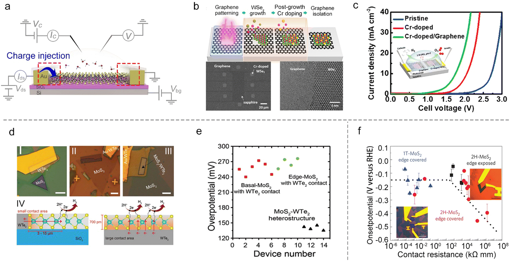 | ||
| Fig. 8 Contact engineering for charge injection. (a) Schematic illustration of the charge injection principle via a microcell. (b) Schematic of the formation process of the Cr–WSe2/graphene heterojunction. (c) Polarization curves of the overall water splitting of Cr–WSe2/graphene and the corresponding microcell shown in the inset image. (d) Optical images of three types of WTe2–MoS2 heterostructures with WTe2 contact (I, II, and III) and the charge injection pathways of WTe2 edge-contact and heterostructure-contact. (e) The corresponding overpotentials of three types of heterostructures in (d). (f) The influence of the contact resistance on the HER onset potential of MoS2. Inset: The optical images of single-layer MoS2 microcells with exposure of the edge (left) and the basal plane (right). | ||
In heterostructures, graphene with high conductivity85 and an atomically-flat behavior,86 is a promising substrate to facilitate charge injection into the semiconductor materials. Such a strategy has already been widely adopted in TMD-based semiconductor devices.87,88 For example, Cha et al. showed that the HER activity of MoS2 could be improved by introducing a graphene-supporting layer to form a MoS2/graphene heterostructure.59 Similarly, Chen et al. used a stitching contact process to directly grow the bifunctional Cr-doped WSe2/graphene for overall water splitting, as shown in Fig. 8b. They constructed a microcell based on such a heterostructure for overall water splitting (the inset of Fig. 8c), and it shows a much-lowered overpotential (a reduction of 980 mV at 10 mA cm−2) under neutral conditions as compared to that of the pristine WSe2 microcell with gold metal contact. The authors attributed such a superior performance to the self-stitching heterojunction with a lower contact resistance.89 Besides the above graphene contact, Cha et al. also constructed a WTe2–MoS2 microcell with a WTe2 metallic contact. As shown in Fig. 8d, they systematically investigated the basal plane (I) and the edge (II) in single-layer MoS2 and the basal plane in the MoS2–WTe2 heterostructure (III) using the microcells. It turns out that type III obtained the most outstanding property with the lowest overpotential (135 mV ± 5 mV) compared to the other two types (255 mV ± 15 mV), as shown in Fig. 8e. The authors attributed such an enhancement of HER activity to the increased contact area that enhanced the charge injection to the catalyst site in the MoS2–WTe2 heterostructure (Fig. 8d IV).90
Besides the heterostructure, phase transition engineering has been used to lower the contact resistance to enhance the charge injection.91 For example, Chowalla et al. first used phase transition engineering to provide insights into the role of electronic coupling between the substrate and MoS2 NS.20 In that work, the authors made the microcells based on monolayer MoS2, and used n-butyllithium to convert the 2H-phase contact into a metallic 1T-phase one (that is, phase-engineered contact). The HER catalytic properties of the basal and edge plane of MoS2 were examined, respectively, as shown in Fig. 8f. They demonstrated that phase-engineered low-resistance contact facilitated the charge injection from the substrate to the catalysts, making the activity of the 2H basal plane (having S vacancies) comparable with 1T-phase and edge-exposed microcells (Fig. 8f). As a result, the authors claimed that the contact resistance is an essential factor, which must be evaluated when comparing the relative activities among different types of MoS2 catalysts for the HER.
Semiconducting catalysts. As discussed in Section 2, an EDL-induced giant capacitance exists at the interface, which could achieve an ultrahigh carrier accumulation (1015 cm−2 at just several volts). Such a characteristic will lead to an effective conductance modulation for semiconducting catalysts, as shown in Fig. 9a. Fortunately, the on-chip microcell allows one to in situ observe this conductance modulation and analyze the corresponding mechanism. For example, our group observed that the electrocatalytic reaction itself could strongly modulate the surface conductance of semiconductor electrocatalysts, and such a phenomenon was defined as self-gating. Fig. 9d–f shows the typical in situ electronic/electrochemical measurements of n-type, p-type, and bipolar semiconductors during electrocatalysis, respectively. The semiconducting catalysts can be modulated to be highly conductive (“on”) or insulating (“off”), strongly correlating with the electrocatalytic reactions, that is, n-type semiconductor catalysts (e.g., MX2; M = Mo, W, Re; X = S, Se) favor cathodic reactions such as the HER, p-type ones (e.g., Ni and Co-based catalysts) prefer anodic reactions such as the OER, and bipolar ones (e.g., Ta/Nb-doped MoS2 or WS2) tend to perform both anodic and cathodic reactions.93
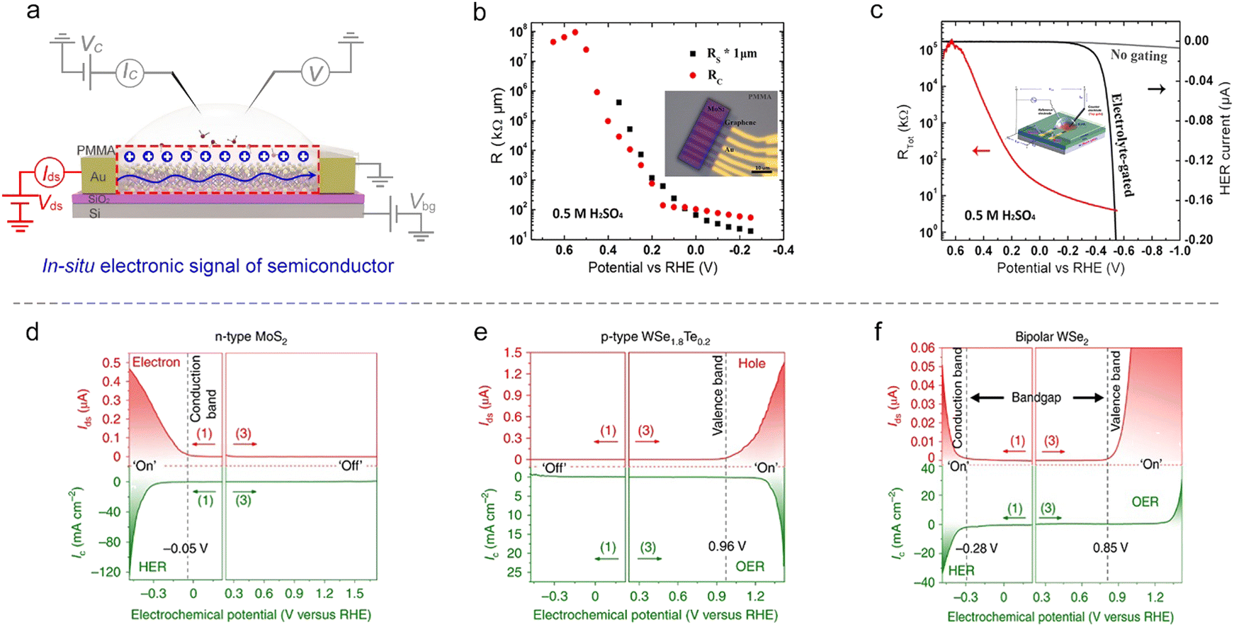 | ||
| Fig. 9 In situ conductance measurement on semiconductor NSs. (a) Schematic illustration of the microcell-based in situ electronic/electrochemical measurement. (b) The MoS2 sheet conductance (Rs) and MoS2/graphene device contact resistance (Rc) recorded at different applied potentials, obtained from transfer length method (TLM) measurements. Inset: The top view of the image of the TLM platform based on a rectangle-patterned monolayer MoS2 with a graphene bottom-contact. (c) Real-time total resistance (Rtot) curve (red) recorded along with the HER LSV curve (black) in 0.5 M H2SO4. Inset: The device with a channel length of 1 μm. The LSV measurement was carried out at 20 mV. The gray curve shows a simulated iR-uncorrected HER LSV, which is extracted from the measured data (the black curve). (d)–(f) Demonstration of the self-gating phenomenon by in situ electronic/electrochemical measurement on n-type MoS2 (d), p-type WSe1.8Te0.2 (e), and bipolar WSe2 (f). In (d), n-type MoS2 is turned on at a negative electrochemical potential and delivers the HER. In (e), p-type WSe1.8Te0.2 is turned on at a positive electrochemical potential and delivers the OER. In (f), bipolar WSe2 is turned on at both negative and positive electrochemical potentials and can deliver the HER and OER. | ||
Close to the time of the above work, Esposito et al. observed a similar phenomenon. In combination with the transfer length method (TLM) and microcell, they first investigated the MoS2 sheet resistance in the electrochemical environment. They found that both its sheet resistance (Rs) and contact resistance (Rc) decreased with the applied potential (Fig. 9b). To correlate with the HER process, they next in situ recorded the polarization current and the total resistance (Rtot) of MoS2 simultaneously at varied HER potentials. They observed a significant decrease (up to 5 orders of magnitude) of the Rs with the HER potential, thus demonstrating a similar gating phenomenon (Fig. 9c). The authors also demonstrated that the gating efficiency is strongly dependent on the electrode configuration, where the MoS2 layer was positioned between the electrolyte and the back contact can realize the full benefits of such a gating effect.94
Metallic catalysts. The conductance of metallic nanostructures would also be affected under EDL, because the surface-bound molecules would scatter their electron density.71 Such an effect will be magnified as the size of nanostructures is reduced to several nanometers, e.g., ultrafine metallic NWs. Therefore, in situ monitoring of the metallic nanostructures’ conductance also presents a potential method to study ion adsorption/desorption behavior during the reaction process, as shown in Fig. 10a.
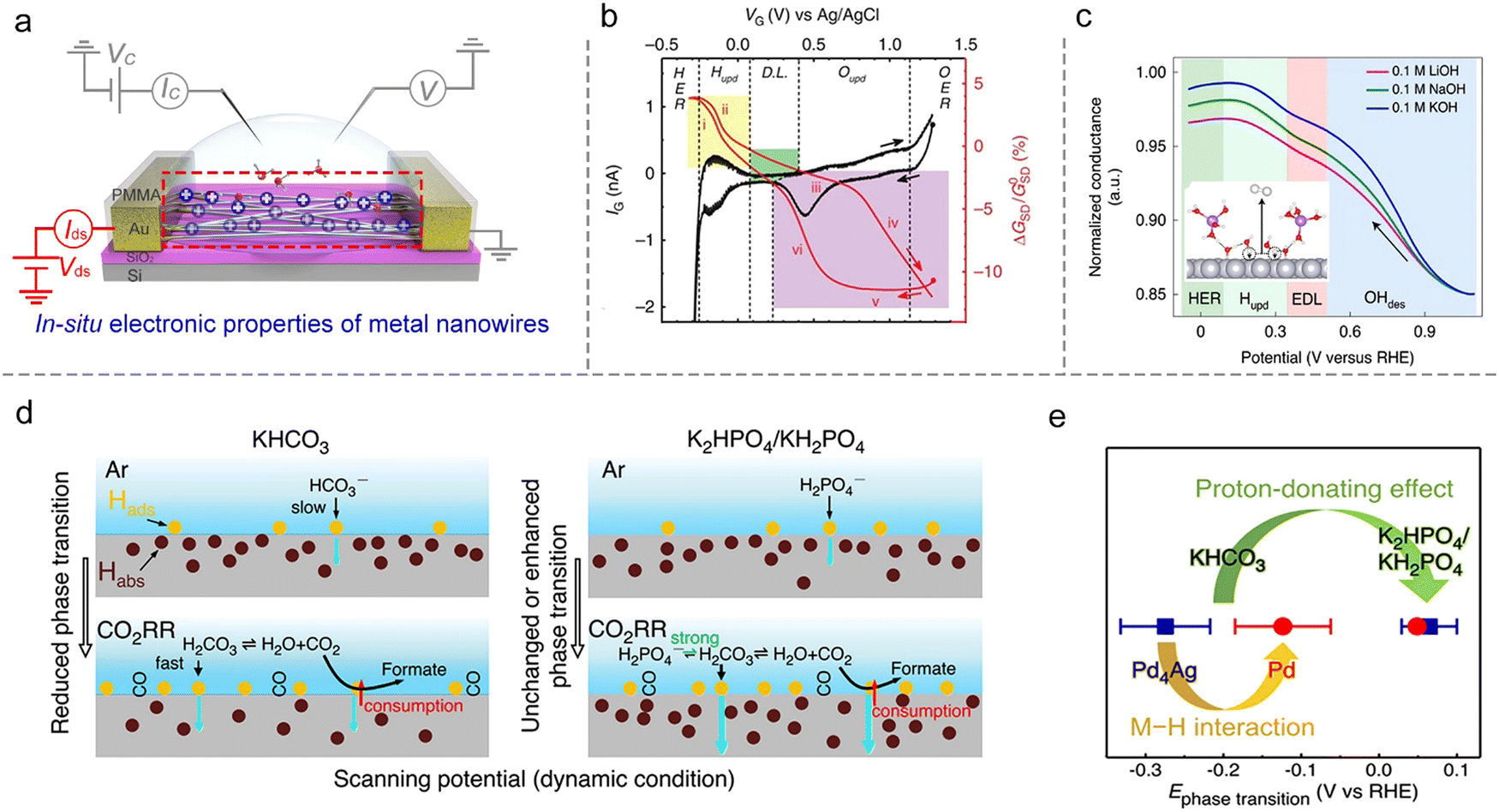 | ||
| Fig. 10 In situ conductance measurement on metal NWs. (a) Schematic illustration of the microcell-based in situ electronic/electrochemical measurement on metal NWs. (b) IG–VG curves (in black) and normalized GSD (conductance)–VG curves (in red) of a typical Pt NW microcell. (c) Normalized in situ conductance signal recorded at different potentials of the Pt NW device in 0.1 M MOH (M = Li, Na, and K) electrolyte. Inset: The Li+ enhances the coverage of OHad. (d) Schematic illustration of different Pd–H states at the interfaces in KHCO3 (left panel) and K2HPO4/KH2PO4 (right panel) during the CO2RR processes. The yellow and brown cycles represent the adsorbed H on the surface (Hads) and absorbed H in the bulk (Habs), respectively. (e) Summary of phase transition potentials of Pd (red) and Pd4Ag (blue) under CO2RR conditions in KHCO3 and K2HPO4/KH2PO4 obtained at 10 mV s−1. | ||
The first example is that Ding et al. developed a microcell to directly probe the electrochemical interfaces of Pt NWs.95 They showed that the electrical properties of ultrafine Pt NWs are susceptible and selective to the electrochemical surface states. The redox regions, e.g., HER, H adsorption/desorption region (Hupd), double layer (DL) region, surface oxide formation/reduction region (Oupd), and OER could be clearly distinguished from IG–VG and normalized GSD–VG curves, as shown in Fig. 10b. Using the microcell-based in situ measurement, they also examined a series of electrocatalytic reactions such as the H2O2 reduction and oxidation reactions, methanol oxidation reaction (MOR), and formic acid oxidation reaction (FOR), demonstrating the reliability and generality of this method.
Focusing on the influence of electrolytes on the HER, Duan et al. elaborated on the fundamental role of different cations (Li+, Na+, and K+) in HER kinetics using in situ charge transport measurement (Fig. 10c). By combining systematic experiments and theoretical studies, they concluded that the surface coverage of OHad was enhanced by the presence of small cations (Li+),25 as shown in Fig. 10c. Interestingly, such a method can be extendable to more complex electrochemical reactions such as the CO2 reduction reaction (CO2RR). For example, Ding et al. utilized microcells to monitor and quantify the H sorption process on different metallic NWs (Pd, Pt, Au, Pd4Ag) during the CO2RR process. The authors revealed a competitive relationship between electrochemical CO2RR and hydrogen sorption kinetics, related to the local electrolyte environment (proton donors with different pKa), as shown in Fig. 10d. Moreover, a more negative phase transition potential was also observed in Pd4Ag, giving direct evidence for the weakened M–H interaction in alloy catalysts to promote the CO2RR (Fig. 10e).96
5. Conclusion
The electrocatalytic strategies have attracted increasing research interest in developing clean and sustainable energy. However, the common particle-assembled measurement has faced several limitations, such as average results of thousands of samples, complex reaction interface, and unclear charge-flowing pathway in the electrodes. With the maturation of micro-nano processing technology, the on-chip microcell that provides an effective means to study the catalytic properties at a single NW/NS level, has shown growing potential in electrocatalysis. Table 1 highlights the current achievements based on on-chip electrocatalytic microcells. For example, making use of the reaction window, the on-chip microcell enables the identification of the active site or monitoring of its changes at a single nanomaterial level, such as (i) identification of the HER activity of GBs, edges, different phases and doping, and heterostructures, as well as (ii) monitoring of the phase transition, GB changes, and defect engineering. On the other hand, taking advantage of the circuits, many fantastic strategies can be developed to shed insight into the reaction behaviors, such as external electrical field modulation, contact engineering for charge injection, and in situ conductance measurements as well.| Strategies | Types | Materials | Performances | Electrolyte | Ref. |
|---|---|---|---|---|---|
| Identification | Phases | 1T′-MoS2 | HER: ηonset: 205 mV; Tafel slope: 51 mV dec−1 | 0.5 M H2SO4 | 57 |
| GBs | MoS2 nanograin film | HER: η10: 25 mV; Tafel slope: 54 mV dec−1 | 0.5 M H2SO4 | 48 | |
| 2H–1T-MoS2 GBs | HER: ηonset: 260 mV; Tafel slope: 85 mV dec−1 | 0.5 M H2SO4 | 58 | ||
| MoTe2 films | HER: ηonset: 211 mV; Tafel slope: 98 mV dec−1 | 0.5 M H2SO4 | 49 | ||
| Edges | 1T′-MoS2 | HER: ηonset: 77 mV; Tafel slope: 56 mV dec−1 | 0.5 M H2SO4 | 50 | |
| WTe2 flakes | HER: ηonset: 320 mV; Tafel slope: 110 mV dec−1 | 0.5 M H2SO4 | 59 | ||
| Doping | P-MoS2 | HER: η10: 297 mV; Tafel slope: 97 mV dec−1 | 0.5 M H2SO4 | 54 | |
| Mo-MoS2 | HER: ηonset: 107 mV; Tafel slope: 36.4 mV dec−1 | 0.5 M H2SO4 | 64 | ||
| HER: ηonset: 209 mV; Tafel slope: 35.1 mV dec−1 | 1.0 M KOH | ||||
| Monitoring | Amorphization | PtSex NSs | HER: smaller onset overpotential and Tafel slope with a treatment duration from 0 to 60s |
0.5 M H2SO4 | 10 |
| Defect engineering | MoTe2 NSs | HER: smaller onset overpotential and Tafel slope with an increase in the degree of oxidization | 0.5 M H2SO4 | 65 | |
| Thickness | Individual PtSe2 flakes | HER: smaller overpotential and Tafel slope with increasing layer numbers | 0.5 M H2SO4 | 51 | |
| Phase engineering | 1T′-MoS2 | HER: ηonset: 65 mV; Tafel slope: 100 mV dec−1 | 0.5 M H2SO4 | 66 | |
| External field regulation | Improve conductivity | MoS2 | HER: back-gate voltage 5 V, η100: 38 mV; Tafel slope: 110 mV dec−1 | 0.5 M H2SO4 | 75 |
| Back-gate voltage 0 V, η100: 240 mV; Tafel slope: 200 mV dec−1 | |||||
| Activate the intrinsic activity | MoS2 | HER: back-gate voltage −40 V, η50: 524 ± 8 mV; Tafel slope: 164 ± 1 mV dec−1 | 0.5 M H2SO4 | 79 | |
| Back-gate voltage 100V, η50: 334 ± 3 mV; Tafel slope: 100 ± 6 mV dec−1 | |||||
| WSe2 | HER: back-gate voltage 5 V, η10: 370 mV; Tafel slope: 138 mV dec−1 | 0.5 M H2SO4 | 80 | ||
| Back-gate voltage 20 V, η10: 280 mV; Tafel slope: 104 mV dec−1 | |||||
| CoPc/MoS2 | HER: back-gate voltage 2V, η10: 238 mV; Tafel slope: 115 mV dec−1 | 0.5 M H2SO4 | 81 | ||
| Pt SAs/MoS2 | HER: back-gate voltage from +60 V to −60 V, Δη50: 52 mV; Tafel slope: from 117 mV dec−1 to 65 mV dec−1 | 0.5 M H2SO4 | 82 | ||
| Co SAs/WSe2 | OER: back-gate voltage from +40 V to −40 V, Δη50: 104 mV; Tafel slope: from 281 mV dec−1 to 64 mV dec−1 | 0.1 M KOH | |||
| Induce the ion redistribution | VSe2 | HER: bate-gate voltage (0 V), η10: 126 mV; Tafel slope: 70 mV dec−1 | 0.5 M H2SO4 | 83 | |
| Bate-gate voltage (−1 V), η10: 70 mV; Tafel slope: 55 mV dec−1 | |||||
| Charge injection | Heterostructure | MoS2/graphene | HER: MoS2/graphene shows better performance than MoS2 with graphene contact | 0.5 M H2SO4 | 60 |
| Cr-doped WSe2/graphene | Overall water splitting: with a 310 mV reduction in cell voltage at 10 mA cm−2 compared to the Cr-doped WSe2 microcells with the gold contact | 1 M PBS | 90 | ||
| MoS2/WTe2 | HER: MoS2–WTe2 heterostructure shows the lowest overpotentials (−135 ± 5 mV) | 0.5 M H2SO4 | 91 | ||
| Phase transition | 2H MoS2 with 1T MoS2 contact | HER: basal plane of 2H MoS2 with low contact resistance is comparable to that of 1T phase and edge of 2H phase | 0.5 M H2SO4 | 20 | |
| In situ conductance measurement | Semiconductor catalyst | MoS2, WSe1.8Te0.2 and WSe2 | The type of semiconductor catalysts strongly correlate with their electrocatalysis | 0.5 M H2SO4 | 94 |
| MoS2 | HER: electrolyte gating lowering the contact resistance | 0.5 M H2SO4 | 95 | ||
| Metallic catalyst | Pt NWs | Providing a new strategy to in situ monitor the electrochemical surface conditions of metal nanocatalysts | 0.5 M H2SO4 | 96 | |
| Pt NWs | Smaller cations favor a high OHad coverage on the Pt surface in the HER potential window | 0.1 M KOH LiOH or NaOH | 25 | ||
| Pd NWs and Pd4Ag NWs | The proton-donating capacity of near neutral electrolytes serve as a key impacting factor to H sorption kinetics and CO2RR | KHCO3 or K2HPO4/KH2PO4 | 97 |
Although significant progress has been made on on-chip electrocatalytic microcells over the last decade, its research is still in its infancy. There would be a long way to explore its true potential. Hence, we propose our prospects in this emerging field, as illustrated in Fig. 11.
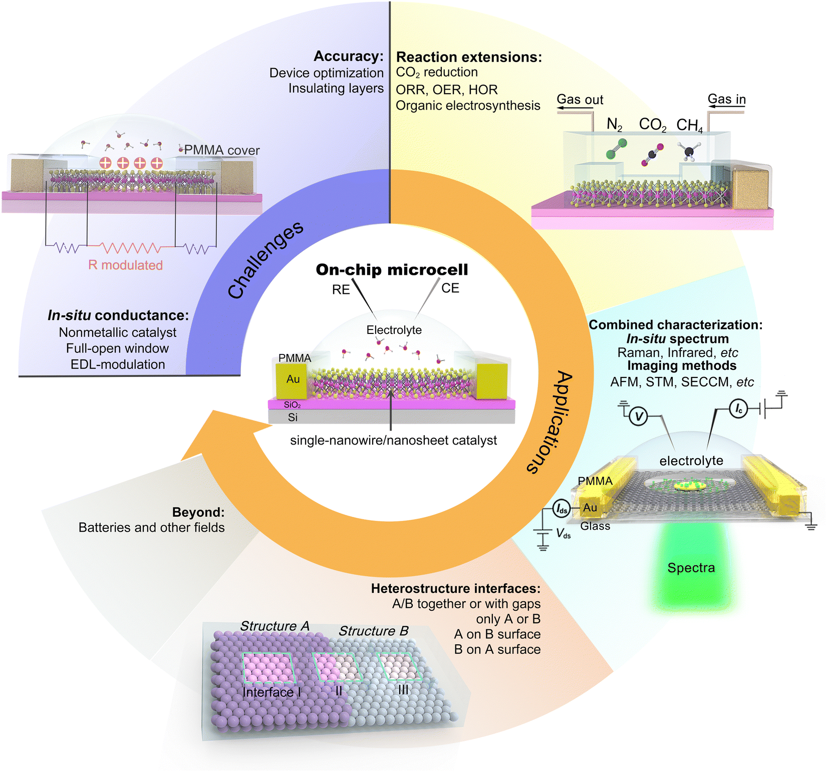 | ||
| Fig. 11 Prospects for on-chip microcells. The challenges in this emergent field, such as measurement accuracy and the conductance issue, are discussed. The applications of the on-chip microcells, e.g., the generality (reaction extension), guidance (model catalysis), multi-functions (combined strategy), and others, are also expected. | ||
5.1 Challenges
5.2 Applications
The on-chip microcell can be expandable to other fields, such as photovoltaics, photoelectrochemical, thermoelectric, and electrodialysis. For example, in photovoltaics, as early as 2007, Lieber et al. reported an on-chip single p–i–n silicon nanowire solar cell.106 In photoelectrochemistry, Geim et al. reported a strong dependence of the photoelectrochemical properties on the number of MoS2 layers with the help of an on-chip platform.107 In thermoelectrics, Zeng et al. investigated the thermoelectric transport of 2D indium selenide (InSe) with different thicknesses under the gate voltages.108 In electrodialysis, Geim et al. investigated a series of monolayer crystals to explore the proton transport properties of the atomic-thick layer, promoting the development of electrodialysis and the utilization of blue energy.109 Based on those efforts, more tantalizing applications are encouraged to be underway and come to fruition shortly.
Conflicts of interest
The authors declare no conflict of interest.Acknowledgements
Y. H. acknowledges the National Key R&D Program of China (2021YFA1500900), the Fundamental Research Funds for Central Universities (531119200209), and the National Natural Science Foundation of China (52203354 and 22272048).References
- W. Ahmad, P. Koley, S. Dwivedi, R. Lakshman, Y. K. Shin, A. C. T. van Duin, A. Shrotri and A. Tanksale, Nat. Commun., 2023, 14, 304 CrossRef PubMed.
- X. Zhu, H. Zong, C. J. V. Pérez, H. Miao, W. Sun, Z. Yuan, S. Wang, G. Zeng, H. Xu, Z. Jiang and G. A. Ozin, Angew. Chem., Int. Ed., 2023, 62, e2022186 Search PubMed.
- H. Nishiyama, T. Yamada, M. Nakabayashi, Y. Maehara, M. Yamaguchi, Y. Kuromiya, Y. Nagatsuma, H. Tokudome, S. Akiyama, T. Watanabe, R. Narushima, S. Okunaka, N. Shibata, T. Takata, T. Hisatomi and K. Domen, Nature, 2021, 598, 304–307 CrossRef CAS PubMed.
- P. Zhou, I. A. Navid, Y. Ma, Y. Xiao, P. Wang, Z. Ye, B. Zhou, K. Sun and Z. Mi, Nature, 2023, 613, 66–70 CrossRef CAS.
- T. S. Teitsworth, D. J. Hill, S. R. Litvin, E. T. Ritchie, J.-S. Park, J. P. Custer, A. D. Taggart, S. R. Bottum, S. E. Morley, S. Kim, J. R. McBride, J. M. Atkin and J. F. Cahoon, Nature, 2023, 614, 270–274 CrossRef CAS PubMed.
- Y. Jiao, Y. Zheng, M. Jaroniec and S. Z. Qiao, Chem. Soc. Rev., 2015, 44, 2060–2086 RSC.
- M. Liu, Y. Pang, B. Zhang, P. De Luna, O. Voznyy, J. Xu, X. Zheng, C. T. Dinh, F. Fan, C. Cao, F. P. G. de Arquer, T. S. Safaei, A. Mepham, A. Klinkova, E. Kumacheva, T. Filleter, D. Sinton, S. O. Kelley and E. H. Sargent, Nature, 2016, 537, 382–386 CrossRef CAS PubMed.
- C. Chen, X. Zhu, X. Wen, Y. Zhou, L. Zhou, H. Li, L. Tao, Q. Li, S. Du, T. Liu, D. Yan, C. Xie, Y. Zou, Y. Wang, R. Chen, J. Huo, Y. Li, J. Cheng, H. Su, X. Zhao, W. Cheng, Q. Liu, H. Lin, J. Luo, J. Chen, M. Dong, K. Cheng, C. Li and S. Wang, Nat. Chem., 2020, 12, 717–724 CrossRef CAS PubMed.
- Q. Wang, T. Li, C. Yang, M. Chen, A. Guan, L. Yang, S. Li, X. Lv, Y. Wang and G. Zheng, Angew. Chem., Int. Ed., 2021, 60, 17398–17403 CrossRef CAS PubMed.
- Y. He, L. Liu, C. Zhu, S. Guo, P. Golani, B. Koo, P. Tang, Z. Zhao, M. Xu, C. Zhu, P. Yu, X. Zhou, C. Gao, X. Wang, Z. Shi, L. Zheng, J. Yang, B. Shin, J. Arbiol, H. Duan, Y. Du, M. Heggen, R. E. Dunin-Borkowski, W. Guo, Q. J. Wang, Z. Zhang and Z. Liu, Nat. Catal., 2022, 5, 212–221 CrossRef CAS.
- P. Garrido-Barros, J. Derosa, M. J. Chalkley and J. C. Peters, Nature, 2022, 609, 71–76 CrossRef CAS PubMed.
- B. Zhu, B. Dong, F. Wang, Q. Yang, Y. He, C. Zhang, P. Jin and L. Feng, Nat. Commun., 2023, 14, 1686 CrossRef CAS PubMed.
- W. Shao, M. Xiao, C. Yang, M. Cheng, S. Cao, C. He, M. Zhou, T. Ma, C. Cheng and S. Li, Small, 2021, 18, 2105763 CrossRef PubMed.
- Y. j Wu, J. Yang, T. x Tu, W. q Li, P. f Zhang, Y. Zhou, J. f Li, J. t Li and S. G. Sun, Angew. Chem., Int. Ed., 2021, 60, 26829–26836 CrossRef CAS PubMed.
- S. Song, J. Zhou, X. Su, Y. Wang, J. Li, L. Zhang, G. Xiao, C. Guan, R. Liu, S. Chen, H.-J. Lin, S. Zhang and J.-Q. Wang, Energy Environ. Sci., 2018, 11, 2945–2953 RSC.
- A. L. Strickler, M. a Escudero-Escribano and T. F. Jaramillo, Nano Lett., 2017, 17, 6040–6046 CrossRef CAS PubMed.
- H. Jin, S. Choi, G. J. Bang, T. Kwon, H. S. Kim, S. J. Lee, Y. Hong, D. W. Lee, H. S. Park, H. Baik, Y. Jung, S. J. Yoo and K. Lee, Energy Environ. Sci., 2022, 15, 1119–1130 RSC.
- L. Mai, Y. Dong, L. Xu and C. Han, Nano Lett., 2010, 10, 4273–4278 CrossRef CAS PubMed.
- M. Ding, Q. He, G. Wang, H.-C. Cheng, Y. Huang and X. Duan, Nat. Commun., 2015, 6, 7867 CrossRef CAS PubMed.
- D. Voiry, R. Fullon, J. Yang, E. S. C. de Carvalho Castro, R. Kappera, I. Bozkurt, D. Kaplan, M. J. Lagos, P. E. Batson, G. Gupta, A. D. Mohite, L. Dong, D. Er, V. B. Shenoy, T. Asefa and M. Chhowalla, Nat. Mater., 2016, 15, 1003–1009 CrossRef CAS PubMed.
- J. Qi, W. Wang, Y. Li, Y. Sun, Z. Wu, K. Bao, L. Wang, R. Ye, M. Ding and Q. He, Small, 2022, 18, 2204010 CrossRef CAS PubMed.
- C.-H. Kim and C. D. Frisbie, J. Am. Chem. Soc., 2016, 138, 7220–7223 CrossRef CAS PubMed.
- Y. Wang, C.-H. Kim, Y. Yoo, J. E. Johns and C. D. Frisbie, Nano Lett., 2017, 17, 7586–7592 CrossRef CAS PubMed.
- Y. He, Q. He, L. Wang, C. Zhu, P. Golani, A. D. Handoko, X. Yu, C. Gao, M. Ding, X. Wang, F. Liu, Q. Zeng, P. Yu, S. Guo, B. I. Yakobson, L. Wang, Z. W. Seh, Z. Zhang, M. Wu, Q. J. Wang, H. Zhang and Z. Liu, Nat. Mater., 2019, 18, 1098–1104 CrossRef CAS PubMed.
- A. H. Shah, Z. Zhang, Z. Huang, S. Wang, G. Zhong, C. Wan, A. N. Alexandrova, Y. Huang and X. Duan, Nat. Catal., 2022, 5, 923–933 CrossRef CAS.
- S. Najmaei, A. L. Glasmann, M. A. Schroeder, W. L. Sarney, M. L. Chin and D. M. Potrepka, Mater. Today, 2022, 59, 80–106 CrossRef CAS.
- J. A. del Alamo, Nature, 2011, 479, 317–323 CrossRef CAS PubMed.
- I. Ferain, C. A. Colinge and J.-P. Colinge, Nature, 2011, 479, 310–316 CrossRef CAS PubMed.
- Z. Cheng, C.-S. Pang, P. Wang, S. T. Le, Y. Wu, D. Shahrjerdi, I. Radu, M. C. Lemme, L.-M. Peng, X. Duan, Z. Chen, J. Appenzeller, S. J. Koester, E. Pop, A. D. Franklin and C. A. Richter, Nat. Electron., 2022, 5, 416–423 CrossRef.
- H. Du, X. Lin, Z. Xu and D. Chu, J. Mater. Sci., 2015, 50, 5641–5673 CrossRef CAS.
- B. Radisavljevic, A. Radenovic, J. Brivio, V. Giacometti and A. Kis, Nat. Nanotechnol., 2011, 6, 147–150 CrossRef CAS PubMed.
- Y. Wu, S. Ringe, C.-L. Wu, W. Chen, A. Yang, H. Chen, M. Tang, G. Zhou, H. Y. Hwang, K. Chan and Y. Cui, Nano Lett., 2019, 19, 7293–7300 CrossRef CAS PubMed.
- Y.-G. Ha, K. Everaerts, M. C. Hersam and T. J. Marks, Acc. Chem. Res., 2014, 47, 1019–1028 CrossRef CAS PubMed.
- F. Torricelli, D. Z. Adrahtas, Z. Bao, M. Berggren, F. Biscarini, A. Bonfiglio, C. A. Bortolotti, C. D. Frisbie, E. Macchia, G. G. Malliaras, I. McCulloch, M. Moser, T. Q. Nguyen, R. M. Owens, A. Salleo, A. Spanu and L. Torsi, Nat. Rev. Methods Primers, 2021, 1, 66 CrossRef CAS PubMed.
- P. Liu, B. Lei, X. Chen, L. Wang and X. Wang, Nat. Rev. Phys., 2022, 4, 336–352 CrossRef CAS.
- S. Z. Bisri, S. Shimizu, M. Nakano and Y. Iwasa, Adv. Mater., 2017, 29, 1607054 CrossRef.
- Y. J. Zhang, J. T. Ye, Y. Yomogida, T. Takenobu and Y. Iwasa, Nano Lett., 2013, 13, 3023–3028 CrossRef CAS PubMed.
- C. Leighton, Nat. Mater., 2019, 18, 13–18 CrossRef CAS PubMed.
- S. H. Kim, K. Hong, W. Xie, K. H. Lee, S. Zhang, T. P. Lodge and C. D. Frisbie, Adv. Mater., 2013, 25, 1822–1846 CrossRef CAS PubMed.
- M. Nakano, K. Shibuya, D. Okuyama, T. Hatano, S. Ono, M. Kawasaki, Y. Iwasa and Y. Tokura, Nature, 2012, 487, 459–462 CrossRef CAS PubMed.
- X. Tong, Y. Zhao, Z. Zhuo, Z. Yang, S. Wang, Y. Liu, N. Lu, H. Li and T. Zhai, Angew. Chem., Int. Ed., 2022, 61, e202112953 CrossRef CAS PubMed.
- W. Wang, Y. Song, C. Ke, Y. Li, Y. Liu, C. Ma, Z. Wu, J. Qi, K. Bao, L. Wang, J. Wu, S. Jiang, J. Zhao, C.-S. Lee, Y. Chen, G. Luo, Q. He and R. Ye, ACS Nano, 2023, 17, 1287–1297 CrossRef CAS PubMed.
- Z. Mu, M. Yang, W. He, Y. Pan, P. Zhang, X. Li, X. Wu and M. Ding, J. Phys. Chem. Lett., 2020, 11, 5798–5806 CrossRef CAS PubMed.
- B. Tian, H. Shin, S. Liu, M. Fei, Z. Mu, C. Liu, Y. Pan, Y. Sun, W. A. Goddard, 3rd and M. Ding, Angew. Chem., Int. Ed., 2021, 60, 16448–16456 CrossRef CAS PubMed.
- H. Xia, Z. Shi, C. Gong and Y. He, J. Mater. Chem. A, 2022, 10, 19067–19089 RSC.
- D. Voiry, M. Salehi, R. Silva, T. Fujita, M. Chen, T. Asefa, V. B. Shenoy, G. Eda and M. Chhowalla, Nano Lett., 2013, 13, 6222–6227 CrossRef CAS PubMed.
- Y. Chen, Z. Lai, X. Zhang, Z. Fan, Q. He, C. Tan and H. Zhang, Nat. Rev. Chem., 2020, 4, 243–256 CrossRef CAS PubMed.
- Y. He, P. Tang, Z. Hu, Q. He, C. Zhu, L. Wang, Q. Zeng, P. Golani, G. Gao, W. Fu, Z. Huang, C. Gao, J. Xia, X. Wang, X. Wang, C. Zhu, Q. M. Ramasse, A. Zhang, B. An, Y. Zhang, S. Marti-Sanchez, J. R. Morante, L. Wang, B. K. Tay, B. I. Yakobson, A. Trampert, H. Zhang, M. Wu, Q. J. Wang, J. Arbiol and Z. Liu, Nat. Commun., 2020, 11, 57 CrossRef CAS.
- Y. Lee, N. Ling, D. Kim, M. Zhao, Y. A. Eshete, E. Kim, S. Cho and H. Yang, Adv. Funct. Mater., 2021, 32, 2105675 CrossRef.
- J. Zhang, J. Wu, H. Guo, W. Chen, J. Yuan, U. Martinez, G. Gupta, A. Mohite, P. M. Ajayan and J. Lou, Adv. Mater., 2017, 29, 1701955 CrossRef PubMed.
- D. Hu, T. Zhao, X. Ping, H. Zheng, L. Xing, X. Liu, J. Zheng, L. Sun, L. Gu, C. Tao, D. Wang and L. Jiao, Angew. Chem., Int. Ed., 2019, 58, 6977–6981 CrossRef CAS PubMed.
- Y. Zang, S. Niu, Y. Wu, X. Zheng, J. Cai, J. Ye, Y. Xie, Y. Liu, J. Zhou, J. Zhu, X. Liu, G. Wang and Y. Qian, Nat. Commun., 2019, 10, 1217 CrossRef.
- Z. Zheng, L. Yu, M. Gao, X. Chen, W. Zhou, C. Ma, L. Wu, J. Zhu, X. Meng, J. Hu, Y. Tu, S. Wu, J. Mao, Z. Tian and D. Deng, Nat. Commun., 2020, 11, 3315 CrossRef CAS.
- W. Wang, Y. Song, C. Ke, Y. Li, Y. Liu, C. Ma, Z. Wu, J. Qi, K. Bao, L. Wang, J. Wu, S. Jiang, J. Zhao, C. S. Lee, Y. Chen, G. Luo, Q. He and R. Ye, ACS Nano, 2023, 17, 1287–1297 CrossRef CAS.
- M. A. Lukowski, A. S. Daniel, F. Meng, A. Forticaux, L. Li and S. Jin, J. Am. Chem. Soc., 2013, 135, 10274–10277 CrossRef CAS PubMed.
- H. Wang, Z. Lu, S. Xu, D. Kong, J. J. Cha, G. Zheng, P.-C. Hsu, K. Yan, D. Bradshaw, F. B. Prinz and Y. Cui, Proc. Natl. Acad. Sci. U. S. A., 2013, 110, 19701–19706 CrossRef CAS PubMed.
- L. Liu, J. Wu, L. Wu, M. Ye, X. Liu, Q. Wang, S. Hou, P. Lu, L. Sun, J. Zheng, L. Xing, L. Gu, X. Jiang, L. Xie and L. Jiao, Nat. Mater., 2018, 17, 1108–1114 CrossRef CAS PubMed.
- J. Zhu, Z. C. Wang, H. Dai, Q. Wang, R. Yang, H. Yu, M. Liao, J. Zhang, W. Chen, Z. Wei, N. Li, L. Du, D. Shi, W. Wang, L. Zhang, Y. Jiang and G. Zhang, Nat. Commun., 2019, 10, 1348 CrossRef PubMed.
- Y. Zhou, J. L. Silva, J. M. Woods, J. V. Pondick, Q. Feng, Z. Liang, W. Liu, L. Lin, B. Deng, B. Brena, F. Xia, H. Peng, Z. Liu, H. Wang, C. M. Araujo and J. J. Cha, Adv. Mater., 2018, 30, e1706076 CrossRef PubMed.
- D. Gao, B. Xia, C. Zhu, Y. Du, P. Xi, D. Xue, J. Ding and J. Wang, J. Mater. Chem. A, 2018, 6, 510–515 RSC.
- S. S. Chee, H. Jang, K. Lee and M. H. Ham, ACS Appl. Mater. Interfaces, 2020, 12, 31804–31809 CrossRef CAS PubMed.
- W. Xiao, P. Liu, J. Zhang, W. Song, Y. P. Feng, D. Gao and J. Ding, Adv. Energy Mater., 2017, 7, 1602086 CrossRef.
- P. Liu, J. Zhu, J. Zhang, P. Xi, K. Tao, D. Gao and D. Xue, ACS Energy Lett., 2017, 2, 745–752 CrossRef CAS.
- Y. Luo, S. Zhang, H. Pan, S. Xiao, Z. Guo, L. Tang, U. Khan, B. F. Ding, M. Li, Z. Cai, Y. Zhao, W. Lv, Q. Feng, X. Zou, J. Lin, H. M. Cheng and B. Liu, ACS Nano, 2020, 14, 767–776 CrossRef CAS PubMed.
- H. You, Z. Zhuo, X. Lu, Y. Liu, Y. Guo, W. Wang, H. Yang, X. Wu, H. Li and T. Zhai, CCS Chem., 2019, 1, 396–406 CrossRef CAS.
- Y. Yu, G. H. Nam, Q. He, X. J. Wu, K. Zhang, Z. Yang, J. Chen, Q. Ma, M. Zhao, Z. Liu, F. R. Ran, X. Wang, H. Li, X. Huang, B. Li, Q. Xiong, Q. Zhang, Z. Liu, L. Gu, Y. Du, W. Huang and H. Zhang, Nat. Chem., 2018, 10, 638–643 CrossRef CAS PubMed.
- M. Yan, X. Zhou, X. Pan, J. Wang, L. Xia, K. Yu, X. Liao, X. Xu, L. He and L. Mai, Nano Res., 2018, 11, 3205–3212 CrossRef CAS.
- C. H. Kim, Y. Wang and C. D. Frisbie, Anal. Chem., 2019, 91, 1627–1635 CrossRef CAS PubMed.
- W. Zhang, X. Liao, X. Pan, M. Yan, Y. Li, X. Tian, Y. Zhao, L. Xu and L. Mai, Small, 2019, 15, e1900964 CrossRef PubMed.
- H. Xiang, Y. Zheng, Y. Chen, Y. Xu, T. S. Hu, Y. Feng, Y. Zhou, S. Liu and X. Chen, Chin. Chem. Lett., 2022, 33, 3221–3226 CrossRef CAS.
- M. Ding, G. Zhong, Z. Zhao, Z. Huang, M. Li, H. Y. Shiu, Y. Liu, I. Shakir, Y. Huang and X. Duan, ACS Cent. Sci., 2018, 4, 590–599 CrossRef CAS PubMed.
- H. Yang, Q. He, Y. Liu, H. Li, H. Zhang and T. Zhai, Chem. Soc. Rev., 2020, 49, 2916–2936 RSC.
- X. Zhu, C. Wang and L. Fu, Cell Rep. Phys. Sci., 2020, 1, 100190 CrossRef.
- J. Wang, M. Yan, K. Zhao, X. Liao, P. Wang, X. Pan, W. Yang and L. Mai, Adv. Mater., 2017, 29, 1604464 CrossRef PubMed.
- F. L. Ling, T. W. Zhou, X. Q. Liu, W. Kang, W. Zeng, Y. X. Zhang, L. Fang, Y. Lu and M. Zhou, Nanotechnology, 2018, 29, 03LT01 CrossRef CAS PubMed.
- C. V. Nguyen, Superlattices Microstruct., 2018, 116, 79–87 CrossRef CAS.
- T. V. Vu, N. V. Hieu, L. T. P. Thao, N. N. Hieu, H. V. Phuc, H. D. Bui, M. Idrees, B. Amin, L. M. Duc and C. V. Nguyen, Phys. Chem. Chem. Phys., 2019, 21, 22140–22148 RSC.
- Y. Wang, S. Udyavara, M. Neurock and C. D. Frisbie, Nano Lett., 2019, 19, 6118–6123 CrossRef CAS PubMed.
- Z. Wang, H. H. Wu, Q. Li, F. Besenbacher, Y. Li, X. C. Zeng and M. Dong, Adv. Sci., 2020, 7, 1901382 CrossRef CAS PubMed.
- J. Huang, Z. Zhuang, Y. Zhao, J. Chen, Z. Zhuo, Y. Liu, N. Lu, H. Li and T. Zhai, Angew. Chem., Int. Ed., 2022, 61, e202203522 CrossRef CAS PubMed.
- Y. Pan, X. Wang, W. Zhang, L. Tang, Z. Mu, C. Liu, B. Tian, M. Fei, Y. Sun, H. Su, L. Gao, P. Wang, X. Duan, J. Ma and M. Ding, Nat. Commun., 2022, 13, 3063 CrossRef CAS PubMed.
- M. Yan, X. Pan, P. Wang, F. Chen, L. He, G. Jiang, J. Wang, J. Z. Liu, X. Xu, X. Liao, J. Yang and L. Mai, Nano Lett., 2017, 17, 4109–4115 CrossRef CAS PubMed.
- Y. Liu, J. Guo, E. Zhu, L. Liao, S. J. Lee, M. Ding, I. Shakir, V. Gambin, Y. Huang and X. Duan, Nature, 2018, 557, 696–700 CrossRef CAS PubMed.
- A. Allain, J. Kang, K. Banerjee and A. Kis, Nat. Mater., 2015, 14, 1195–1205 CrossRef CAS PubMed.
- H. Murata, Y. Nakajima, N. Saitoh, N. Yoshizawa, T. Suemasu and K. Toko, Sci. Rep., 2019, 9, 4068 CrossRef.
- C. H. Lui, L. Liu, K. F. Mak, G. W. Flynn and T. F. Heinz, Nature, 2009, 462, 339–341 CrossRef CAS.
- W. J. Yu, Z. Li, H. Zhou, Y. Chen, Y. Wang, Y. Huang and X. Duan, Nat. Mater., 2013, 12, 246–252 CrossRef CAS PubMed.
- A. Allain, J. Kang, K. Banerjee and A. Kis, Nat. Mater., 2015, 14, 1195 CrossRef CAS PubMed.
- C. H. Chiang, Y. C. Yang, J. W. Lin, Y. C. Lin, P. T. Chen, C. L. Dong, H. M. Lin, K. M. Chan, Y. T. Kao, K. Suenaga, P. W. Chiu and C. W. Chen, ACS Nano, 2022, 16, 18274–18283 CrossRef CAS PubMed.
- Y. Zhou, J. V. Pondick, J. L. Silva, J. M. Woods, D. J. Hynek, G. Matthews, X. Shen, Q. Feng, W. Liu, Z. Lu, Z. Liang, B. Brena, Z. Cai, M. Wu, L. Jiao, S. Hu, H. Wang, C. M. Araujo and J. J. Cha, Small, 2019, 15, e1900078 CrossRef PubMed.
- Y. Chen, K. Yang, B. Jiang, J. Li, M. Zeng and L. Fu, J. Mater. Chem. A, 2017, 5, 8187–8208 RSC.
- J. Wu, Chem. Rev., 2022, 122, 10821–10859 CrossRef CAS PubMed.
- Y. He, Q. He, L. Wang, C. Zhu, P. Golani, A. D. Handoko, X. Yu, C. Gao, M. Ding, X. Wang, F. Liu, Q. Zeng, P. Yu, S. Guo, B. I. Yakobson, L. Wang, Z. W. she, Z. Zhang, M. Wu, Q. J. Wang, H. Zhang and Z. Liu, Nat. Mater., 2019, 18, 1098–1104 CrossRef CAS PubMed.
- X. Liu, B. Li, X. Li, A. R. Harutyunyan, J. Hone and D. V. Esposito, Nano Lett., 2019, 19, 8118–8124 CrossRef CAS PubMed.
- M. Ding, Q. He, G. Wang, H. C. Cheng, Y. Huang and X. Duan, Nat. Commun., 2015, 6, 7867 CrossRef CAS PubMed.
- Z. Mu, N. Han, D. Xu, B. Tian, F. Wang, Y. Wang, Y. Sun, C. Liu, P. Zhang, X. Wu, Y. Li and M. Ding, Nat. Commun., 2022, 13, 6911 CrossRef CAS PubMed.
- X. Zhang, M. Zhang, Y. Deng, M. Xu, L. Artiglia, W. Wen, R. Gao, B. Chen, S. Yao, X. Zhang, M. Peng, J. Yan, A. Li, Z. Jiang, X. Gao, S. Cao, C. Yang, A. J. Kropf, J. Shi, J. Xie, M. Bi, J. A. van Bokhoven, Y.-W. Li, X. Wen, M. Flytzani-Stephanopoulos, C. Shi, W. Zhou and D. Ma, Nature, 2021, 589, 396–401 CrossRef CAS.
- N. Clark, D. J. Kelly, M. Zhou, Y.-C. Zou, C. W. Myung, D. G. Hopkinson, C. Schran, A. Michaelides, R. Gorbachev and S. J. Haigh, Nature, 2022, 609, 942–947 CrossRef CAS.
- Y. Zhao, X.-G. Zhang, N. Bodappa, W.-M. Yang, Q. Liang, P. M. Radjenovica, Y.-H. Wang, Y.-J. Zhang, J.-C. Dong, Z.-Q. Tian and J.-F. Li, Energy Environ. Sci., 2022, 15, 3968–3977 RSC.
- X. Zhou, J. Shan, L. Chen, B. Y. Xia, T. Ling, J. Duan, Y. Jiao, Y. Zheng and S.-Z. Qiao, J. Am. Chem. Soc., 2022, 144, 2079–2084 CrossRef CAS PubMed.
- K. Sun, X. Wu, Z. Zhuang, L. Liu, J. Fang, L. Zeng, J. Ma, S. Liu, J. Li, R. Dai, X. Tan, K. Yu, D. Liu, W.-C. Cheong, A. Huang, Y. Liu, Y. Pan, H. Xiao and C. Chen, Nat. Commun., 2022, 13, 6260 CrossRef CAS PubMed.
- R. Ge, Y. Wang, Z. Li, M. Xu, S. M. Xu, H. Zhou, K. Ji, F. Chen, J. Zhou and H. Duan, Angew. Chem., Int. Ed., 2022, 61, e202200211 CrossRef CAS PubMed.
- R. Hao, Y. Fan, M. D. Howard, J. C. Vaughan and B. Zhang, Proc. Natl. Acad. Sci. U. S. A., 2018, 115, 5878–5883 CrossRef CAS PubMed.
- H. Han, Q. Jacquet, Z. Jiang, F. N. Sayed, J.-C. Jeon, A. Sharma, A. M. Schankler, A. Kakekhani, H. L. Meyerheim, J. Park, S. Y. Nam, K. J. Griffith, L. Simonelli, A. M. Rappe, C. P. Grey and S. S. P. Parkin, Nat. Mater., 2023, 22, 1128–1135 CrossRef CAS PubMed.
- A. Yang, G. Zhou, X. Kong, R. A. Vilá, A. Pei, Y. Wu, X. Yu, X. Zheng, C.-L. Wu, B. Liu, H. Chen, Y. Xu, D. Chen, Y. Li, S. Fakra, H. Y. Hwang, J. Qin, S. Chu and Y. Cui, Nat. Nanotechnol., 2020, 15, 231–237 CrossRef CAS PubMed.
- B. Tian, X. Zheng, T. J. Kempa, Y. Fang, N. Yu, G. Yu, J. Huang and C. M. Lieber, Nature, 2007, 449, 885–889 CrossRef CAS PubMed.
- M. Velický, M. A. Bissett, C. R. Woods, P. S. Toth, T. Georgiou, I. A. Kinloch, K. S. Novoselov and R. A. W. Dryfe, Nano Lett., 2016, 16, 2023–2032 CrossRef PubMed.
- J. Zeng, X. He, S.-J. Liang, E. Liu, Y. Sun, C. Pan, Y. Wang, T. Cao, X. Liu, C. Wang, L. Zhang, S. Yan, G. Su, Z. Wang, K. Watanabe, T. Taniguchi, D. J. Singh, L. Zhang and F. Miao, Nano Lett., 2018, 18, 7538–7545 CrossRef CAS PubMed.
- S. Hu, M. Lozada-Hidalgo, F. C. Wang, A. Mishchenko, F. Schedin, R. R. Nair, E. W. Hill, D. W. Boukhvalov, M. I. Katsnelson, R. A. W. Dryfe, I. V. Grigorieva, H. A. Wu and A. K. Geim, Nature, 2014, 516, 227–230 CrossRef CAS PubMed.
Footnote |
| † These authors contributed equally to this work. |
| This journal is © The Royal Society of Chemistry 2023 |