
Efficient monolithic perovskite–Si tandem solar cells enabled by an ultra-thin indium tin oxide interlayer†
Jianghui
Zheng‡
 *abcd,
Weiyuan
Duan‡
e,
Yuzhen
Guo
a,
Zijun C.
Zhao
af,
Haimang
Yi
c,
Fa-Jun
Ma
c,
Laura
Granados Caro
ab,
Chuqi
Yi
c,
Jueming
Bing
ab,
Shi
Tang
ab,
Jiangtao
Qu
g,
Kean Chern
Fong
h,
Xin
Cui
c,
Yan
Zhu
c,
Limei
Yang
gi,
Andreas
Lambertz
e,
Md
Arafat Mahmud
ab,
Hongjun
Chen
ab,
Chwenhaw
Liao
ab,
Guoliang
Wang
ab,
Marko
Jankovec
j,
Cheng
Xu
c,
Ashraf
Uddin
c,
Julie M.
Cairney
g,
Stephen
Bremner
c,
Shujuan
Huang
cd,
Kaining
Ding
*e,
David R.
McKenzie
a and
Anita W. Y.
Ho-Baillie
*abc
*abcd,
Weiyuan
Duan‡
e,
Yuzhen
Guo
a,
Zijun C.
Zhao
af,
Haimang
Yi
c,
Fa-Jun
Ma
c,
Laura
Granados Caro
ab,
Chuqi
Yi
c,
Jueming
Bing
ab,
Shi
Tang
ab,
Jiangtao
Qu
g,
Kean Chern
Fong
h,
Xin
Cui
c,
Yan
Zhu
c,
Limei
Yang
gi,
Andreas
Lambertz
e,
Md
Arafat Mahmud
ab,
Hongjun
Chen
ab,
Chwenhaw
Liao
ab,
Guoliang
Wang
ab,
Marko
Jankovec
j,
Cheng
Xu
c,
Ashraf
Uddin
c,
Julie M.
Cairney
g,
Stephen
Bremner
c,
Shujuan
Huang
cd,
Kaining
Ding
*e,
David R.
McKenzie
a and
Anita W. Y.
Ho-Baillie
*abc
aSchool of Physics, The University of Sydney, Sydney, NSW 2006, Australia. E-mail: jianghui.zheng@sydney.edu.au; anita.ho-baillie@sydney.edu.au
bThe University of Sydney Nano Institute (Sydney Nano), The University of Sydney, Sydney, NSW 2006, Australia
cAustralian Centre for Advanced Photovoltaics (ACAP), School of Photovoltaic and Renewable Energy Engineering, University of New South Wales, Sydney 2052, Australia
dSustainable Energy Research Centre, School of Engineering, Macquarie University, Sydney, NSW 2109, Australia
eIEK-5 Photovoltaics, Forschungszentrum Jülich GmbH, 52428 Jülich, Germany. E-mail: k.ding@fz-juelich.de
fARC Centre of Excellence for Engineered Quantum Systems and ARC Centre of Excellence for Dark Matter Particle Physics, Department of Physics, University of Western Australia, Western Australia 6009, Australia
gAustralian Centre for Microscopy and Microanalysis (ACMM), The University of Sydney, Sydney, NSW 2006, Australia
hResearch School of Engineering, The Australian National University, Canberra, ACT 2601, Australia
iSchool of Civil & Environmental Engineering, University of Technology Sydney, 81 Broadway, Ultimo, NSW 2007, Australia
jFaculty of Electrical Engineering, University of Ljubljana, Trzaska 25, Ljubljana 1000, Slovenia
First published on 26th January 2023
Abstract
Tandem solar cells are promising for overcoming the theoretical single junction solar cell efficiency limit. Here we report an elegant approach to monolithically integrate perovskites and Si-heterojunction tandem solar cells using an ultra-thin indium tin oxide (ITO) interlayer. It is found that a 1.7 nm ITO interlayer is sufficient to provide the interfacing between the silicon and perovskite subcells with minimum parasitic resistance and efficient trap states for carrier recombination. Thinner ITO interlayers result in discontinuous films while thicker ITO interlayers with improved lateral conductivity are less effective in localising shunts especially for large (≥1 cm2) area tandem cells. Furthermore, it is found that a tandem cell with a 26 nm thick 〈p〉a-Si:H junction in the bottom cell performs better than that with a 13 nm thick junction. When combined with a 1.7 nm ultra-thin ITO layer and a front anti-reflection coating, our champion 1.0 cm2 cell achieved 27.2% power conversion efficiency (PCE) and a fill factor (FF) of 82.4% under reverse scan. This FF is the highest of any perovskite–Si tandem cell. The ultra-thin ITO layer is suitable for large area cells. 24.2% efficiency was demonstrated on an 11.8 cm2 cell. A 21.1% efficient 65.1 cm2 (∼4 inch round) cell was also fabricated. This representative cell shows negligible efficiency loss after 600 hours of continuous 1 sun illumination under MPP tracking. This work provides insights into the role of ultra-thin interfacing ITO layers for monolithic large-area perovskite–Si tandem cells.
Broader contextAccording to the most recent industry roadmap ITRPV (2022), Si-based tandem solar cells will become part of the photovoltaic technology mix starting in 2026. Perovskite solar cell technology has experienced a very rapid rate of improvement in energy conversion efficiency amongst all solar technologies developed to date. The technology has the performance credentials and the ease of fabrication to be a candidate for tandem solar cells. Perovskite–Si tandem cell research has an attracted immense amount of interest in the last 5 years and has experienced an even faster rate of improvement in energy conversion efficiency. This work reports that ultra-thin indium tin oxide (ITO) layers as thin as 1.7 nm can be used to integrate perovskite and silicon solar cells for monolithic tandem cells thereby reducing the associated manufacturing cost and optical loss. While such a thin layer is sufficient for carrier transport between the Si cell front junction and the perovskite cell rear contact, it has limited lateral conductivity which is an advantage for larger area perovskite–Si tandem cells that are prone to shunting. In fact, this principle can be applied to any kind of tandem cell that has “imperfect” charge selective layers prone to shunting regardless of the polarity or material choice and is most useful for scaling up to large areas. |
Crystalline silicon (c-Si) photovoltaic technology dominates the commercial market due to its low cost and reliability.1 The power conversion efficiency (PCE) of the best laboratory c-Si cell has reached 26.7%,2 approaching a single junction theoretical limit of 29.4%.3 Perovskite photovoltaic cells with superior optical absorption and ease of fabrication have attracted strong research and development activity, resulting in a rapid improvement in the PCE, reaching 25.7% (independently certified), from 14.1%, in less than 10 years.4 One of the most promising ways to commercialize perovskite solar cells and boost the efficiency of the incumbent technology is to integrate perovskites and Si solar cells into double junction tandem cells that overcome the theoretical efficiency limit of a single junction cell.5 A 2-terminal perovskite–Si tandem device in which cells are monolithically integrated represents the most elegant way of reducing wiring complexities. The first monolithic perovskite–Si tandem device was reported in 2015 with an efficiency of 13.6%.6 Recently, independently certified efficiencies of 31.5%4 and 32.5% on ∼1 cm4 have been reported in a press release by the research groups in École Polytechnique Fédérale de Lausanne (EPFL)/Centre Suisse d’Electronique et de Microtechnique (CSEM) and Helmholtz-Zentrum Berlin (HZB), respectively. Table S1 (ESI†) summarizes the 2-terminal perovskite–Si tandem solar cells reported to date. Most of these tandem cells are demonstrated on small areas (∼1 cm2). For a >10 cm2 cell demonstration reported in peer-reviewed literature, Sahli et al. employed a Si heterojunction (SHJ) cell as the bottom cell and achieved a steady-state PCE of 18.0% on 13 cm2 in 2017.7 Our previous work employed Si homo-junction cells as the bottom cells and achieved a steady-state PCE of 21.8% on 16 cm2.8 Following that, Kamino et al. demonstrated a 57.4 cm2 tandem cell with a steady-state PCE of 22.6% using an SHJ cell as the bottom cell.9 This is the highest efficiency for the largest area tandem peer reviewed reported until now. The same group also fabricated a 24.3% 57.4 cm2 cell as per a technical report.10 Most recently, an independently certified efficiency of 26.8% on a 6 inch full size wafer (274.22 cm2) has been announced by Oxford PV.11
The interfacing between the top and bottom cells in a tandem cell is key to high-performance. An indium tin oxide (ITO) layer of 20 to 120 nm is the most commonly used interface layer12–33 for perovskite–Si tandem cells. As the ITO interface layer thickness increases, so does parasitic optical loss. Another advantage of thin (or even no) ITO interface layer is its poor lateral conductivity which is desirable for localising shunting effects especially important for large area n–i–p perovskite–Si tandem cells that rely on the use of the solution processed SnO2 layer as the electron transport layer (ETL). They (see green entries in Table S1, ESI†) are more prone to shunting which worsens with device area. For these devices that use a thick ITO interlayer (80 nm), ∼80% FF could only be achieved if the device areas were small, e.g., 0.03 cm2 for a champion device FF of 79%16 and 0.06 cm2 for a champion device FF of 81%.19 Interestingly, in the study in ref. 19, as the device area was increased to 0.16 cm2, the ITO interlayer was thinner at 10 nm for a FF of 81% to be achieved. As device areas increased, e.g., to 4 cm2 as shown in the study in ref. 41 and ref. 34 and 16 cm2 as in ref.8, a FF of 78% to 81% could only be achieved when the ITO layer = 0 nm for n–i–p perovskite–Si tandem cells that use solution processed SnO2 layers.
In this work, we report an efficient monolithic perovskite Si-heterojunction tandem solar cell enabled by an ultra-thin indium tin oxide (ITO) interlayer. It is found that a 1.7 nm ITO interlayer is sufficient to provide the interfacing between for the silicon and perovskite subcells. Compared with the tandem device without ITO, the electronic capture from the SnO2 side has been enhanced due to the lower valence band of the ultra-thin ITO layer and reduced valence band offset between SnO2 and 〈p〉a-Si:H. When this ultra-thin ITO layer is applied to the perovskite–Si tandem cell, a fill factor (FF) of 82.4% was achieved by the champion 27.2% efficient 1.0 cm2 cell under reverse scan. This FF is the highest for any perovskite–Si tandem cell demonstrated so far. Such tandem cell design using ultra-thin ITO interlayers is also demonstrated on large areas achieving reverse scan efficiencies of 24.2% and 21.1% on 11.8 cm2, and 65.1 cm2, respectively. Device stability has also been demonstrated by a representative cell, showing negligible efficiency loss after 600 hours of operation at its maximum power point under continuous 1 sun illumination.
Fig. 1A shows the schematic of the developed perovskite–Si tandem solar cell structure. The bottom cell consists of a Si heterojunction cell with hydrogenated amorphous silicon (a-Si:H) passivation layers on both sides which has been demonstrated to produce a high open circuit voltage (VOC) consistently. The top cell consists of a SnO2/(FAPbI3)0.83(MAPbBr3)0.17/2,2′,7,7′-tetrakis(N,N-di-p-methoxyphenylamine)-9,9-spirobifluorene (Spiro-OMeTAD)/MoO3/ITO/Ag grid with an optically antireflective polydimethylsiloxane (PDMS) layer. Fig. 1B shows the SEM cross-sectional image of a typical perovskite top cell in the tandem cell stack. (SnO2 ∼ 15 nm, perovskite layer ∼ 480 nm, spiro-OMeTAD ∼ 150 nm, MoO3 ∼ 10 nm, and top ITO electrode ∼ 135 nm). For the interlayer of the tandem device, we proceeded to fabricate ultra-thin ITO ≤5 nm by a sputter deposition process that gave excellent thickness control. The thicknesses of the ITO inter-layers were confirmed by fitting their measured ellipsometric data (Fig. S1, ESI†). To examine a representative SnO2/1.7 nm ITO/26 nm 〈p〉a-Si:H interface stack (Fig. 1C), we carried out cross-sectional scanning transmission electron microscopy (STEM) and electron energy loss spectroscopy (EELS) for elemental mapping. Results are shown in Fig. 1D and Fig. S2 (ESI†) respectively. While energy dispersive spectroscopy (EDS) can be used to map the elements Sn, Si, In and O, EELS allows us to resolve the stack into the SnO2, ITO, native SiO2 and 〈p〉a-Si:H layers which will be more challenging in EDS. For example, the In-L∂ and Sn-L∂,β EDS signals from ITO and SnO2 layers, respectively, are very close to each other making it hard to distinguish between the layers. This can also result in an overestimation of the ultra-thin ITO layer thickness if the In-L∂ signal “overshadows” the Sn-L∂,β signal. EELS on the other hand allows a much more accurate determination of the thickness of each layer. Details on how this is done can be found in the caption of Fig. S2 (ESI†). The thicknesses of the SnO2/ITO coupling stack on the 〈p〉a-Si:H/〈i〉a-Si:H passivating junction, determined from EELS, are 15 nm for SnO2, 1.7 nm for ITO, 26 nm for 〈p〉a-Si:H and 6 nm for 〈i〉a-Si:H. They matched those predicted by the deposition processes. A ∼1.5 nm native SiO2 layer was also observed on the Si wafer surface. To ascertain the uniformity of the 1.7 nm ITO inter-layer over a large area, we carried out high-angle annular dark-field (HAADF) STEM imaging on 3 different points near the edge of a 65.1 cm2 (∼4 inch round) tandem cell. Results are shown in Fig. S3A–C (ESI†). We also carried out energy dispersive spectroscopy (EDS) mappings of cross-sectional STEM images taken from three points (middle, edge and a point in between) across a 4 inch round tandem cell. Results are shown in from the edge (position: point 3 as shown in Fig. S3, ESI†). Uniform ultra-thin ITO distribution can be directly observed from HAADF images. Results are shown in Fig. S3D–S3F (ESI†). All of the results above as well as results of conductive atomic force microscopy (c-AFM) (Fig. S4c, ESI†) indicated that the 1.7 nm ITO layer is continuous, similar to that shown in Fig. 1. However, as the thickness of the ITO layer is further reduced to 1 nm, the layer is no longer continuous (Fig. S4b, ESI†). “Islanding” can be observed in the 1.0 nm ITO layer by cross-sectional STEM especially at a tilt (Fig. S5b, ESI†).
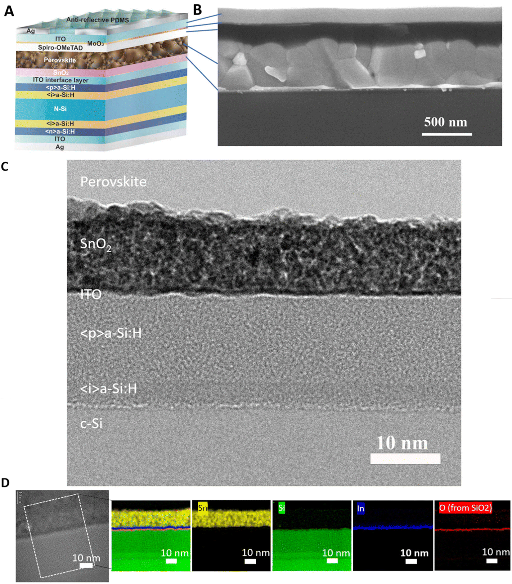 | ||
| Fig. 1 Schematic illustration of the monolithic perovskite/Si tandem solar cell and characterisation of the SnO2/ultra-thin ITO interface. (A) Schematic of the perovskite–silicon tandem cell structure. (B) Cross-sectional scanning electron microscopy (SEM) image of a typical perovskite top cell in the tandem device. (C) Bright field transmission electron microscopy (TEM), showing the interfacing layers with different crystallinities, including the underlying crystalline Si wafer surface. (D) Cross-sectional scanning transmission electron microscopy (STEM) and the corresponding electron energy loss spectroscopy (EELS) maps of Sn, Si, In and O, allowing the SnO2/ITO/native SiO2/〈p〉a-Si:H structure to be resolved (spectrum image of this region and the corresponding EELS spectra can be found in Fig. S2, ESI†). | ||
To investigate the effect of the ITO thickness on the tandem cell performance, we fixed the thickness of the 〈p〉a-Si:H in the Si bottom cells at 13 nm35 and we fabricated 1 cm2 tandem test cells with ultra-thin (≤5 nm) ITO layers at 5 different thicknesses. These test cells have identical structures as shown in Fig. 1A except that they did not have antireflective PDMS layers. The J–V curves of the champion testing tandem devices with different ITO interlayer thickness are shown in Fig. 2A. Their respective Suns-VOC curves are shown in Fig. S6 (ESI†) to determine the trend of series resistance (RS) and pseudo-FF (pFF) of tandem solar cells with varying interlayer ITO thicknesses (Table 1). The distribution of the electrical characteristics of the test cells is shown in Fig. 2B–D and is summarised in Table 1. JSC remained constant as the ITO thickness varied, in agreement with optical simulation (Fig. S7, ESI†). VOC and especially FF were the highest when the ITO was 1.7 nm thick, maximizing PCE but decreased when the ITO thickness was increased or reduced further (e.g., >1.7 nm or <1.7 nm). With respect to RS, the devices followed a similar trend to the FF while the RSH decreased with the ITO thickness (Fig. S8, ESI†).
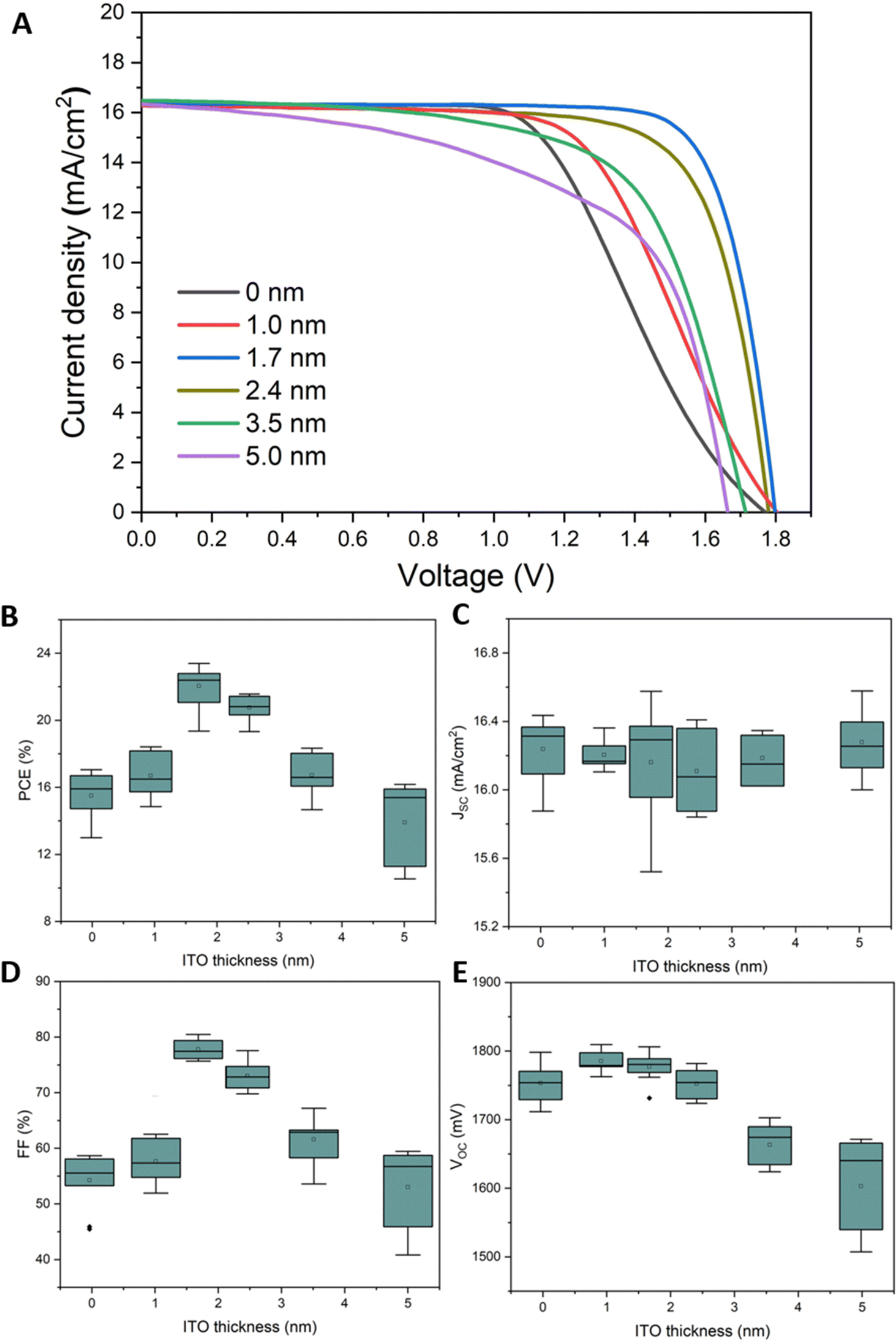 | ||
| Fig. 2 Effect of the ITO inter-layer thickness on the performance of 1 cm2 tandem test solar cells prior to the application of front anti-reflection control. (A) J–V curve of the champion testing tandem devices with different ITO interlayer thicknesses. Distribution of (B) PCE, (C) short-circuit current density (JSC), (D) fill factor (FF), and (E) open circuit voltage (VOC) based on 10 devices for each condition. The highest value is the maximum value. The highest bar is the 75th percentile value. The middle bar is the median value. The square mark is for the average. The lowest bar is the 25th percentile value. The lowest value is the minimum. | ||
| ITO (nm) | PCE (%) | V OC (mV) | J SC (mA cm−2) | FF (%) | R S (mΩ cm2) | R SH (Ω cm2) | R S, Suns-Voc (Ω cm2) | Pff (%) |
|---|---|---|---|---|---|---|---|---|
| 0 | 15.5 ± 2.5 | 1758 ± 45 | 16.2 ± 0.4 | 52.0 ± 6.0 | 60 ± 10 | 6251 ± 1841 | 5.33 | 84.3 |
| 1.0 | 16.7 ± 1.7 | 1787 ± 33 | 16.1 ± 0.2 | 56.2 ± 5.2 | 35 ± 5 | 5820 ± 2630 | 5.59 | 83.8 |
| 1.7 | 22.1 ± 2.4 | 1775 ± 37 | 16.2 ± 0.6 | 77.6 ± 3.0 | 7 ± 3 | 3962 ± 937 | 0.82 | 84.4 |
| 2.4 | 20.8 ± 1.3 | 1753 ± 42 | 16.1 ± 0.3 | 73.4 ± 4.6 | 9 ± 4 | 3749 ± 686 | 0.89 | 84.0 |
| 3.5 | 16.8 ± 2.1 | 1663 ± 39 | 16.1 ± 0.2 | 61.2 ± 7.8 | 21 ± 10 | 1840 ± 750 | 3.26 | 70.4 |
| 5.0 | 13.9 ± 2.4 | 1603 ± 94 | 16.2 ± 0.3 | 53.5 ± 11.2 | 25 ± 8 | 1127 ± 411 | 8.61 | 65.8 |
The decrease in RSH with ITO thickness was due to the improved lateral conductivity in the ITO layers failing to localise shunting effects. The improved lateral conductivity was confirmed by sheet resistance measurements (Fig. S9A, ESI†) and the evidence of increased shunting could be seen by the appearance of the humps in the lower voltage region of the dark current–voltage (IV) characteristics of the tandem devices with 3.5 nm and 5 nm ITO as shown in Fig. S10 (ESI†). The number of shunted and low-VOC cells also increase with 3.5 nm and 5 nm ITO (Fig. S11, ESI†) thereby lowering the mean VOC values observed in Fig. 2 and Table 1. It is important to note that the function of ultra-thin ITO localising shunts is effective in cells with areas ≥1 cm2 (i.e., commercially relevant cells) and is not obvious in small cells. To verify this, we fabricated small (0.09 cm2) perovskite–Si tandem devices with 5 nm or 20 nm ITO interlayers. The results in Fig. S12 (ESI†) show much less sensitivity to ITO interlayer thickness and higher efficiencies (23.5% for the champion cell with a 5 nm ITO interlayer and 23.0% for the champion cell with a 20 nm ITO interlayer) could be achieved due to shunting being less severe but only on a very small area e.g., 0.09 cm2.
In terms of RS, it is at its minimum in the case of 1.7 nm ITO layer, as the continuous film had sufficient conductivity for carrier transport in the vertical direction (Fig. S9B, ESI†). For both 1 nm and 0 nm ITO cases, RS was higher and an “S-shape” could be observed in the light JV curves (Fig. 2A). The higher RS for the 1 nm ITO case can be explained by the discontinuous film (Fig. S4 and S5, ESI†). To investigate the cause of the “S-shape”, Sentaurus technology computer-aided design (TCAD) was used to model the energy band structure of the tandem cells under thermal equilibrium with and without ITO. The results are shown in Fig. 3. In the presence of a continuous ITO film as in the case of 1.7 nm ITO, due to the high trap density of ITO, the ultra-thin layers provide sufficient trap states for the interface between the ITO layer and the 〈p〉a-Si:H layer via trap assisted tunnelling.36,37 In the case of 1 nm and 0 nm ITO layers, the SnO2 layer is in direct contact with the 〈p〉a-Si:H locally or over the full area, and the low trap density state provided by the SnO2 layer is not sufficient for holes tunnelling from the 〈p〉a-Si:H layer and electrons recombining in SnO2 thereby exhibiting the “S-shape” JV characteristic as observed. In terms of the effect of the 1.5 nm native SiO2 layer (as observed in Fig. 1D and Fig. S2, ESI†), trap assisted tunnelling is still feasible as shown in the simulated band diagram in Fig. S13 (ESI†).
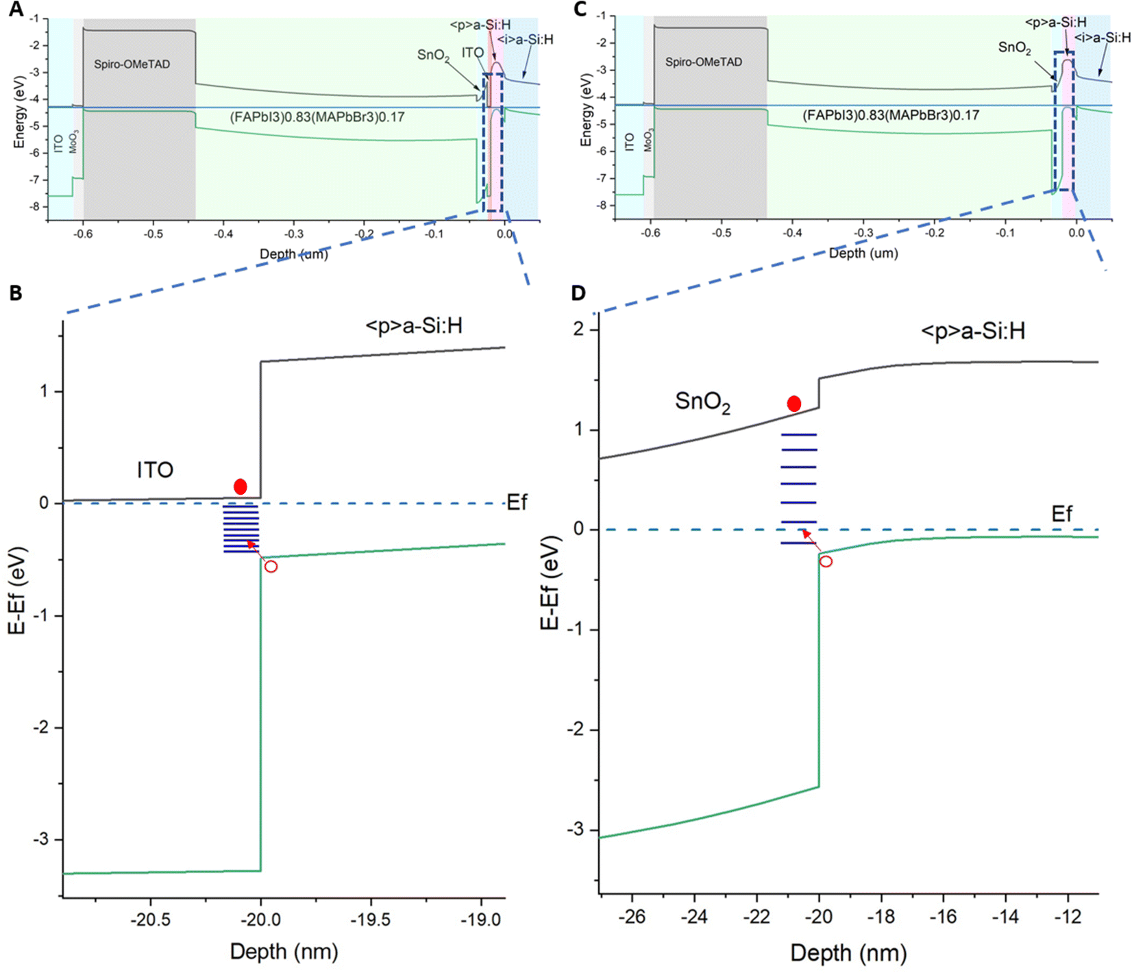 | ||
| Fig. 3 Simulated energy band structure of the tandem device under thermal equilibrium. Simulated band diagram of the full tandem device (A and B) with and (C and D) without ITO interface layers at equilibrium. (B) Zoomed-in view of (A) highlighting the ITO/〈p〉a-Si:H recombination stack. (D) Zoomed-in view of (C) highlighting the SnO2/〈p〉a-Si:H recombination stack. Solid and hollow red dots denote electrons and holes, respectively. | ||
To investigate the effect of ITO deposition, and ITO/SnO2/perovskite stack deposition with varying ITO thicknesses on Si-surface passivation, and recombination, we carried out (i) photoluminescence (PL) imaging, and (ii) carrier lifetime, dark saturation current density and implied VOC measurements on silicon half cells (front metallization not completed) before ITO deposition, after ITO deposition and after ITO/SnO2/perovskite deposition.
Comparison of Si half cells before and after ITO deposition shows negligible changes in the photoluminescence intensity (Fig. S14, ESI†), carrier lifetime (Fig. S15A, ESI†) and implied VOC (Fig. S15B and Table S4, ESI†) indicating that cells did not experience “sputter damage” from ITO deposition.
There were also negligible changes in the photoluminescence intensity (Fig. S14, ESI†), carrier lifetime (values remain in the same order of magnitude) (Fig. S15A, ESI†) and implied VOC (Fig. S15B and Table S4, ESI†) of the Si half cells after the deposition of the ITO/SnO2/perovskite, as SnO2 deposition required UV-ozone treatment prior to the ITO deposition. This indicates that the interfacing fabrication processes did not have a detrimental effect on the surface passivation quality of the Si half cells.
The effect of varying the interlayer ITO thickness on Si front-surface passivation was also negligible, with insignificant changes in photoluminescence intensities (Fig. S14, ESI†), carrier lifetimes (Fig. S15A, ESI†), implied VOC (Fig. S15B and Table S4, ESI†) and dark saturation current density J0 (values remain in the same order of magnitude) (Table S5, ESI†). All of these indicate no change in the dominant recombination mechanism,38 consistent with the shape of the injection independent lifetime curves remaining similar for Si cells with different ITO thicknesses (Fig. S16, ESI†).
It was found that our ITO is more conductive (Table S2, ESI†) than those typically used in SHJ solar cells.39 For example, the resistivity of our ITO at 100 nm is 4.28 × 10⁻⁴ Ω cm (RSH=42.8 Ω per square) while for ITO normally used in a SHJ solar cell, the resistivity is around 1.61 × 10⁻³ Ω cm for a 70 nm thick layer (RSH = 230 Ω per square).39 This can result in the formation a strong Schottky contact between the ITO and 〈p〉a-Si:H layers leading to a depletion of charge carriers in the 〈p〉a-Si:H and therefore a reduction in the built-in potential.40 This needs to be compensated by the increase in the thickness of the 〈p〉a-Si:H junction to increase the built-in potential back to desired levels.41,42 This was experimentally confirmed by comparing representative silicon bottom cells with a 13 nm thick or 26 nm thick 〈p〉a-Si:H layer as shown in Fig. S17 (ESI†). As expected, the cell with a 26 nm thick 〈p〉a-Si:H produced higher VOC and FF but lower JSC due to higher parasitic short-wavelength absorption in the 26 nm thick 〈p〉a-Si:H junction compared to the 13 nm thick 〈p〉a-Si:H counterpart (Fig. S17C, ESI†). Tandem cell efficiency also improved when the 26 nm thick 〈p〉a-Si:H layer junction was used (with an ITO interlayer fixed at 1.7 nm) as shown in Fig. S18 (ESI†) due to improvements in VOC and FF. The thicker 〈p〉a-Si:H layer junction no longer has an effect on tandem JSC as short wavelength light is absorbed by the perovskite top cell while long wavelength light is absorbed deep in the bulk of the Si bottom cell. We then investigated the effect of varying the ITO interface layer thickness (0 nm, 1.0 nm, 1.7 nm, 2.4 nm, 3.5 nm and 5.0 nm) on the performance of tandem cells with a 26 nm 〈p〉a-Si: H junction. The result shows a similar trend to the cells with a thinner junction (Fig. S19, ESI†). That is, the optimum ITO interlayer thickness remained at 1.7 nm for the best power conversion efficiency.
After the application of the anti-reflection layer, we were able to demonstrate a 1 cm2 tandem device (Fig. 4A and B) with a JSC of 18.1 mA cm−2, a VOC of 1.82 V, and a high FF of 82.4% under reverse scan and a steady state PCE of 27.0%. with negligible hysteresis (Table 2). The PCE achieved is the highest for a n-i-p based perovskite/Si tandem solar cell demonstrating the effectiveness of this ultra-thin ITO interlayer design.
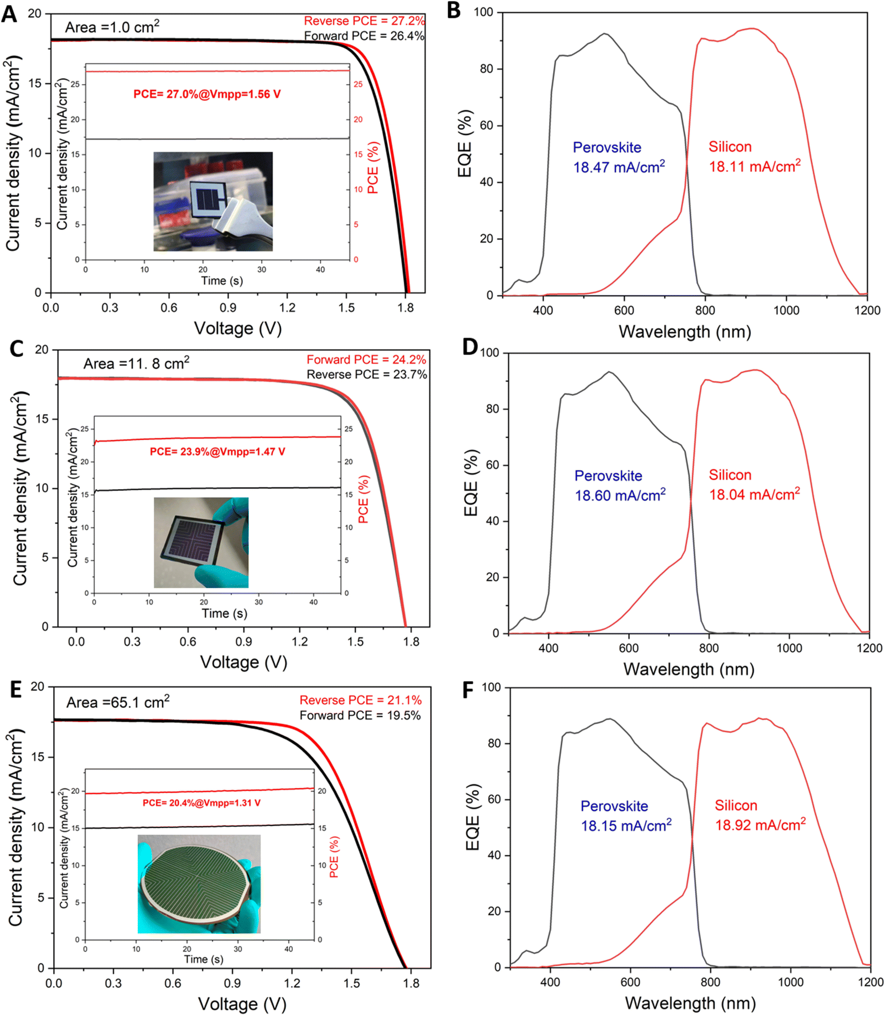 | ||
| Fig. 4 Performance of champion tandem devices of different sizes. (A, C and E) light J–V and (B, D and F) external quantum efficiency (EQE) of the perovskite-Si tandem devices of (A and B) 1 cm2, (C and D) 11.8 cm2, and (E and F) 65.1 cm2. Insets show the photographs of the fabricated tandem devices and their steady-state current densities and steady-state PCEs at fixed voltages near their maximum power points. | ||
| Area (cm2) | Scan | V OC (mV) | J SC (mA cm−2) | FF (%) | PCE (%) |
|---|---|---|---|---|---|
| 1.0 | Reverse | 1819 | 18.1 | 82.4 | 27.2 |
| Forward | 1804 | 18.1 | 80.6 | 26.4 | |
| 11.8 | Reverse | 1771 | 18.0 | 76.0 | 24.2 |
| Forward | 1770 | 17.9 | 74.5 | 23.7 | |
| 65.1 | Reverse | 1777 | 17.6 | 67.5 | 21.1 |
| Forward | 1772 | 17.7 | 62.3 | 19.5 |
To demonstrate the scalability of our ultra-thin interface using ultra-thin ITO layers to large area, 11.8 cm2 and 65.1 cm2 cells were also demonstrated achieving efficiencies of 24.2% and 21.1%, respectively. The J–V and EQE curves of the champion cells are shown in Fig. 4. Their parameters are listed in Table 2. The 65.1 cm2 tandem device produced a better infrared response due to the use of rear-textured cells while for the 1.0 and 11.8 cm2 tandem devices, rear polished silicon cells were used purely due to the cell availabilities at the time of demonstrations. A video showing an encapsulated 4-inch size tandem cell at work powering a “mini-wind-turbine” can be found in the ESI.† Performance drop in larger tandems was mainly caused by a decrease in FF. Reasons for higher hysteresis observed in larger tandem cells will need to be elucidated in future work. In terms of further JSC improvements, simulated EQE spectra in Fig. S20A (ESI†) show that this can be done firstly by matching the current between the top and bottom cells increasing JSC to around 18.7 mA cm−2. After that major losses limiting JSC shown in the pie chart in Fig. S20B (ESI†) need to be mitigated. They include front reflected and escaped losses as being the dominant (due to Fresnel reflection losses from refractive index mismatch between the top PDMS layer and the ITO/MoO3/Spiro-OMeTAD stack) loss followed by parasitic absorptions in the sun-facing Spiro-OMeTAD/MoO3 stack. Loss reduction can be achieved by replacing the stack with less absorbing materials43,44 or switching to p–i–n configuration as shown in Fig. S20C and S20D (ESI†) thereby increasing JSC towards 20 mA cm−2 for achieving a PCE of over 30%. In addition, efficiencies of large area cells can be further improved as metallisation and the fabrication of the perovskite layer continue to be optimised over large area to improve current and FF outputs.
The stability of an encapsulated tandem cell (Fig. S21, ESI†) was also tested under 1-sun continuous illumination with maximum power point (MPP) tracking. Encapsulation and testing details can be found in the ESI.† The results (Fig. 5) show that the tandem cell can maintain 98% of its initial performance after 600 hours demonstrating excellent light stability of the device structure. Preliminary 60 °C testing in N2 for 210 hours also shows reasonable thermal stability of the un-encapsulated tandem cell as shown in Fig. S22 (ESI†).
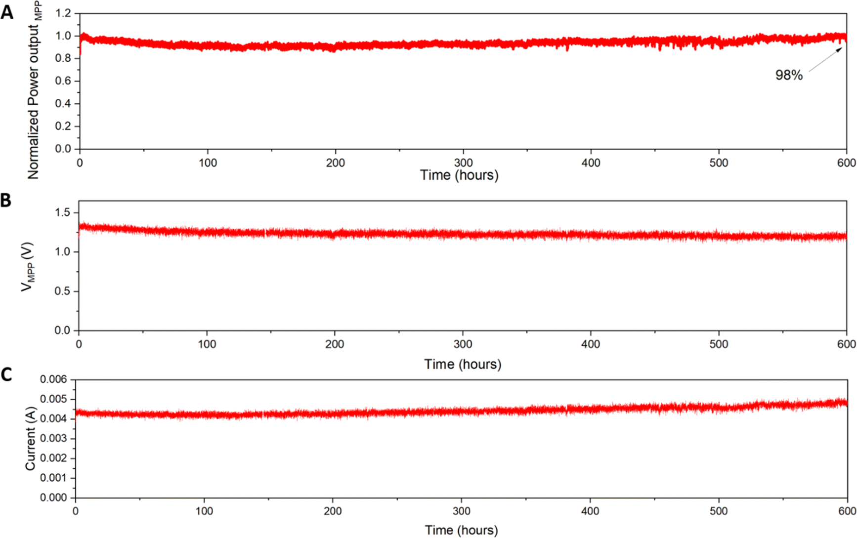 | ||
| Fig. 5 Stability testing of encapsulated 1 cm2 perovskite-Si tandem cells under continuous illumination (100 mW cm−2) at relative humidity of 60 ± 20% at room temperature. Maximum power point tracking of (A) power output, (B) voltage (VMPP) at the maximum power point and (C) current to the starting value at the maximum power. | ||
In conclusion, we have demonstrated the use of ultra-thin interface design for tandem solar cells with improved performance due to the reduction in parasitic resistance. As we are able to demonstrate perovskite–Si tandem devices with finer thickness resolution (e.g., 0.5 nm), it may be possible in future work to observe non-linear behaviour which would likely to occur45 with ultra-thin ITO interface layers when their thickness is varied at finer scale. In this work, a high fill factor (82.4% under reverse scan) was achieved using an interfacing ITO layer as thin as 1.7 nm. This value exceeds those reported thus far for perovskite–Si tandem devices. Power conversion efficiencies of 27.2%, 24.2% and 21.1% were achieved on 1.0 cm2, 11.8 cm2 on 65.1 cm2, respectively, under reverse scan. The cell structure developed also shows respectable stability with negligible efficiency loss after 600 hours of continuous 1 sun illumination at ambient temperature. This work has provided an elegant approach for optimizing interfacing for tandem solar cells. This is successfully demonstrated in this work with the integration of perovskite and Si solar cells for achieving large area monolithic tandem devices.
Author contributions
J. Z. and A. H.-B. conceived the project. W. D., A. L. and K. D. fabricated the Si bottom cells. J. Z. integrated perovskites onto Si bottom cells and completed the monolithic tandem cell fabrication. J. Z. conducted device characterization. W. D. and K. C. F. assisted with silicon bottom cell analysis. Z. C. Z., Y. G., F. M. and D. R. M. carried out the device simulation. H. Y., S. T., J. B. and C. X. conducted film characterization. L. G. and M. J. assisted with tandem stability testing. J. Q., L. Y. and J. M. C. conducted the STEM and EELS measurements and the associated analysis. H. Y. and A. U. assisted with the MoO3 layer deposition. C. Y., Y. Z., and S. B. assisted with the Suns-VOC and lifetime measurements for silicon bottom cells. A. H.-B., and D. R. M. supervised the research. J. Z. and A. H.-B. wrote the manuscript, and all authors were involved in the discussion of the results.Data and materials availability
All data needed to evaluate the conclusions in the paper are present in the paper or the ESI.† All the data are available from the corresponding authors upon reasonable request.Conflicts of interest
The authors declare that they have no competing interests.Acknowledgements
This work is supported by the Australian Government through the Australian Renewable Energy Agency (ARENA) via projects 2020 RND001 and 2020 RND003. J. Z. acknowledges the support from Australian Centre for Advanced Photovoltaics (ACAP) Postdoctoral Fellowships (RG123662-M). L. G., S. T. and C. L. acknowledge the support from the John Hooke Chair of Nanoscience Postgraduate Research Scholarships. G. W. acknowledges the support from University of Sydney International Stipend Scholarship (USydIS). A. H.-B. and J.M.C are supported by the Australian Research Council (ARC) Future Fellowships FT210100210 and FT180100232, respectively. M. J. acknowledges the support from Slovenian Research Agency (Javna agencija za raziskovalno dejavnost Republike Slovenije, ARRS) under the research program P2-0415. The authors acknowledge the technical and scientific assistance provided by (i) Sydney Microscopy & Microanalysis, the University of Sydney node of Microscopy Australia, (ii) the facilities as well as the scientific and technical assistance of the Research & Prototype Foundry Core Research Facility at the University of Sydney, part of the Australian National Fabrication Facility, (iii) Electron Microscopy Unit at UNSW and (iv) BioMedical Imaging Facility at UNSW.References
- M. A. Green, Commercial progress and challenges for photovoltaics, Nat. Energy, 2016, 1, 15015 CrossRef.
- K. Yoshikawa, H. Kawasaki, W. Yoshida, T. Irie, K. Konishi, K. Nakano, T. Uto, D. Adachi, M. Kanematsu and H. Uzu, Silicon heterojunction solar cell with interdigitated back contacts for a photoconversion efficiency over 26%, Nat. Energy, 2017, 2, 17032 CrossRef CAS.
- A. Richter, M. Hermle and S. W. Glunz, Reassessment of the limiting efficiency for crystalline silicon solar cells, IEEE J. photovoltaics, 2013, 3, 1184–1191 Search PubMed.
- NREL, https://www.nrel.gov/pv/cell-efficiency.html (Accessed January 11, 2023).
- A. W. Y. Ho-Baillie, J. Zheng, M. A. Mahmud, F.-J. Ma, D. R. McKenzie and M. Green, Recent progress and future prospects of perovskite tandem solar cells, Appl. Phys. Rev., 2021, 8, 041307 CAS.
- J. P. Mailoa, C. D. Bailie, E. C. Johlin, E. T. Hoke, A. J. Akey, W. H. Nguyen, M. D. McGehee and T. Buonassisi, A 2-terminal perovskite/silicon multijunction solar cell enabled by a silicon tunnel junction, Appl. Phys. Lett., 2015, 106, 121105 CrossRef.
- F. Sahli, B. A. Kamino, J. Werner, M. Bräuninger, B. Paviet-Salomon, L. Barraud, R. Monnard, J. P. Seif, A. Tomasi, Q. Jeangros, A. Hessler-Wyser, S. De Wolf, M. Despeisse, S. Nicolay, B. Niesen and C. Ballif, Improved Optics in Monolithic Perovskite/Silicon Tandem Solar Cells with a Nanocrystalline Silicon Recombination Junction, Adv. Energy Mater., 2018, 8, 1701609 CrossRef.
- J. Zheng, H. Mehrvarz, F.-J. Ma, C. F. J. Lau, M. A. Green, S. Huang and A. W. Y. Ho-Baillie, 21.8% Efficient Monolithic Perovskite/Homo-Junction-Silicon Tandem Solar Cell on 16 cm2, ACS Energy Lett., 2018, 3, 2299–2300 CrossRef CAS.
- B. Kamino, B. Paviet-Salomon, S.-J. Moon, N. Badel, J. Levrat, G. Christmann, A. Walter, A. Faes, L. Ding, J. J. Diaz Leon, A. Paracchino, M. Despeisse, C. Ballif and S. Nicolay, Low Temperature Screen-Print Metallization for the Scale Up of 2-Terminal Perovskite-Silicon Tandems, ACS Appl. Energy Mater., 2019, 2, 3815–3821 CrossRef CAS.
- CSEM Scientific and Technical Report 2019, https://www.csem.ch/pdf/128428?name=CSEM-STR-2019-p69.pdf.
- M. A. Green, E. D. Dunlop, J. Hohl-Ebinger, M. Yoshita, N. Kopidakis, K. Bothe, D. Hinken, M. Rauer and X. Hao, Solar cell efficiency tables (Version 60), Prog. Photovoltaics, 2022, 30, 687–701 Search PubMed.
- S. Albrecht, M. Saliba, J. P. Correa Baena, F. Lang, L. Kegelmann, M. Mews, L. Steier, A. Abate, J. Rappich, L. Korte, R. Schlatmann, M. K. Nazeeruddin, A. Hagfeldt, M. Grätzel and B. Rech, Monolithic perovskite/silicon-heterojunction tandem solar cells processed at low temperature, Energy Environ. Sci., 2016, 9, 81–88 RSC.
- J. Werner, C. H. Weng, A. Walter, L. Fesquet, J. P. Seif, S. De Wolf, B. Niesen and C. Ballif, Efficient Monolithic Perovskite/Silicon Tandem Solar Cell with Cell Area >1 cm(2), J. Phys. Chem. Lett., 2016, 7, 161–166 CrossRef CAS PubMed.
- K. A. Bush, A. F. Palmstrom, Z. J. Yu, M. Boccard, R. Cheacharoen, J. P. Mailoa, D. P. McMeekin, R. L. Z. Hoye, C. D. Bailie, T. Leijtens, I. M. Peters, M. C. Minichetti, N. Rolston, R. Prasanna, S. Sofia, D. Harwood, W. Ma, F. Moghadam, H. J. Snaith, T. Buonassisi, Z. C. Holman, S. F. Bent and M. D. McGehee, 23.6%-efficient monolithic perovskite/silicon tandem solar cells with improved stability, Nat. Energy, 2017, 2, 17009 CrossRef CAS.
- Y. Wu, D. Yan, J. Peng, T. Duong, Y. Wan, P. Phang, H. Shen, N. Wu, C. Barugkin, X. Fu, S. Surve, D. Walter, T. White, K. Catchpole and K. Weber, Monolithic perovskite/silicon-homojunction tandem solar cell with over 22% efficiency, Energy Environ. Sci., 2017, 10, 2472–2479 RSC.
- R. Fan, N. Zhou, L. Zhang, R. Yang, Y. Meng, L. Li, T. Guo, Y. Chen, Z. Xu, G. Zheng, Y. Huang, L. Li, L. Qin, X. Qiu, Q. Chen and H. Zhou, Toward Full Solution Processed Perovskite/Si Monolithic Tandem Solar Device With PCE Exceeding 20%, Solar RRL, 2017, 1, 1700149 CrossRef.
- K. A. Bush, S. Manzoor, K. Frohna, Z. J. Yu, J. A. Raiford, A. F. Palmstrom, H.-P. Wang, R. Prasanna, S. F. Bent, Z. C. Holman and M. D. McGehee, Minimizing Current and Voltage Losses to Reach 25%-Efficient Monolithic Two-Terminal Perovskite-Silicon Tandem Solar Cells, ACS Energy Lett., 2018, 3, 2173–2180 CrossRef CAS.
- S. Zhu, F. Hou, W. Huang, X. Yao, B. Shi, Q. Ren, J. Chen, L. Yan, S. An, Z. Zhou, H. Ren, C. Wei, Q. Huang, Y. Li, G. Hou, X. Chen, Y. Ding, G. Wang, B. Li, Y. Zhao and X. Zhang, Solvent Engineering to Balance Light Absorbance and Transmittance in Perovskite for Tandem Solar Cells, Solar RRL, 2018, 2, 1800176 CrossRef.
- Z. Qiu, Z. Xu, N. Li, N. Zhou, Y. Chen, X. Wan, J. Liu, N. Li, X. Hao, P. Bi, Q. Chen, B. Cao and H. Zhou, Monolithic perovskite/Si tandem solar cells exceeding 22% efficiency via optimizing top cell absorber, Nano Energy, 2018, 53, 798–807 CrossRef CAS.
- B. Chen, Z. Yu, K. Liu, X. Zheng, Y. Liu, J. Shi, D. Spronk, P. N. Rudd, Z. Holman and J. Huang, Grain Engineering for Perovskite/Silicon Monolithic Tandem Solar Cells with Efficiency of 25.4%, Joule, 2019, 3, 177–190 CrossRef CAS.
- M. Jošt, E. Köhnen, A. Morales Vilches, B. Lipovšek, K. Jäger, B. Macco, A. Al-Ashouri, J. Krc, L. Korte, B. Rech, R. Schlatmann, M. Topic, B. Stannowski and S. Albrecht, Textured interfaces in monolithic perovskite/silicon tandem solar cells: Advanced light management for improved efficiency and energy yield, Energy Environ. Sci., 2018, 11, 3511–3523 RSC.
- F. Hou, C. Han, O. Isabella, L. Yan, B. Shi, J. Chen, S. An, Z. Zhou, W. Huang, H. Ren, Q. Huang, G. Hou, X. Chen, Y. Li, Y. Ding, G. Wang, C. Wei, D. Zhang, M. Zeman, Y. Zhao and X. Zhang, Inverted pyramidally-textured PDMS antireflective foils for perovskite/silicon tandem solar cells with flat top cell, Nano Energy, 2019, 56, 234–240 CrossRef CAS.
- F. Hou, L. Yan, B. Shi, J. Chen, S. Zhu, Q. Ren, S. An, Z. Zhou, H. Ren, C. Wei, Q. Huang, G. Hou, X. Chen, Y. Li, Y. Ding, G. Wang, D. Zhang, Y. Zhao and X. Zhang, Monolithic Perovskite/Silicon-Heterojunction Tandem Solar Cells with Open-Circuit Voltage of over 1.8 V, ACS Appl. Energy Mater., 2019, 2, 243–249 CrossRef CAS.
- L. Mazzarella, Y.-H. Lin, S. Kirner, A. B. Morales-Vilches, L. Korte, S. Albrecht, E. Crossland, B. Stannowski, C. Case, H. J. Snaith and R. Schlatmann, Infrared Light Management Using a Nanocrystalline Silicon Oxide Interlayer in Monolithic Perovskite/Silicon Heterojunction Tandem Solar Cells with Efficiency above 25%, Adv. Energy Mater., 2019, 9, 1803241 CrossRef.
- C. U. Kim, J. C. Yu, E. D. Jung, I. Y. Choi, W. Park, H. Lee, I. Kim, D.-K. Lee, K. K. Hong and M. H. Song, Optimization of device design for low cost and high efficiency planar monolithic perovskite/silicon tandem solar cells, Nano Energy, 2019, 60, 213–221 CrossRef CAS.
- E. Köhnen, M. Jošt, A. B. Morales-Vilches, P. Tockhorn, A. Al-Ashouri, B. Macco, L. Kegelmann, L. Korte, B. Rech, R. Schlatmann, B. Stannowski and S. Albrecht, Highly efficient monolithic perovskite silicon tandem solar cells: analyzing the influence of current mismatch on device performance, Sustainable Energy Fuels, 2019, 3, 1995–2005 RSC.
- A. J. Bett, P. S. C. Schulze, K. M. Winkler, Ö. S. Kabakli, I. Ketterer, L. E. Mundt, S. K. Reichmuth, G. Siefer, L. Cojocaru, L. Tutsch, M. Bivour, M. Hermle, S. W. Glunz and J. C. Goldschmidt, Two-terminal Perovskite silicon tandem solar cells with a high-Bandgap Perovskite absorber enabling voltages over 1.8 V, Prog. Photovoltaics, 2019, 28, 99–110 Search PubMed.
- B. Chen, Z. J. Yu, S. Manzoor, S. Wang, W. Weigand, Z. Yu, G. Yang, Z. Ni, X. Dai, Z. C. Holman and J. Huang, Blade-Coated Perovskites on Textured Silicon for 26%-Efficient Monolithic Perovskite/Silicon Tandem Solar Cells, Joule, 2020, 4, 850–864 CrossRef CAS.
- J. Xu, C. C. Boyd, J. Y. Zhengshan, A. F. Palmstrom, D. J. Witter, B. W. Larson, R. M. France, J. Werner, S. P. Harvey and E. J. Wolf, Triple-halide wide–band gap perovskites with suppressed phase segregation for efficient tandems, Science, 2020, 367, 1097–1104 CrossRef CAS PubMed.
- D. Kim, H. J. Jung, I. J. Park, B. W. Larson, S. P. Dunfield, C. Xiao, J. Kim, J. Tong, P. Boonmongkolras, S. G. Ji, F. Zhang, S. R. Pae, M. Kim, S. B. Kang, V. Dravid, J. J. Berry, J. Y. Kim, K. Zhu, D. H. Kim and B. Shin, Efficient, stable silicon tandem cells enabled by anion-engineered wide-bandgap perovskites, Science, 2020, 368, 155–160 CrossRef CAS PubMed.
- P. S. C. Schulze, A. J. Bett, M. Bivour, P. Caprioglio, F. M. Gerspacher, Ö. Ş. Kabaklı, A. Richter, M. Stolterfoht, Q. Zhang, D. Neher, M. Hermle, H. Hillebrecht, S. W. Glunz and J. C. Goldschmidt, 25.1% High-Efficient Monolithic Perovskite Silicon Tandem Solar Cell with a High Band Gap Perovskite Absorber, Solar RRL, 2020, 4, 2000152 CrossRef CAS.
- A. S. Subbiah, F. H. Isikgor, C. T. Howells, M. De Bastiani, J. Liu, E. Aydin, F. Furlan, T. G. Allen, F. Xu, S. Zhumagali, S. Hoogland, E. H. Sargent, I. McCulloch and S. De Wolf, High-Performance Perovskite Single-Junction and Textured Perovskite/Silicon Tandem Solar Cells via Slot-Die-Coating, ACS Energy Lett., 2020, 5, 3034–3040 CrossRef CAS.
- A. Al-Ashouri, E. Köhnen, B. Li, A. Magomedov, H. Hempel, P. Caprioglio, J. A. Márquez, A. B. M. Vilches, E. Kasparavicius and J. A. Smith, Monolithic perovskite/silicon tandem solar cell with >29% efficiency by enhanced hole extraction, Science, 2020, 370, 1300–1309 CrossRef CAS PubMed.
- J. Zheng, H. Mehrvarz, C. Liao, J. Bing, X. Cui, Y. Li, V. R. Gonçales, C.-F. J. Lau, D. S. Lee, Y. Li, M. Zhang, J. Kim, Y. Cho, L. G. Caro, S. Tang, C. Chen, S. Huang and A. W. Y. Ho-Baillie, Large Area 23%-Efficient Monolithic Perovskite/Homo-Junction-Silicon Tandem Solar Cell With Enhanced UV Stability Using Down-Shifting Material, ACS Energy Lett., 2019, 4, 2623–2631 CrossRef CAS.
- W. Duan, A. Lambertz, K. Bittkau, D. Qiu, K. Qiu, U. Rau and K. Ding, A route towards high-efficiency silicon heterojunction solar cells, Prog. Photovoltaics, 2021, 30, 384–392 Search PubMed.
- M. De Bastiani, A. S. Subbiah, E. Aydin, F. H. Isikgor, T. G. Allen and S. De, Wolf, Recombination junctions for efficient monolithic perovskite-based tandem solar cells: physical principles, properties, processing and prospects, Mater. Horiz., 2020, 7, 2791–2809 RSC.
- C. Messmer, M. Bivour, J. Schön, S. W. Glunz and M. Hermle, Numerical simulation of silicon heterojunction solar cells featuring metal oxides as carrier-selective contacts, IEEE J. Photovoltaics, 2018, 8, 456–464 Search PubMed.
- S. Rein, Lifetime spectroscopy: a method of defect characterization in silicon for photovoltaic applications, Springer Science & Business Media, 2006 Search PubMed.
- Z. Yao, W. Duan, P. Steuter, J. Hüpkes, A. Lambertz, K. Bittkau, M. Pomaska, D. Qiu, K. Qiu, Z. Wu, H. Shen, U. Rau and K. Ding, Influence of Oxygen on Sputtered Titanium-Doped Indium Oxide Thin Films and Their Application in Silicon Heterojunction Solar Cells, Solar RRL, 2021, 5, 2000501 CrossRef CAS.
- M. Bivour, M. Reusch, S. Schroer, F. Feldmann, J. Temmler, H. Steinkemper and M. Hermle, Doped Layer Optimization for Silicon Heterojunctions by Injection-Level-Dependent Open-Circuit Voltage Measurements, IEEE J. Photovoltaics, 2014, 4, 566–574 Search PubMed.
- M. Rahmouni, A. Datta, P. Chatterjee, J. Damon-Lacoste, C. Ballif and P. Roca I Cabarrocas, Carrier transport and sensitivity issues in heterojunction with intrinsic thin layer solar cells on N-type crystalline silicon: A computer simulation study, J. Appl. Phys., 2010, 107, 054521 CrossRef.
- H. Fujiwara and M. Kondo, Effects of a-Si:H layer thicknesses on the performance of a-Si:H/c-Si heterojunction solar cells, J. Appl. Phys., 2007, 101, 054516 CrossRef.
- J. Zheng, C. F. J. Lau, H. Mehrvarz, F.-J. Ma, Y. Jiang, X. Deng, A. Soeriyadi, J. Kim, M. Zhang, L. Hu, X. Cui, D. S. Lee, J. Bing, Y. Cho, C. Chen, M. A. Green, S. Huang and A. W. Y. Ho-Baillie, Large area efficient interface layer free monolithic perovskite/homo-junction-silicon tandem solar cell with over 20% efficiency, Energy Environ. Sci., 2018, 11, 2432–2443 RSC.
- E. Aydin, J. Liu, E. Ugur, R. Azmi, G. T. Harrison, Y. Hou, B. Chen, S. Zhumagali, M. De Bastiani, M. Wang, W. Raja, T. G. Allen, A. U. Rehman, A. S. Subbiah, M. Babics, A. Babayigit, F. H. Isikgor, K. Wang, E. Van Kerschaver, L. Tsetseris, E. H. Sargent, F. Laquai and S. De Wolf, Ligand-bridged charge extraction and enhanced quantum efficiency enable efficient n–i–p perovskite/silicon tandem solar cells, Energy Environ. Sci., 2021, 14, 4377–4390 RSC.
- Z. C. Zhao and D. R. McKenzie, Antireflection coating of barriers to enhance electron tunnelling: exploring the matter wave analogy of superluminal optical phase velocity, Sci. Rep., 2017, 7, 12772 CrossRef PubMed.
Footnotes |
| † Electronic supplementary information (ESI) available. See DOI: https://doi.org/10.1039/d2ee04007g |
| ‡ These authors contributed equally to this work. |
| This journal is © The Royal Society of Chemistry 2023 |