
 Open Access Article
 This Open Access Article is licensed under a
 Creative Commons Attribution 3.0 Unported Licence
Deposition of a high entropy thin film by aerosol-assisted chemical vapor deposition†
Weichen
Xiao
 a,
Mark A.
Buckingham
a,
Yi
Li
a,
Kerry
Hazeldine
b,
Bing
Han
a,
Sarah H.
Cartmell
a,
Alexander S.
Eggeman
a,
Alex S.
Walton
b and
David J.
Lewis
*a
a,
Mark A.
Buckingham
a,
Yi
Li
a,
Kerry
Hazeldine
b,
Bing
Han
a,
Sarah H.
Cartmell
a,
Alexander S.
Eggeman
a,
Alex S.
Walton
b and
David J.
Lewis
*a
aDepartment of Materials, The University of Manchester, Manchester M13 9PL, UK. E-mail: david.lewis-4@manchester.ac.uk
bDepartment of Chemistry and the Photon Science Institute, The University of Manchester, Oxford Road, Manchester, M13 9PL, UK
First published on 27th September 2023
Abstract
Herein we report for the first time the synthesis of a high entropy (CuZnCoInGa)S metal sulfide thin film deposited by AACVD using molecular precursors.
High entropy (HE) materials are so called as they have an inherently high configurational entropy (ΔSconf).1,2 These materials were first reported as alloys, where the high ΔSconf arises from disorder in the lattice by containing a random arrangement of five or more elements.2 Subsequently, this area has greatly expanded into metal oxides,3 nitrides, carbides and borides, among others.4 The wide range of synthesised HE materials has led to an equally wide range of applications, including thermoelectric energy conversion,5 catalysis,6 energy storage,7 supercapacitors and solar absorbers in photovoltaic devices.8 HE chalcogenides are a recent development in this area, but have already shown great promise in energy conversion, storage, and catalysis, as highlighted in a recent review.9
HE metal chalcogenides are relatively underdeveloped due to synthetic barriers associated with their elemental complexity. To date, these procedures have required long timescales (up to 60 h),10 high temperatures (>1000 °C),11 and potentially hazardous synthetic techniques.12 HE metal sulfides have been synthesised as bulk,13 2D,12 and 0D nanomaterials14 and have shown promise for electrocatalysis,15 Li-ion batteries,13 and thermoelectrics.5 On the other hand, simple metal chalcogenide thin films are widely investigated and utilised in applications including thermoelectric, optoelectronic and biomedical applications.16 However, despite the rich array of potential applications where metal chalcogenide thin films excel, to the best of our knowledge there has been no reports of thin film HE metal sulfides, even though thin films, rather than particulate metal chalcogenides are a more technologically useful form of the material.
Aerosol-assisted chemical vapor deposition (AACVD) is an ambient pressure technique for the deposition of thin films.17–19 AACVD typically employs single source molecular precursors such as dithiocarbamates20 or dithiocarbonates21 and a carrier gas to transport a nebulised aerosol of precursors to either a hot-wall or cold-wall reactor that decomposes the precursors, depositing a thin film. It relies on aerosol droplets of soluble precursors, rather than evaporation of volatile precursors to deposit the film, increasing the range of possible precursors that can be used and materials that can be deposited. AACVD is also a scalable technique and has been proposed as potentially cost-effective compared to other deposition techniques owing to its inherent simplicity.22,23 The physical properties of deposited films such as particle size, morphology, film thickness, can also be controlled by the chemistry of selected precursors,21 along with the deposition temperature, time, solvent, carrier flow rate and frequency of the ultrasonic modulator.
Here we set out to investigate if it was possible to synthesise a HE metal sulfide (HEMS) thin film by exploiting the advantages of both AACVD (facile, ambient pressure), and single source precursors (rapid and low temperature decomposition) in tandem. The aim being to produce HEMS thin films.
In a typical AACVD experiment to produce a HEMS thin film (schematic shown in Fig. S1, ESI†), equimolar (0.1 mmol) amounts of each metal dithiocarbamate precursor (full details in ESI†) was dissolved in 10 mL of THF. A digital ultrasonic humidifier was then used to produce an aerosol, which was subsequently carried to the furnace (pre-heated to 550 °C) by flowing N2. The precursor cocktail decomposes to the HEMS thin film,15,24 depositing the material on glass substrates. Fig. 1(a) shows the diffraction pattern obtained from grazing incidence XRD (GIXRD) which matches approximately to chalcopyrite (ICSD: 66865). Rietveld refinement of the obtained powder X-ray diffraction pXRD was ultimately used to determine the lattice parameters of the thin film (Fig. S7, ESI†). It was found that the calculated lattice parameters (a = b = 5.47, Å c = 10.82 Å, α = β = γ = 90°) of our HE system are slightly smaller than that of a chalcopyrite (CuInS2, a = b = 5.52 Å, c = 11.09 Å, α = β = γ = 90°), which is likely caused by lattice distortion induced by the presence of smaller Co3+ and Ga3+ ions (values in Table S3, ESI†).25 The calculated parameters were further confirmed through HR-TEM analysis. As shown in Fig. 2(a) and (b), an inter planar spacing of 1.93 Å (1.93 nm between 11 layers) was observed, which likely corresponds to the (102) lattice plane (d102 = 1.93 Å, 2θ = 47.1°) which we observe in the pXRD pattern, but could be the (110) lattice plane, which has a very similar d-spacing. Cross-sectional SEM (Fig. 2(c)) confirmed a continuous thin film was deposited with ca. 1.5 μm thickness.
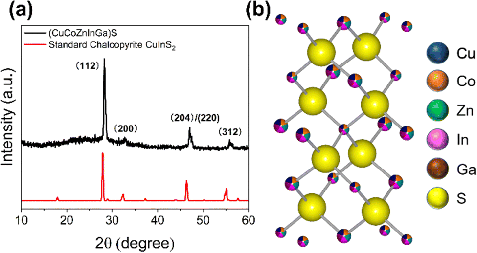 | ||
| Fig. 1 Figure of (a) powder X-ray diffraction pattern of thin film (CoCuZnGaIn)S with reference to standard chalcopyrite (CuInS2, ICSD: 66865). (b) The crystal structure of HE chalcopyrite (a = b = 5.52, c = 11.13, α = β = γ = 90°). | ||
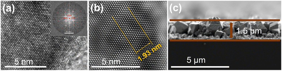 | ||
| Fig. 2 (a) High resolution TEM image of crystallites from the deposited film (inset: Fast Fourier transform (FFT) from (a), overlayed with a CuInS2 diffraction pattern simulated by single crystal in a (22−1) direction). (b) Inversed FFT from the FFT of (a) and measured lattice spacing corresponding to either the (102) or (110) lattice plane (the difference in d-spacing is <1%, both are presented in the FFT pattern). (c) Cross sectional SEM images of the deposited film and measured thickness. | ||
SEM imaging revealed a change in both particle size and morphology across the deposited film. The leading edge of the film (ca. 1–6.5 mm) was found to have a more flake-like morphology, which changed to a more cube-like morphology along the rest of the film. To both enable comparable quantitative analysis and demonstrate this change in morphology, the film was divided into 9 positions (position 1 closest to the furnace inlet to position 9 furthest away from the inlet), with each position representing ca. 2.2 mm on the film, Fig. S1(b) (ESI†). Fig. S10(a)–(i) (ESI†) shows the change in morphology from position 1 (a, ca. 1 mm into the substrate) to 9 (i, ca. 19 mm into the substrate). Quantitative particle size analysis in each position across the film was undertaken and found that there is a change in particle size with the initial 6 mm having an average size ca. 300 nm and the remaining 14 mm having an average size ca. 500–600 nm (Fig. 3(a) and Table S4, ESI†).
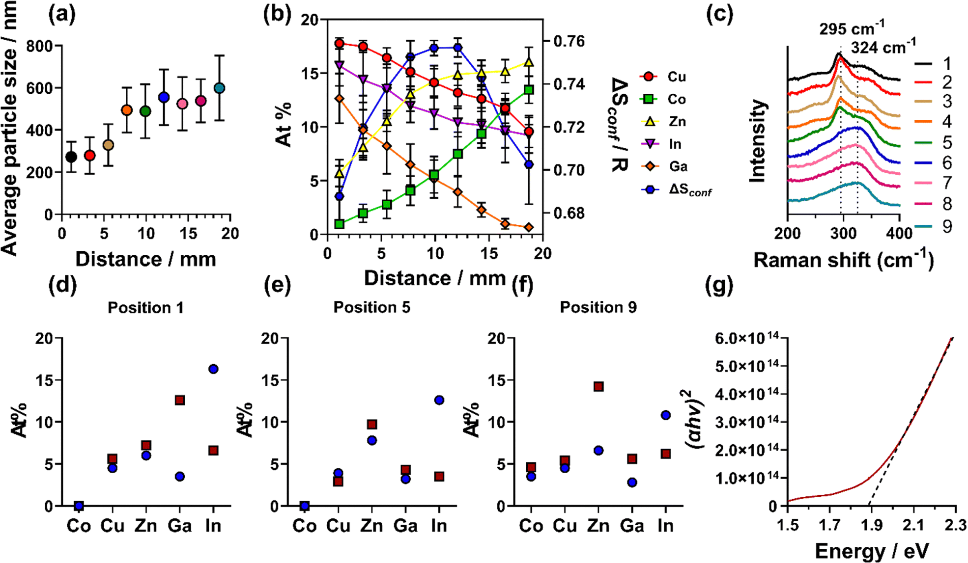 | ||
| Fig. 3 (a) Particle size distribution analysis across the film of the SEM images (Fig. S8, ESI†). (b) SEM-EDX elemental analysis across the film. (c) Raman spectra obtained across the film (d)–(f) XPS (blue circles) vs. HAXPES (red squares) atomic abundance determined from (d) the initial 1–3 mm, (e) 9–11 mm and (f) 17–20 mm of the film. (g) Tauc plot of the UV-Vis spectra shown in Fig. S23 (ESI†). | ||
Energy dispersive X-ray spectroscopic (EDX) mapping was also used in conjunction with SEM to investigate the spatial distribution of elements, by imaging the 9 positions across the film, encompassing its full 20 mm length. From each spectroscopic map, it was found that a homogeneous distribution of elements was observed (Fig. S11–S19, ESI†), consistent with the metals randomly arranged in the cation sub-lattice.9 In addition, elements are distributed homogeneously when cross sectional imaging is performed (Fig S26, ESI†). However, when comparing quantitative elemental composition across all positions (Fig. 3(b)), trends emerged. At the beginning of the film (up to ca. 6 mm), the elemental composition was found to be Cu, Ga, and In-rich and Co and Zn-poor. In the middle of the film (ca. 7–15 mm), a more homogeneous composition was observed and the rear of the film (the remaining ca. 5 mm) was found to be Ga-poor and Co and Zn-rich. As the elemental composition was found to change along the films, there is a subsequent change in ΔSconf, as shown by the blue hexagons in Fig. 3(b). This analysis showed that the entropy reaches a maximum in the middle of the deposited film, with a decrease in entropy at both the front (Co and Zn poor region) and rear (Ga poor region). This change in elemental composition and entropy along the film is caused by the thermal gradient of the furnace and varying decomposition temperatures of the precursors (vide infra).
To further analyse the thin film, Raman spectroscopy was employed, over equivalent positions to the SEM analysis across the entire film (also labelled as 1–9 in Fig. 3(c)). Two peaks were observed in the initial 11 mm of the film, with a sharp peak ca. 295 cm−1 and a broader shoulder ca. 343 cm−1. This is consistent with previous reports of Cu-rich chalcopyrite CuInS2, where the peak centred ca. 295 cm−1 was attributed to the A1 vibration of the S–S bonds.26,27 It has been reported that chalcopyrite CuInS2 can transform to a cubic zinc blende (ZB) structure when the atomic percentage of Cu is decreased to 15.5–11%.28 In our sample, from ca. 12 mm into the sample (position 6) the atomic percentage of Cu decreases from 16% at ca. 10 mm to 14.9% at ca. 12 mm. As noted, we also observed a more cubic-like morphology along the film (vide supra). This predicted change in structure is also observed by Raman analysis, where the sharp peak at 295 cm−1 is no longer present across the last 8 mm of the film. Here, there only remains a single, broad peak centred ca. 324 cm−1. The peak broadening can result from a small domain size confirmed by pXRD (37 ± 4 nm calculated from Rietveld Refinement). The breadth of the peak centred on 324 cm−1 decreased along the final 8 mm of the film, consistent with the domain size increasing, which we also observed by SEM (Fig. 3(a)). Due to the peak broadening, it was difficult to accurately assign this peak as there are many possible peaks overlapping in the range of 305–340 cm−1.27 Despite this, Raman analysis again supported our assignment of HES with the chalcopyrite structure.
We ascribe all these compositional and morphological changes to inhomogeneous furnace temperature; over the 20 mm distance of the substrate within the furnace, there was found to be an around 90 °C increase in temperature away from the inlet of the hot wall reactor (ca. 340 vs. 430 °C) measured using a thermocouple. The thermogravimetric analysis (TGA) plots of the precursors are shown in Fig. S4 (ESI†). These show that Cu, Zn, and Ga dithiocarbamates have similar low deposition onset temperatures of ca. 248 °C, 241 °C and 254 °C (see TGA data in Fig. S4, ESI†). Co dithiocarbamate has a slightly higher deposition onset temperature of 266 °C, with In dithiocarbamate having a high onset decomposition temperature of 310 °C. The decomposition (and therefore deposition) window, which is the temperature range from onset decomposition of the precursor to final metal sulfide found in the TGA data indicates the rate of the decomposition of each precursor. In has a narrow window of 48 °C, indicating a rapid decomposition. Ga and Cu have wider decomposition windows of 66 °C and 64 °C compared to In but narrower than Co and Zn of 84 °C and 82 °C, respectively, indicating slower decomposition. Among all the precursors, Cu, In, and Ga show decreased atomic % along the substrate, with Ga significantly decreasing at the end of the film, which is in agreement with its narrow decomposition window. However, reasonable atomic % of both Cu and In are found across the entire film. Co and Zn both have a wide deposition window, indicating a slower decomposition rate and thus, would be expected to have a lower atomic ratio at the onset of the substrate, particularly the case for Co which also has a higher decomposition onset temperature, which was observed as the atomic ratio of these two metals was found to increase across the film.
The higher temperature of the substrates also results in a larger crystal size in AACVD deposition (as observed in SEM images). The same phenomenon has been reported by O’Brien et al.29 in AACVD of CdS thin films using Cd diethyl-dithiocarbamate. The crystal size of the deposited film increased by ca. 0.5–1 μm with an increase of the furnace temperature by 50 °C.
To probe the surface chemical species present within our (CoCuZnGaIn)S HEMS thin film, we used a combination of X-ray photoelectron spectroscopy (XPS) and hard X-ray photoelectron spectroscopy (HAXPES). XPS is a surface analysis technique with the ability to probe the chemical states present to a depth of ca. 5 nm,30 whilst the higher energy photons of the hard X-rays allows HAXPES to probe up to ca. 30 nm.30 From this analysis (Fig. 3(d–f) and larger discussion around Fig. S21–S24, ESI†) it is clear that In is consistently higher in atomic % in XPS over HAXPES – demonstrating high levels of surface In. HAXPES shows more homogeneous elemental composition across all positions, with the exception of Zn, which is in higher levels than the other elements. In XPS, there is a high atomic % of carbon and oxygen (Tables S6 and S9, ESI†). In HAXPES, this is significantly reduced, suggesting that this is from adventitious carbon and oxygen residing on the surface. In the high-resolution core level spectra, low levels of sulfate was observed, showing that some level of oxidation has occurred, however, the sulfate is not observed in HAXPES.
This analysis also showed that only one chemical state is present for all metals in both XPS and HAXPES, as shown by the high-resolution core level spectra (Fig. S24, ESI†). We previously used XPS to probe a particulate 2D (MnCrMoWRe)S2 HE metal disulfide material synthesised through solventless thermolysis. This analysis showed that several chemical states were present of each element with clear M–S and M–O bonding character present.15 Here we observed no M–O character and significantly less variation in the chemical environments. This suggests that our thin film (CuZnCoInGa)S HE metal sulfide is absent of direct M–O bonding and the oxygen present is from either adventitious carbon on the surface or surface sulfates.
The optical properties of the HE (CoCuZnGaIn)S film was measured using UV-Vis absorption spectroscopy (Fig. S25, ESI†). Tauc plots of the measured UV-Vis absorption data determined that the film possesses a band gap energy (Eg) of 1.96 eV (Fig. 3(g)). This is consistent with other chalcopyrite materials (such as CuGaS, CuInS, AgGaS, AgInS) that fall within the 1.5–2.5 eV range.31 A band gap of 1.7–1.9 eV is appropriate for photon absorption layers in wide band gap photovoltaics.32 However, further work will need to be conducted on these HE films for such applications.
In conclusion, a high entropy (CoCuZnGaIn)S thin film was deposited by aerosol assisted chemical vapour deposition (AACVD) from a cocktail of molecular precursors. pXRD, HRTEM and Raman spectroscopy confirmed a single chalcopyrite phase was formed. SEM-EDX showed a heterogenous metal distribution across the film, which is due to the varying furnace temperature and the different decomposition properties of each metal dithiocarbamate precursor. XPS and HAXPES analysis demonstrated a different elemental composition at various depth profiles of the film, which is of significant interest to catalysis. UV-Vis spectroscopy revealed that the material had an optical bandgap of 1.9 eV. Further work is required to tune the chemistry of the utilised precursors to optimise the decomposition properties of each precursor for equivalent temperatures, which is expected to yield homogeneous elemental distribution across the entire film. Overall, this work paves the way towards the wider use of high entropy materials as thin films for a range of potential applications, for example, photovoltaic and thermoelectric energy generation, electrocatalysis, and photocatalysis.
We would like to thank the EPSRC for funding this research through grant EP/W033348/1.
Conflicts of interest
There are no conflicts to declare.Notes and references
- J.-W. Yeh, S.-K. Chen, S.-J. Lin, J.-Y. Gan, T.-S. Chin, T.-T. Shun, C.-H. Tsau and S.-Y. Chang, Adv. Eng. Mater., 2004, 6, 299–303 CrossRef CAS.
- C. Oses, C. Toher and S. Curtarolo, Nat. Rev. Mater., 2020, 5, 295–309 CrossRef CAS.
- C. M. Rost, E. Sachet, T. Borman, A. Moballegh, E. C. Dickey, D. Hou, J. L. Jones, S. Curtarolo and J. P. Maria, Nat. Commun., 2015, 6, 8485 CrossRef CAS PubMed.
- S. Akrami, P. Edalati, M. Fuji and K. Edalati, Mater. Sci. Eng., R, 2021, 146, 100644 CrossRef.
- B. Jiang, Y. Yu, J. Cui, X. Liu, L. Xie, J. Liao, Q. Zhang, Y. Huang, S. Ning, B. Jia, B. Zhu, S. Bai, L. Chen, S. J. Pennycook and J. He, Science, 2021, 371, 830 CrossRef CAS PubMed.
- Y. Sun and S. Dai, Sci. Adv., 2021, 7, eabg1600 CrossRef CAS PubMed.
- Z. Lun, B. Ouyang, D. H. Kwon, Y. Ha, E. E. Foley, T. Y. Huang, Z. Cai, H. Kim, M. Balasubramanian, Y. Sun, J. Huang, Y. Tian, H. Kim, B. D. McCloskey, W. Yang, R. J. Clement, H. Ji and G. Ceder, Nat. Mater., 2021, 20, 214–221 CrossRef CAS PubMed.
- C.-Y. He, X.-L. Qiu, D.-M. Yu, S.-S. Zhao, H.-X. Guo, G. Liu and X.-H. Gao, J. Materiomics, 2021, 7, 460–469 CrossRef.
- M. A. Buckingham, B. Ward-O'Brien, W. Xiao, Y. Li, J. Qu and D. J. Lewis, Chem. Commun., 2022, 58, 8025–8037 RSC.
- R. Z. Zhang, F. Gucci, H. Zhu, K. Chen and M. J. Reece, Inorg. Chem., 2018, 57, 13027–13033 CrossRef CAS PubMed.
- A. Sarkar, L. Velasco, D. Wang, Q. Wang, G. Talasila, L. de Biasi, C. Kubel, T. Brezesinski, S. S. Bhattacharya, H. Hahn and B. Breitung, Nat. Commun., 2018, 9, 3400 CrossRef PubMed.
- J. Cavin, A. Ahmadiparidari, L. Majidi, A. S. Thind, S. N. Misal, A. Prajapati, Z. Hemmat, S. Rastegar, A. Beukelman, M. R. Singh, K. A. Unocic, A. Salehi-Khojin and R. Mishra, Adv. Mater., 2021, 33, e2100347 CrossRef PubMed.
- L. Lin, K. Wang, A. Sarkar, C. Njel, G. Karkera, Q. Wang, R. Azmi, M. Fichtner, H. Hahn, S. Schweidler and B. Breitung, Adv. Energy Mater., 2022, 12, 2103090 CrossRef CAS.
- C. R. McCormick and R. E. Schaak, JACS, 2021, 143, 1017–1023 CrossRef CAS PubMed.
- J. Qu, A. Elgendy, R. Cai, M. A. Buckingham, A. A. Papaderakis, H. de Latour, K. Hazeldine, G. F. S. Whitehead, F. Alam, C. T. Smith, D. J. Binks, A. Walton, J. M. Skelton, R. A. W. Dryfe, S. J. Haigh and D. J. Lewis, Adv. Sci., 2023, 10, e2204488 CrossRef PubMed.
- J. Tan, X. Zhang, J. Suh, N. Ha, J. Lee, S. D. Tilley and W. Yang, Mater. Today Energy, 2023, 34, 101288 CrossRef CAS.
- S.-K. Ming, R. A. Taylor, P. O'Brien, P. D. McNaughter and D. J. Lewis, Mater. Sci. Semicond. Process., 2022, 137, 106224 CrossRef CAS.
- A. A. Tedstone, E. A. Lewis, N. Savjani, X. L. Zhong, S. J. Haigh, P. O’Brien and D. J. Lewis, Chem. Mater., 2017, 29, 3858–3862 CrossRef CAS.
- D. J. Lewis, A. A. Tedstone, X. L. Zhong, E. A. Lewis, A. Rooney, N. Savjani, J. R. Brent, S. J. Haigh, M. G. Burke, C. A. Muryn, J. M. Raftery, C. Warrens, K. West, S. Gaemers and P. O’Brien, Chem. Mater., 2015, 27, 1367–1374 CrossRef CAS.
- F. Makin, F. Alam, M. A. Buckingham and D. J. Lewis, Sci. Rep., 2022, 12, 5627 CrossRef CAS PubMed.
- M. A. Buckingham, K. Norton, P. D. McNaughter, G. Whitehead, I. Vitorica-Yrezabal, F. Alam, K. Laws and D. J. Lewis, Inorg. Chem., 2022, 61, 8206–8216 CrossRef CAS PubMed.
- M. J. Powell, D. B. Potter, R. L. Wilson, J. A. Darr, I. P. Parkin and C. J. Carmalt, Mater. Des., 2017, 129, 116–124 CrossRef CAS.
- P. I. O. Filho, C. J. Carmalt, P. Angeli and E. S. Fraga, Ind. Eng. Chem. Res., 2020, 59, 1249–1260 CrossRef CAS PubMed.
- B. Ward-O'Brien, E. J. Pickering, R. Ahumada-Lazo, C. Smith, X. L. Zhong, Y. Aboura, F. Alam, D. J. Binks, T. L. Burnett and D. J. Lewis, JACS, 2021, 143, 21560–21566 CrossRef PubMed.
- M. Cui, C. Yang, B. Li, Q. Dong, M. Wu, S. Hwang, H. Xie, X. Wang, G. Wang and L. Hu, Adv. Energy Mater., 2020, 11, 2002887 CrossRef.
- J. Álvarez-García, B. Barcones, A. Pérez-Rodríguez, A. Romano-Rodríguez, J. R. Morante, A. Janotti, S.-H. Wei and R. Scheer, Phys. Rev. B: Condens. Matter Mater. Phys., 2005, 71, 054303 CrossRef.
- J. K. Larsen, K. V. Sopiha, C. Persson, C. Platzer-Björkman and M. Edoff, Adv. Sci., 2022, 9, 2200848 CrossRef CAS PubMed.
- J. J. M. Binsma, L. J. Giling and J. Bloem, J. Cryst. Growth, 1980, 50, 429–436 CrossRef CAS.
- S. Mlowe, D. J. Lewis, M. A. Malik, J. Raftery, E. B. Mubofu, P. O'Brien and N. Revaprasadu, Dalton Trans., 2016, 45, 2647–2655 RSC.
- M. P. Seah, Surf. Interface Anal., 2012, 44, 497–503 CrossRef CAS.
- J. E. Jaffe and A. Zunger, Phys. Rev. B: Condens. Matter Mater. Phys., 1984, 29, 1882–1906 CrossRef CAS.
- Z. Song, C. Chen, C. Li, R. A. Awni, D. Zhao and Y. Yan, Semicond. Sci. Technol., 2019, 34, 093001 CrossRef CAS.
Footnote |
| † Electronic supplementary information (ESI) available: Chemicals and experimental. See DOI: https://doi.org/10.1039/d3cc03205a |
| This journal is © The Royal Society of Chemistry 2023 |