
In situ post-synthesis of luminescent Lewis acid–base adducts
Sichao
Ji
 a,
Qin
Xue
*b and
Guohua
Xie
*acd
a,
Qin
Xue
*b and
Guohua
Xie
*acd
aThe Institute of Flexible Electronics (Future Technologies), Xiamen University, Xiamen 361005, China. E-mail: ifeghxie@xmu.edu.cn
bDepartment of Physical Science and Technology, Central China Normal University, Wuhan 430079, China. E-mail: xueqin@mail.ccnu.edu.cn
cSauvage Center for Molecular Sciences, Hubei Key Lab on Organic and Polymeric Optoelectronic Materials, Department of Chemistry, Wuhan University, Wuhan 430072, China. E-mail: guohua.xie@whu.edu.cn
dDepartment of Chemistry and Key Laboratory for Preparation and Application of Ordered Structural Materials of Guangdong Province, Shantou University, Shantou 515063, China
First published on 3rd April 2023
Abstract
Inkjet printing has drawn widespread attention and is considered as one of the most promising technologies for mass manufacturing of optoelectronic devices. Herein, we elaborate a novel strategy to modulate the morphologies of inkjet-printed thin films by optimizing the ink formulation and suppressing the coffee-ring effect, combining the approach of in situ post-synthesis based on Lewis acid–base interactions. Luminescent Lewis acid–base adducts are created immediately during inkjet printing, i.e., in situ post-synthesis based on coordination chemistry. The electron-deficient aryl borane was employed as Lewis acid to trigger the coordination interaction with a Lewis base of a nitrogen-containing fluorescent material, which resulted in the rearrangement of the frontier molecular orbitals. Most likely, a reduced singlet–triplet energy gap and charge transfer would be detectable if the Lewis base is a conjugated fluorophore. This exemplifies the great potential of In situ post-synthesis strategy in the design of new luminescent materials for light-emitting diodes and encryption via inkjet printing.
 Sichao Ji | Sichao Ji received his master's degree in Inorganic Chemistry from the College of Chemistry of Fuzhou University in 2022. Currently, he is a research assistant in Prof. Guohua Xie's group at Xiamen University. His research interests mainly focus on the design and synthesis of organic semiconducting materials for optoelectronics applications. |
 Qin Xue | Qin Xue received her PhD degree in Microelectronics and Solid-State Electronics from Jilin University in 2011. Since July 2011, she has been working at Central China Normal University, China. She is now an associate professor at the Department of Physical Science and Technology. Dr Xue held a research stay at the University of St Andrews from 2013-2014, funded by the China Scholarship Council. She works on device physics of the emerging optoelectronic devices. |
 Guohua Xie | Guohua Xie is a full professor at the Institute of Flexible Electronics (Future Technologies) of Xiamen University, China. He obtained his PhD degree from Jilin University in 2011. Sponsored by Alexander von Humboldt Foundation as a postdoctoral fellow, he worked simultaneously at TU Dresden and Fraunhofer IPMS, Germany (2011-2012). From January 2013 to January 2015, he worked at the University of St Andrews as a research fellow. He served as an associate professor from 2015 to 2022. Dr Xie was admitted as a Fellow of the Royal Society of Chemistry in 2020. He focuses on the interdisciplinary research of the emerging optoelectronic devices based on organic, quantum-dot and perovskite materials. |
Introduction
Over the past three decades, organic light emitting diodes (OLEDs) have attracted continuously increasing attention from both academia and industry due to their advantages of self-illumination, quick response, full-color tunability, high flexibility, and low power consumption, which are ideal for next-generation displays and lighting applications. An OLED typically consists of several organic layers sandwiched between the anode and the cathode. Tremendous efforts have been devoted to improve the electroluminescence (EL) performances, including deliberate syntheses of novel luminescent materials with excellent optoelectronic properties, host matrices with well-matched singlet/triplet energy levels, high-performance charge carrier injection/transport materials, and device engineering for efficient light outcoupling. As the key components in OLEDs, the light-emitting layers have undergone development from fluorescent materials to phosphorescent materials and then thermally activated delayed fluorescence (TADF) materials as well as hybridized localized charge transfer emitters and doublet emitters. Overall, triplet harvesting is one of the most effective ways to boost EL performances. For instance, owing to the narrow energy gap (ΔEST) between the lowest singlet excited state (S1) and the lowest triplet excited state (T1), TADF emitters could harvest both singlet and triplet excitons through reverse intersystem crossing (RISC), i.e., 100% exciton utilization in theory is achievable under the electrical excitation. This makes them an excellent alternative to expensive heavy-metal-based phosphorescent complexes.The exploration of thin-film technologies is also important to commercial production. There are several techniques to fabricate OLEDs, e.g., vacuum evaporation, spin-coating, blade coating, screen printing, and inkjet printing.1,2 In terms of thermal evaporation (see Fig. 1a), organic small-molecule materials are heated in a high vacuum and then evaporated to the target substrate through the shadow mask to confine the emissive area. Although the thickness of each layer can be easily controlled via this process, the accurate alignment between the shadow mask and the substrate for high-resolution displays, huge material waste during evaporation, and very expensive vacuum evaporators are the main concerns which affect the cost-effectiveness for mass production.
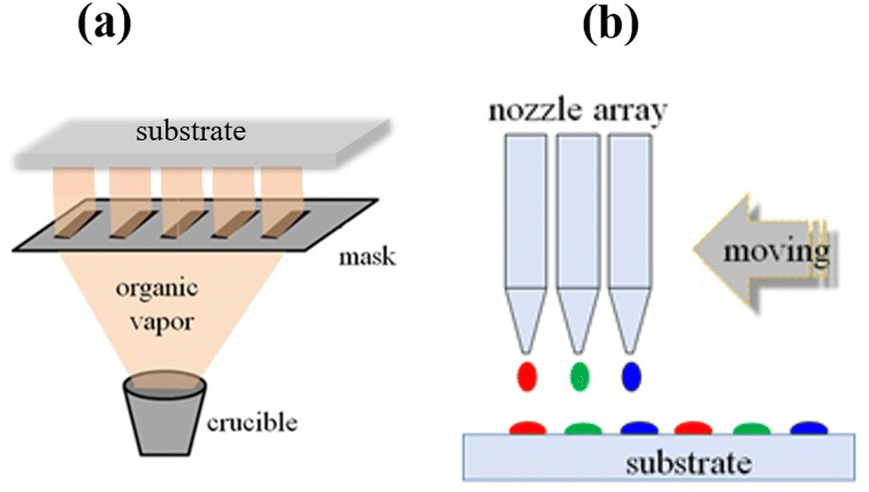 | ||
| Fig. 1 Schematic diagrams of thin-film fabrication: (a) vacuum evaporation and (b) inkjet printing. | ||
Alternatively, the solution process is capable of employing all kinds of luminescent compounds, including small molecules, dendrimers, and polymers for device fabrication. For example, spin-coating utilizes the prepared solution containing the organic material dissolved in suitable solvents to deposit uniform films on a substrate. Basically, the solution dropped on the substrate is spun at a high speed to form the film by the centrifugal force and solvent evaporation.3,4 The quality of the film depends on the solution system, the spin parameters such as spin-time, speed, atmosphere, and post treatments.5–7 Once spin-coating starts, the solution covers the entire substrate quickly and the thickness of the deposited film cannot be tuned exactly. Blade coating is usually used to prepare the films by controlling the movement of the blade. The gap between the blade and the substrate and surface tension and viscosity of the ink greatly influence the quality of the film. Alternatively, the film could also be constructed via screen printing.8 However, one of the major concerns is that the design of the inks for screen printing is constrained by strict rheological requirements during printing, mesh size/numbers, and materials solubility.
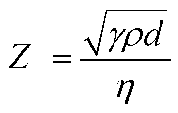
Compared with the preparation technique mentioned above, inkjet printing (see Fig. 1b) shows remarkable superiority in low-cost, mask-free, and large-area active matrix displays, due to its inherent advantages of non-contact and precise pixelation ability. Inkjet printing involves a series of computer-controlled patterned techniques and the ink droplets are directly ejected from a small nozzle onto the substrate.9 The inkjet printing technique for microscale patterning is especially attractive for full-color OLED displays. Recently, a 31-inch FHD flexible printed OLED TV via inkjet printing has been successfully demonstrated.10 There would be two different processing modes based on the different droplet behaviours during inkjet printing, namely continuous inkjet and drop-on-demand modes. The former allows the unwanted droplets to continue their paths into a catcher and then be recirculated into the nozzles. In contrast, the nozzles of the latter mode are inactive until they are demanded. To remove the influence of the drop velocity, a Z parameter, shown in eqn (1), is typically used to characterize the printability of the ink.11 The value of Z varying between 1 and 14 is demonstrated to be a reasonable one for inkjet printing.9
 | (1) |
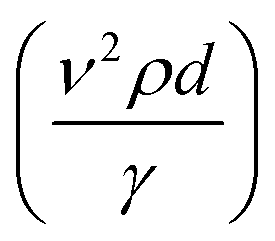
Considering the impact of the substrate, the velocity of droplets should be kept within a reasonable range. The minimum and maximum velocities of droplets are described as a Weber number formulated as eqn (2) and (3), respectively.9,12
 | (2) |
| We1/2 Re1/4 = K(r) | (3) |
 , Re is the Reynolds number
 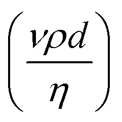 , and K(r) represents the function of the substrate roughness, respectively.
Jang et al. explored the relationship between the Z value and the drop ejection behaviour.12 Their studies suggested that small droplets (satellite drops) would be detached from the main droplets when the Z value was greater than 17.3.
Since precise droplet control and thus doped films could be directly manipulated by inkjet printing, it allowed triggering of the in situ formation of luminescent Lewis acid–base adducts (LABAs) in a well-defined area, e.g., a pixel for active matrix displays. This is totally different from the commonly used pre-mixed approach which fixes the ratios and reactions of Lewis acid and base components in the solution condition before film formation. The color tunability and the device design would be much more flexible when creating luminescent LABA via inkjet printing. Herein, we feature a comprehensive strategy and discussion based on the preparation of homogeneous color-tunable films via inkjet printing. Based on the concept of in situ post-synthesis, inkjet printing of LABAs is a particularly unique thin-film technology for display and sensing applications. Moreover, we envisage the future direction and prospects of inkjet-printing combined with the in situ post-synthesis strategy.
Host–guest configuration of inkjet printing OLEDs
The configuration of printable inks usually consists of a host matrix and a guest dopant to solve the trade-off between photoluminescence quantum yield and charge carrier transport in OLEDs. Poly-9-vinylcarbazole (PVK) is a common buffer and hole-transport material before inkjet-printing of the emitting layers (EMLs) in OLEDs, owing to its suitable energy level and excellent film quality. Alternatively, PVK possesses a high triplet energy level (2.6 eV) which could confine the excitons in the emission zone as either the host or the hole-transport layer (HTL).13 When PVK is insoluble in the selected solvent for the EML, PVK functions very well as the buffer layer which planarizes the surface roughness produced by inkjet printing. For instance, in 2021, Liu et al. fabricated red, green and blue phosphorescent OLEDs using the ink formulations with the co-host based on two small molecular compounds and the binary solvents (o-dichlorobenzene and 1-chloronaphthalene) inkjet-printed onto the PVK-based HTL.14In 2000, Yang et al. fabricated two bilayer inkjet-printed OLEDs containing PVK as the HTL and buffer layer.15 The EML was composed of tris(4-methyl-8-quinolinolato)Al (III) (Almq3) and (4-(dicyanomethylene)-2-methyl-6-(4-dimethyl aminostyryl)-4H-pyran) (DCM) as the neat emitters, respectively, which resulted in green-blue and orange-red emissions. However, due to the concentration quenching in the absence of a host, the external quantum efficiencies (EQEs) of both devices were less than 0.1%. Although PVK is widely used in the spin-coated phosphorescent OLEDs, the poor electron transport properties result in the imbalanced charge injection and transport which deteriorate the device efficiency. In 2003, Gong et al. reported electrophosphorescent devices based on the inkjet-printing and screen-printing techniques, respectively fabricated by using a blend of PVK and 2-tert-butylphenyl-5-biphenyl-1,3,4-oxadiazol (PBD) as the mixed host and a heavy-metal complex as the guest, which led to bright and efficient devices.16 Singh et al. developed an iridium-based phosphorescent dye and prepared the inks by mixing the emitter with PVK and PBD in the solvent of 1,2-dichlorobenzene.17 The device fabricated by inkjet printing realized an EQE of 2.5% and a peak luminance of over 10![[thin space (1/6-em)]](https://www.rsc.org/images/entities/char_2009.gif) 000 cd m−2.
000 cd m−2.
In 2011, Ma's group fabricated small molecular OLEDs by inkjet printing of the EML of 2-(t-butyl)-9,10-bis (20-naphthyl) anthracene (TBADN) doped with 4,40-bis [2-{4-(N,N-diphenylamino) phenyl vinyl] (DPAVBi) from the solution of chlorobenzene respectively mixed with α-chloronaphthalene and cyclohexylbenzene with high boiling points and high viscosities to create the pinhole-free EMLs.18 The current efficiency of the inkjet-printed device was only slightly lower than that of the corresponding spin-coated one (0.71 vs. 1.08 cd A−1). In 2012, Jung et al. fabricated phosphorescent OLEDs with the EQE of 11.7% by inkjet printing tris(2-phenylpyridine)iridium(III) (Ir(ppy)3) doped 4,4′-Bis(carbazol-9-yl)biphenyl (CBP) as the EML. In 2019, Kang et al. investigated the impact of the co-host mixing ratio of tris(4-carbazoyl-9-ylphenyl) amine (TCTA) and pyrido [3′,2′:4,5]furo[2,3-b] pyridine (3CzPFP) on the solubility, morphology, and device efficiency.19 After optimizing the ink formulation, a high EQE of 8.9% and a low efficiency roll-off of below 10% at 1000 cd m−2 were achieved in the inkjet-printed OLED. In 2020, Mu et al. reported an inkjet printable phosphorescent OLED which consisted of a new host material of 3-(3,6-di-t-butylcarbazol-9-yl)-3′-(2-(4-t-butylphenyl) benzoimidazol-1-yl)-[1,1′-biphenyl] and an iridium complex dopant of bis(2-methyldibenzo[f,h]quinoxaline)(acetylacetonate)–iridium(III) (Ir(MDQ)2(acac)).20 The inkjet-printed device showed the maximum current efficiency of 17.9 cd A−1 which was comparable with that of the spin-coated ones.
Although polymers are usually considered as one of the ideal materials for inkjet-printing due to the excellent morphologic characteristics and multi-layer deposition by means of orthogonal solvents, there are some drawbacks, such as an intrinsic difficulty in purification, inferior reproducibility, and clogged nozzles due to high viscosity.21 Compared with polymers, the versatile small molecular luminescent materials would be favorable in practical applications for achieving high-efficiency and stable OLEDs, since they have well-defined structures, ease of purification, controllable reproducibility, and low viscosity. However, in many cases, it is challenging to prepare uniform films using the inkjet-printing process with only small molecules, especially for the multi-layer deposition. Recrystallization, phase separation, and coffee-rings of small materials are obstacles to forming nm-scale amorphous films for high-performance OLEDs.22
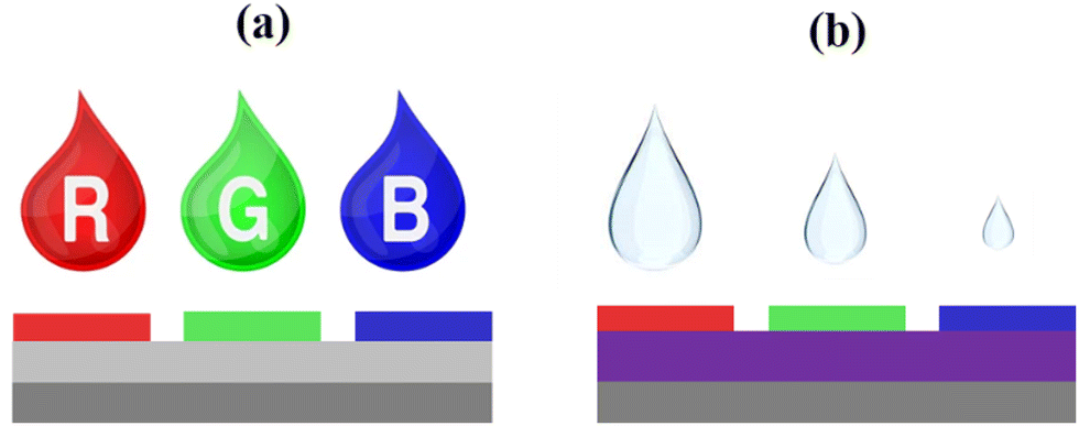
As shown in Fig. 2, the conventional inkjet printing of full-color displays employs the major solutions, i.e., red, green, and blue. Each solution most likely is composed of a host–guest system and mixed solvents. This definitely complicates the device optimization since different inkjet printing recipes are required for the individual emissive film. Apart from the complicated organic synthesis, luminescent materials could be generated by manipulating the interactions of Lewis acids with the electron-deficient properties and conjugated fluorescent compounds. In such cases, one of the options is to deposit a layer of the Lewis base as the seeding layer. The color tunability depends on the amount of the Lewis acid inkjet-printed onto the seeding layer, and vice versa. Ideally, only a single component solute, either a Lewis acid or a Lewis base, is required to prepare the ink. As illustrated in Fig. 2b, full-color displays are achievable via in situ post-synthesis via inkjet printing if the luminescent LABA is sensitive to the concentration of the ink.
 | ||
| Fig. 2 Schematic illustrations of conventional (a) and in situ post-synthesis (b) approaches to generate full-color displays via inkjet printing. | ||
As a proof-of-concept, the fluorescent molecule containing spirodifluorene and 1,3,5-triazine moieties, namely DTSF-2-DP-TRZ, and an aryl borane (BCF) were employed as the Lewis base and Lewis acid, respectively.23 A novel strategy of in situ post-synthesis based on fast Lewis acid–base interaction has been proposed by our group (see Fig. 3). Unexpectedly, the bandgap and the singlet–triplet splitting (ΔEST) were both narrowed down due to the coordination chemistry of the Lewis acid–base pair.24 This concurrently induced the thermally activated delayed fluorescence (TADF) and thus the triplet excitons underwent the reverse intersystem crossing (RISC) process, which significantly improved the utilization of triplet excitons under the electric excitation. The effect of the coordination induced TADF mechanism was also confirmed by the calculated spatial separation of the distributions of the highest occupied molecular orbital (HOMO) and the lowest unoccupied molecular orbital (LUMO), shown in the insets of Fig. 3. Experimentally, it was also identified by the prolonged delayed fluorescence lifetimes once BCF was mixed with DTSF-2-DP-TRZ. It is well-known that the small ΔEST is one of the prerequisites to open the triplet exciton up-conversion channels, which is also essential to achieve high-performance OLEDs. As expected, under the optimization of solvent system and film thickness, the EQE was greatly improved and surpassed the upper limit (5%) of the conventional fluorescent devices, which confirmed that triplet excitons are effectively utilized in the RISC process.
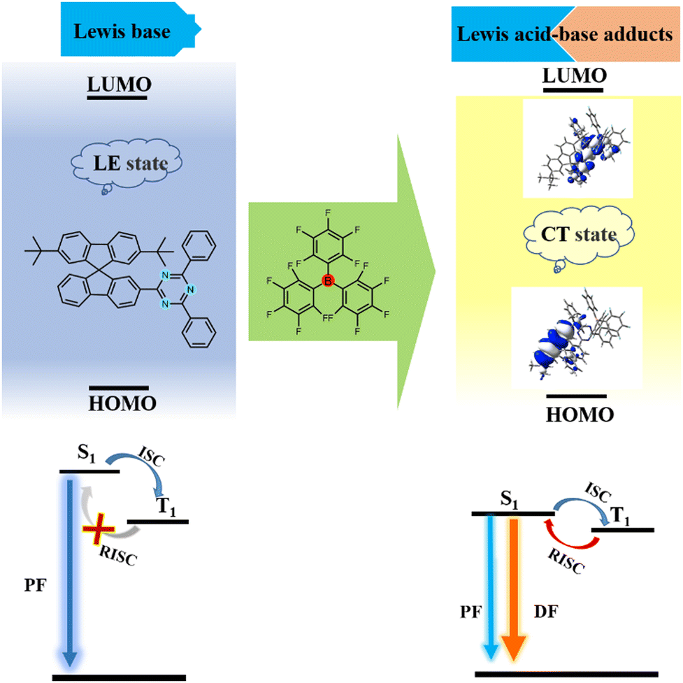 | ||
| Fig. 3 Luminescent mechanisms of the Lewis base before and after adding the Lewis acid. | ||
As the common complexing agents, Lewis acids are usually doped with the polymers to enhance the conductivity while the luminescence intensity would be quenched dramatically.25 Based on this consideration, we fabricated OLEDs by inkjet printing of the single component of BCF onto the seeding layer of DTSF-2-DP-TRZ mixed with PVK which was prevented from being dissolved in the solvent completely. Surprisingly, the ink concentration used for inkjet printing significantly affect the amount of the generated Lewis acid–base adducts and thus effectively tuned the emissive colors from deep-blue to orange-red. Alternatively, the color tunability could be demonstrated by simply repeating the times of inkjet printing. The single-component-solute ink exhibits great advantages, such as easy preparation, long storage time, low viscosity, and fast nozzle cleaning. Unlike the conventional inkjet printing of the EML shown in Fig. 2a, the concentration and luminescence quenching effects can be effectively alleviated at the interface between the inkjet-printed layer and the seeding layer which was partially dissolvable by the ink solvents to form the self-host-like emissive zones. To realize the full-color pixelations via the conventional inkjet printing, the ink cartridges containing different light-emitting materials are demanded. In contrast, the in situ post-synthesis strategy requires only one cartridge with the single solute, which would be more powerful for precisely controlling the EL wavelengths by adjusting the printing times, printing sequence, and printing dot spacing, respectively.
Thin-film morphology control of inkjet printing
Morphology optimization
To achieve successful applications for inkjet-printed OLEDs, attention should be paid to the key factors to enable the formation of uniform films, including the ink formulation, viscosity, surface energy control, substrate structures, and drying conditions.22,26 The surface energy as well as surface morphology determine the wettability of a homogeneous substrate which can be modulated by controlling of the hydrophilicity or hydrophobicity of the pixel-defined substrate.27,28 In 2011, Ding et al. adopted a binary solvent system by mixing chlorobenzene with cyclohexylbenzene which possessed a higher boiling point and higher viscosity to improve the film-forming properties of the inkjet-printed small molecular EML.18 Their study demonstrated that the higher boiling point and the higher viscosity were respectively the decisive factors of thermodynamics and kinetics to dewet the films. Nevertheless, the inkjet-printed device performance was still lower than that of the spin-coated device. In 2016, Wei et al. reported a cross-linkable electron transport material and found that cross-linkable units could improve the solubility and promote the formation of compact films.1 The device based on the inkjet-printed electron-transport material achieved the maximum EQE of 13.8%, which was comparable with that of spin-coated OLEDs (15.6%). Zhou and co-workers developed printable halogen-free binary solvents and modulated the ratio of the assistant solvent to enable the homogeneous film morphology of the EML.21 The surface properties of the substrates and the influence of the annealing temperature on the film quality had also been systematically studied. The inkjet-printed device showed the superior luminance and efficiency, compared with the spin-coated OLEDs.In 2019, Hu et al. reported two novel Ir(III) complexes with the excellent solubility and film formation ability.29 They fabricated the simple device structure with the inkjet-printed HTL and EML. The inkjet-printed device exhibited a higher EQE (7.2%) than the spin-coated one (5.3%), which was ascribed to the different surface roughness of thin-films processed via these two different techniques. Liu et al. developed the two printable Ir(III) complexed polydendrimers.30 By using the iridium precursor complexes, their comparative study suggested that the introduction of the solublizing steric hindrance groups and polymerization could effectively enhance the film-forming ability. The inkjet-printed device with greenish-blue emission based on polydendrimers achieved the maximum current efficiency of 1.81 cd A−1 and the maximum luminance of 642 cd m−2. Mu et al. developed a new host with highly soluble and amorphous properties.20 It is found that the morphology of the EML strongly depended on the substrates and the solvents. After rationally selecting the solvent and HTL, a uniform EML was obtained and the device achieved the maximum current efficiency of 17.9 cd A−1 which was comparable with that of the spin-coated device. Zheng et al. obtained a smooth EML by modifying the weight ratio of the inkjet-printed host material and emitter and fabricated the inkjet-printed blue OLEDs with a maximum EQE of 5.03% and the maximum luminance of 3743 cd m−2.31 Liu et al. adopted PVK as the HTL to improve ink spreading and film uniformity. Eventually, the fabricated red, green and blue phosphorescent OLEDs achieved the high luminance of 2812, 2366, and 2286 cd m−2, respectively.14
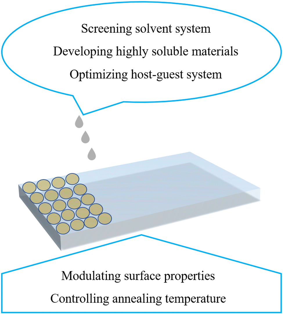
In order to acquire the good film morphology of LABAs, we optimized the process of fiml-formation by designing a suitable seeding layer, rationally tuning the solvent system of the ink, and controlling the substrate heating conditions.23 We selected PVK as an additive for the small-molecular seeding layer of the Lewis base to the reduce film roughness and slightly changed the solvent resistance. The binary solvent system, i.e., chlorobenzene and cyclohexanone, was used to regulate an appropriate Z value which guaranteed the solution to form the stable and uniform droplets. The drying conditions were also optimized by delicately controlling the substrate temperature. Finally, the uniform EML was prepared and employed to evaluate the EL and encryption properties. Based on this investigation, as shown in Fig. 4, we figure out the general rules to realize the uniform and highly emissive films for displays and sensing.
 | ||
| Fig. 4 Strategies to optimize the film morphology via inkjet printing. | ||
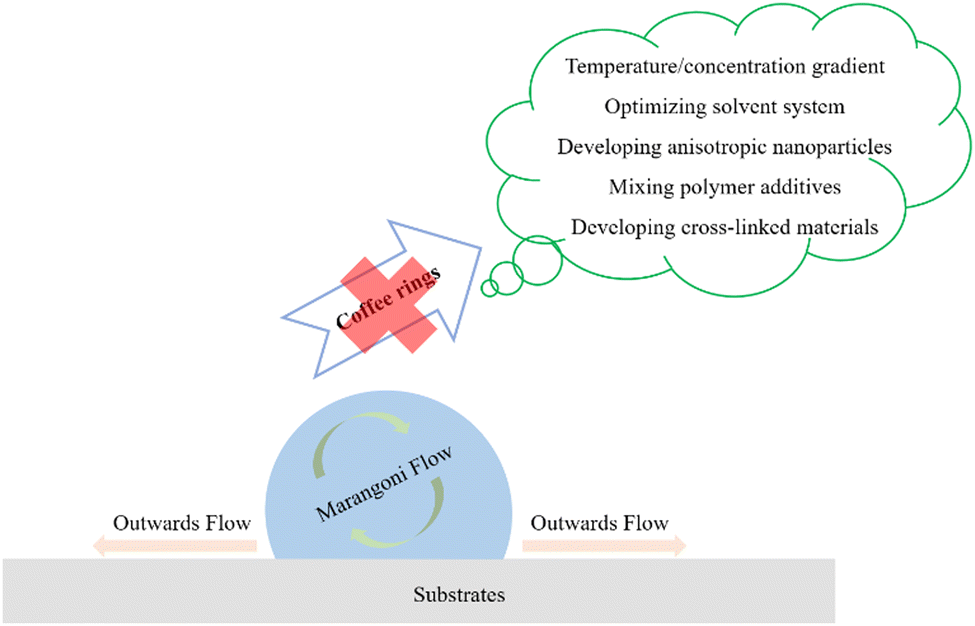
Suppression of the coffee-ring
The film morphology has a predominant impact on the overall performances of the optoelectronic devices. During inkjet printing, the solutes tend to stay or aggregate along with the periphery of the droplet covered and then dried on the substrate. This creates a dense and ring-like deposit, leading to the lower thickness inside. This is known as the coffee-ring effect, which affects the morphology and uniformity of the inkjet-printed thin-film. It is proposed that coffee rings are attributed to the capillary flow induced by the droplet evaporation at a pinned contact line.32To effectively suppress the coffee-ring effect during inkjet printing, a Marangoni flow should be induced to overcome the capillary force. The concentration gradient could modulate the Marangoni flow. Kim et al. fabricated the uniform conductive patterns through the inward Marangoni flow by adding the composite solvents with high boiling point and low surface tension.33 In 2008, Soltman et al. studied the effect of the droplet spacing and the substrate temperature on the inkjet-printed line morphology.34 A uniform film can be inkjet-printed at intermediate spacings and temperature, and a cooled substrate was favorable to suppress edge evaporation rate and thus eliminate the coffee rings.
In 2011, Yunker et al. found that anisotropic particles can be used to eliminate the coffee-ring effect because the strong long-ranged interparticle capillary effectively inhibited the outward flow.35 Jiang et al. obtained flat quantum-dot films without coffee rings by employing the mixed solvents of 1,2-dichlorobenzene with cyclohexylbenzene to reduce surface tension and introducing a poly-etherimide (PEI) modified ZnO nanoparticle layer to increase the surface free energy.36 The maximum luminance of the device based on inkjet-printed green quantum dots reached 12000 cd m−2. In 2018, Li et al. reported that dendrimers as monodisperse building blocks were capable of circumventing the coffee-ring effect to form homogeneous film via in situ gelation triggered by a thioacetate–disulfide transition which counterbalanced the capillary forces.37 Yu et al. improved the thickness uniformity by adding the assistant solvent with the high boiling point and high viscosity to the main solvent.38 The low evaporation rate and the high viscosity of the mixed solvents could effectively resist the radial flow induced by the fast evaporation, leading to the decrease of solution volume and thus coffee rings.
Liu et al. fabricated perovskite nanocomposite microarrays with the excellent morphology by using the polymer poly(vinylpyrrolidone) (PVP) as an additive which increased the viscosity and then eliminated the outward capillary flow which accounted for the coffee-ring effect.39 In 2020, Gao et al. constructed perovskite microarrays with a uniform surface and no coffee rings via inkjet printing of the perovskite quantum-dot ink, which was optimized to strengthen the Marangoni flow and balance the capillary flow by tuning the volume ratios of dodecane with a high boiling point and toluene with a low boiling point.40 In 2021, Li et al. reported that the coffee-ring effect can be successfully circumvented via optimizing the thickness of the interfacial layer PVP on the hydrophobic HTL and the temperature during the inkjet printing stage.41 The optimized inkjet-printed perovskite light-emitting diodes realized the EQE of 9% with a high brightness of 3640 cd m−2. Recently, Yoon et al. investigated the effects of the combination of different solvents on the inkjet-printed pixel pattern quality. Their study has shown that the mixed solvents with different boiling points were effective in reducing the roughness of the film surface. After optimizing the condition of the ink formulation, a uniform stripe without the remarkable coffee-ring defects was formed.42 In 2022, Han et al. constructed a supramolecular conjugated polymer with 3D cross-linked networks which impeded the transport of the aggregates to the droplet edges, and thus suppressed the coffee-ring effect and obtained a high-quality and continuous film.43
Based on the strategies discussion above, there are many successful tactics to overcome the coffee-ring effect during the inkjet printing process. Basically, controlling the capillary flow and preventing the pinning of the contact line are the key approaches. These are closely related to the physical properties of the inks used in inkjet printing. The surface energy of the substrate plays a vital role in the wetting behaviors and film formation during inkjet printing. To modulate the ink properties, one of the most effective ways is to introduce the mixed solvents, e.g., high- and low-boiling points solvents to modulate the evaporation flux along the droplet edges. Following the general rules to tackle with coffee rings indicated in Fig. 5, the uniform and highly luminescent films are achievable when the process condition and ink formulation are appropriately controlled. Most importantly, rationally modulating the solvent properties of the inks is one of the most effective and promising way to eliminate the coffee rings.
 | ||
| Fig. 5 Approaches to tackle with coffee rings. | ||
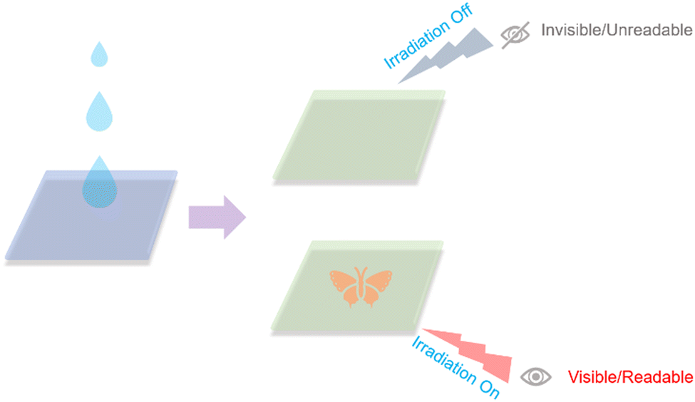
In situ process for anticounterfeiting and encryption applications
Anti-counterfeiting technologies are urgently required and have attracted considerable attention due to the great demand in information security.44 Recently, photoluminescent materials, including metal nanoclusters, nanocomposites, quantum dots, nanocrystal, hydrogels, and lanthanide complexes, have been rationally synthesized and applied for information storage and encryption applications due to their unique properties of vivid visualization, facile identification, and difficulty in duplication. In situ fabrication of light-emitting materials via inkjet printing possesses advantages of facile procedures and easy construction of large area films and arbitrary patterns.Bao et al. introduced monodispersed microspheres into the inks to in situ fabricate a dot-matrix-constructed 2D pattern with the regularly arranged pixels which revealed the applications in encoding and anticounterfeiting.45 In 2018, Feng et al. reported an optical encoding and encryption nanohybrid based on variable valence Eu2+/Eu3+ co-encapsulated where Eu3+ was partially in situ reduced to Eu2+.46 When exposed to acidic or basic vapor, the nanohybrid exhibited the time-gated response due to the different intensity and lifetimes of Eu2+ and Eu3+ ions. In 2019, Sun et al. reported in situ monitoring of gelation and self-healing processes via turn-on fluorescence -by covalent bond-induced emission of the fluorescent gels with the aggregated-induced emission properties.47 By coding these multi-color fluorescent self-healing gels, the fluorescence codes could only be read out under UV light. The emerging perovskite patterns could be used for anti-counterfeiting as well.
Shi et al. developed perovskite quantum-dot patterns by in situ inkjet printing the ink containing the perovskite precursors onto the polymer films.48 The emission of perovskite patterns can be easily turned from blue to red by varying the halides in precursor solution from Cl to Br and I, respectively. The fabricated 2D codes with the microdisk arrays weren’t visible under sunlight but easily recognized under UV excitation.
Liu et al. reported in situ inkjet-printed perovskite nanocomposite patterns with the excellent homogeneity at the macro scale.39 They fabricated two-dimensional codes and bar-codes with green emission under UV light while totally transparent in the ambient environment. In 2020, Li's group demonstrated the fingerprint arrays by introducing in situ grown perovskite crystals for multi-level anticounterfeiting.49 After spin coating a poly (methyl methacrylate) (PMMA) layer onto perovskite patterns, 3D height information from perovskite crystals can be transformed into the colorful 2D interferometric fringes.
Hydrogels with luminescent properties exhibit promising applications in information encryption. Li et al. constructed hybrid hydrogels with luminescence on–off switching behavior via in situ copolymerization of acrylamide, lanthanide complexes, and diarylethene photochromic units.50 The fabricated luminescent patterns using hydrogel blocks with various colors were masked under the irradiation of UV light (300 nm) while the encoded information turned to be readable under irradiation of visible light (>450 nm).
Liu's group reported a luminescent 2D nanocomposite and a strategy that the desired luminescence patterns can be produced by in situ printing the eggshell membrane from CuSO4 solution with dithiothreitol solution at room temperature. The luminescence patterns vanished and reappeared when treated with ethanol and NaBH4, respectively.51 In 2020, Wang et al. obtained a series of binuclear lanthanide complexes via in situ self-condensation reaction, in which the Tb-based complex exhibited the potential application in the visual detection.52 The fabricated patterns and codes using the Tb-based complex showed significant differences between white-light and UV-light conditions.
In 2022, Feng et al. developed a stable nanocrystal with a high polar solvent resistance and thermal stability via an in situ surface coordination reaction.53 Based on the different capacities of polar solvent resistance and thermal stability between zero-dimensional Cs4PbBr6 and the coordinated Cs4PbBr6–Zn(moi)2, they fabricated the optical anticounterfeiting labels by using these two nanocrystals as light-sensitive security inks. Zhou et al. prepared Au nanoassemblies with the necklace-like and spherical nanoarchitectures featuring the tunable colors of the amphiphilic block copolymer-assisted self-assembly via in situ synthesis.54 The encrypted information could be decrypted stepwise by regulating the wavelength of excitation light.
Given the simple synthesis and remarkable luminescent properties of LABAs with the conjugated components, it is feasible to promote the optical anticounterfeiting applications (see Fig. 6). We successfully fabricated the sophisticated QR code patterns and color-tunable letters via in situ post-synthesis assisted and controlled by inkjet printing.23
 | ||
| Fig. 6 Schematic diagram of generating anti-counterfeiting and encryption films via inkjet printing of LABAs. | ||
For instance, by controlling the printing times of the diluted BCF ink at a fixed concentration onto the Lewis-base film with the deep-blue fluorescence DTSF-2-DP-TRZ, the emissive colors of the encoded patterns and the letters gradually bathochromic-shifted from bluish-green to orange-red under UV light, which was ascribed to the dose of BCF dominated generation of the luminescent LABAs.23
The encrypted information could only be authenticated by the external stimuli of UV light. Furthermore, since the LABAs with different amounts of BCF exhibited different delayed lifetimes, more applications of the analogues in the time-gated encryption are envisaged and conceivable. This investigation evidenced the strategy of in situ post-synthesis combined with the inkjet printing would be very attractive and versatile.
Conclusions and perspectives
By virtue of the non-contact, precise patterning, mask-free, on-demand, and low material consumption, inkjet printing affords a facile and low-cost processing platform which has been regarded as a promising technology to achieve large-area, high-resolution array, and cost-effective mass production of optoelectronic films and devices. In this feature article, we summarized the recent advances in rationally controlling the ink formulation and thin-film process by inkjet printing for optoelectronic applications. We specify the in situ post-synthesis of the luminescent Lewis acid–base adducts via inkjet printing. Our work provides a simple and cost-effective strategy to evoke the thermally activated delayed fluorescence characteristics from a conjugated fluorescent compound, which would be universal for creating color-tunable emission, time-gated responses, and even more efficient electroluminescence. An in-depth study of the intermolecular coordination effect on the frontier molecular orbital energy levels was exemplified and explored for displays and encryption.The in situ post-synthesis provides a facile and alternative way to avoid time-consuming and tedious molecular syntheses. The simplified ink formulation and processing recipes enables the growth of the optoelectronic thin films with homogeneous morphology, fine patterns, and large area via inkjet printing technology. By combining the merits of inkjet printing technology and in situ post-synthesis, the desired compounds are expected to be generated instantaneously at the on-demand substances. The combination of in situ post-synthesis and inkjet printing is a promising strategy for a variety of optoelectronic applications, e.g., organic light-emitting diodes,55 perovskite light-emitting diodes,56 anticounterfeiting labels,57 thin film transistors,58 biomedical diagnosis,59 solar cells,60 and sensors.61 To increase the versatility of this strategy, the inkjet-printable materials, flow characteristics of droplets, morphology of the interfaces as well as coordination interactions between Lewis acid and base are worth further investigation.
Conflicts of interest
There are no conflicts to declare.Acknowledgements
The authors acknowledge the financial support from the National Natural Science Foundation of China (No. 51873159 and 62175189). G. X. acknowledged the funding support from the Program for Promoting Academic Collaboration and Senior Talent Fostering between China and Canada, Australia, New Zealand and Latin America (2021-109) and the Open Fund of Key Laboratory for Preparation and Application of Ordered Structural Materials of Guangdong Province, Shantou University (No. KLPAOSM202003).References
- C. Wei, J. Zhuang, Y. Chen, D. Zhang, W. Su and Z. Cui, Chem. Eur. J., 2016, 22, 16576–16585 CrossRef CAS PubMed.
- Q. Xue and G. Xie, Adv. Opt. Mater., 2021, 9, 2002204 CrossRef CAS.
- J. M. Chan and M. Wang, Nano Lett., 2022, 22, 5891–5897 CrossRef CAS PubMed.
- X. Zheng, R. Huang, C. Zhong, G. Xie, W. Ning, M. Huang, F. Ni and F. B. Dias, Adv. Sci., 2020, 7, 1902087 CrossRef CAS PubMed.
- X. Wang, P. She and Q. Zhang, SmartMat, 2021, 2, 299–325 CrossRef CAS.
- N. Kang, S. Cho, E. E. Leonhardt, C. Liu, S. V. Verkhoturov, W. H. H. Woodward, M. J. Eller, T. Yuan, T. C. Fitzgibbons, Y. P. Borguet, A. A. Jahnke, A. N. Sokolov, T. McIntire, C. Reinhardt, L. Fang, E. A. Schweikert, L. P. Spencer, G. Sun, G. Xie, P. Trefonas and K. L. Wooley, J. Am. Chem. Soc., 2022, 144, 8084–8095 CrossRef CAS PubMed.
- L. Zhou, F. Ni, N. Li, K. Wang, G. Xie and C. Yang, Angew. Chem., Int. Ed., 2022, 61, e202203844 CAS.
- D. A. Pardo, G. E. Jabbour and N. Peyghambarian, Adv. Mater., 2000, 12, 1249–1252 CrossRef CAS.
- H. Abdolmaleki, P. Kidmose and S. Agarwala, Adv. Mater., 2021, 33, 2006792 CrossRef CAS PubMed.
- J. G. Lee, Z. Zhao, D. Fu and X. Yan, SID Int. Symp. Dig. Tech. Pap., 2022, 53, 993–997 CrossRef.
- J. E. Fromm, IBM J. Res. Dev., 1984, 28, 322–333 Search PubMed.
- D. Jang, D. Kim and J. Moon, Langmuir, 2009, 25, 2629–2635 CrossRef CAS PubMed.
- J. G. Tait, E. Witkowska, M. Hirade, T.-H. Ke, P. E. Malinowski, S. Steudel, C. Adachi and P. Heremans, Org. Electron., 2015, 22, 40 CrossRef CAS.
- L. Liu, D. Chen, J. Xie, J. Piao, Y. Liu, W. Wang, K. Cao and S. Chen, Org. Electron., 2021, 96, 106247 CrossRef CAS.
- Y. Yang, S.-C. C, J. Bharathan and J. Liu, J. Mater. Sci.: Mater. Electron., 2000, 11, 89–96 CrossRef CAS.
- X. Gong, J. C. Ostrowski, D. Moses, G. C. Bazan and A. J. Heeger, Adv. Funct. Mater., 2003, 13, 439–444 CrossRef CAS.
- M. Singh, H. S. Chae, J. D. Froehlich, T. Kondou, S. Li, A. Mochizuki and G. E. Jabbour, Soft Matter, 2009, 5, 3002–3005 RSC.
- Z. Ding, R. Xing, Q. Fu, D. Ma and Y. Han, Org. Electron., 2011, 12, 703–709 CrossRef CAS.
- Y. J. Kang, R. Bail, C. W. Lee and B. D. Chin, ACS Appl. Mater. Interfaces, 2019, 11, 21784–21794 CrossRef CAS PubMed.
- L. Mu, M. He, C. Jiang, J. Wang, C. Mai, X. Huang, H. Zheng, J. Wang, X.-H. Zhu and J. Peng, J. Mater. Chem. C, 2020, 8, 6906–6913 RSC.
- L. Zhou, L. Yang, M. Yu, Y. Jiang, C. F. Liu, W. Y. Lai and W. Huang, ACS. Appl. Mater. Interfaces, 2017, 9, 40533–40540 CrossRef CAS PubMed.
- Z. Zhan, J. An, Y. Wei, V. T. Tran and H. Du, Nanoscale, 2017, 9, 965 RSC.
- H. Liu, Y. Tang, A. Ying, Y. Gao, X. Chen, L. Zhou, J. Lin and G. Xie, Chem. Eng. J., 2022, 444, 136642 CrossRef CAS.
- H. Liu and G. Xie, Beilstein J. Org. Chem., 2022, 18, 825–836 CrossRef CAS PubMed.
- B. Yurash, D. X. Cao, V. V. Brus, D. Leifert, M. Wang, A. Dixon, M. Seifrid, A. E. Mansour, D. Lungwitz, P. J. Santiago, K. R. Graham, N. Koch, G. C. Bazan and T.-Q. Nguyen, Nat. Mater., 2019, 18, 1327 CrossRef CAS PubMed.
- W. Chen, W. Guo, Y. Mou, Z. Du, P. Tang, W. Su and D. Zhang, Chin. J. Lumin., 2018, 39, 1451–1457 CrossRef CAS.
- J. Z. Wang, Z. H. Zheng, H. W. Li, W. T. S. Huck and H. Sirringhaus, Nat. Mater., 2004, 3, 171–176 CrossRef CAS PubMed.
- R. Cobas, S. Muñoz-Pérez, S. Cadogan, M. C. Ridgway and X. Obradors, Adv. Funct. Mater., 2015, 25, 768–775 CrossRef CAS.
- Y.-X. Hu, T. Lin, X. Xia, W.-Y. Mu, Y.-L. Sun, W.-Z. He, C.-T. Wei, D.-Y. Zhang, X. Li and Z. Cui, J. Mater. Chem. C, 2019, 7, 4178–4184 RSC.
- X. Liu, Z. Yu, M. Yu, X. Zhang, Y. Xu, P. Lv, S. Chu, C. Liu, W.-Y. Lai and W. Huang, ACS Appl. Mater. Interfaces, 2019, 11, 26174–26184 CrossRef CAS PubMed.
- X. Zheng, Y. Liu, Y. Zhu, F. Ma, C. Feng, Y. Yu, H. Hu and F. Li, Opt. Mater., 2020, 101, 109755 CrossRef CAS.
- M. Kuang, L. Wang and Y. Song, Adv. Mater., 2014, 26, 6950–6958 CrossRef CAS PubMed.
- D. Kim, S. Jeong, B. K. Park and J. Moon, Appl. Phys. Lett., 2006, 89, 264101 CrossRef.
- D. Soltman and V. Subramanian, Langmuir, 2008, 24, 2224–2231 CrossRef CAS PubMed.
- P. J. Yunker, T. Still, M. A. Lohr and A. G. Yodh, Nature, 2011, 476, 308–311 CrossRef CAS PubMed.
- C. Jiang, Z. Zhong, B. Liu, Z. He, J. Zou, L. Wang, J. Wang, J. Peng and Y. Cao, ACS Appl. Mater. Interfaces, 2016, 8, 26162–26168 CrossRef CAS PubMed.
- H. Li, D. Buesen, R. Williams, J. Henig, S. Stapf, K. Mukherjee, E. Freier, W. Lubitz, M. Winkler, T. Happe and N. Plumere, Chem. Sci., 2018, 9, 7596–7605 RSC.
- X. Yu, R. Xing, Z. Peng, Y. Lin, Z. Du, J. Ding, L. Wang and Y. Han, Chin. Chem. Lett., 2019, 30, 135–138 CrossRef CAS.
- Y. Liu, F. Li, L. Qiu, K. Yang, Q. Li, X. Zheng, H. Hu, T. Guo, C. Wu and T. W. Kim, ACS Nano, 2019, 13, 2042–2049 CAS.
- A. Gao, J. Yan, Z. Wang, P. Liu, D. Wu, X. Tang, F. Fang, S. Ding, X. Li, J. Sun, M. Cao, L. Wang, L. Li, K. Wang and X. W. Sun, Nanoscale, 2020, 12, 2569–2577 RSC.
- Y. Li, Z. Chen, D. Liang, J. Zang, Z. Song, L. Cai, Y. Zou, X. Wang, Y. Wang, P. Li, X. Gao, Z. Ma, X. Mu, A. El-Shaer, L. Xie, W. Su, T. Song and B. Sun, Adv. Opt. Mater., 2021, 9, 2100553 CrossRef CAS.
- D. G. Yoon, Y. J. Kang, R. Bail and B. D. Chin, J. Inf. Disp., 2020, 22, 91–98 CrossRef.
- Y. Han, L. Bai, X. An, M. Xu, C. Wei, Z. Lin, M. Yu, J. Lin, L. Sun, N. Sun, C. Wei, L. Xie, X. Ding, Q. Wei, C. Yin, C. Li, W. Su and W. Huang, CCS Chem., 2022, 4, 3529–3539 CrossRef CAS.
- R. Arppe and T. J. Sørensen, Nat. Rev. Chem., 2017, 1, 0031 CrossRef CAS.
- B. Bao, M. Li, Y. Li, J. Jiang, Z. Gu, X. Zhang, L. Jiang and Y. Song, Small, 2015, 11, 1649–1654 CrossRef CAS PubMed.
- P. F. Feng, M. Y. Kong, Y. W. Yang, P. R. Su, C. F. Shan, X. X. Yang, J. Cao, W. S. Liu, W. Feng and Y. Tang, ACS Appl. Mater. Interfaces, 2019, 11, 1247–1253 CrossRef CAS PubMed.
- J. Sun, J. Wang, M. Chen, X. Pu, G. Wang, L. Li, G. Chen, Y. Cai, X. Gu and B. Z. Tang, Chem. Mater., 2019, 31, 5683–5690 CrossRef CAS.
- L. Shi, L. Meng, F. Jiang, Y. Ge, F. Li, X.-G. Wu and H. Zhong, Adv. Funct. Mater., 2019, 29, 1903648 CrossRef.
- Y. Liu, Y. Zheng, Y. Zhu, F. Ma, X. Zheng, K. Yang, X. Zheng, Z. Xu, S. Ju, Y. Zheng, T. Guo, L. Qian and F. Li, ACS Appl. Mater. Interfaces, 2020, 12, 39649–39656 CrossRef CAS PubMed.
- Z. Li, H. Chen, B. Li, Y. Xie, X. Gong, X. Liu, H. Li and Y. Zhao, Adv. Sci., 2019, 6, 1901529 CrossRef CAS PubMed.
- C. Li, C. Shao, L. Li, X. Liu and M. Liu, Photochem. Photobiol. Sci., 2019, 18, 2942–2951 CrossRef CAS PubMed.
- H. F. Wang, Z. H. Zhu, J. M. Peng, B. Yin, H. L. Wang, H. H. Zou and F. P. Liang, Inorg. Chem., 2020, 59, 13774–13783 CrossRef CAS PubMed.
- X. Feng, P. Xu, J. Liu, X. Zhao, J. Cao and J. Liu, Inorg. Chem., 2022, 61, 17590–17598 CrossRef CAS PubMed.
- T. Zhou and X. Jiang, Chem. Sci., 2022, 13, 12107–12113 RSC.
- H. Jiang, J. Jin, Z. Wang, W. Wang, R. Chen, Y. Tao, Q. Xue, C. Zheng, G. Xie and W. Huang, Research, 2021, 2021, 9525802 CrossRef CAS.
- Z. Gu, Z. Huang, X. Hu, Y. Wang, L. Li, M. Li and Y. Song, ACS Appl. Mater. Interfaces, 2020, 12, 22157–22162 CrossRef CAS PubMed.
- H. Kim, J. Seo, N. Seong, T. Kim, S. Lee and Y. Hong, SID Int. Symp. Dig. Tech. Pap., 2019, 50, 1321–1324 CrossRef CAS.
- G. Mattana, A. Loi, M. Woytasik, M. Barbaro, V. Noël and B. Pirol, Adv. Mater. Technol., 2017, 2, 1700063 CrossRef.
- S. Barui, A. K. Panda, S. Naskar, R. Kuppuraj, S. Basu and B. Basu, Biomaterials, 2019, 213, 119212 CrossRef CAS PubMed.
- B. Yang, Y. Bai, R. Zeng, C. Zhao, B. Zhang, J. Wang, T. Hayat, A. Alsaedi and Z. Tan, Org. Electron., 2019, 74, 82–88 CrossRef CAS.
- M. Luo, Z. Liu, Q. Wang, R. Liu, Y. Xu, K. Wang, X. Shi and S. Ye, ACS. Appl. Mater. Interfaces, 2022, 14, 16621–16630 CrossRef CAS PubMed.
| This journal is © The Royal Society of Chemistry 2023 |