
 Open Access Article
 This Open Access Article is licensed under a
 Creative Commons Attribution 3.0 Unported Licence
Grass-like alumina nanoelectrodes for hierarchical porous silicon supercapacitors†
Kirill
Isakov
a,
Olli
Sorsa
 b,
Taina
Rauhala
b,
Santeri
Saxelin
b,
Tanja
Kallio
b,
Harri
Lipsanen
a and
Christoffer
Kauppinen
*a
b,
Taina
Rauhala
b,
Santeri
Saxelin
b,
Tanja
Kallio
b,
Harri
Lipsanen
a and
Christoffer
Kauppinen
*a
aDepartment of Electronics and Nanoengineering, Micronova, Aalto University, P.O. Box 13500, FI-00076, AALTO, Finland. E-mail: christoffer.kauppinen@gmail.com
bDepartment of Chemistry and Materials Science, Aalto University, P.O. Box 16100, FI-00076, AALTO, Finland
First published on 8th November 2022
Abstract
With the development of microscale and standalone electronic devices the demand for microscale energy storage is increasing. Micro-supercapacitors are emerging as the candidate for microscale energy storage, especially when combined with energy harvesters. In this work, we enhance the capacitance of porous silicon (PS) supercapacitor electrodes up to 4× by adding a new high-surface-area nanoelectrode on the existing topography, thus forming a hierarchical 3D supercapacitor electrode that can be used in micro-supercapacitor applications. The nanoelectrode is based on grass-like alumina (GLA) – a recently reported conformal nanoporous coating – with two surrounding TiN films, all materials deposited by atomic layer deposition. The GLA nanoelectrode can be deposited conformally on complex topographies like here on PS, as the total thickness of the electrode structure does not exceed 200 nm allowing it to be fitted in existing electrodes. The GLA nanoelectrode increased the capacitance of the PS supercapacitors alone by up to fourfold or 4× and reduced the self-discharge to a mere 25% loss after 20 h compared to a TiN coated PS reference and state-of-the-art PS both with significantly higher losses. The GLA nanoelectrode showed remarkable stability for 10![[thin space (1/6-em)]](https://www.rsc.org/images/entities/char_2009.gif) 000 galvanostatic cycles with a decrease in the capacitance only by 5% and no structural changes were identified from SEM images. Microelectronics compatible processing, the conformal deposition process and the nanoscale thickness of the GLA nanoelectrode allow it to enhance 3D electrodes commonly used in micro-supercapacitors.
000 galvanostatic cycles with a decrease in the capacitance only by 5% and no structural changes were identified from SEM images. Microelectronics compatible processing, the conformal deposition process and the nanoscale thickness of the GLA nanoelectrode allow it to enhance 3D electrodes commonly used in micro-supercapacitors.
Introduction
Advances in small or even microscale electronic devices, as well as portable and standalone electronic devices increase the demand for microscale energy storage units and power sources.1 Microscale energy and power systems are required for further advances in micro-electromechanical systems (MEMS), nanorobotics, mobile and remote sensors, communication devices, portable and wearable personal electronics, and especially in implantable medical devices along with other self-powered micro- and nanosystems.1–3Currently, self-powered microsystems primarily rely on thin film batteries as their energy storage.1 However, batteries are limited in their lifetime and power output, and microbatteries are not an exception. Supercapacitors can be quickly charged or discharged, which means fast energy transport,4–6 and are able to sustain a large number of cycles, often more than a million cycles, before degradation,1 making them a promising candidate as the required alternative for batteries.
In conventional supercapacitors, the energy is stored as a thin electrochemical double layer at the electrode–electrolyte interface (capacitive process). Alternatively, energy can be stored through reduction/oxidation of the electrode surface (faradaic process). With the faradaic processes, a much higher energy density can be reached but it occurs much more slowly and drags down the efficiency of the device which is why they cannot be utilized when considering devices with an extremely high power. Currently conventional supercapacitors are too large to be integrated with microscale electronic devices, therefore micro-supercapacitors compatible with microelectronics fabrication must be used.
These micro-supercapacitors have gained attention in recent years, and some approaches utilize various 3D architectures to allow an increased energy density1 such as interdigital deep reactive ion etched silicon beams,7 carbon microrods,8–10 interdigital micromolded activated carbon,11 porous silicon,12 porous carbon nanotubes and/or graphene.13,14 When using porous silicon (PS) as the active electrode material for the micro-supercapacitor, a thin TiN coating (5–30 nm) has been shown to improve the stability, conductivity and capacitance of the PS structure.15,16 Additionally, TiN coated PS has been shown to exhibit excellent wettability with aqueous and organic electrolytes and superior electrolyte wettability compared to just PS both with aqueous and organic electrolytes.17
Atomic layer deposition (ALD) is known for the ability to conformally coat complex 3D structures.17–22 ALD has also been widely utilized in supercapacitors, mainly for the deposition of pseudocapacitive active materials and to create a protective layer on the support material and/or to enhance the wettability.17,23,24 TiN has also been used as a pseudocapacitive material25 but we did not notice any pseudocapacity in aqueous Na2SO4. Recently, grass-like alumina (GLA) a nanostructured conformal thin film based on the ALD of Al2O3 has been reported26 and used for various applications including broad band and omnidirectional antireflection coatings for glass26 and packaged black silicon photodiodes,27 superhydrophobic antireflection coatings,28 and for enhanced IR absorbers.29
In this work we demonstrate hierarchical porous silicon supercapacitors with improved characteristics such as energy density, capacitance and self-discharge by conformally coating the porous silicon substrate with a GLA nanoelectrode. The GLA nanoelectrode is made by sandwiching the GLA nanostructure between two ALD TiN films. Microstructured PS is conformally coated with this GLA nanoelectrode to achieve a hierarchical structure with higher energy density/charge storage in a coin cell supercapacitor and is suitable for silicon-based micro-supercapacitors with various geometries, including interdigitated configuration. The GLA nanoelectrode is continuous and regular even on 40:1 aspect ratio PS. Finally, we investigate the electrochemical behavior of the assembled supercapacitor cells and establish the capacitance enhancement by adding the GLA nanoelectrode, as well as investigate the cell behavior during 10000 charge–discharge cycles.
Experimental
Hierarchical electrode fabrication
Porous silicon (PS), which composes the base structure of the supercapacitor electrodes, was purchased from SiLiMiXT. PS layers with a pore size of 5 μm ± 10% and porous layer thicknesses of 50 μm and 200 μm were prepared on 6 inch P type silicon wafers with a resistivity of 30–50 Ω cm. Wafers were pre-cut into 10 × 10 mm2 chips by the supplier. In total, 4 types of supercapacitor cells were prepared using 50 μm and 200 μm deep PS without a GLA nanoelectrode (only passivated with TiN) and with a GLA nanoelectrode (coated with TiN-GLA-TiN system), and 3 chips were dedicated to each cell (2 chips are needed to make the capacitor, and 1 extra was prepared for reserve).All PS chips were dipped into HF for 1 min to strip off the native SiO2 (Fig. 1b and c). Immediately after the oxide strip, the chips entered the ALD reactor for TiN deposition via thermal ALD (Fig. 1d). The deposition proceeded for 750 cycles at 500 °C with TiCl4 and NH3 as precursors, and N2 as a carrier gas targeting at 15 nm thickness. TiCl4 was pulsed for 100 ms with 60 sccm carrier gas flow, and NH3 was pulsed for 100 ms with 80 sccm carrier gas flow. The ALD TiN layer thicknesses were calculated from a known growth-per-cycle (GPC) GPC = 0.2 Å for this specific process, at this temperature for this tool. After this, half of the chips were used as supercapacitor plates as such (3 chips with 50 μm PS and 3 chips with 200 μm PS) as shown in Fig. 1d (referred to in the text as PS cells), and the other half was further processed with a GLA nanoelectrode (same number of chips). The next step for the ones with the GLA nanoelectrode is the deposition of Al2O3 by ALD (Fig. 1e). Thermal ALD deposition was executed for 130 cycles at 120 °C with 200 ms trimethylaluminum and 200 ms H2O pulses, N2 gas carried both precursors to the reaction chamber with a flow of 150 sccm, resulting in 11 nm (GPC = 0.85 Å) of alumina which was verified by He–Ne ellipsometry from monitor samples of flat Si. The deposited Al2O3 was transformed into GLA by immersion into de-ionized water (DIW) at 90 °C for 30 min (Fig. 1f); this process is described elsewhere in detail.26 Whole chips were immersed and then dried with a N2 gun. The final step in the GLA nanoelectrode process is the deposition of a top TiN layer (Fig. 1g). This layer was produced with the same process as the bottom TiN layer, but the target thickness was 10 nm, which corresponds to 500 ALD cycles. Al2O3 deposition was carried out in a BENEQ TFS-500 ALD system, and TiN deposition was carried out in a Picosun SUNALE R-200 Advanced ALD system. Both materials were deposited via thermal ALD processes.
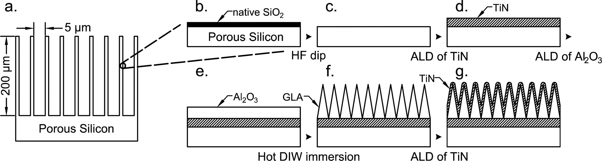 | ||
| Fig. 1 Fabrication steps (b–g) of a high surface area hierarchical electrode based on grass-like alumina. The GLA nanoelectrode is grown here on the surface of porous silicon (a), and this schematic demonstrates the 200 μm deep porous silicon used in this work. Note that the height of the GLA layer is higher than the thickness of the as-deposited Al2O3 layer. | ||
Scanning electron microscope (SEM) images of the supercapacitor chips with a GLA electrode were taken at a cross-section before and after galvanostatic cycling using Zeiss Supra 40 field emission SEM. Cross-sections were obtained by cleaving the supercapacitor chips along Si crystal planes.
Cell assembly
Symmetrical sandwich cells were assembled using CR 2032 coin cell cases (Shenzhen Gaojueneng Technology Co., Ltd), ∅ 19 mm and 260 μm thick glass fiber separators (GF/A, Whatman plc), stainless steel spacers ∅ 15.5 mm, 0.5 mm thick (MTI) and stainless steel wave springs ∅ 14.5 mm, 0.3 mm thick (MTI). 0.5 M Na2SO4 (J.T. Baker) dissolved in ultrapure ion-exchanged Milli-Q water (Merck Millipore) was used as the electrolyte. Details of the assembly are shown in Fig. 2. A PS sample was positioned in the middle of the coin cell bottom (Fig. 2a) and the separator was placed on top of it and 200 μl of the electrolyte was added (Fig. 2b). An identical sample was positioned on top of the separator for the symmetrical cell structure (Fig. 2c). A stainless steel spacer and wave spring were placed on top of the sample (Fig. 2d) and the coin cell top was used to close the cell (Fig. 2e). In order to guarantee that all the pores were filled with the electrolyte, the measurement protocol was started the day after the assembly.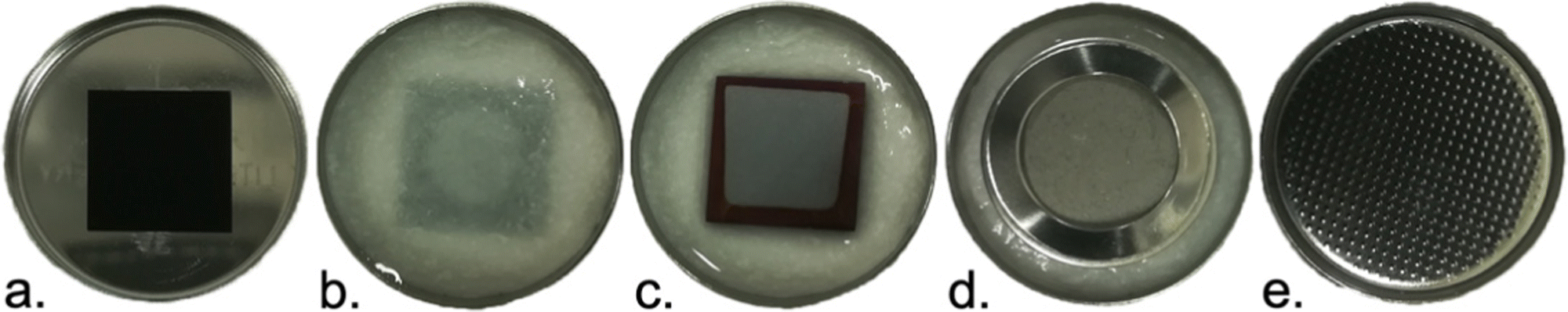 | ||
| Fig. 2 Coin cell assembly. | ||
Electrochemical characterization
The electrochemical measurements were conducted using an AUTOLAB PGSTAT302N potentiostat and Nova 2.1 software (Metrohm). All the tests were carried out at room temperature. The voltage window of the system was examined with cyclic voltammetry (CV) by performing 2 cycles at 50 mV s−1 from 0 V to an increasing upper voltage limit (0.5, 0.6, 0.7, 0.8, 0.9 and 1.0 V). The voltage window of the system is limited by the stainless-steel coin cell parts, not by the electrodes, as shown in the ESI† (Fig. S1). Based on the voltage window tests, an upper voltage limit of 0.8 V was chosen. Hence, all the electrochemical tests were performed in the cell voltage window of 0.0–0.8 V. The cell was stabilized with 50 CV cycles at 20 mV s−1 before the actual characterization. The rate capability was studied using CV and galvanostatic cycling. CV was recorded at 1, 2, 5, 10, 20, 50, 100 and 200 mV s−1 with a potential step corresponding to 0.02 s (2 cycles per scan rate, the 2nd scans were analyzed). However, due to equipment restrictions, the potential step was not smaller than 153 μV. The galvanostatic cycling was recorded at 0.002, 0.005, 0.01, 0.02, 0.05, 0.1, 0.2, 0.5 and 1 mA cm−2 (4 cycles per current, the 2nd, 3rd and 4th cycles were analyzed). The capacitance is calculated from the discharge of the galvanostatic cycling at a voltage window of 0.6–0.2 V. Electrochemical impedance spectra (EIS) were recorded from 100 kHz to 10 mHz at an open circuit voltage in zero charge with a 5 mV amplitude. The self-discharge rate of the cell was measured by charging the cell at 0.1 mA cm−2 until 80% of the full charge (0.64 V) and holding it at that voltage for 30 min before turning the cell off and recording the voltage drop for 20 h. As a durability experiment, 10000 galvanostatic cycles were recorded at a current that was equivalent to 10 s per cycle. The rate capability measurements and the EIS were remeasured after the cycling.
Results & analysis
Fig. 3 shows cross-sectional SEM images of the fabricated supercapacitor electrodes before (a and b) and after (c and d) cycling. Subfigures (a) and (c) demonstrate the microstructure of PS used as the substrate, while (b) shows the GLA nanoelectrode on the cleaved PS sidewall and (d) shows the nanostructure of the GLA nanoelectrode on the bottom of a PS pore. Fig. 3a and c correspond to the schematic in Fig. 1a and the nanostructure schematic of the electrode in Fig. 1g is shown in reality in Fig. 3b and d. In Fig. 3 the subfigure (c) contains fibers resting on the top of the PS, which originate from the separator used in the assembled supercapacitor. It can be seen from the subfigure (d) that the GLA electrode has been conformally deposited even at the bottom of the 200 μm deep PS. Comparison of images (b) and (d) concludes that there is no cycling induced degradation of the GLA electrode observable by SEM. The GLA nanoelectrode thickness does not exceed 200 nm, which allows it to fit into the structure of PS. Additional SEM images are provided in Fig. S2 (ESI†).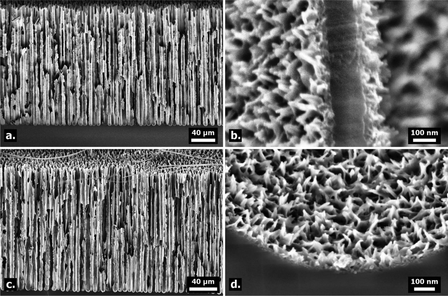 | ||
| Fig. 3 Scanning electron microscope images of the GLA nanoelectrode deposited on 200 μm deep porous silicon. (a and b) Before galvanostatic cycling; (c and d) after 10000 galvanostatic cycles. (b) The GLA nanoelectrode on the cleaved PS sidewall and (d) an image from the bottom of the PS. | ||
Fig. 4 shows the two fundamental electrochemical characterization methods for the 200 μm PS + GLA cell: cyclic voltammetry and galvanostatic cycling. In the CV curves, a rectangular shape is obtained and in the galvanostatic cycling, a triangular shape. These are the ideal shapes of an electrochemical double layer supercapacitor with the corresponding electrochemical methods which means that the cell operates with capacitive processes. With the slowest charge/discharge rates, the shapes show some non-ideal behavior due to the faradaic reaction caused by the cell components (see Fig. S1, ESI†). This is seen mainly at high cell voltages as increased faradaic current in the CV curves and as a decreasing slope in the galvanostatic charge/discharge curves. At higher rates, the faradaic reactions do not have enough time to occur to a significant degree, resulting in a mostly capacitive response of the system. Moreover, at higher rates, the self-discharge (discussed further in the end of this section) can be taken as negligible, which also affects the shape of the curves. Overall, the system works rather ideally when the rate is high enough (≥5 mV s−1 or ≥0.01 mA cm−2). Fig. S5–S20 in the ESI† contain the same data as in Fig. 4 for all the samples that were fabricated in this work.
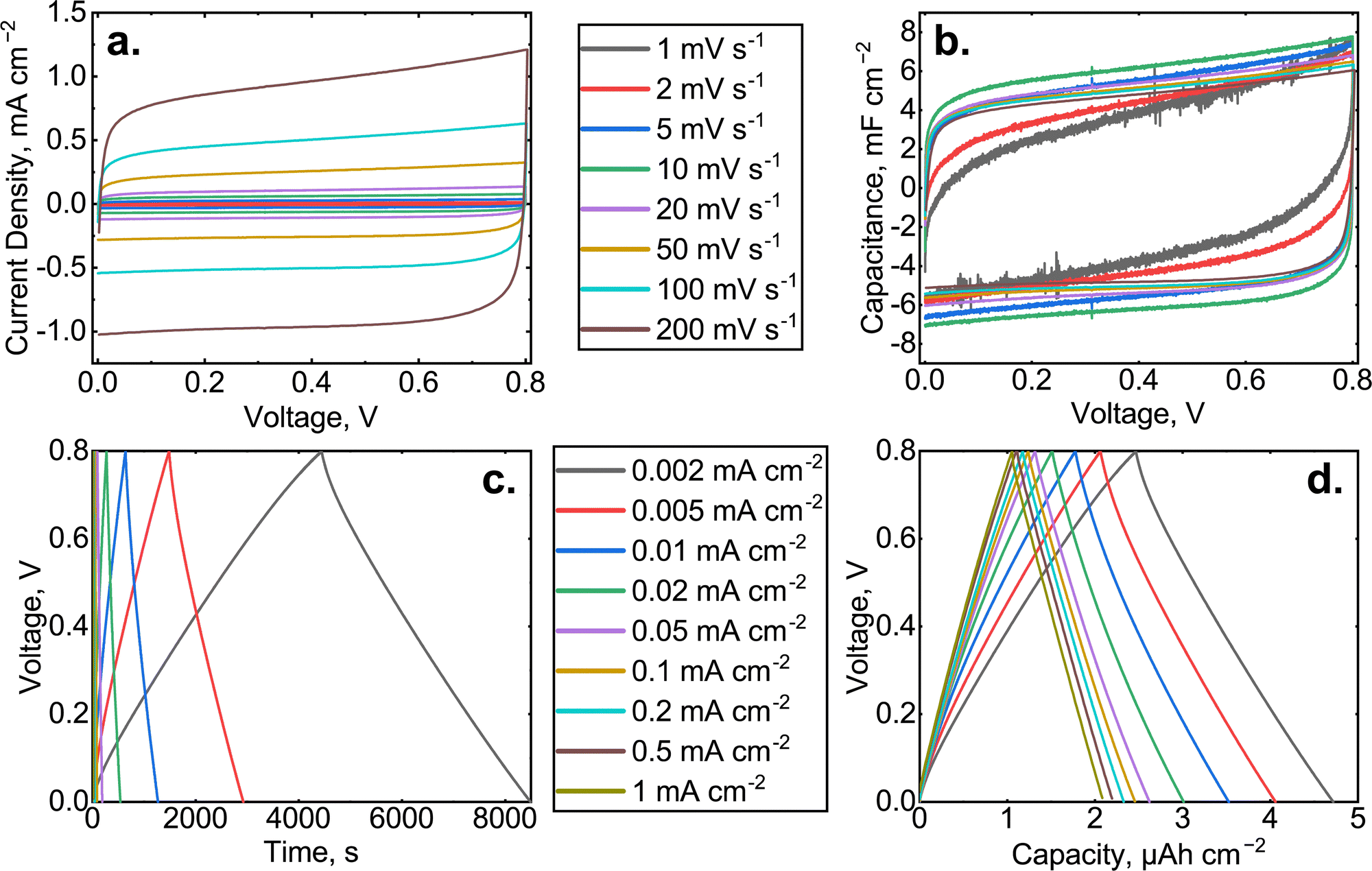 | ||
| Fig. 4 Cyclic voltammograms (a and b) and galvanostatic cycles (c and d) of the 200 μm PS + GLA cell with different charge/discharge rates. In (b), the current density has been normalized with the scan rate in order to plot the capacitance and in (d), the time has been normalized with the applied current density in order to plot the capacity. These normalizations have been carried out for a more convenient comparison between different rates. | ||
The capacitance of each cell in the galvanostatic cycling is shown in Fig. 5. The capacitance has been quantified with the same charge/discharge currents as shown in Fig. 4 and plotted before and after 10000 galvanostatic cycles. The capacitance is normalized with the area of the electrode (1 cm2) in Fig. 5a and with the total volume of the active layers in the cell in Fig. 5b. To determine the volume, the height of the PS pillars is considered as the depth of the sample. For example, the total active volume of the 200 μm PS cell is 2 × 10 mm × 10 mm × 0.2 mm = 40 mm3. The volume normalized capacitances of the 50 μm PS and 200 μm PS are almost identical. Similarly, the values for 50 μm PS + GLA and 200 μm PS + GLA are close to each other. This shows that the GLA has been conformally synthesized inside the pores between the PS pillars and it increases the area of the electrochemical double layer. The capacitance increase of the GLA nanoelectrode is 2.5–4.0-fold which is impressive. The best performing cell, 200 μm PS + GLA shows capacitance values of 5–11 mF cm−2 which is the largest areal capacitance ever reported for silicon based aqueous microsupercapacitors corresponding to 120–270 mF cm−3, depending on the applied current density.
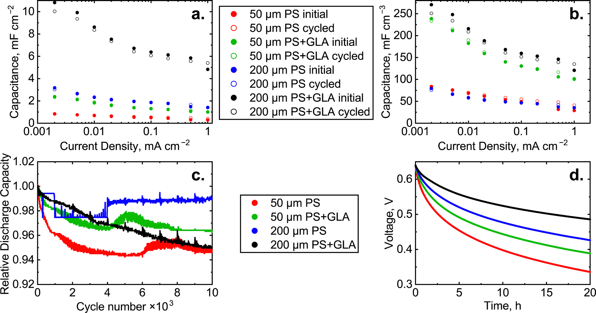 | ||
| Fig. 5 The discharge capacitances of the supercapacitor cells in galvanostatic cycling with different charge/discharge currents (a and b), the discharge capacity of the supercapacitor cells for 10000 galvanostatic cycles (c) and the self-discharge of the cell for 20 h (d). In (a), the capacitance has been normalized with the area and in (b), it has been normalized with the volume. The cycling capacities are presented relative to the average capacity of the first ten discharge cycles. For the self-discharge, the cell was charged to 0.64 V before opening the circuit. | ||
The increase of the PS cell capacitance with the addition of the GLA nanoelectrode can solely be attributed to the increase in surface area. This can be seen from the capacitance formula 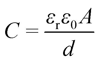 where for electrochemical double-layer capacitors εr is the relative permittivity of the electrolyte, ε0 is the vacuum permittivity, d is the effective thickness of the double-layer and A is the area of the capacitor. As the PS cell has 15 nm of TiN facing the electrolyte and the PS + GLA cell has 10 nm of TiN facing the electrolyte, the surface chemistry of these situations is the same. Therefore from the capacitance formula it can be concluded that the increase in capacitance is solely due to the increased surface area.
All the cells show a decrease of capacitance with increasing current density. With higher current, the electrochemical double layer is forced to form faster which in some cases results in a lower capacitance. In our case, the main cause of capacitance decrease is the limited diffusion rate of the electrolyte in and out of the PS pores. The capacitance decrease is higher for the samples with the GLA which is explained by the smaller volume for the electrolyte to diffuse between the pillar structure and the higher capacity which requires more electrolyte to be diffused. The 10000 galvanostatic cycles do not cause a substantial decrease in the capacitances which means that the structure of the material is stable in these conditions. The volumetric capacity of the PS cells in these measurements was ∼11 μA h cm−3 and for PS + GLA it was ∼32 μA h cm−3 at 0.1 mA cm−2. The coulombic efficiency, which is determined as the ratio of discharge and charge capacity, was >97% for all the cells when the current density was at least 0.01 mA cm−2. The volumetric energy of the PS cells in these measurements was ∼4 μW h cm−3 and for PS + GLA it was ∼12 μW h cm−3 at 0.1 mA cm−2. The energy efficiency of the cells was mainly 75–85%.
The stability of the materials was studied with galvanostatic cycling. Because the cells had major differences in capacity, the cells were cycled with a current equivalent to 10 s per cycle. This corresponds to 28 h of cycling and the current density varied in the range of 0.05–1 mA cm−2. The voltage window of the cycling was 0.0–0.8 V. The capacity decrease during galvanostatic cycling is presented in Fig. 5c. The system suffers from only minor capacity reduction as all the cells have roughly 95% or more of the initial capacity left after 10000 cycles. Generally, an increased surface area leads to a higher amount of side reactions with the electrolyte, leading to a lowered cycle life. In contrast, in the case of the GLA nanoelectrode, the cycle life is not lowered by the additional surface area provided by the GLA layer, demonstrating the excellent performance of the GLA nanoelectrode in improving the capacitance of the supercapacitor. The roughly 95% of the initial capacity left after 10000 cycles shows the viability of the GLA nanoelectrode as an approach to increase the performance of real-world supercapacitors.
One of the drawbacks of supercapacitors is their relatively high self-discharge rate.30 This means that supercapacitors cannot be used for long term energy storage because the energy efficiency decreases as the device experiences self-discharge. We tested the self-discharge rate of the studied cells by charging the device up to 80% of the maximum voltage (0.64 V) and applying that voltage for 0.5 h in order to stabilize the system and to eliminate the effects of overpotential arising during the galvanostatic charging. Then the circuit was opened, and the voltage was monitored for 20 h (Fig. 5d). The cell voltage of the best performing material, 200 μm PS + GLA, drops from 0.64 V to 0.48 V in 20 h corresponding to a 25% loss. In comparison, in the state-of-the-art devices by Grigoras et al.17 the voltage dropped from 1.2 V to 0.4 V in 20 h, a 67% loss for their device. The low self-discharge achieved by our GLA nanoelectrode devices is thus clearly favorable compared to state-of-the-art microsupercapacitors. The voltage drop (in this work) is clearly dependent on the total capacity of the cell since the cells with the highest capacity (200 μm PS) experience less voltage discharge than the 50 μm PS cells. Most remarkably, the GLA further decreases the rate of self-discharge. In terms of the self-discharge, it would be beneficial to use longer pillars, so that the charge could not escape that fast.
The electrochemical impedance spectra of the cells are presented in Fig. 6. The ideal spectrum of a double layer supercapacitor is a straight vertical line at Z′ equaling the ohmic resistance of the cell. All the spectra show a small semicircular feature at high frequencies and then rise up in an almost right angle relative to the Z′-axis. The ohmic resistance of the cell can be considered as the intercept with the Z′-axis and the area-specific ohmic resistance is similar for both PS cells (∼5 Ω cm2) and for both PS + GLA cells (∼3 Ω cm2). This means that the GLA nanoelectrode coating increases the conductivity of the material. This is probably due to the thicker TiN (roughly 15 nm below and 10 nm above the GLA) which improves the in-plane conductivity. The PS electrode has only 15 nm TiN on the side facing the electrolyte. PS pores coated with conductive layers have previously resulted in higher pore surface conductivity which results in a higher utilizable capacitance.31 For the spacer cell (see the discussion in the ESI†) the area-specific ohmic resistance in 0.5 M Na2SO4 was 1.2 Ω cm2 (Fig. S3, ESI†) which means that the silicon substrate causes a significant resistance in the system. However, for a more optimized system, the thickness of the substrate can be lower which causes less resistance. In addition, wafers with much lower resistivities for example 0.005 Ω cm are commercially available compared to the values of 30–50 Ω cm used in this work. These optimization steps would even in a conservative estimate bring down the silicon resistance by a factor of a thousand. Moreover, if the materials are used in a chip supercapacitor, the system can be designed so that there is no need for the current to travel through the whole thickness of the silicon chip.
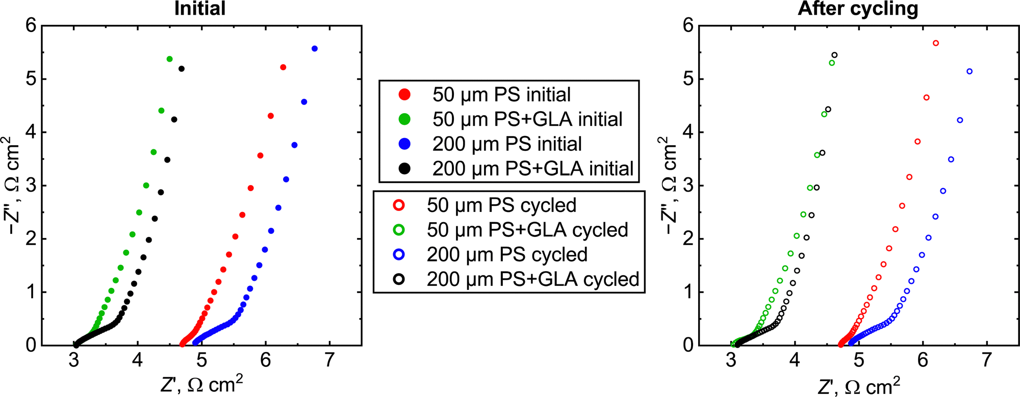 | ||
| Fig. 6 Electrochemical impedance spectra of the supercapacitor cells before (left) and after the galvanostatic cycling (right) at zero charge open circuit voltage. | ||
The width of the high frequency feature is clearly higher for the 200 μm PS than for the 50 μm one. This suggests that the feature is caused by diffusion as for the longer pillars the electrolyte has to diffuse a longer distance. The effective area-specific resistance increase of the diffusion is ∼0.2 Ω cm2 for the 50 μm and ∼0.6 Ω cm2 for the 200 μm one. Based on this, the total performance of the cell is not that highly dependent on the diffusion and even longer PS pillars could be used with this geometry. The 10000 galvanostatic cycles do not have an effect on the EIS either, demonstrating the stability of the material in the studied conditions and indicating real-world robustness of the GLA nanoelectrode.
Discussion
The fabrication techniques used for the GLA nanoelectrode are known to be scalable and accessible in batch processing, which makes it attractive for industrial applications. We have demonstrated compatibility with Si technology, which opens the route for further development of in-chip micro-supercapacitors. On the other hand, the majority of macro supercapacitors utilize various powders, and powders can also be coated by ALD methods. Additional studies are required to develop a similar method to enhance powder-based supercapacitors by GLA nanoelectrodes. Moreover, the same methodology of GLA nanoelectrode enhancement should be applicable to all-solid-state supercapacitors, ceramic and film capacitors, as well as some battery structures. Such investigations are outside the scope of this work, but they demand attention in the near future. It should be noted that the GLA synthesis can be applied to other micro-supercapacitor geometries than the sandwich structure (as done in this work), such as the interdigital structure.11TiN-GLA-TiN likely contains transitionary film at the interface of different materials, such as AlOxNy and TiOxNy. This is not particularly problematic, as the TiN and Al2O3 interface is utilized in some MOSFET structures,32 where TiN plays the role of the gate material, and Al2O3 is the gate oxide. The diffusion of oxygen from alumina into TiN is reported to be about 1 nm33 or even indetectable.34 The top TiN layer in the electrode structure presented in this work has a thickness of about 10 nm, which ensures that the electrolyte-facing surface of the electrode comprises only TiN, and the oxygen diffusion phenomena inside the electrode do not alter the system from the perspective of its application in supercapacitors. Another important characteristic for the electrode is its conductivity; it was demonstrated that the addition of GLA and TiN layers on top of TiN coated porous silicon actually improves the conductivity in the supercapacitors (see the impendence spectra presented in Fig. 6).
Table 1 shows a list of silicon based aqueous microsupercapacitor electrodes/devices with their relevant properties. The capacitance of the 200 μm PS cell (∼2 mF cm−2) is already comparable to other PS electrodes reported in the literature. With different silicon structure geometries, capacitances of 1–5 mF cm−2 have been reported.15–17,35,36,38 However, the GLA nanoelectrode boosts the capacitance of the PS electrodes to the next level (5–11 mF cm−2 or 2.5–4× increase), and no aqueous silicon microsupercapacitor reported as high a capacitance. Higher capacitance values (10–300 mF cm−2) can be achieved with porous carbon structures, such as carbon nanotubes, graphene and etched activated carbon and even higher ones (100–2000 mF cm−2) with pseudocapacitive materials utilizing faradaic processes such as oxides (e.g. RuO2, MnO2) or conductive polymers (e.g. polyaniline, polypyrrole).39 However, the pseudocapacitive materials lack in durability and rate capability resulting in lower maximum power and energy efficiency,40,41 and porous carbon electrodes often require additives such as binders or conductive additives which decrease the energy density.30 Unlike carbon-based supercapacitors, their silicon-based counterparts can be scaled down to accommodate microscale devices. Using a silicon substrate also allows production of supercapacitors on the same chips in parallel with other electronics.
| Electrode material | Electrode capacitance (mF cm−2) | Electrode thickness (μm) | Electrolyte | Voltage window (V) | Device energy (μW h cm−2) | Device power (mW cm−2) | Ref. |
|---|---|---|---|---|---|---|---|
| PS + GLA | 5–11 | 200 | 0.5 M Na2SO4 | 0.8 | 0.48 | 0.34 at 1 mA cm−2 | This work |
| PS | 1.7–3 | 200 | 0.5 M Na2SO4 | 0.8 | 0.16 | 0.34 at 1 mA cm−2 | This work |
| TiN in a PS matrix | 3.1 | 6 | 1 M NaCl | 1.2 | 0.6 | 48 | 17 |
| SiC coated Si nanowires | 1.7 | 32 | 1 M KCl | 1.0 | 0.24 | — | 35 |
| In2O3 coated PS | 1.36 | 0.8 | 1 M Na2SO4 | 1.2 | 0.21 | 0.12 | 36 |
| Graphitized C on poly-SiC | 0.743 | 0.5 | 1 M H2SO4 | 0.7 | 0.026 | 1.50 | 37 |
The PS electrodes are often very stable when coated with TiN and capacitance deterioration of 5–20% has been reported over thousands of cycles.15,17 Therefore, with the 5% capacitance decrease over 10000 cycles reported here, the stability of 200 μm PS + GLA is at least at the expected level. Since the energy of a supercapacitor device is more dependent on the voltage window than on the capacitance of the electrode materials, the aqueous system used in this work with the 0.8 V upper limit does not yield a high energy density (0.48 μW h cm−2, 12 μW h cm−3 for the 200 μm PS + GLA). Although, in comparison to the highest energy density aqueous systems on silicon these are reasonable results as a specific energy of up to 0.6 μW h cm−2 has been reported17,35–37 (see Table 1). The power densities obtained in both 200 μm cells, PS and PS + GLA, are equal to 0.34 mW cm−2 at a current density of 1 mA cm−2. This value is notably lower than for some other reported aqueous systems, even though the corresponding capacitances of those system were lower (see Table 1).
We chose aqueous 0.5 M Na2SO4 as the electrolyte because it is common in fundamental supercapacitor experiments. We have also tested organic electrolyte (1 M TEABF4 in propylene carbonate), but the cell did not provide the expected double layer capacitor-like behavior (Fig. S4, ESI†). This experiment was performed without the GLA which means that the issue relates to either the microstructure of the PS or the TiN layer, not the addition of GLA. It should be noted that with organic electrolyte the system is expected to have a lower capacitance and rate capability because of the larger ion size and slower diffusion. Due to the operation mode of ALD, the synthesis can be performed on a variety of different substrate geometries. The geometry was not optimized in this study. Therefore, a different geometry could enable the use of organic electrolyte and optimization of the substrate could result in even higher capacitance. Furthermore, other conductive materials instead of the TiN could be used, e.g. metals deposited by ALD. Nevertheless, the experiments performed in the aqueous electrolyte already show that the addition of GLA increases the capacitance of the porous silicon by a remarkable 2.5–4.0 times and is therefore highly beneficial.
Conclusions
This work demonstrates a new kind of conformal nanoelectrode for hierarchical supercapacitors made by ALD. The GLA nanoelectrode increases the capacitance of PS supercapacitors up to fourfold or 4× and consists of a TiN-GLA-TiN stack. We have shown that the GLA nanoelectrode is applicable on the complex 3D structure of porous silicon with a 40:1 aspect ratio and due to conformality of the ALD process it is suitable for large scale batch processing. The GLA enhances the surface area of the underlaying PS substrate making it applicable as a microsupercapacitor electrode especially as it uses silicon microelectronics compatible processing. The supercapacitor device with a 200 μm thick PS and 0.5 M Na2SO4 as the electrolyte achieves a specific capacitance of 5–11 mF cm−2 which is more than the best PS microsupercapacitors reported in the literature (see Table 1) but with dramatically reduced self-discharge. Although alumina is not an electrically conductive material, with the GLA nanoelectrode (TiN-GLA-TiN stack), the resistance of the PS electrode was actually decreased. The GLA nanoelectrode structure is stable over 10000 galvanostatic cycles and shows a very low self-discharge rate making it a promising surface area enhancer for PS electrode-based supercapacitors and microsupercapacitors. Furthermore, the GLA electrode enhancement can be applied to other types of (super-)capacitors both in the macro- and microscale.
Abbreviations
| PS | Porous silicon |
| ALD | Atomic layer deposition |
| GLA | Grass-like alumina |
| SEM | Scanning electrode microscope |
| CV | Cyclic voltammetry |
| EIS | Electrochemical impedance spectra |
Author contributions
The manuscript was written through contributions from all authors. All authors have given approval to the final version of the manuscript.Conflicts of interest
The authors declare the following competing financial interest: a patent application has been filed.Acknowledgements
The authors thank the Academy of Finland (project: PREIN Flagship 320187) and Business Finland (project: NANOGRA 6615/31/2019) for financial support. The authors appreciate Micronova Nanofabrication Center for continued technical support.References
- M. Beidaghi and Y. Gogotsi, Capacitive Energy Storage in Micro-Scale Devices: Recent Advances in Design and Fabrication of Micro-Supercapacitors, Energy Environ. Sci., 2014, 7(3), 867, 10.1039/c3ee43526a.
- Z. L. Wang, Toward Self-Powered Sensor Networks, Nano Today, 2010, 5(6), 512–514, DOI:10.1016/j.nantod.2010.09.001.
- Z. L. Wang and W. Wu, Nanotechnology-Enabled Energy Harvesting for Self-Powered Micro-/Nanosystems, Angew. Chem., Int. Ed., 2012, 51(47), 11700–11721, DOI:10.1002/anie.201201656.
- P. Simon and Y. Gogotsi, Materials for Electrochemical Capacitors, Materials for Sustainable Energy, Co-Published with Macmillan Publishers Ltd., UK, 2010, pp. 138–147 DOI:10.1142/9789814317665_0021.
- P. Simon and Y. Gogotsi, Capacitive Energy Storage in Nanostructured Carbon–Electrolyte Systems, Acc. Chem. Res., 2013, 46(5), 1094–1103, DOI:10.1021/ar200306b.
- L. L. Zhang and X. S. Zhao, Carbon-Based Materials as Supercapacitor Electrodes, Chem. Soc. Rev., 2009, 38(9), 2520, 10.1039/b813846j.
- W. Sun, R. Zheng and X. Chen, Symmetric Redox Supercapacitor Based on Micro-Fabrication with Three-Dimensional Polypyrrole Electrodes, J. Power Sources, 2010, 195(20), 7120–7125, DOI:10.1016/j.jpowsour.2010.05.012.
- M. Beidaghi and C. Wang, Micro-Supercapacitors Based on Three Dimensional Interdigital Polypyrrole/C-MEMS Electrodes, Electrochim. Acta, 2011, 56(25), 9508–9514, DOI:10.1016/j.electacta.2011.08.054.
- M. Beidaghi, W. Chen and C. Wang, Electrochemically Activated Carbon Micro-Electrode Arrays for Electrochemical Micro-Capacitors, J. Power Sources, 2011, 196(4), 2403–2409, DOI:10.1016/j.jpowsour.2010.09.050.
- W. Chen, M. Beidaghi, V. Penmatsa, K. Bechtold, L. Kumari, W. Z. Li and C. Wang, Integration of Carbon Nanotubes to C-MEMS for On-Chip Supercapacitors, IEEE Trans. Nanotechnol., 2010, 9(6), 734–740, DOI:10.1109/TNANO.2010.2049500.
- C. Shen, X. Wang, W. Zhang and F. Kang, A High-Performance Three-Dimensional Micro Supercapacitor Based on Self-Supporting Composite Materials, J. Power Sources, 2011, 196(23), 10465–10471, DOI:10.1016/j.jpowsour.2011.08.007.
- K. Grigoras, J. Keskinen, L. Grönberg, J. Ahopelto and M. Prunnila, Invited) Porous Silicon for Energy Storage at Microscale: Supercapacitors, ECS Trans., 2016, 75(1), 97–104, DOI:10.1149/07501.0097ecst.
- S. Nardecchia, D. Carriazo, M. L. Ferrer, M. C. Gutiérrez and F. del Monte, Three Dimensional Macroporous Architectures and Aerogels Built of Carbon Nanotubes and/or Graphene: Synthesis and Applications, Chem. Soc. Rev., 2013, 42(2), 794–830, 10.1039/C2CS35353A.
- Z.-S. Wu, X. Feng and H.-M. Cheng, Recent Advances in Graphene-Based Planar Micro-Supercapacitors for on-Chip Energy Storage, Natl. Sci. Rev., 2014, 1(2), 277–292, DOI:10.1093/nsr/nwt003.
- P. Lu, P. Ohlckers, L. Müller, S. Leopold, M. Hoffmann, K. Grigoras, J. Ahopelto, M. Prunnila and X. Chen, Nano Fabricated Silicon Nanorod Array with Titanium Nitride Coating for On-Chip Supercapacitors, Electrochem. Commun., 2016, 70, 51–55, DOI:10.1016/j.elecom.2016.07.002.
- D. S. Gardner, C. W. Holzwarth, Y. Liu, S. B. Clendenning, W. Jin, B.-K. Moon, C. Pint, Z. Chen, E. C. Hannah, C. Chen, C. Wang, E. Mäkilä, R. Chen, T. Aldridge and J. L. Gustafson, Integrated On-Chip Energy Storage Using Passivated Nanoporous-Silicon Electrochemical Capacitors, Nano Energy, 2016, 25, 68–79, DOI:10.1016/j.nanoen.2016.04.016.
- K. Grigoras, J. Keskinen, L. Grönberg, E. Yli-Rantala, S. Laakso, H. Välimäki, P. Kauranen, J. Ahopelto and M. Prunnila, Conformal Titanium Nitride in a Porous Silicon Matrix: A Nanomaterial for in-Chip Supercapacitors, Nano Energy, 2016, 26, 340–345, DOI:10.1016/j.nanoen.2016.04.029.
- C. Detavernier, J. Dendooven, S. Pulinthanathu Sree, K. F. Ludwig and J. A. Martens, Tailoring Nanoporous Materials by Atomic Layer Deposition, Chem. Soc. Rev., 2011, 40(11), 5242, 10.1039/c1cs15091j.
- M. Knez, K. Nielsch and L. Niinistö, Synthesis and Surface Engineering of Complex Nanostructures by Atomic Layer Deposition, Adv. Mater., 2007, 19(21), 3425–3438, DOI:10.1002/adma.200700079.
- D. Losic, G. Triani, P. J. Evans, A. Atanacio, J. G. Mitchell and N. H. Voelcker, Controlled Pore Structure Modification of Diatoms by Atomic Layer Deposition of TiO2, J. Mater. Chem., 2006, 16(41), 4029, 10.1039/b610188g.
- H. C. M. Knoops, M. E. Donders, M. C. M. van de Sanden, P. H. L. Notten and W. M. M. Kessels, Atomic Layer Deposition for Nanostructured Li-Ion Batteries, J. Vac. Sci. Technol., A, 2012, 30(1), 010801, DOI:10.1116/1.3660699.
- J. Ahn, C. Ahn, S. Jeon and J. Park, Atomic Layer Deposition of Inorganic Thin Films on 3D Polymer Nanonetworks, Appl. Sci., 2019, 9(10), 1990, DOI:10.3390/app9101990.
- Z. Li, J. Su and X. Wang, Atomic Layer Deposition in the Development of Supercapacitor and Lithium-Ion Battery Devices, Carbon, 2021, 179, 299–326 CrossRef CAS.
- M. Gnerlich, E. Pomerantseva, K. Gregorczyk, D. Ketchum, G. Rubloff and R. Ghodssi, Solid Flexible Electrochemical Supercapacitor Using Tobacco Mosaic Virus Nanostructures and ALD Ruthenium Oxide, J. Micromech. Microeng., 2013, 23(11), 114014 CrossRef.
- E. Kao, C. Yang, R. Warren, A. Kozinda and L. Lin, ALD Titanium Nitride on Vertically Aligned Carbon Nanotube Forests for Electrochemical Supercapacitors, Sens. Actuators, A, 2016, 240, 160–166 CrossRef CAS.
- C. Kauppinen, K. Isakov and M. Sopanen, Grass-like Alumina with Low Refractive Index for Scalable, Broadband, Omnidirectional Antireflection Coatings on Glass Using Atomic Layer Deposition, ACS Appl. Mater. Interfaces, 2017, 9(17), 15038–15043, DOI:10.1021/acsami.7b01733.
- C. Kauppinen, T. P. Pasanen, K. Isakov, M. Serué, J. Heinonen, V. Vähänissi, H. Lipsanen and H. Savin, Grass-like Alumina Coated Window Harnesses the Full Omnidirectional Potential of Black Silicon Photodiodes, Appl. Opt., 2021, 60(33), 10415–10420 CrossRef CAS PubMed.
- K. Isakov, C. Kauppinen, S. Franssila and H. Lipsanen, Superhydrophobic Antireflection Coating on Glass Using Grass-like Alumina and Fluoropolymer, ACS Appl. Mater. Interfaces, 2020, 12(44), 49957–49962 CrossRef CAS PubMed.
- K. Isakov, A. P. Perros, A. Shah and H. Lipsanen, Wide-Band ‘Black Silicon’ with Atomic Layer Deposited NbN, Nanotechnology, 2018, 29(33), 335303, DOI:10.1088/1361-6528/aac738.
- M. Lu, Supercapacitors: Materials, Systems, and Applications, John Wiley & Sons, 2013 Search PubMed.
- S. Desplobain, G. Gautier, J. Semai, L. Ventura and M. Roy, Investigations on Porous Silicon as Electrode Material in Electrochemical Capacitors, Phys. Status Solidi C, 2007, 4(6), 2180–2184, DOI:10.1002/pssc.200674418.
- D. Wu, A.-C. Lindgren, S. Persson, G. Sjoblom, M. von Haartman, J. Seger, P.-E. Hellstrom, J. Olsson, H.-O. Blom, S.-L. Zhang, M. Ostling, E. Vainonen-Ahlgren, W.-M. Li, E. Tois and M. Tuominen, A Novel Strained Si/Sub 0.7/Ge/Sub 0.3/Surface-Channel PMOSFET with an ALD TiN/Al/Sub 2/O/Sub 3//HfAlO/Sub x//Al/Sub 2/O3 Gate Stack, IEEE Electron Device Lett., 2003, 24(3), 171–173, DOI:10.1109/LED.2003.809524.
- E. O. Filatova, S. S. Sakhonenkov, A. S. Konashuk, S. A. Kasatikov and V. V. Afanas’ev, Inhibition of Oxygen Scavenging by TiN at the TiN/SiO2 Interface by Atomic-Layer-Deposited Al2O3 Protective Interlayer, J. Phys. Chem. C, 2019, 123(36), 22335–22344, DOI:10.1021/acs.jpcc.9b05800.
- I. S. Jeon, J. Park, D. Eom, C. S. Hwang, H. J. Kim, C. J. Park, H. Y. Cho, J.-H. Lee, N.-I. Lee and H.-K. Kang, Post-Annealing Effects on Fixed Charge and Slow/Fast Interface States of TiN/Al2O3/p-Si Metal–Oxide–Semiconductor Capacitor, Jpn. J. Appl. Phys., 2003, 42(3), 1222–1226, DOI:10.1143/JJAP.42.1222.
- J. P. Alper, M. Vincent, C. Carraro and R. Maboudian, Silicon Carbide Coated Silicon Nanowires as Robust Electrode Material for Aqueous Micro-Supercapacitor, Appl. Phys. Lett., 2012, 100(16), 163901, DOI:10.1063/1.4704187.
- B. Zhu, X. Wu, W.-J. Liu, H.-L. Lu, D. W. Zhang, Z. Fan and S.-J. Ding, High-Performance On-Chip Supercapacitors Based on Mesoporous Silicon Coated with Ultrathin Atomic Layer-Deposited In2O3 Films, ACS Appl. Mater. Interfaces, 2019, 11(1), 747–752, DOI:10.1021/acsami.8b17093.
- F. Liu, A. Gutes, I. Laboriante, C. Carraro and R. Maboudian, Graphitization of N-Type Polycrystalline Silicon Carbide for on-Chip Supercapacitor Application, Appl. Phys. Lett., 2011, 99(11), 112104, DOI:10.1063/1.3638468.
- D. Aradilla, F. Gao, G. Lewes-Malandrakis, W. Müller-Sebert, D. Gaboriau, P. Gentile, B. Iliev, T. Schubert, S. Sadki, G. Bidan and C. E. Nebel, A Step Forward into Hierarchically Nanostructured Materials for High Performance Micro-Supercapacitors: Diamond-Coated SiNW Electrodes in Protic Ionic Liquid Electrolyte, Electrochem. Commun., 2016, 63, 34–38, DOI:10.1016/j.elecom.2015.12.008.
- N. A. Kyeremateng, T. Brousse and D. Pech, Microsupercapacitors as Miniaturized Energy-Storage Components for on-Chip Electronics, Nat. Nanotechnol., 2017, 12(1), 7–15, DOI:10.1038/nnano.2016.196.
- J. Libich, J. Máca, J. Vondrák, O. Čech and M. Sedlaříková, Supercapacitors: Properties and Applications, J. Energy Storage, 2018, 17, 224–227 CrossRef.
- T. Rauhala, F. Davodi, J. Sainio, O. Sorsa and T. Kallio, On the Stability of Polyaniline/Carbon Nanotube Composites as Binder-Free Positive Electrodes for Electrochemical Energy Storage, Electrochim. Acta, 2020, 336, 135735 CrossRef CAS.
Footnote |
| † Electronic supplementary information (ESI) available. See DOI: https://doi.org/10.1039/d2ya00177b |
| This journal is © The Royal Society of Chemistry 2022 |